1
Standard ICs
Dual operational amplifier
BA4558 / BA4558F / BA4558N
The BA4558, BA4558F, and BA4558N are monolithic ICs with two operational amplifiers featuring low power con-
sumption and internal phase compensation mounted on a single silicon chip. These products offer high speed, a
wide band width, and low noise.
Outstanding thermal characteristics and voltage gain band width make these ICs ideal for use in a wide variety of
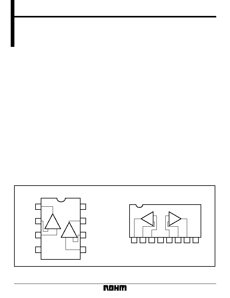
electronic circuits. The BA4558 comes in an 8-pin DIP package and is compatible with the 4558 operational amplifi-
er. The BA4558F comes in an 8-pin SOP package, and the BA4558N in an 8-pin SIP package.
ñ
Applications
Active filters
Audio amplifiers
VCOs
Other electronic circuits
ñ
Block diagram
1ch
2ch
V
CC
OUT2
Ù IN2
+ IN2
OUT1
Ù IN1
+ IN1
V
EE
4
3
2
1
8
7
5
6
+
Ù
Ù
1ch
2ch
OUT1
1
Ù IN1
2
+ IN1
3
V
EE
4
+ IN2
5
Ù IN2
6
OUT2
7
V
CC
8
+
Ù
+
Ù
BA4558 / BA4558F
BA4558N
+
ñ
Features
1) Low power dissipation of approximately 50mW
(typ.).
2) Built-in output short-circuit protection circuit.
3) Internal phase compensation.
4) No latch-up.
5) Wide range of common mode and differential volt-
age.
6) High gain and low noise.
2
Standard ICs
BA4558 / BA4558F / BA4558N
ñ
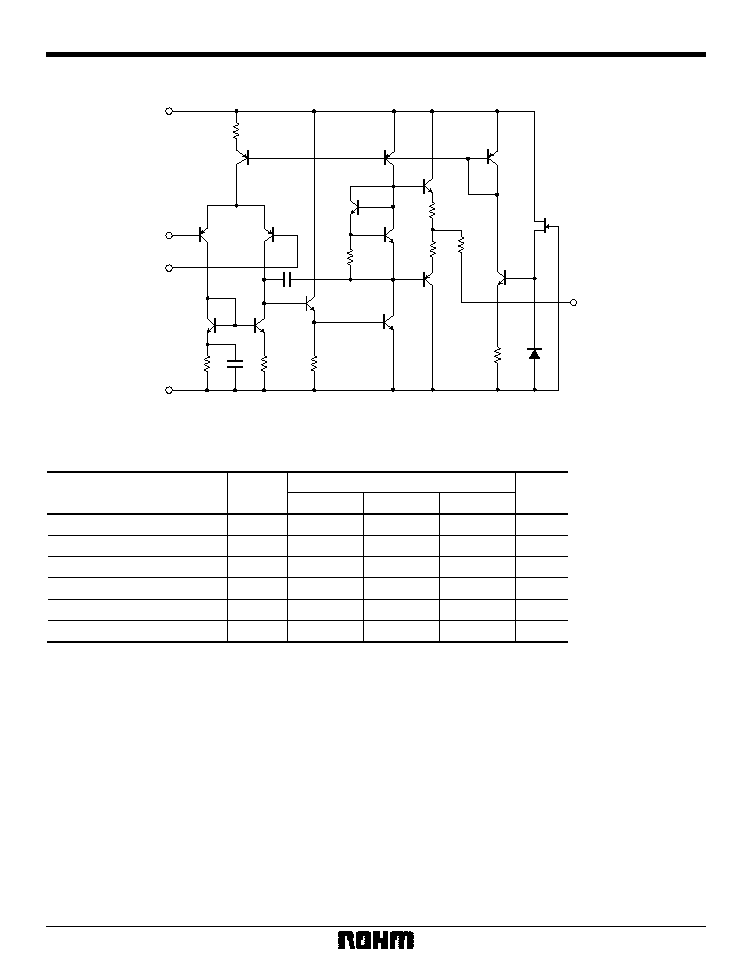
Internal circuit configuration
V
CC
Ù IN
+ IN
V
EE
R
1
R
9
R
8
R
7
R
6
R
5
R
4
R
3
R
2
Q
5
Q
13
Q
15
Q
11
Q
12
Q
14
Q
8
Q
9
Q
10
Q
6
Q
4
Q
3
Q
2
Q
1
Q
7
OUT
D
ñ
Absolute maximum ratings (Ta = 25¯C)
Parameter
Symbol
Limits
Unit
BA4558
BA4558F
BA4558N
Power supply voltage
V
CC
Ý
18
Ý
18
Ý
18
V
Power dissipation
800
550
900
mW
Differential input voltage
V
ID
Ý
30
Ý
30
Ý
30
V
Common-mode input voltage
V
I
Ý
15
Ý
15
Ý
15
V
Operating temperature
Topr
Ù 40 ~ + 85
Ù 40 ~ + 85
Ù 40 ~ + 85
¯
C
Storage temperature
Ù 55 ~ + 125 Ù 55 ~ + 125 Ù 55 ~ + 125
¯
C
Pd
Tstg
Refer to Pd characteristics diagram.
The values for the BA4558F are those when it is mounted on a glass epoxy board ( 50mm
æ
50mm
æ
1.6mm) .
3
Standard ICs
BA4558 / BA4558F / BA4558N
ñ
Electrical characteristics (unless otherwise noted, Ta = 25¯C, V
CC
= + 15V, V
EE
= Ù 15V)
Parameter
Symbol
Typ.
Max.
Unit
Input offset voltage
V
IO
--
0.5
6.0
mV
R
S
10k
Input offset current
I
IO
--
5
200
nA
Input bias current
I
B
--
60
500
nA
High-amplitude voltage gain
A
V
86
100
--
dB
Common-mode input voltage
V
ICM
Ý
12
Ý
14
--
V
Maximum output voltage
V
OH
Ý
12
Ý
14
--
V
R
L
10k
Minimum output voltage
V
OL
Ý
10
Ý
13
--
V
R
L
2k
Common-mode rejection ratio
CMRR
70
90
--
dB
R
S
10k
Power supply voltage rejection ratio
PSRR
--
30
150
ç
V / V
R
S
10k
Slew rate
S.R.
--
1.0
--
V /
ç
s
Channel separation
CS
--
105
--
dB
f = 1kHz
Conditions
Min.
R
L
2k
, V
O
=
Ý
10V
A
V
= 1, R
L
2k
ñ
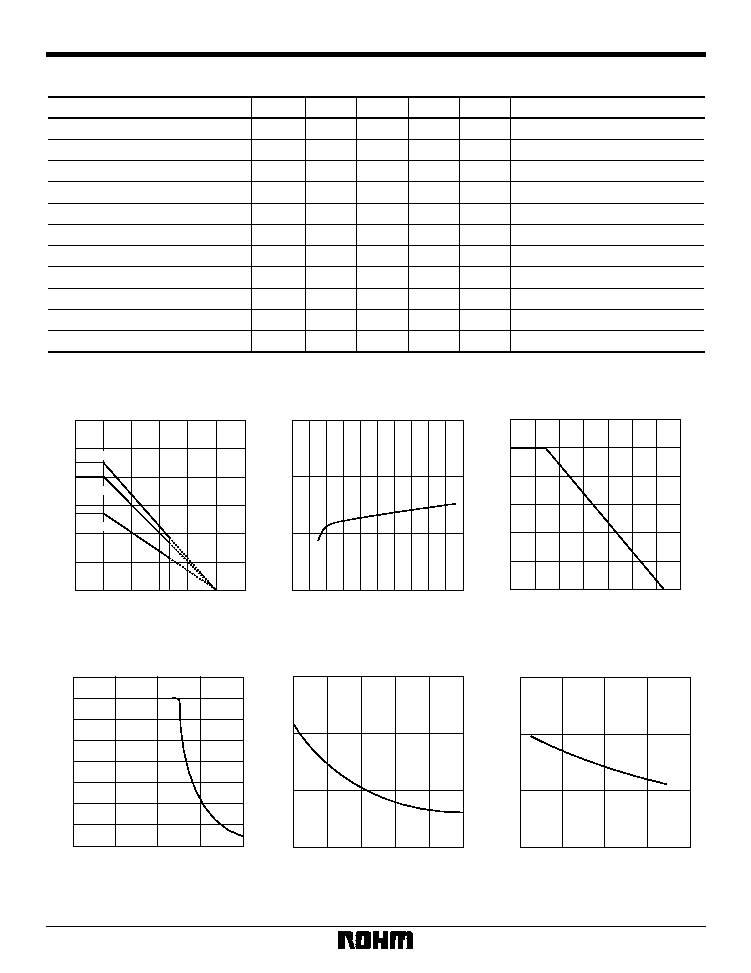
Electrical characteristic curves
Fig.1 Power dissipation vs. ambient
temperature
AMBIENT TEMPERATURE: Ta (
¯
C)
POWER DISSIPATION: Pd (mW)
1200
1000
800
600
400
200
0
0
25
50
75 85 100
125
150
BA4558N
BA4558F
BA4558
4
5
3
2
0
Ý
10
Ý
20
POWER SUPPLY VOLTAGE: V
Ý
(V)
QUIESCENT CURRENT: I
Q (
mA)
Fig.2 Quiescent current vs. power
supply voltage
1M
10M
120
100
80
60
40
20
0
1
10
100
1k
10k
100k
FREQUENCY: f (Hz)
OPEN LOOP GAIN: A
V (
dB)
Fig.3 Open loop voltage gain vs.
frequency
32
28
24
20
16
12
8
4
0
100
1k
10k
100k
1M
FREQUENCY: f (Hz)
MAXIMUM OUTPUT VOLTAGE: V
OM
(V)
Fig.4 Maximum output voltage vs.
frequency
100
80
60
40
Ù 20
0
20
40
60
80
AMBIENT TEMPERATURE: Ta (
¯
C)
INPUT BIAS CURRENT: I
B
(mA)
Fig.5 Input bias current vs. ambient
temperature
100
75
50
25
0
10
20
30
40
POWER SUPPLY VOLTAGE: V
+
(V)
INPUT BIAS CURRENT: I
B
(nA)
Fig.6 Input bias current vs. power
supply voltage
4
Standard ICs
BA4558 / BA4558F / BA4558N
+ 5
0
Ù 5
Ù 5
0
5
0
20
40
60
80
TIME (
ç
s)
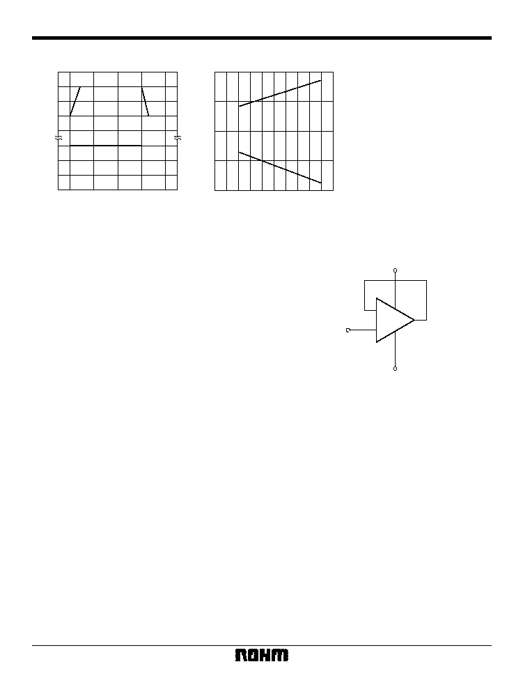
INPUT VOLTAGE OUTPUT VOLTAGE
V
IN
(V) V
OUT
(V)
Fig.7 Output response characteristics
20
10
0
Ù 10
Ù 20
0
Ý
10
Ý
20
COMMON MODE INPUT VOLTAGE: V
ICM
(V)
POWER SUPPLY VOLTAGE: V
Ý
(V)
Fig.8 Common mode input voltage vs.
power supply voltage
ñ
Operation notes
(1) Unused circuit connections
If there are any circuits which are not being used, we
recommend making connections as shown in Figure 9,
with the non-inverted input pin connected to the poten-
tial within the in-phase input voltage range (V
ICM
).
V
CC
V
EE
To potential
in V
ICM
+
Ù
Fig.9 Unused circuit connections
5
Standard ICs
BA4558 / BA4558F / BA4558N
ñ
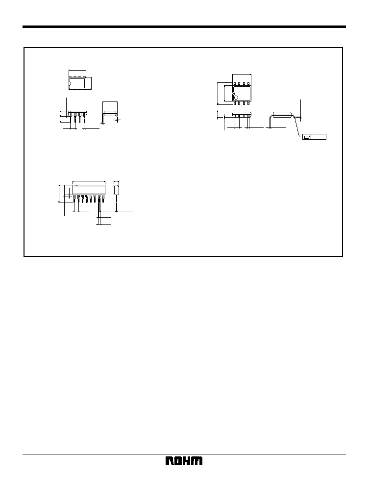
External dimensions (Units: mm)
BA4558
BA4558F
BA4558N
DIP8
SOP8
SIP8
0.5
Ý
0.1
3.2
Ý
0.2
3.4
Ý
0.3
8
5
1
4
9.3
Ý
0.3
6.5
Ý
0.3
0.3
Ý
0.1
0.51Min.
2.54
0
¯
~ 15
¯
7.62
0.4
Ý
0.1
1.27
0.15
0.3Min.
0.15
Ý
0.1
0.11
6.2
Ý
0.3
4.4
Ý
0.2
5.0
Ý
0.2
8
5
4
1
1.5
Ý
0.1
10.5
Ý
0.5
1
8
2.54
3.5
Ý
0.5
1.3
0.8
0.6
0.3
Ý
0.1
2.8
Ý
0.2
19.3
Ý
0.2
1.2
5.8
Ý
0.2