Preliminary
RT9267
DS9267-02 September, 2002
www.richtek.com
1
High Efficiency, Low Quiescent, Triple output DC-DC Converter
General Descriptions
The RT9267 is a triple output DC-DC converter IC
including two adaptive PWM controllers, one low
dropout regulator, and one voltage detector. RT9267
is capable of delivering hundreds of mA output
current and consumes only 40
Á
A quiescent current
for the whole IC.
The adaptive PWM controllers are configured for
boost applications with built-in 2A NMOS for each
channel. The proprietary adaptive PWM loop
provides PWM operation for heavier output loading
conditions and PFM for lighter loading, with seamless
auto-transition. The 500kHz switching rate reduces
the size of external passive components.
The low dropout linear regulator (LDO) is designed
with a built-in 300mA PMOS, providing 1mV/mA low
dropout voltage with respect to variant output current
values.
The voltage detector provides the supervisory
function with open collector pull-low output. All the 4
function units are adjustable, and each can be set
with two resistors in divider connection. The
reference voltage for each channel is set to 1.25V for
the two adaptive PWM controllers, and 0.86V for the
LDO and the voltage detector.
The RT9267 is in TSSOP 16 pin package which fits
space-limited hand held devices well.
Ordering Information
RT9267
Features
Two Channels of Adaptive PWM Controllers
One Channel of Low Dropout Regulator
One Voltage Detector
Low Start-Up Voltage 1.0V
Low Quiescent Current 40
Á
A for the Whole IC
High Switching Rate 550KHz
Built-In 2A Switching NMOS
Two Separated Chip Enable Control Pins
2
%
Accuracy for All Channels
Minimized External Components
Small TSSOP-16 Package
Applications
PDA
Portable Instrument
Wireless Equipment
DSC
LCD Back Bias Circuit
RF-Tags
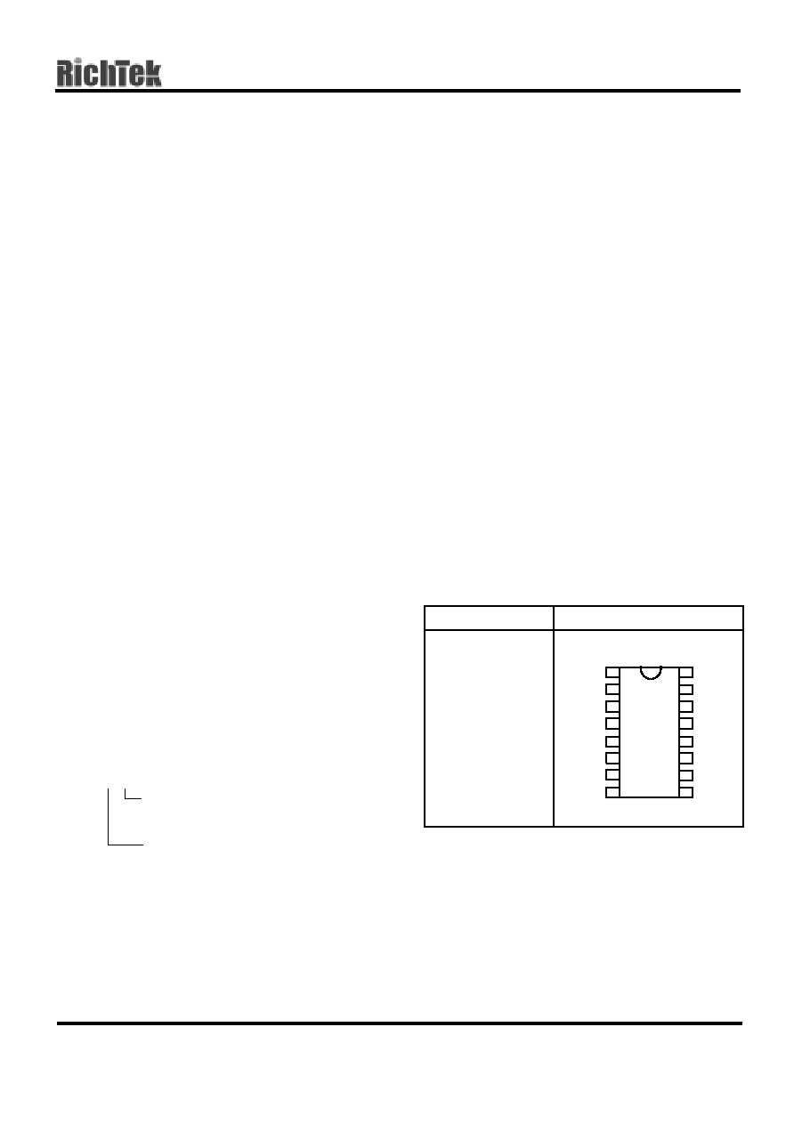
Pin Configurations
Part Number
Pin Configurations
RT9267CC
(Plastic TSSOP-16)
TOP VIEW
Operating temperature range
C: Commercial standard
Package type
C : TSSOP-16
1
2
3
4
5
6
7
8
9
10
14
13
12
11
LX1
CE1
GND
CE2
NC
LX2
NC
VDD
FB1
LFB
NC
LDOO
FB2
LBI
15
16
GND
LBO
RT9267
Preliminary
www.richtek.com
DS9267-02 September, 2002
2
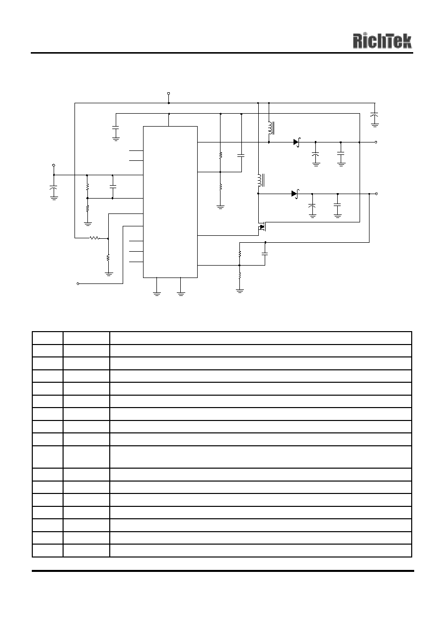
Typical Application Circuit
Pin Description
Pin No.
Pin Name
Pin Function
1
LX1
The switching pin for 1
st
PWM converter
2
CE1
Enable pin for 1
st
PWM converter and LDO. High = enable, Low = shutdown
3
GND
Ground (Both Pin3 and Pin8 should be connected)
4
CE2
Enable pin for 2
nd
PWM converter and voltage detector. High = enable, Low = shutdown
5
NC
Not connected
6
LX2
The switching pin for 2
nd
PWM converter
7
NC
Not connected
8
GND
Ground (Both Pin3 and Pin8 should be connected)
9
LBO
NMOS open drain output of the voltage detector. This pin will internally pulled low when
the voltage at LBI pin below 0.86V.
10
LBI
Input pin for voltage detector. The trip point is 0.86V.
11
FB2
Feedback input pin for 2
nd
PWM converter. Internal V
REF
for the error amplifier is 1.25V.
12
LDOO
Voltage output pin for the LDO.
13
NC
Not connected
14
LFB
Feedback pin for the LDO. Internal V
REF
for the error amplifier is 0.86V
15
FB1
Feedback input pin for 1
st
PWM converter. Internal V
REF
for the error amplifier is 1.25V
16
VDD
Input positive power pin of RT9267, and also the voltage input pin for LDO.
L1
4.7
Á
H
R5
+
+
FB2
LX2
FB1
LX1
VDD
CE1
CE2
LDOO
LFB
LBO
NC
NC
NC
GND
3
9
14
7
10
12
15
16
13
11
6
5
4
1
2
C7
1
Á
F
Q1
NMOS
C6
100
Á
F
C4
10
Á
F
R8
112K
R7
1.5M
RT9267
LBI
GND
8
L2
10
Á
H
R4
980K
R1
1.6M
+
C10
1
Á
F
C9
100
Á
F
R3
680K
R2
1.3M
C1
1
Á
F
R6
Low Battery
Warning Output
(open Collector)
Chip Enable
Chip Enable
D1
1N5819
+
C2
100
Á
F
C3
100pF
C8
0.1
Á
F
D2
1N5819
18V
3.3V
2.5V
V
IN
(1.1V ~ 3.3V)
C5
100pF
Preliminary
RT9267
DS9267-02 September, 2002
www.richtek.com
3
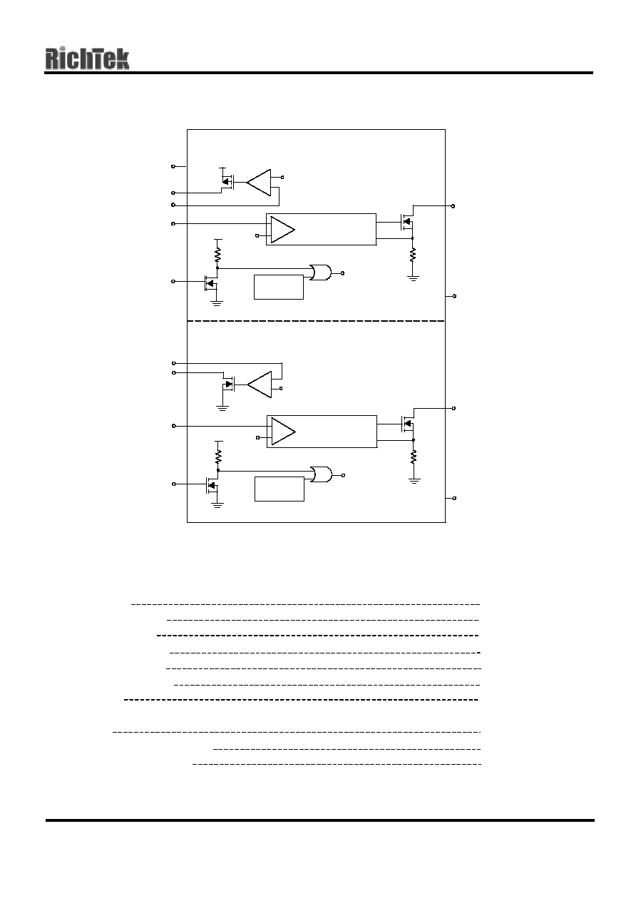
Function Block Diagram
Absolute Maximum Ratings
Supply Voltage
-0.3V to 7V
LX Pin Switch Voltage
-0.3V to (VDD + 0.8V)
LDO Output Voltage
-0.3V to (VDD + 0.3V)
Other I/O Pin Voltages
-0.3V to (VDD + 0.3V)
LX Pin Switch Current
2.5A
EXT Pin Driver Current
30mA
LBO Current
30mA
Power Dissipation, P
D
@ T
A
= 25
░
C
TSSOP-16
600mW
Operating Junction Temperature
150
░
C
Storage Temperature Range
-65
░
C ~ +150
░
C
LDOO
Loop Control Circuit
Over Temp.
Detector
LX1
GND
Shut Down
0.86V
1.25V
1
st
PWM and LDO controlled with CE1
VDD
LFB
FB1
CE1
VDD
R2
Q3
NMOS
VDD
Q2
PMOS
R1
Q1
NMOS
+
_
+
_
LBI
Loop Control Circuit
Over Temp.
Detector
LX2
GND
Shut Down
0.86V
1.25V
LBO
FB2
CE2
VDD
R2
Q3
NMOS
Q2
NMOS
R1
Q1
NMOS
+
_
+
_
1
st
PWM converter
2
nd
PWM and Voltage Detector controlled with CE2
2
nd
PWM converter

RT9267
Preliminary
www.richtek.com
DS9267-02 September, 2002
4
Electrical Characteristics
(V
IN
= 5V, C
IN
= C
OUT
= 1
Á
F, T
A
= 25
░
C, unless otherwise specified)
Parameter
Symbol
Test Conditions
Min
Typ
Max
Units
Section for Adaptive PWM Converters
Start-Up Voltage
V
ST
I
L
= 1mA
--
0.98
1.05
V
Operating VDD Range
V
DD
Start-up to I
DD
>
250
Á
A
0.8
--
6.5
*
V
Feedback Reference Voltage
V
REF
Close Loop, VDD = 3.3V
1.225
1.25
1.275
V
Switching Rate
F
S
VDD = 3.3V
--
550
--
kHz
Maximum Duty
D
MAX
VDD = 3.3V
--
92
--
%
LX ON Resistance
VDD = 3.3V
--
0.25
--
Current Limit Setting
I
LIMIT
VDD = 3.3V
--
2
--
A
No Load Current (V
IN
)
I
NO LOAD
V
IN
= 1.5V, V
OUT
= 3.3V
--
47
--
Á
A
Switch-off Current (VDD)
I
SWITCH OFF
V
IN
= 6V
--
17
--
Á
A
Line Regulation
V
LINE
V
IN
= 1.5 ~ 2.5V, I
L
= 1mA
--
10
--
mV/V
Load Regulation
V
LOAD
V
IN
= 2.5V, I
L
= 1 ~ 100mA
--
0.25
--
mV/mA
Section for LDO
LDO PMOS ON Resistance
VDD = 3.3V
--
1
1.5
LDO Drop Out Voltage
V
DROP
VDD = 3.3V, I
L
= 100mA
--
100
--
mV
Feedback Reference Voltage for LDO V
REF
Close Loop, VDD = 3.3V
0.843
0.86
0.877
V
Section for Voltage Detector
LBO ON Resistance
VDD = 3.3V
--
40
--
LBI Pin Trip Point
VDD = 3.3V
0.843
0.86
0.877
V
Section for Whole Chip Property
Operating VDD Range
V
DD
Start-up to I
DD1
>
250
Á
A
0.8
--
6
V
Shutdown Current (V
IN
)
I
OFF
CE1 = CE2 = 0, V
IN
= 4.5V
--
0.1
1
Á
A
CE Pin Trip Level
VDD = 3.3V
0.4
1.0
1.4
V
Temperature Stability for FB, LFB, LBI T
S
Guaranteed by Design
--
40
--
ppm/
░
C
Thermal Shutdown
T
SD
--
165
--
░
C
* Note: The CE pin shall be tied to VDD pin and inhibit to act the ON/OFF state whenever the VDD pin voltage
may reach to 5.5V or above, in case that VDD pin is conducted from VIN.
Preliminary
RT9267
DS9267-02 September, 2002
www.richtek.com
5
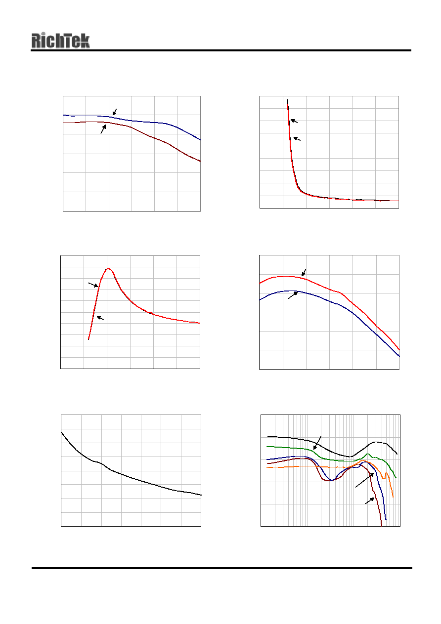
Typical Operating Characteristics
Switching Frequency vs. Temperature
460
480
500
520
540
560
580
-40
-20
0
20
40
60
80
Temperature ( C)
S
w
i
t
c
h
i
n
g Fr
eq
ue
ncy
(
KHz)
1
st
PWM
2
nd
PWM
V
DD
= 3.3V
░
Efficiency vs. Output Current
70
75
80
85
90
95
1
10
100
1000
Output Current (mA)
E
f
f
i
ci
enc
y (
%
)
V
OUT
= 3.3V
T
A
= 25
░
C
V
IN
= 3.2V
V
IN
= 2.8V
V
IN
= 2.0V
V
IN
= 2.4V
V
IN
= 1.8V
Switching Frequency vs. VDD Pin Voltage
0
100
200
300
400
500
600
700
800
900
1000
0
1
2
3
4
5
6
VDD Pin Voltage(V)
Sw
i
t
chi
n
g
Fr
equency(
K
H
z
1
st
PWM
FB1 = FB2 = GND
T
A
= 25
░
C
2
nd
PWM
)
Total Input Current (I
IN
) vs. Input Voltage
0
200
400
600
800
1000
1200
1400
1600
1.8
2.0
2.2
2.4
2.6
2.8
3.0
3.2
Input Voltage (V)
In
p
u
t C
u
rre
n
t
(
A
)
Á
V
OUT1
= 3.3V, V
OUT2
= 18V @ No Load
(Refer to Typical Application Circuit)
Feedback Voltage vs. Temperature
1.250
1.252
1.254
1.256
1.258
1.260
1.262
-40
-20
0
20
40
60
80
Temperature ( C)
F
e
ed
ba
ck V
o
l
t
a
g
e
(
V
)
.
1
st
PWM
2
nd
PWM
V
DD
= 3.3V
░
LX Pin On Resistance vs. VDD Pin Voltage
0.0
0.5
1.0
1.5
2.0
2.5
3.0
3.5
4.0
4.5
0
1
2
3
4
5
6
VDD Pin Voltage
LX
P
i
n
O
n
R
e
si
st
a
n
c
e
LX1 Pin
T
A
= 25
░
C
LX2 Pin
(V)
(
)
RT9267
Preliminary
www.richtek.com
DS9267-02 September, 2002
6
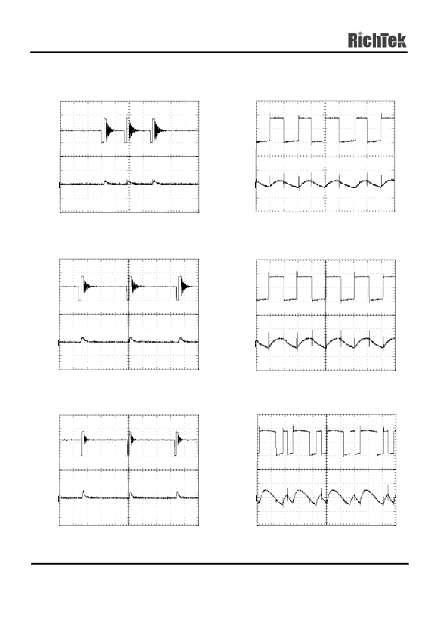
LX Pin Wave Form & Output Ripple
Time (
Á
S)
0 5 10 15 20 25 30 35 40 45 50
V
IN
= 1.8V, V
OUT
= 3.3V@ 10mA
LX Wave Form (V)
6
4
2
0
200
0
-200
Output Ripp
l
e (mV)
LX Pin Wave Form & Output Ripple
Time (
Á
S)
0 1 2 3 4 5 6 7 8 9 10
V
IN
= 1.8V, V
OUT
= 3.3V@ 200mA
LX Wave Form (V)
6
4
2
0
200
0
-200
Output Ripp
l
e (mV)
LX Pin Wave Form & Output Ripple
Time (
Á
S)
0 5 10 15 20 25 30 35 40 45 50
V
IN
= 2.0V, V
OUT
= 3.3V@ 10mA
LX Wave Form (V)
6
4
2
0
200
0
-200
Output Ripp
l
e (mV)
LX Pin Wave Form & Output Ripple
Time (
Á
S)
0 1 2 3 4 5 6 7 8 9 10
V
IN
= 2.0V, V
OUT
= 3.3V@ 300mA
LX Wave Form (V)
6
4
2
0
200
0
-200
Output Ripp
l
e (mV)
LX Pin Wave Form & Output Ripple
Time (
Á
S)
0 10 20 30 40 50 60 70 80 90 100
V
IN
= 2.4V, V
OUT
= 3.3V@ 10mA
LX Wave Form (V)
6
4
2
0
200
0
-200
Output Ripp
l
e (mV)
LX Pin Wave Form & Output Ripple
Time (
Á
S)
0 2.5 5.0 7.5 10 12.5 15 17.5 20 22.5 25
V
IN
= 2.4V, V
OUT
= 3.3V@ 550mA
LX Wave Form (V)
6
4
2
0
200
0
-200
Output Ripp
l
e (mV)

Preliminary
RT9267
DS9267-02 September, 2002
www.richtek.com
7
LX Pin Wave Form & Output Ripple
Time (
Á
S)
0 25 50 75 100 125 150 175 200 225 250
V
IN
= 2.8V, V
OUT
= 3.3V@ 10mA
LX Wave Form (V)
6
4
2
0
200
0
-200
Output Ripp
l
e (mV)
LX Pin Wave Form & Output Ripple
Time (
Á
S)
0 2.5 5.0 7.5 10 12.5 15 17.5 20 22.5 25
V
IN
= 2.8V, V
OUT
= 3.3V@ 300mA
LX Wave Form (V)
6
4
2
0
200
0
-200
Output Ripp
l
e (mV)
LX Pin Wave Form & Output Ripple
Time (
Á
S)
0 50 100 150 200 250 300 350 400 450 500
V
IN
= 3.2V, V
OUT
= 3.3V@ 10mA
LX Wave Form (V)
6
4
2
0
200
0
-200
Output Ripp
l
e (mV)
LX Pin Wave Form & Output Ripple
Time (
Á
S)
0 2.5 5.0 7.5 10 12.5 15 17.5 20 22.5 25
V
IN
= 3.2V, V
OUT
= 3.3V@ 300mA
LX Wave Form (V)
6
4
2
0
200
0
-200
Output Ripp
l
e (mV)
Transient Response
Time (250
Á
S/Div)
V
IN
= 2V, V
OUT
= 3.3V
I
OUT
= 10mA ~ 300mA
150
100
50
0
400
200
0
Output Current (mA)
Output T
r
ansient
Voltag
e (mV)
Transient Response
Time (250
Á
S/Div)
V
IN
= 3V, V
OUT
= 3.3V
I
OUT
= 10mA ~ 300mA
300
200
100
0
400
200
0
Output Current (mA)
Output T
r
ansient
Voltag
e (mV)

RT9267
Preliminary
www.richtek.com
DS9267-02 September, 2002
8
LDO Transient Response
Time (mS)
0 2.5 5 7.5 10 12.5 15 17.5 20 22.5 25
V
IN
= 2V, V
OUT
= 2.5V
I
OUT
= 10mA ~ 100mA
400
200
0
-200
100
50
0
Output Current (mA)
Output T
r
ansient
Voltag
e (mV)
LDO Transient Response
Time (mS)
0 2.5 5 7.5 10 12.5 15 17.5 20 22.5 25
V
IN
= 3V, V
OUT
= 2.5V
I
OUT
= 10mA ~ 100mA
400
200
0
-200
100
50
0
Output Current (mA)
Output T
r
ansient
Voltag
e (mV)
LDO Dropout Voltage vs. Output Current
0
50
100
150
200
250
300
350
0
50
100
150
200
250
300
Output current (mA)
L
D
O
D
r
op
out
V
o
l
t
age
(
m
V
)
.
V
DD
= 3.3V
LDOO = 2.5V
T
A
= 25
░
C
Preliminary
RT9267
DS9267-02 September, 2002
www.richtek.com
9
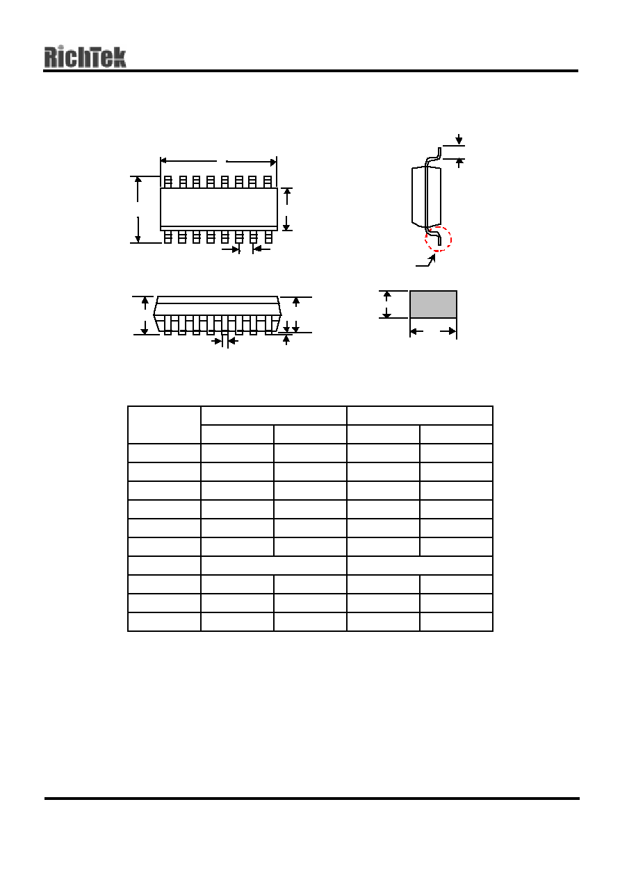
Package Information
Dimensions In Millimeters
Dimensions In Inches
Symbol
Min
Max
Min
Max
A
--
1.20
--
0.047
A1
0.05
0.15
0.002
0.006
A2
0.80
1.05
0.031
0.041
b
0.19
0.30
0.007
0.012
c
0.09
0.20
0.003
0.008
D
4.90
5.10
0.193
0.201
e
0.65
0.026
E
6.20
6.60
0.244
0.260
E1
4.30
4.50
0.169
0.177
L
0.45
0.75
0.018
0.030
16şLead TSSOP Plastic Package
L
c
VIEW A
b
SEE VIEW A
E1
E
D
e
A
b
A1
A2

RT9267
Preliminary
www.richtek.com
DS9267-02 September, 2002
10
RICHTEK TECHNOLOGY CORP.
Headquarter
5F, No. 20, Taiyuen Street, Chupei City
Hsinchu, Taiwan, R.O.C.
Tel: (8863)5526789 Fax: (8863)5526611
RICHTEK TECHNOLOGY CORP.
Taipei Office (Marketing)
8F-1, No. 137, Lane 235, Paochiao Road, Hsintien City
Taipei County, Taiwan, R.O.C.
Tel: (8862)89191466 Fax: (8862)89191465
Email: marketing@richtek.com