2-677
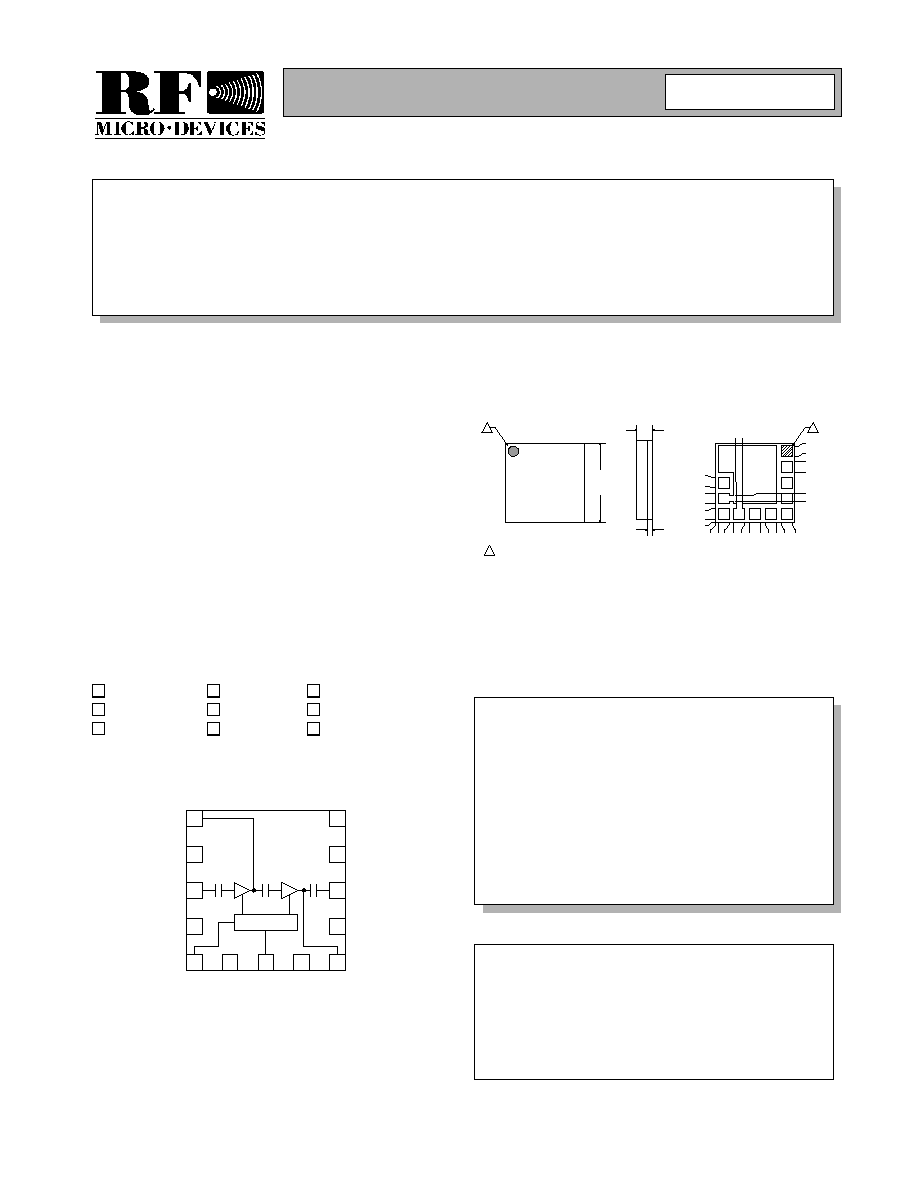
Product Description
Ordering Information
Typical Applications
Features
Functional Block Diagram
RF Micro Devices, Inc.
7628 Thorndike Road
Greensboro, NC 27409, USA
Tel (336) 664 1233
Fax (336) 664 0454
http://www.rfmd.com
Optimum Technology Matching« Applied
Si BJT
GaAs MESFET
GaAs HBT
Si Bi-CMOS
SiGe HBT
Si CMOS
InGaP/HBT
GaN HEMT
SiGe Bi-CMOS
hat is the
VREG
GND
VCC1
RF OUT
GND
VCC2
VM
O
D
E
1
2
3
4
5
6
7
8
10
9
12
11
13
Bias
GND
RF IN
GND
GND
GND
GND
RF6000-2
3V 900MHZ LINEAR AMPLIFIER MODULE
À 3V CDMA/AMPS Cellular Handsets
À 3V CDMA2000/1X Cellular Handsets
À Spread-Spectrum Systems
À Designed for Compatibility with Qualcomm
Chipsets
The RF6000-2 is a high-power, high-efficiency linear
amplifier module targeting 3V handheld systems. The
device is manufactured on a RF Micro Devices' advanced
third generation Gallium Arsenide Heterojunction Bipolar
Transistor (HBT) process, and has been designed for use
as the final RF amplifier in dual-mode 3V CDMA/AMPS
handheld digital cellular equipment, spread-spectrum
systems, and other applications in the 824MHz to
849MHz band. The RF6000-2 has a digital control line for
low power application to reduce the current drain. The
device is self-contained with 50
input and output that is
matched to obtain optimum power, efficiency, and linear-
ity characteristics. The module is an ultra-small
5mmx5mm land grid array with backside ground.
À Advanced 3rd Generation HBT Process
À Input/Output Internally Matched@50
À 28.5dBm Linear Output Power
À 29dB Linear Gain
À 45mA Idle Current (Low Power Mode)
À CDMA2000 Compatible
RF6000-2
3V 900MHz Linear Amplifier Module
RF6000-2 PCBA Fully Assembled Evaluation Board
0
Rev A2 021218
Bottom View
1.70
1.45
0.450
▒ 0.075
Dimensions in mm.
5.00
▒ 0.10
sq.
1
0.150 TYP
0.000
1.150 TYP
1.850 TYP
2.150 TYP
2.850 TYP
3.850
4.150
0.1
50 T
Y
P
0.0
0
0
0.8
50 T
Y
P
1.1
50 T
Y
P
2.8
5
0
2.1
5
0
1.8
5
0
3.1
5
0
3.8
50 T
Y
P
4.1
50 T
Y
P
4.8
50 T
Y
P
1
4.850 TYP
3.150 TYP
1.325
1.675
1
.
675
1.32
5
0.850 TYP
Shaded areas represent pin 1 location.
1
Package Style: LGM (5mmx5mm)
Preliminary
!
Preliminary
2-678
RF6000-2
Rev A2 021218
Absolute Maximum Ratings
Parameter
Rating
Unit
Supply Voltage (RF off)
+8.0
V
DC
Supply Voltage (P
OUT
31dBm)
+5.2
V
DC
Control Voltage (V
REG
)
+4.2
V
DC
Input RF Power
+10
dBm
Mode Voltage (V
MODE
)
+3.5
V
DC
Operating Case Temperature
-30 to +110
░C
Storage Temperature
-30 to +150
░C
Parameter
Specification
Unit
Condition
Min.
Typ.
Max.
High Power State
(V
MODE
Low)
Typical Performance at V
CC
=3.4V,
V
REG
=2.85V, T
AMB
=25░C,
Frequency=836MHz
(unless otherwise specified)
Frequency Range
824
849
MHz
Linear Gain
29
dB
Second Harmonic
-35
dBc
Third Harmonic
-35
dBc
Maximum Linear Output Power
28
28.5
dBm
Low Voltage Linear Output
Power
27
dBm
V
CC
=3.0V
Total Linear Efficiency
38
%
P
OUT
=28.5dBm (room temperature)
Total I
CC
530
mA
P
OUT
=28dBm
Adjacent Channel Power
Rejection
-50
-46
dBc
ACPR@885kHz. P
OUT
=28dBm (IS-95)
-61
-58
dBc
ACPR@1980kHz. P
OUT
=28dBm (IS-95)
Input VSWR
2:1
Output VSWR
10:1
No damage.
6:1
No oscillations. >-70dBc
Noise Power
-136
dBm/Hz
At 45MHz offset.
Low Power State
(V
MODE
High)
Typical Performance at V
CC
=3.4V,
V
REG
=2.85V, T
AMB
=25░C,
Frequency=836MHz
(unless otherwise specified)
Frequency Range
824
849
MHz
Linear Gain
20
dB
Second Harmonic
-35
dBc
Third Harmonic
-35
dBc
Maximum Linear Output Power
18
20
dBm
Total Current, I
CC
180
mA
P
OUT
=18dBm
Adjacent Channel Power
Rejection
-50
-46
dBc
ACPR@885kHz. P
OUT
=18dBm (IS-95)
-70
-58
dBc
ACPR@1980kHz. P
OUT
=18dBm (IS-95)
Input VSWR
2:1
Output VSWR
10:1
No damage.
6:1
No oscillations. >-70dBc
Caution! ESD sensitive device.
RF Micro Devices believes the furnished information is correct and accurate
at the time of this printing. However, RF Micro Devices reserves the right to
make changes to its products without notice. RF Micro Devices does not
assume responsibility for the use of the described product(s).

Preliminary
2-679
RF6000-2
Rev A2 021218
CDMA2000 Configuration Table
Parameter
Specification
Unit
Condition
Min.
Typ.
Max.
FM Mode
Typical Performance at V
CC
=3.4V,
V
REG
=2.85V, T
AMB
=25░C,
Frequency=836MHz
(unless otherwise specified)
Frequency Range
824
849
MHz
Gain
28
dB
Second Harmonic
-35
dBc
Third Harmonic
-35
dBc
Max CW Output Power
31.5
dBm
Total Efficiency (AMPS mode)
48
%
V
CC
=3.4V, V
REG
=2.85V, P
OUT
=31.5dBm
(room temperature)
Input VSWR
2:1
Output VSWR
10:1
No damage.
5:1
No oscillations. >-70dBc
DC Supply
Supply Voltage Range
3.2
3.4
4.2
V
Quiescent Current
150
mA
V
MODE
=Low, V
REG
=2.85V
45
mA
V
MODE
=High, V
REG
=2.85V
V
REG
Current
3
mA
V
MODE
Current
250
Á
A
Turn On/Off Time
<40
Á
s
V
REG
switch from Low to High,
I
CC
to within 90% of the final value,
P
OUT
within 1dB of the final value
Total Current (Power Down)
5
Á
A
V
REG
=Low, V
MODE
=Low
V
REG
"Low" Voltage
0
0.5
V
V
REG
"High" Voltage
2.8
2.85
2.9
V
V
MODE
"Low" Voltage
0
0.5
V
V
MODE
"High" Voltage
2.0
3.0
V
Relative Gains
No.
Configuration
Peak-to-Average
CCDF=1%
PCH
DCCH
FCH
SCH
Typical Maximum
Output Power (dBm)
1
DCCH 9600
5.4
-3.75
0
26.5
2
FCH 9600, SCH0 9600
4.5
-3.75
0
0
28.0
3
DCCH 9600, SCH0 9600
4.5
-3.75
0
0
28.0
4
FCH 9600, SCH0 19200
4.5
-6.25
-2.65
0
28.0
5
FCH 9600, SCH0 38400
4.3
-7.5
-5.125
0
28.0
6
DCCH 9600, SCH0 19200
4.1
-6.25
-2.65
0
28.0
7
RC1 (IS-95 Reference)
3.9
28.0
8
FCH 9600, SCH0 76800
3.9
-9.0
-7.875
0
28.0
9
DCCH 9600, SCH0 38400
3.9
-7.5
-5.125
0
28.0
10
DCCH 9600, SCH0 76800
3.6
-9.0
-7.875
0
28.0
11
FCH 9600
3.2
-3.75
0
28.0
12
FCH 1500
3.2
0
-5.875
28.0
13
FCH 2700
3.2
0
-2.75
28.0
14
FCH 4800
3.2
0
-0.25
28.0
15
Pilot Only
3.2
0
28.0

Preliminary
2-680
RF6000-2
Rev A2 021218
Pin
Function
Description
Interface Schematic
1
VCC1
First stage collector supply. A low frequency decoupling capacitor
(e.g., 4.7
Á
F) is required.
2
GND
Ground connection. Connect to package base ground. For best perfor-
mance, keep traces physically short and connect immediately to
ground plane.
3
RF IN
RF input internally matched to 50
. This input is internally AC-coupled.
4
GND
Ground connection. Connect to package base ground. For best perfor-
mance, keep traces physically short and connect immediately to
ground plane.
5
VREG
Regulated voltage supply for amplifier bias. In Power Down mode, both
V
REG
and V
MODE
need to be LOW (<0.5V).
6
GND
Ground connection. Connect to package base ground. For best perfor-
mance, keep traces physically short and connect immediately to
ground plane.
7
VMODE
For nominal operation (High Power Mode), V
MODE
is set LOW. When
set HIGH, devices are turned off to improve efficiency.
8
GND
Ground connection. Connect to package base ground. For best perfor-
mance, keep traces physically short and connect immediately to
ground plane.
9
VCC2
Output stage collector supply. A low frequency decoupling capacitor
(e.g., 22
Á
F) is required.
10
GND
Ground connection. Connect to package base ground. For best perfor-
mance, keep traces physically short and connect immediately to
ground plane.
11
RF OUT
RF output internally matched to 50
. This output is internally
AC-coupled.
12
GND
Ground connection. Connect to package base ground. For best perfor-
mance, keep traces physically short and connect immediately to
ground plane.
13
GND
Ground connection. Connect to package base ground. For best perfor-
mance, keep traces physically short and connect immediately to
ground plane.
Pkg
Base
GND
Ground connection. The backside of the package should be soldered to
a top side ground pad which is connected to the ground plane with mul-
tiple vias. The pad should have a short thermal path to the ground
plane.

Preliminary
2-681
RF6000-2
Rev A2 021218
Evaluation Board Schematic
(Download Bill of Materials from www.rfmd.com.)
1
2
3
4
5
6
7
8
10
9
12
11
13
Bias
VCC1
C2
4.7
Á
F
50
Á
strip
J2
RF OUT
50
Á
strip
J1
RF IN
VREG
C4
4.7
Á
F
VMODE
C3
4.7
Á
F
VCC2
C1
22
Á
F
Preliminary
2-682
RF6000-2
Rev A2 021218
Evaluation Board Layout
Board Size 1.0" x 1.5"
Board Thickness 0.042", Board Material RO4003, Ground plane at 0.020", Multi-layer