M5M29KB/T331AVP
Renesas LSIs
Rev.1.0_48a_bezz
1
33,554,432-BIT (4,194,304-WORD BY 8-BIT /2,097,152-WORD BY 16-BIT)
CMOS 3.3V-ONLY, BLOCK ERASE FLASH MEMORY
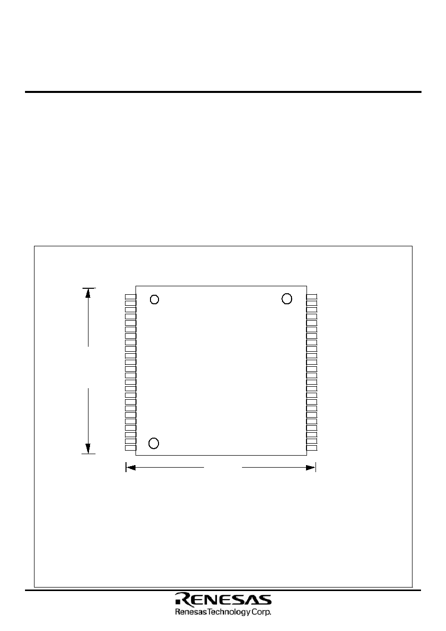
PIN CONFIGURATION (TOP VIEW)
Outline
48P3R-C
Digital Cellar Phone, Telecommunication,
PDA, Car Navigation System, Video Game Machine
1
2
3
4
5
6
7
8
9
10
11
12
13
14
15
16
17
18
19
20
21
22
23
48
47
46
45
44
43
42
41
40
39
38
37
36
35
34
33
32
31
30
29
A15
A14
A13
A12
A11
A10
A9
A8
A19
A20
WE#
RP#
NC
RY/BY#
A18
A17
A7
A6
A5
A4
A3
A16
BYTE#
GND
DQ15/A-1
DQ7
DQ14
DQ6
DQ13
DQ5
DQ12
DQ4
VCC
DQ11
DQ3
DQ10
DQ2
DQ9
DQ1
DQ8
DQ0
OE#
GND
28
25
A0
24
A2
A1
20.0 mm
12.0
mm
WP#
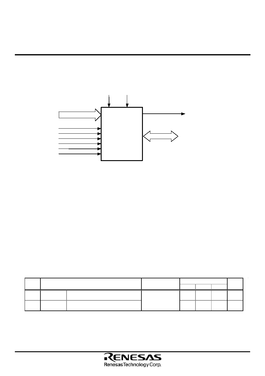
DESCRIPTION
FEATURES
Access time
Random
70ns (Max.)
Page
25ns(Max.)
Supply voltage
VCC= 3.0 ~ 3.6V
Ambient temperature
Ta=-40 ~ 85
�
C
Package
48pin TSOP(Type-I), Lead pitch 0.5mm
Outer-lead finishing : Sn-Cu
APPLICATION
VCC
: VCC
GND
: GND
A0-A21
: Address
DQ0-DQ15
: Data I/O
CE#
: Chip enable
OE#
: Output enable
WE#
: Write enable
WP#
: Write protect
RP#
: Reset power down
BYTE#
: Byte enable
RY/BY#
: Ready/Busy
NC
: Non Connection
CE#
The M5M29KB/T331AVP are 3.3V-only high speed
33,554,432-bit CMOS boot block FLASH Memories with
alternating BGO(Back Ground Operation) feature. The BGO
feature of the device allows Program or Erase operations to be
performed in one bank while the device simultaneously allows
Read operations to be performed on the other bank.
This BGO feature is suitable for mobile and personal
computing, and communication products.
The M5M29KB/T331AVP are fabricated by CMOS technology
for the peripheral circuit and DINOR IV(Divided bit-line NOR IV)
architecture for the memory cell, and are available in 48pin
TSOP(I) for lead free use.
M5M29KB/T331AVP provides for Software Lock Release
function. Usually, all memory blocks are locked and can not
be programmed or erased, when WP# is low. Using Software
Lock Release function, program or erase operation can be
executed.
27
26
M5M29KB/T331AVP

M5M29KB/T331AVP
Renesas LSIs
Rev.1.0_48a_bezz
3
33,554,432-BIT (4,194,304-WORD BY 8-BIT /2,097,152-WORD BY 16-BIT)
CMOS 3.3V-ONLY, BLOCK ERASE FLASH MEMORY
The 32M-bit DINOR IV(Divided bit line NOR IV) Flash
Memory is 3.3V-only high speed 33,554,432-bit CMOS
boot block Flash Memory. Alternating BGO(Back Ground
Operation) feature of the device allows Program or Erase
operations to be performed in one bank while the device
simultaneously allows Read operations to be performed
on the other bank. This BGO feature is suitable for
communication products and cellular phone.The Flash
Memory is fabricated by CMOS technology for the
peripheral circuits and DINOR IV architecture for the
memory cells.
Features
-Organization
2,097,152-word x 16-bit
4,194,304-byte x 8-bit
- Supply Voltage
VCC = 3.0
~
3.6V
- Access time
Random Access
70ns(Max.)
Random Page Read
25ns(Max.)
- Read
108mW (Max. at 5MHz)
- Page Read
36mW (Max.)
(After Automatic Power Down)
0.33�W(typ.)
- Program/Erase
126mW(Max.)
Standby
0. 33�W(typ.)
Deep Power Down mode
0. 33�W(typ.)
- Auto Program for Bank(I) � Bank(IV)
Program Time
Word Program
30�s/word(typ.)
Byte Program
30�s/byte(typ.)
Page Program
4ms(typ.)
Program Unit
Word/Byte Program
1word/ 1Byte
Page Program
128 words/ 256 bytes
- Auto Erase
Erase time
Main Block
150ms/block (typ.)
Erase unit
Bank(I)
Boot Block
4K-word x2/ 8K-byte x2
Parameter Block 4K-word x6 / 8K-byte x6
Main Block
32K-word x7 / 64K-byte x7
Bank(II)
Main Block
32K-word x8 / 64K-byte x8
Bank(III)
Main Block
32K-word x24 / 64K-byte x24
Bank(IV)
Main Block
32K-word x24 / 64K-byte x24
- Program/Erase cycles
100Kcycles
- Boot Block
Bottom Boot
M***B33******
Top Boot
M***T33******
- The Other Functions
Software Command Control
Software Lock Release(while WP# is low)
Erase Suspend/Resume
Program Suspend/Resume
Status Register Read
Alternating Back Ground Program/Erase Operation
Between Bank(I), Bank(II), Bank(III) and Bank(IV)
Random Page Read
Flash Memory Part
Description

M5M29KB/T331AVP
Renesas LSIs
Rev.1.0_48a_bezz
4
33,554,432-BIT (4,194,304-WORD BY 8-BIT /2,097,152-WORD BY 16-BIT)
CMOS 3.3V-ONLY, BLOCK ERASE FLASH MEMORY
Block Diagram (32Mbit Flash Memory)
�
Main Block 70 32Kword
�
�
�
�
�
�
�
Bank(IV)
�
�
24blocks
�
�
�
�
�
�
�
�
�
�
�
�
�
�
Main Block 47 32Kword
�
Main Block 46 32Kword
�
�
�
�
�
�
�
Bank(III)
�
24blocks
�
�
�
�
�
�
�
�
�
�
�
�
�
Main Block 23 32Kword
�
Main Block 22 32Kword
�
Bank(II)
�
�
8blocks
�
�
�
�
Main Block 15 32Kword
�
Main Block 14 32Kword
�
�
�
Main Block 8 32Kword
�
Bank(I)
Parameter Block 7 4Kword
�
15blocks
�
�
Parameter Block 2 4Kword
�
Boot Block 1 4Kword
Boot Block 0 4Kword
�
�
�
�
�
Write
Protect
BYTE
I/O Buffer
� � � � � � � � � � � � � � � � � � � � � � � � � � �
Chip
Enable
� � � � � � � � � � � � � � � � � � � � � � � � � � �
Reset
/PowerDown
Output Enable
Write Enable
Command
User
Interface
Write
State
Machine
� � � � � � � � � � � � � � � � � � � � � � � � � � �
Status / ID Register
Multiplexer
� � � � � � � � � � � � � � � � � � � � � � � � � � �
X-Decoder
Address
Input
Y-Decoder
Y-Gate / Sense Amp.
128word Page Buffer
A20
A19
A18
A17
A16
A15
A14
A13
A12
A11
A10
A9
A8
A7
A6
A5
A4
A3
A2
A1
A0
OE#
WE#
WP#
RP#
CE#
VCC
GND
BYTE#
DQ0
DQ1
DQ15
/ A-1
DQ14
Data I/O
RY/
BY#
READY/BUSY
Data I/O

M5M29KB/T331AVP
Renesas LSIs
Rev.1.0_48a_bezz
5
33,554,432-BIT (4,194,304-WORD BY 8-BIT /2,097,152-WORD BY 16-BIT)
CMOS 3.3V-ONLY, BLOCK ERASE FLASH MEMORY
When RP# is at VIL, the device is in the deep power down
mode and its power consumption is substantially low.
During read modes, the memory is deselected and the data
input/output are in a high-impedance (High-Z) state. After
return from power down, the CUI is reset to Read Array,
and the Status Register is cleared to value 80H.
During block erase or program modes, RP# low will abort
either operation. Memory array data of the block being
altered become invalid.
The Automatic Power Down minimizes the power
consumption during read mode. The device automatically
turns to this mode when any addresses or CE# isn't
changed more than 200ns after the last alternation. The
power consumption becomes the same as the stand-by
mode. During this mode, the output data is latched and can
be read out. New data is read out correctly when
addresses are changed.
In the 32M-bit DINOR IV Flash Memory , when one
memory address is read according to a Read Mode in the
case of the same as an access when a Read Mode
command is input, an another Bank memory data can be
read out (Random or Page Mode) by changing an another
Bank address.
When OE# is at VIH, output from the devices is disabled.
Data input/output are in a high-impedance (High-Z) state.
Output Disable
The 32M-bit DINOR IV Flash Memory includes on-chip
program/erase control circuitry. The Write State Machine
(WSM) controls block erase and word/page program
operations. Operational modes are selected by the
commands written to the Command User Interface (CUI).
The Status Register indicates the status of the WSM and
when the WSM successfully completes the desired
program or block erase operation.
A Deep Power Down mode is enabled when the RP# pin
is at GND, minimizing power consumption.
Function of Flash Memory
The 32M-bit DINOR IV Flash Memory has four read
modes, which accesses to the memory array, the Page
Read, the Device Identifier and the Status Register. The
appropriate read commands are required to be written to
the CUI. Upon initial device power up or after exit from
deep power down, the 32M-bit DINOR IV Flash Memory
automatically resets to read array mode. In the read array
mode and in the conditions are low level input to OE#,
high level input to WE# and RP#, low level input to CE#
and address signals to the address inputs (A20 - A0:
Word mode / A20-A-1: Byte mode) the data of the
addressed location to the data input/output (DQ15-DQ0:
Word mode / DQ7- DQ0: Byte mode) is output.
Read
Writes to the CUI enables reading of memory array data,
device identifiers and reading and clearing of the Status
Register. They also enable block erase and program. The
CUI is written by bringing WE# to low level and OE# is at
high level, while CE# is at low level. Address and data are
latched on the earlier rising edge of WE# and CE#.
Standard micro processor write timings are used.
Write
The 32M-bit DINOR IV Flash Memory allows to read
array from one bank while the other bank operates in
software command write cycling or the erasing /
programming operation in the background. Array Read
operation with the other bank in BGO is performed by
changing the bank address without any additional
command. When the bank address points the bank in
software command write cycling or the erasing /
programming operation, the data is read out from the
status register. The access time with BGO is the same as
the normal read operation. BGO must be between Bank(I),
Bank(II), Bank(III) and Bank(IV).
When CE# is at VIH, the device is in the standby mode
and its power consumption is reduced. Data input/output
are in a high-impedance (High-Z) state. If the memory is
deselected during block erase or program, the internal
control circuits remain active and the device consumes
normal active power until the operation completes.
Standby
Alternating Background Operation (BGO)
Read
Deep Power Down
BBR(Back Bank array Read)
Automatic Power Down (Auto-PD)