
SMSC DS SLC90E66
Rev. 07/10/2002
SLC90E66
PRELIMINARY
Victory66 Enhanced PCI South Bridge with Ultra
ATA/66 IDE Controller
FEATURES
§
Enhanced PCI South Bridge for Desktop, Mobile
and Embedded Applications
-
Pin Compatible with Intel 82371EB PIIX4E
South Bridge
-
High Performance OHCI USB Host Controller
-
Ultra ATA/66 IDE Controller
-
Enhanced Support for Mobile Applications
-
Compatible with Full Line of Intel PCI-based
North Bridge Devices
-
Programmable Support for Third Party North
Bridge Solutions
§
Supported Kits for Pentium
®
II and Pentium
®
III
Microprocessors
-
VictoryBX-66 Chipset with Intel FW82443BX
(440BX) North Bridge
§
Integrated Ultra ATA/66 IDE Controller
-
Supports "Ultra ATA/66" Synchronous DMA
Modes with Transfer Rate up to
66Mbytes/Second
-
Independent Timing for up to Four Drives
-
Supports PIO Mode 0 to 4, Multiword DMA
Mode 0, 1 and 2
-
Integrated 32x32-bit Buffer For Each Channel
-
Supports Glue-Less "Swap-Bay" Option with
Full Electrical Isolation
-
Supports Both Legacy and PCI-Native Modes
§
Enhanced OHCI USB Host Controller
-
Two USB 1.0 Ports for Serial Transfers at 12 or
1.5Mbit/Sec
-
Supports Legacy Keyboard and Mouse
Software with USB Keyboard and Mouse
-
Supports Wakeup From Power-on Suspend
§
Integrated Multifunction PCI-To-ISA Bridge
-
Supports PCI up to 33 MHz
-
Supports PCI Rev 2.1 Specification
-
Programmable Special Cycle Support for
Compatibility with Non-Intel North Bridges
-
Supports Full ISA or Extended I/O (EIO) Bus
-
Supports Full Positive Decode or Subtractive
Decode of PCI
-
Supports ISA/EIO At Ľ of PCI Frequency
§
Comprehensive BIOS support
§
Comprehensive Power Management Capability
for Mobile and Desktop Applications
-
3.3V Operation with 5V Tolerent Buffers
-
Low Power for Mobile Applications
-
Supports Power-On Suspend and Soft-Off for
Desktop Applications
-
Comprehensive Suspend/Resume Logic for
Notebook Applications
-
All Registers Readable/Restorable For Proper
Resume From 0V Suspend
-
Global and Local Device Management
-
Supports Thermal Alarm
-
Support For External Microcontroller
-
Full Support of Advanced Configuration and
Power Interface (ACPI) Rev. 1.0 Specification
and OS Directed Power Management
-
Supports PCI CLKRUN Protocol
§
Enhanced DMA Controller
-
Two 8237 DMA Controllers
-
Supports PCI DMA with 3 PC/PCI Channels
and Distributed DMA Protocols
-
Supports Type-F DMA with Deep 4-DW Buffer
§
Interrupt
Controller
-
Two 8259 Interrupt Controllers
-
Independently Programmable Edge/Level
Sensitivity
-
Supports Serial Interrupt
-
Supports Optional External I/O APIC
§
Integrated
8254
Timer
-
System Timer, Refresh Request, Speaker
Tone Output
§
Integrated SMBus Host Controller
-
Host Allows CPU to Communicate Via SMBus
-
Slave Allows External SMBus Master to
Control Resume Events
§
Real Time Clock
-
256-Byte Battery Backup CMOS SRAM
-
Date Alarm
-
Two 8-Byte Lockout Ranges
-
Relocatable RTC Index Base Address
-
Can Be Disabled for Use With External RTC
§
324-ball Plastic Ball Grid Array (PBGA) Package

SMSC DS SLC90E66
Page 2
Rev. 07/10/2002
© STANDARD MICROSYSTEMS CORPORATION (SMSC) 2002
80 Arkay Drive
Hauppauge, NY 11788
(631) 435-6000
FAX (631) 273-3123
Standard Microsystems is a registered trademark of Standard Microsystems Corporation, and SMSC is a trademark of Standard Microsystems
Corporation. Pentium is a registered trademark of Intel Corporation. Product names and company names are the trademarks of their respective
holders. Circuit diagrams utilizing SMSC products are included as a means of illustrating typical applications; consequently complete information
sufficient for construction purposes is not necessarily given. Although the information has been checked and is believed to be accurate, no
responsibility is assumed for inaccuracies. SMSC reserves the right to make changes to specifications and product descriptions at any time without
notice. Contact your local SMSC sales office to obtain the latest specifications before placing your product order. The provision of this information does
not convey to the purchaser of the semiconductor devices described any licenses under the patent rights of SMSC or others. All sales are expressly
conditional on your agreement to the terms and conditions of the most recently dated version of SMSC's standard Terms of Sale Agreement dated
before the date of your order (the "Terms of Sale Agreement"). The product may contain design defects or errors known as anomalies which may
cause the product's functions to deviate from published specifications. Anomaly sheets are available upon request. SMSC products are not designed,
intended, authorized or warranted for use in any life support or other application where product failure could cause or contribute to personal injury or
severe property damage. Any and all such uses without prior written approval of an Officer of SMSC and further testing and/or modification will be fully
at the risk of the customer. Copies of this document or other SMSC literature, as well as the Terms of Sale Agreement, may be obtained by visiting
SMSC's website at http://www.smsc.com.
SMSC DISCLAIMS AND EXCLUDES ANY AND ALL WARRANTIES, INCLUDING WITHOUT LIMITATION ANY AND ALL IMPLIED WARRANTIES
OF MERCHANTABILITY, FITNESS FOR A PARTICULAR PURPOSE, TITLE, AND AGAINST INFRINGEMENT, AND ANY AND ALL
WARRANTIES ARISING FROM ANY COURSE OF DEALING OR USAGE OF TRADE.
IN NO EVENT SHALL SMSC BE LIABLE FOR ANY DIRECT, INCIDENTAL, INDIRECT, SPECIAL, PUNITIVE, OR CONSEQUENTIAL DAMAGES,
OR FOR LOST DATA, PROFITS, SAVINGS OR REVENUES OF ANY KIND; REGARDLESS OF THE FORM OF ACTION, WHETHER BASED ON
CONTRACT, TORT, NEGLIGENCE OF SMSC OR OTHERS, STRICT LIABILITY, BREACH OF WARRANTY, OR OTHERWISE; WHETHER OR
NOT ANY REMEDY IS HELD TO HAVE FAILED OF ITS ESSENTIAL PURPOSE; AND WHETHER OR NOT SMSC HAS BEEN ADVISED OF THE
POSSIBILITY OF SUCH DAMAGES.

SMSC DS SLC90E66
Page 3
Rev. 07/10/2002
GENERAL DESCRIPTION
The Victory66 SLC90E66 Enhanced PCI South Bridge with Ultra ATA/66MHz IDE Controller is a multi-function PCI
device implementing a PCI-to-ISA bridge function, a PCI Ultra ATA/66 IDE controller function, a Universal Serial Bus
host/hub function, and an Enhanced Power Management function. As a PCI-to-ISA bridge, the SLC90E66 integrates
I/O functions found in a common ISA bridge chip, that includes two DMA controllers, two interrupt controllers, an 8254
timer, and a Real Time Clock. The DMA controllers support Type-F data transfers on each of the eight channels. The
SLC90E66 also supports PC/PCI and Distributed DMA protocols for PCI based DMA applications. The Interrupt
Controllers support Edge or Level sensitive programmable inputs and the use of an external I/O APIC and serial
interrupts. The SLC90E66 can be configured to provide chip select decoding for BIOS, RTC, keyboard controller,
external microcontroller, and two programmable chip selects. The SLC90E66 can be configured as a subtractive
decode bridge or as a positive decode bridge. This allows the use of a subtractive decode PCI-to-PCI bridge such as
that used in a PCI/ISA docking station environment.
The SLC90E66 supports two IDE channels for up to four IDE devices in either PIO or Bus Master mode. The
SLC90E66 also supports "Ultra ATA/66" synchronous DMA compatible devices for data transfer rates up to 66Mbytes
per second. The embedded 32 double word (32x32-bit)deep buffers allow zero wait state PCI burst transfer in either
direction.
The SLC90E66 integrates a USB host controller that is Open Host Controller Interface (OHCI) compatible. Two USB
ports are implemented in the root hub. The USB controller has been enhanced to support wake-up from a power-on
suspend (POS).
The SLC90E66 supports comprehensive power management, including full clock control, device power management
for up to 14 devices, global power management and suspend and resume logic with Power On Suspend, Suspend to
RAM or Suspend to Disk. It fully supports operating system directed power management via the Advanced
Configuration and Power Interface (ACPI) specification. System Management Bus (SMBus) host and slave interface
logic is integrated for communication with other on-board devices.
ORDERING INFORMATION
Order Number:
SLC90E66-UF
324-Ball BGA Package

SMSC DS SLC90E66
Page 4
Rev. 07/10/2002
SLC90E66 SIMPLIFIED BLOCK DIAGRAM
u
Secondary
IDE
Interface
ISA
Bus
Interface
SD[15:0]
SA[19:0]
LA[23:17]
nIOCS16
nMEMCS16
nMEMW
nMEMR
nIOW
nIOR
AEN
BALE
IOCHRDY
nIOCHK
SYSCLK
nSMEMW
nSMEMR
nZEROWS
nSBHE
PCI BUS
Interface
PCICLK
AD[31:0]
C/nBE[3:0]
nFRAME
nIRDY
nTRDY
nSTOP
nDEVSEL
nIDSEL
nSERR
PAR
nPHOLD
nPHLDA
nCLKRUN
System
Reset
PCIRST
PWROK
nRCIN
CPURST
RSTDRV
INIT
Primary
IDE
Interface
PIORDY
nPDCS1
nPDCS3
PDA[2:0]
PDD[15:0]
nPDIOW
nPDIOR
PDDREQ
nPDDACK
nPCBLID
SIORDY
nSDCS1
nSDCS3
SDA[2:0]
SDD[15:0]
nSDIOW
nSDIOR
SDDREQ
nSDDACK
nSCBLID
USB
Interface
nOC[1:0]
CLK48
USBP0[+:-]
USBP1[+:-]
Power
Mgmt
Logic
nSMI
nSTPCLK
nEXTSMI
SUSCLK
nCPU_STP
nPCI_STP
nBATLOW
nTHRM
LID
nRI
nRSMRST
nPWRBTN
nSUS[A:C]
nSUS_STAT[2:1]
ZZ
nPIRQ[A:D]
nSLP
nXDIR
nA20M
A20GATE
nFERR
nIGNNE
nXOE
nRTCCS
RTCALE
nKBCCS
nMCCS
nBIOSCS
nPCS[1:0]
XBus
Interface
Logic
IRQ0
nIRQ8
IRQ12/M
INTR
NMI
IRQ[15,14,11:9,7:3,1]
SERIRQ
nPIRQ[A:C]
nPIRQ[D]
Interrupt
Logic
I/O APIC
Interface
nAPICREQ
nAPICACK
nAPICCS
nIRQ9OUT/GPO28
DREQ[7:5,3:0]
nDACK[7:5,3:0]
TC
nREFRESH
nREQ[A:C]
nGNT[A:C]
DMA
Logic
OSC
SPKR
Timer
RTCX[2:1]
RTC
XOSCSEL
GPIO
GPOx
GPIX
Test
CONFIG[2:1]
nTEST
SMBDATA
nSMBALERT
SMBCLK
SMBus
Interface

SMSC DS SLC90E66
Page 5
Rev. 07/10/2002
TABLE OF CONTENTS
1.0
FUNCTIONAL OVERVIEW ............................................................................................................................. 13
2.0
SIGNAL DESCRIPTION.................................................................................................................................. 16
2.1
S
IGNALS
........................................................................................................................................................ 17
2.1.1
PCI Bus Interface ................................................................................................................................ 17
2.1.2
ISA/EIO Interface Signals .................................................................................................................... 19
2.1.3
Xbus Interface Signals........................................................................................................................ 22
2.1.4
DMA Signals........................................................................................................................................ 23
2.1.5
Interrupt Controller and APIC Signals.................................................................................................. 24
2.1.6
CPU Interface Signals ......................................................................................................................... 25
2.1.7
Clocks.................................................................................................................................................. 27
2.1.8
IDE Signals.......................................................................................................................................... 28
2.1.9
Universal Serial Bus Signals................................................................................................................ 32
2.1.10
Power Management Signals................................................................................................................ 32
2.1.11
General Purpose Input and Output Signals ......................................................................................... 35
2.1.12
Other System and Test Signals ........................................................................................................... 37
2.1.13
Power and Ground Pins....................................................................................................................... 37
2.2
P
OWER
P
LANES
............................................................................................................................................. 38
2.2.1
Power Sequencing Requirements ....................................................................................................... 38
3.0
REGISTER SUMMARY................................................................................................................................... 39
3.1
PCI/ISA B
RIDGE
R
EGISTER
M
APPING
.............................................................................................................. 39
3.1.1
PCI Configuration Registers (Function 0) ............................................................................................ 39
3.1.2
IO Space Registers (Function 0) ......................................................................................................... 40
3.2
IDE C
ONTROLLER
R
EGISTER
M
APPING
T
ABLE
(F
UNCTION
1) ............................................................................. 43
3.2.1
PCI Configuration Registers (Function 1) ............................................................................................ 43
3.2.2
IO Space Registers.............................................................................................................................. 44
3.3
U
NIVERSAL
S
ERIAL
B
US
(USB) C
ONTROLLER
R
EGISTER
M
APPING
T
ABLE
(F
UNCTION
2) ...................................... 44
3.3.1
PCI Configuration Registers (Function 2) ............................................................................................ 44
3.3.2
SB OpenHCI Memory Mapped Registers (Function 2)........................................................................ 45
3.4
P
OWER
M
ANAGEMENT
R
EGISTER
M
APPING
T
ABLE
(F
UNCTION
3)........................................................................ 45
3.4.1
PCI Configuration Registers (Function 3) ............................................................................................ 45
3.4.2
Power Management IO Space Registers (Function 3)......................................................................... 46
3.4.3
SMBus Controller IO Space Registers (Function 3) ............................................................................ 47
4.0
PCI/ISA BRIDGE PCI REGISTER DESCRIPTION (FUNCTION 0) ................................................................ 48
4.1
PCI/ISA B
RIDGE
PCI C
ONFIGURATION
S
PACE
R
EGISTERS
(PCI F
UNCTION
0) .................................................... 48
4.1.1
VID - Vendor Identification Register (Function 0) ................................................................................ 48
4.1.2
DID - Device Identification Register (Function 0)................................................................................. 48
4.1.3
PCICMD - PCI Command Register (Function 0) ................................................................................. 48
4.1.4
PCISTS - PCI Device Status Register (Function 0) ............................................................................. 49
4.1.5
RID - Revision ID Register (Function 0)............................................................................................... 49
4.1.6
CLASSCODE - Class Code Register (Function 0) .............................................................................. 50
4.1.7
HEDT - Header Type Register (Function 0)......................................................................................... 50
4.1.8
IORT - ISA I/O Recovery Timer Register (Function 0)......................................................................... 50
4.1.9
XBCS - X-Bus Chip Select Register (Function 0) ................................................................................ 51
4.1.10
nPIRQRC[A:D] - nPIRQx Route Control Registers (Function 0).......................................................... 53
4.1.11
SERIRQC - Serial IRQ Control Register (Function 0).......................................................................... 54
4.1.12
FDMA - Type-F DMA Control Register (Function 0) ............................................................................ 54
4.1.13
IRQ8SR - IRQ8 Source Register (Function 0) ..................................................................................... 55
4.1.14
TOM - Top of Memory Register (Function 0) ....................................................................................... 55
4.1.15
MBDMA [1:0] - Motherboard Device DMA Control Registers (Function 0) .......................................... 56
4.1.16
APICBASE - APIC Base Address Relocation Register (Function 0).................................................... 56
4.1.17
DLC - Deterministic Latency Control Register (Function 0) ................................................................. 57
4.1.18
PDMACFG - PCI DMA Configuration Register (Function 0) ................................................................ 57
4.1.19
DDMABP - Distributed DMA Slave Base Pointer Registers (Function 0)............................................. 59
4.1.20
GENCFG - General Configuration Register (Function 0)..................................................................... 59
4.1.21
RTCCFG - Real Time Clock Configuration Register (Function 0)........................................................ 62
4.1.22
RTCPBAL - RTC Index Primary Base Address Low Byte (Function 0)................................................ 63
4.1.23
RTCPBAH - RTC Index Primary Base Address High Byte (Function 0) .............................................. 63
4.1.24
SBMISCL - South Bridge Miscellaneous Low Register (Function 0) ................................................... 64

SMSC DS SLC90E66
Page 6
Rev. 07/10/2002
4.1.25
SBMISCH South Bridge Miscellaneous High Register (Function 0) .................................................... 64
4.1.26
SHUTSC - Shutdown Special Cycle Code Register (Function 0) ........................................................ 65
4.1.27
SGSC - Stop Grant Special Cycle Code Register (Function 0) ........................................................... 65
4.2
PCI
TO
ISA/EIO B
RIDGE
I/O R
EGISTERS
......................................................................................................... 65
4.2.1
DMA Registers .................................................................................................................................... 65
4.2.2
Interrupt Controller Registers (I/O)....................................................................................................... 71
4.2.3
Counter/Timer Registers...................................................................................................................... 76
4.2.4
NMI Registers (I/O).............................................................................................................................. 79
4.2.5
Real Time Clock Registers .................................................................................................................. 80
4.2.6
Advanced Power Management (APM) Registers (I/O) ....................................................................... 81
4.2.7
X-Bus, Coprocessor, and Reset Registers .......................................................................................... 82
5.0
IDE CONTROLLER REGISTER DESCRIPTION ............................................................................................ 84
5.1
IDE C
ONTROLLER
PCI R
EGISTER
D
ESCRIPTION
(F
UNCTION
1) .......................................................................... 84
5.1.1
VID - Vendor Identification Register (Function 1) ................................................................................ 84
5.1.2
DID - Device Identification Register (Function 1)................................................................................. 84
5.1.3
PCICMD - PCI Command Register (Function 1) ................................................................................. 84
5.1.4
PCISTS - PCI Device Status Register (Function 1) ............................................................................. 85
5.1.5
RID - Revision Identification Register (Function 1) .............................................................................. 85
5.1.6
CLASSCODE - Class Code Register (Function 1) .............................................................................. 85
5.1.7
MLT - Master Latency Timer Register (Function 1) ............................................................................. 86
5.1.8
HEDT - Header Type Register (Function 1)......................................................................................... 86
5.1.9
IDEBASE1 - PCI Base Address Register 1 (Function 1) ..................................................................... 86
5.1.10
IDEBASE2 - PCI Base Address Register 2 (Function 1) ..................................................................... 87
5.1.11
IDEBASE3 - PCI Base Address Register 3 (Function 1) ..................................................................... 87
5.1.12
IDEBASE4 - PCI Base Address Register 4 (Function 1) ..................................................................... 87
5.1.13
BMIBA - Bus Master Interface Base Address Register (Function 1).................................................... 88
5.1.14
SVID - Subsystem Vendor ID (Function 1) .......................................................................................... 88
5.1.15
SID - Subsystem ID (Function 1) ......................................................................................................... 88
5.1.16
INTLINE - PCI IDE Interrupt Line (Function 1)..................................................................................... 89
5.1.17
INTPIN - PCI IDE Interrupt Pin (Function 1) ........................................................................................ 89
5.1.18
IDETIM - Primary/Secondary IDE Timing Registers (Function 1) ........................................................ 89
5.1.19
SIDETIM - Slave IDE Timing Register (Function 1)............................................................................. 91
5.1.20
IDESRC - IDE Slew Rate Control Register (Function 1)...................................................................... 92
5.1.21
IDESTATUS - IDE Status Register (Function 1).................................................................................. 92
5.1.22
UDMACTL - Ultra DMA Control Register (Function 1)......................................................................... 92
5.1.23
UDMATIM - Ultra ATA/66 Timing Register (Function 1) ...................................................................... 93
5.1.24
SMSC TEST - SMSC Test Register .................................................................................................... 94
5.2
IDE C
ONTROLLER
I/O R
EGISTERS
................................................................................................................... 95
5.2.1
BMICx - Bus Master IDE Command Register Primary/Secondary (I/O)) ............................................. 95
5.2.2
BMISx - Bus Master IDE Status Register (I/O) .................................................................................... 96
5.2.3
BMIDTPx - Bus Master IDE Descriptor Table Pointer Register (I/O) ................................................... 97
6.0
USB REGISTER DESCRIPTION .................................................................................................................... 98
6.1
USB H
OST
C
ONTROLLER
PCI C
ONFIGURATION
R
EGISTERS
(F
UNCTION
2).......................................................... 98
6.1.1
VID - Vendor ID Register (Function 2)................................................................................................. 98
6.1.2
DID - Device ID Register (Function 2) ................................................................................................. 98
6.1.3
PCICMD - PCI Command Register (Function 2) ................................................................................. 98
6.1.4
PCISTS - Status Register (Function 2) ................................................................................................ 99
6.1.5
RID - Revision ID Register (Function 2)............................................................................................ 100
6.1.6
CLASSCODE - Class Code Register (Function 2) ............................................................................ 100
6.1.7
CLS - Cache Line Size (Function 2) .................................................................................................. 100
6.1.8
LTR - Latency Timer (Function 2)..................................................................................................... 100
6.1.9
HTR - Header Type Register (Function 2) ......................................................................................... 101
6.1.10
BIST................................................................................................................................................... 101
6.1.11
BAR - Base Address Register 0 (Function 2) .................................................................................... 101
6.1.12
SVID - Subsystem Vendor ID Register .............................................................................................. 101
6.1.13
SID - Subsystem ID Register............................................................................................................. 102
6.1.14
ILR - Interrupt Line Register (Function 2) .......................................................................................... 102
6.1.15
IPR - Interrupt Pin Register (Function 2)............................................................................................ 102
6.1.16
MGR - Min_Gnt Register (Function 2) ............................................................................................... 102
6.1.17
MLR - Max_Lat. Register (Function 2)............................................................................................... 103
6.1.18
TME - Test Mode Enable Register .................................................................................................... 103
6.1.19
OME - ASIC Operational Mode Enable Register ............................................................................... 104
6.2
O
PEN
H
OST
C
ONTROLLER
I
NTERFACE
M
EMORY
M
APPED
R
EGISTERS
............................................................... 104

SMSC DS SLC90E66
Page 7
Rev. 07/10/2002
6.2.1
HCREVISION .................................................................................................................................... 104
6.2.2
HCCONTROL .................................................................................................................................... 104
6.2.3
HCCOMMANDSTATUS .................................................................................................................... 105
6.2.4
HCINTERRUPTSTATUS................................................................................................................... 106
6.2.5
HCINTERRUPTENABLE................................................................................................................... 107
6.2.6
HCINTERRUPTDISABLE.................................................................................................................. 107
6.2.7
HCHCCA ........................................................................................................................................... 108
6.2.8
HCPERIODCURRENTED ................................................................................................................. 108
6.2.9
HCCONTROLHEADED ..................................................................................................................... 108
6.2.10
HCCONTROLCURRENTED.............................................................................................................. 109
6.2.11
HCBULKHEADED ............................................................................................................................. 109
6.2.12
HCBULKCURRENTED...................................................................................................................... 109
6.2.13
HCDONEHEAD ................................................................................................................................. 109
6.2.14
HCFMINTERVAL............................................................................................................................... 110
6.2.15
HCFRAMEREMAINING..................................................................................................................... 110
6.2.16
HCFMNUMBER................................................................................................................................. 110
6.2.17
HCPERIODICSTART ........................................................................................................................ 111
6.2.18
HCLSTHRESHOLD ........................................................................................................................... 111
6.2.19
HCRHDESCRIPTORA ...................................................................................................................... 111
6.2.20
HCRHDESCRIPTORB ...................................................................................................................... 112
6.2.21
HCRHSTATUS .................................................................................................................................. 113
6.2.22
HcRhPortStatus................................................................................................................................. 113
6.2.23
HCECONTROL.................................................................................................................................. 115
6.2.24
HCEINPUT ........................................................................................................................................ 115
6.2.25
HCEOUTPUT .................................................................................................................................... 116
6.2.26
HCESTATUS..................................................................................................................................... 116
7.0
POWER MANAGEMENT REGISTER DESCRIPTION ................................................................................. 117
7.1
P
OWER
M
ANAGEMENT
PCI C
ONFIGURATION
R
EGISTERS
(F
UNCTION
3) ............................................................ 117
7.1.1
VID - Vendor Identification Register (Function 3) .............................................................................. 117
7.1.2
DID - Device Identification Register (Function 3)............................................................................... 117
7.1.3
PCICMD - PCI Command Register (Function 3) ............................................................................... 117
7.1.4
PCISTS - PCI Device Status Register (Function 3) ........................................................................... 118
7.1.5
RID - Revision Identification Register (Function 3) ............................................................................ 118
7.1.6
CLASSCODE - Class Code Register (Function 3) ............................................................................ 119
7.1.7
HEDT - Header Type Register (Function 3)....................................................................................... 119
7.1.8
SVID - Subsystem Vendor ID ............................................................................................................ 119
7.1.9
SID - Subsystem ID ........................................................................................................................... 119
7.1.10
INTLINE - Power Management Interrupt Line (Function 3)................................................................ 119
7.1.11
INTPIN - Power Management Interrupt Pin (Function 3) ................................................................... 120
7.1.12
PMBA - Power Management Base Address (Function 3) .................................................................. 120
7.1.13
CNTA - Count A Register for Idle Timers (Function 3)....................................................................... 120
7.1.14
CNTB - Count B Register for Burst & Idle Timers (Function 3).......................................................... 121
7.1.15
GPICTL - General Purpose Input Control (Function 3)...................................................................... 122
7.1.16
DEVRES - Device Resource D Register (Function 3)........................................................................ 123
7.1.17
DEVACTA - Device Activity A (Function 3)........................................................................................ 125
7.1.18
DEVACTB - Device Activity B (Function 3)........................................................................................ 125
7.1.19
DEVRESA - Device Resource A (Function 3).................................................................................... 126
7.1.20
DEVRESB - Device Resource B (Function 3).................................................................................... 128
7.1.21
DEVRESC - Device Resource C (Function 3) ................................................................................... 130
7.1.22
DEVRESE - Device Resource E (Function 3).................................................................................... 131
7.1.23
DEVRESF - Device Resource F (Function 3) .................................................................................... 131
7.1.24
DEVRESG - Device Resource G (Function 3)................................................................................... 132
7.1.25
DEVRESH - Device Resource H (Function 3) ................................................................................... 132
7.1.26
DEVRESI - Device Resource I (Function 3) ...................................................................................... 133
7.1.27
DEVRESJ - Device Resource J (Function 3)..................................................................................... 133
7.1.28
PMREGMISC - Miscellaneous Power Management (Function 3)...................................................... 134
7.2
SMB
US
H
OST
C
ONTROLLER
PCI C
ONFIGURATION
R
EGISTERS
......................................................................... 134
7.2.1
SMBBA - SMBus Base Address (Function 3) .................................................................................... 134
7.2.2
SMBHSTCFG - SMBus Host Configuration (Function 3)................................................................... 134
7.2.3
SMBREV - SMBus Revision Identification (Function 3)..................................................................... 135
7.2.4
SMBSLVC - SMBus Slave Command (Function 3) ........................................................................... 135
7.2.5
SMBSHDW1 - SMBus Slave Shadow Port 1 (Function 3)................................................................. 135
7.2.6
SMBSHDW2 - SMBus Slave Shadow Port 2 (Function 3)................................................................. 135
7.3
P
OWER
M
ANAGEMENT
I/O R
EGISTERS
........................................................................................................... 136

SMSC DS SLC90E66
Page 8
Rev. 07/10/2002
7.3.1
PMSTS - Power Management Status Register (I/O).......................................................................... 136
7.3.2
PMEN - Power Management Resume Enable Register (I/O) ............................................................ 137
7.3.3
PMCNTRL - Power Management Control Register (I/O) .................................................................. 137
7.3.4
PMTMR - Power Management Timer Register (I/O).......................................................................... 138
7.3.5
GPSTS - General Purpose Status Register (I/O).............................................................................. 139
7.3.6
GPEN - General Purpose Enable Register (I/O)................................................................................ 140
7.3.7
PCNTRL - Processor Control Register (I/O) ..................................................................................... 140
7.3.8
PLVL2 - Processor Level 2 Register (I/O)......................................................................................... 141
7.3.9
PLVL3 - Processor Level 3 Register (I/O)......................................................................................... 142
7.3.10
GLBSTS - Global Status Register (I/O) ............................................................................................. 142
7.3.11
DEVSTS - Device Status Register (I/O)............................................................................................. 143
7.3.12
GLBEN - Global Enable Register (I/O) .............................................................................................. 144
7.3.13
GLBCTL - Global Control Register (I/O) ............................................................................................ 145
7.3.14
DEVCTL - Device Control Register (I/O) .......................................................................................... 146
7.3.15
GPIREG - General Purpose Input Register (I/O) ............................................................................... 148
7.3.16
GPOREG - General Purpose Output Register (I/O) .......................................................................... 148
7.4
SMB
US
I/O R
EGISTERS
................................................................................................................................ 149
7.4.1
SMBHSTSTS - SMBus Host Status Register (I/O) ............................................................................ 149
7.4.2
SMBSLVSTS - SMBus Slave Status Register (I/O)........................................................................... 150
7.4.3
SMBHSTCNT - SMBus Host Control Register (I/O) ......................................................................... 151
7.4.4
SMBHSTCMD - SMBus Host Command Register (I/O).................................................................... 151
7.4.5
SMBHSTADD - SMBus Host Address Register (I/O)......................................................................... 152
7.4.6
SMBHSTDAT0 - SMBus Host Data 0 Register (I/O)......................................................................... 152
7.4.7
SMBHSTDAT1 - SMBus Host Data 1 Register (I/O)......................................................................... 152
7.4.8
SMBBLKDAT - SMBus Block Data Register (I/O) ............................................................................ 153
7.4.9
SMBSLVCNT - SMBus Slave Control Register (I/O) ........................................................................ 153
7.4.10
SMBSHDWCMD - SMBus Shadow Command Register (I/O) .......................................................... 154
7.4.11
SMBSLVEVT - SMBus Slave Event Register (I/O)............................................................................ 154
7.4.12
SMBSLVEVT - SMBus Slave Data Register (I/O) ............................................................................ 154
8.0
PCI/ISA BRIDGE FUNCTIONAL OVERVIEW .............................................................................................. 155
8.1
M
EMORY AND
IO A
DDRESS
M
AP
.................................................................................................................... 155
8.1.1
I/O Accesses ..................................................................................................................................... 155
8.1.2
Memory Access ................................................................................................................................. 155
8.1.3
BIOS Memory Space ......................................................................................................................... 155
8.2
PCI I
NTERFACE
............................................................................................................................................ 157
8.2.1
PCI Transaction Termination ............................................................................................................. 157
8.2.2
PCI Bus Arbitration ............................................................................................................................ 158
8.2.3
PCI Parity .......................................................................................................................................... 158
8.3
ISA/EIO I
NTERFACE
..................................................................................................................................... 158
8.4
DMA C
ONTROLLER
...................................................................................................................................... 158
8.4.1
DMA Transfer Modes......................................................................................................................... 159
8.4.2
DMA Transfer Types.......................................................................................................................... 159
8.4.3
DMA Timing....................................................................................................................................... 160
8.4.4
DMA Buffer ........................................................................................................................................ 160
8.4.5
DREQ and nDACK Latency Control .................................................................................................. 160
8.4.6
DMA Channel Priority ........................................................................................................................ 160
8.4.7
Address Compatibility Mode .............................................................................................................. 161
8.4.8
DMA Transfer Sizes........................................................................................................................... 161
8.4.9
Address Shifting in 16-Bit DMA I/O Transfer ..................................................................................... 161
8.4.10
Auto initialization................................................................................................................................ 161
8.4.11
Special DMA Software Commands ................................................................................................... 161
8.4.12
ISA Refresh ....................................................................................................................................... 162
8.5
PCI DMA.................................................................................................................................................... 162
8.5.1
PC/PCI DMA...................................................................................................................................... 162
8.5.2
Distributed DMA (DDMA).................................................................................................................. 165
8.6
I
NTERRUPT
C
ONTROLLER
.............................................................................................................................. 167
8.6.1
Programming the Interrupt Controller ................................................................................................ 167
8.6.2
End of Interrupt Operation ................................................................................................................. 168
8.6.3
Modes of Operation ........................................................................................................................... 169
8.6.4
Cascade Mode .................................................................................................................................. 170
8.6.5
Edge and Level Triggered Mode ....................................................................................................... 170
8.6.6
Interrupt Masks.................................................................................................................................. 170
8.6.7
Interrupt Controller Status.................................................................................................................. 171
8.6.8
Interrupt Steering............................................................................................................................... 171

SMSC DS SLC90E66
Page 9
Rev. 07/10/2002
8.7
S
ERIAL
I
NTERRUPTS
(SIRQ) ......................................................................................................................... 171
8.7.1
SIRQ Protocol.................................................................................................................................... 171
8.8
T
IMER
/C
OUNTERS
........................................................................................................................................ 173
8.8.1
Counter 0........................................................................................................................................... 173
8.8.2
Counter 1........................................................................................................................................... 173
8.8.3
Counter 2........................................................................................................................................... 173
8.8.4
The Interval Timer Programming Interface ........................................................................................ 173
8.9
R
EAL
T
IME
C
LOCK
M
ODULE
........................................................................................................................... 175
8.9.1
RTC Registers and RAM ................................................................................................................... 175
8.9.2
Control Register A ............................................................................................................................. 177
8.9.3
Control Register B ............................................................................................................................. 178
8.9.4
Control Register C ............................................................................................................................. 179
8.9.5
Register D.......................................................................................................................................... 179
8.9.6
RTC Update Cycle............................................................................................................................. 179
8.9.7
RTC Interrupt..................................................................................................................................... 180
8.9.8
Lockable RAM Ranges ...................................................................................................................... 180
8.9.9
RTC External Connections ................................................................................................................ 180
8.10
XB
US
S
UPPORT
........................................................................................................................................... 180
8.11
S
TAND
A
LONE
I/O APIC S
UPPORT
............................................................................................................... 180
8.12
S
YSTEM
R
ESET
L
OGIC
.................................................................................................................................. 181
8.13
H
OST
I
NTERFACE
L
OGIC
................................................................................................................................ 181
9.0
USB HOST CONTROLLER FUNCTIONAL OVERVIEW.............................................................................. 182
9.1
H
OST
C
ONTROLLER
D
RIVER
.......................................................................................................................... 182
9.1.1
Bandwidth Allocation ......................................................................................................................... 183
9.1.2
List Management ............................................................................................................................... 183
9.2
H
OST
C
ONTROLLER
...................................................................................................................................... 183
9.2.1
USB States ........................................................................................................................................ 183
9.2.2
Frame Management .......................................................................................................................... 183
9.2.3
List Processing .................................................................................................................................. 183
9.2.4
USB Power Management Functions.................................................................................................. 184
10.0
IDE CONTROLLER FUNCTIONAL OVERVIEW .......................................................................................... 186
10.1
IDE C
ONFIGURATIONS
.................................................................................................................................. 186
10.2
IDE R
EGISTER
B
LOCKS
................................................................................................................................ 186
10.2.1
Legacy Mode ..................................................................................................................................... 186
10.2.2
PCI Native Mode................................................................................................................................ 187
10.3
PIO IDE O
PERATIONS
.................................................................................................................................. 187
10.3.1
PIO IDE Data Transfer Cycle............................................................................................................. 188
10.3.2
32-Bit PIO IDE Data Transfer Cycle .................................................................................................. 188
10.3.3
PIO IDE Data Prefetching and Posting.............................................................................................. 188
10.4
B
US
M
ASTER
O
PERATIONS
............................................................................................................................ 189
10.4.1
Physical Region Descriptor (PRD)..................................................................................................... 189
10.4.2
Bus Master Transfer Operation ......................................................................................................... 189
10.5
U
LTRA
ATA/66 S
YNCHRONOUS
DMA O
PERATION
.......................................................................................... 190
10.5.1
Ultra ATA/66 Signals ......................................................................................................................... 190
10.5.2
Ultra ATA/66 Operation ..................................................................................................................... 191
10.6
IDE D
ATA
B
UFFER
....................................................................................................................................... 192
11.0
POWER MANAGEMENT FUNCTIONAL OVERVIEW.................................................................................. 193
11.1
S
YSTEM
C
LOCK
C
ONTROL
............................................................................................................................. 194
11.1.1
Host Clock Control............................................................................................................................. 196
11.1.2
Stop Clock State Example Sequence................................................................................................ 200
11.1.3
PCI Clock Control .............................................................................................................................. 202
11.2
P
ERIPHERAL
D
EVICE
M
ANAGEMENT
............................................................................................................... 203
11.2.1
Device Monitor and Idle Timer........................................................................................................... 203
11.2.2
Device Trap ....................................................................................................................................... 204
11.2.3
Peripheral Device Management ........................................................................................................ 204
11.2.4
PCI/ISA Peripheral Devices............................................................................................................... 204
11.2.5
Device Specific Details ...................................................................................................................... 206
11.3
S
USPEND
/R
ESUME
C
ONTROL
M
ECHANISM
...................................................................................................... 221
11.3.1
Suspend Modes................................................................................................................................. 221
11.3.2
System Resume Mechanism ............................................................................................................. 222
11.3.3
Suspend and Resume Control Signaling ........................................................................................... 223
11.3.4
Alternate AT Register Access Mode (Shadow Registers).................................................................. 240

SMSC DS SLC90E66
Page 10
Rev. 07/10/2002
11.4
S
YSTEM
M
ANAGEMENT
................................................................................................................................. 243
11.4.1
SMI Assertion Mechanism ................................................................................................................. 243
11.4.2
nSMI Generation Events.................................................................................................................... 244
11.4.3
Global Standby Timer ........................................................................................................................ 246
11.5
ACPI S
UPPORT
........................................................................................................................................... 247
11.5.1
SCI Generation.................................................................................................................................. 247
11.5.2
Power Management Timer ................................................................................................................ 247
11.5.3
Global Lock Mechanism .................................................................................................................... 248
11.6
S
YSTEM
M
ANAGEMENT
B
US
C
ONTROLLER
...................................................................................................... 248
11.6.1
SMBus Host Interface........................................................................................................................ 249
11.6.2
SMBus Slave Interface ...................................................................................................................... 250
12.0
PINOUT AND PACKAGE INFORMATION ................................................................................................... 251
12.1
SLC90E66 BGA P
ACKAGE
I
NFORMATION
..................................................................................................... 251
12.2
SLC90E66 P
IN
A
SSIGNMENT
T
ABLES IN
A
LPHABETICAL
O
RDER
....................................................................... 254
13.0
SLC90E66 REVISIONS ................................................................................................................................ 257

SMSC DS SLC90E66
Page 11
Rev. 07/10/2002
FIGURES
FIGURE 1 - SYSTEM BLOCK DIAGRAM OF PC SYSTEM USING SLC90E66 ......................................................... 13
FIGURE 2 PC/PCI SERIAL DMA PROTOCOL ...................................................................................................... 163
FIGURE 3 - USB SYSTEM........................................................................................................................................ 182
FIGURE 4 OPENHCI FRAME BANDWIDTH ALLOCATION .................................................................................. 183
FIGURE 5 - PHYSICAL REGION DESCRIPTOR TABLE ENTRY ............................................................................ 189
FIGURE 6 - SLC90E66 SYSTEM CONFIGURATION............................................................................................... 195
FIGURE 7 - CLOCK CONTROL MECHANISMS (NON-BURST ENABLE) ............................................................... 199
FIGURE 8 - CLOCK CONTROL MECHANISMS (BURST ENABLED)...................................................................... 200
FIGURE 9 - STOP CLOCK EXAMPLE...................................................................................................................... 201
FIGURE 10 - PCI CLOCK STOP TIMING ................................................................................................................. 202
FIGURE 11 PCI CLOCK START TIMING............................................................................................................... 202
FIGURE 12 - PERIPHERAL DEVICE MANAGEMENT ............................................................................................. 203
FIGURE 13 - SLC90E66 POWER WELL TIMINGS .................................................................................................. 224
FIGURE 14 - NRSMRST & PWROK TIMINGS ......................................................................................................... 224
FIGURE 15 SUSPEND WELL POWER & NRSMRST ACTIVATED SIGNALS ...................................................... 225
FIGURE 16 CORE WELL POWER & PWROK ACTIVATED SIGNALS ................................................................. 226
FIGURE 17 CORE WELL POWER & PWROK ACTIVATED SIGNALS ................................................................. 228
FIGURE 18 MECHANICAL OFF TO ON ................................................................................................................ 229
FIGURE 19 - ON TO POS......................................................................................................................................... 230
FIGURE 20 - POS TO ON (W/ PROCESSOR & PCI RESET) .................................................................................. 231
FIGURE 21 - POS TO ON (W/ PROCESSOR RESET) ............................................................................................ 232
FIGURE 22 - POS TO ON (NO RESET) ................................................................................................................... 233
FIGURE 23 - ON TO STR ......................................................................................................................................... 234
FIGURE 24 - STR TO ON ......................................................................................................................................... 236
FIGURE 25 - ON TO STD / SOFF............................................................................................................................. 237
FIGURE 26 - STD/ SOFF TO ON.............................................................................................................................. 239
FIGURE 27 - POWER MANAGEMENT TIMER......................................................................................................... 248
FIGURE 28 - SYSTEM MANAGEMENT BUS CONTROLLER.................................................................................. 249
FIGURE 29 PACKAGE DIMENSIONS ................................................................................................................... 251
FIGURE 30 SLC90E66 324-BALL BGA BALL PATTERN...................................................................................... 252
FIGURE 31 SLC90E66 PIN ASSIGNMENT ........................................................................................................... 253
TABLES
Table 1 - General Purpose Input Signals..................................................................................................................... 35
Table 2 - General Purpose Output Signals.................................................................................................................. 36
Table 3 - Power Plane Descriptions ............................................................................................................................ 38
Table 4 - PCI Configuration Registers - Function 0 (PCI/ISA Bridge).......................................................................... 39
Table 5 - I/O Space Registers - Function 0 (ISA Compatibility)................................................................................... 40
Table 6 - PCI Bus Master IDE Controller Configuration Registers .............................................................................. 43
Table 7 - PCI Bus Master IDE Controller I/O Space Registers.................................................................................... 44
Table 8 - PCI Configuration Register Summary .......................................................................................................... 44
Table 9 USB HC Operational Register Summary..................................................................................................... 45
Table 10 - PCI COnfiguration Register Summary for Power Management (Function 3) ............................................. 45
Table 11 - Ultra ATA/66 Timing Mode Settings ........................................................................................................... 94
Table 12 - DMA/PIO Timing Values (Based on SLC90E66 Cable Mode and System Speed) .................................... 94
Table 13 - Interrupt/Activity Status Combinations........................................................................................................ 96
Table 14 Base Address Register............................................................................................................................ 101
Table 15 - GPI to Device Monitor Translation............................................................................................................ 123
Table 16 Response to DMA and ISA Master Accesses to Main Memory Addresses ............................................. 155
Table 17 PCI Accesses to BIOS Memory Spaces .................................................................................................. 156
Table 18 - ISA BIOS Memory Space......................................................................................................................... 157
Table 19 - DMA Transfer Size Summary................................................................................................................... 161
Table 20 - Address Shifting for 16-bit DMA Transfers ............................................................................................... 161
Table 21 - I/O Addresses for PC/PCI DMA Cycles .................................................................................................... 164
Table 22 - Byte Enable and Address/Data Signal Usage for PC/PCI DMA ............................................................... 165
Table 23 - Mapping of 8237 Registers to Distributed DMA Peripherals..................................................................... 166
Table 24 - SERIRQ Frames ...................................................................................................................................... 172
Table 25 - RTC Standard RAM Bank ........................................................................................................................ 176
Table 26 - Internal and External RTC Usage............................................................................................................. 176
Table 27 - USB Remote Wakeup Support................................................................................................................. 184
Table 28 - IDE Legacy I/O Command Block (nCS1x) Definition................................................................................ 187

SMSC DS SLC90E66
Page 12
Rev. 07/10/2002
Table 29 - IDE Legacy I/O Control Block (nCS3x) Definition..................................................................................... 187
Table 30 - Base Address Register Configuration for PCI Native Mode Operation..................................................... 187
Table 31 - IDE Transaction Timing (in PCI Clocks) ................................................................................................... 188
Table 32 - Ultra ATA/66 Control Signal Assignments ................................................................................................ 191
Table 33 - Programming of Clock Control Mechanisms ............................................................................................ 196
Table 34 - Peripheral Device Overview ..................................................................................................................... 205
Table 35 - Standard Power Management Modes ...................................................................................................... 222
Table 36 Suspend Modes....................................................................................................................................... 222
Table 37 - Resume Events Supported in Different Power States .............................................................................. 223
Table 38 - DMA Controller Registers In Alternate Access Mode ............................................................................... 240
Table 39 - NMI Enable Bit Changes in Alternate Access Mode................................................................................. 242
Table 40 - Programmable Interval Timer Changes In Alternate Access Mode .......................................................... 243
Table 41 - Programmable Interrupt Controller ........................................................................................................... 243
Table 42 - SLC90E66 Pin Listing (Alphabetical)........................................................................................................ 254
SMSC DS SLC90E66
Page 13
Rev. 07/10/2002
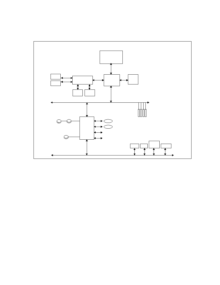
1.0 FUNCTIONAL OVERVIEW
The SLC90E66 is a high integration, multifunction PCI device which is used in combination with an appropriate
Northbridge memory controller to provide a significant portion of the overall system level functionality
FIGURE 1 shows a system configuration using the SLC90E66.
FIGURE 1 - SYSTEM BLOCK DIAGRAM OF PC SYSTEM USING SLC90E66
PCI-to-ISA/EIO Bridge
The SLC90E66 is compatible with the PCI 2.1 specification, as well as the ISA bus specification. The SLC90E66
operates as a PCI master for internal modules, such as the IDE controller, USB controller, DMA controller, distributed
DMA masters, and on behalf of ISA masters. The SLC90E66 operates as a slave for its internal registers and for
cycles that are passed to the ISA or EIO buses. The SLC90E66 positively decodes all internal registers.
The SLC90E66 can be configured for a full ISA bus or a subset of the ISA bus called the Extended IO (EIO) bus.
When configured as an EIO bus, unused signals can be configured for use as general purpose inputs and outputs
(GPIO). Like standard ISA bridge devices, the SLC90E66 also provides byte-swap logic, I/O recovery support, wait-
state generation, and SYSCLK generation. Chip select signals are also generated for external devices: keyboard
controller, BIOS, external RTC, external microcontroller, and two programmable chip selects. The SLC90E66 is
designed to directly drive up to 5 ISA slots without the need for external data or address buffering.
The SLC90E66 can be configured as either a subtractive decode PCI to ISA bridge or as positive decode bridge. This
allows a system designer to place another subtractive decode bridge in the system, such as a PCI docking device.
Ultra ATA/66 PCI IDE Controller
The SLC90E66 Ultra ATA/66 IDE controller implements two IDE channels supporting up to four IDE devices such as
IDE hard disks and CD-ROM drives. Each IDE device can have independent timings. IDE transfer rates up to 14
Mbytes/second in PIO mode or 66 Mbytes/second in bus master mode are supported. A 32x32-bit buffer is
Pentiium II
or
Pentium III
Processor
Graphics
Accelerator
Intel
FW82443BX
North Bridge
Main
Memory
(SDRAM)
PCI Bus (3.3V or 5V)
PCI Slots
Victory66
SLC90E66
South Bridge
GP[I,O](30+)
SMBus
USB 2
USB 1
Hard
Disk
CD ROM
Hard
Disk
Ultra ATA/66
IDE Interface
ISA/EIO Bus
(3.3; 5V Tolerant)
Audio
KBD
SMSC
Super I/O
BIOS
2x AGP
Frame
Buffer
Video
BIOS
Display
TV

SMSC DS SLC90E66
Page 14
Rev. 07/10/2002
implemented for each channel so that both channels can operate concurrently and achieve optimal transfers. No ISA
DMA resources are consumed.
Signicant flexibility in system design and power management is provided. The two IDE signal channels are
electrically isolated supporting the implementation of a glueless swap bay. They can be configured to the standard
primary and secondary channel (four devices) or primary drive 0 and primary drive 1 (two devices).
Enhanced Universal Serial Bus (USB) Controller
The SLC90E66 provides Open Host Controller Interface (OHCI) USB support. This includes support that allows
legacy software to use a USB-based keyboard and mouse. The SLC90E66 USB controller has been enhanced to
support wake-up from Power-on suspend (POS).
Compatibility Modules (DMA Controller, Timer/Counter, and Interrupt Controller)
The DMA controller provides seven independently programmable channels through the functionality of two 8237 DMA
controllers. Channels [0-3] are hardwired to 8-bit, count-by-byte transfers, and channels [5-7] are hardwired to 16-bit,
count-by-word transfers. Each of the seven DMA channels can be programmed to support fast Type-F transfers.
The DMA controller supports two different methods for handling legacy DMA via the PCI bus. The Distributed DMA
method allows reads and writes to 8237 registers to be distributed to other PCI slave devices. The serial interrupt
scheme typically associated with Distributed DMA is also supported.The PC/PCI protocol allows PCI-based
peripherals to initiate DMA cycles by encoding requests and grants through three PC/PCI nREQ/nGNT pairs. The two
methods can be used concurrently.
The integrated 82C54 controller provides three counters that provide the system timer, refresh request, and speaker
tone functions. A 14.31818 MHz oscillator input provides the clock source for these three counters.
The SLC90E66 interrupt controller is comprised of two 8259 interrupt controllers. The two interrupt controllers are
cascaded so that 14 external and two internal interrupts are possible. The SLC90E66 also supports a serial interrupt
scheme. An external I/O APIC device is supported.
All registers in the Compatibility Block can be read and restored supporting complete system state save and restore
operations for suspend and advanced power management operation.
RTC
The SLC90E66 contains a Motorola MC146818A-compatible real-time clock (RTC) with 256 bytes of battery backed
RAM. The RTC keeps track of time of day and stores system information. An external 3V lithium battery maintains
the RTC functionality even when the system power is off. The RTC operates on a 32.768 Khz crystal.
The RTC also supports two lockable memory ranges. By setting bits in the configuration space, two 8-byte ranges
can be locked to read and write accesses preventing unauthorized reading of passwords or other system security
information.
The RTC also supports a date alarm, allowing for scheduling a wake up event up to 30 days in advance, rather than
just 24 hours in advance.
GPIO and Chip Selects
The SLC90E66 provides various general purpose inputs and outputs (GPIO) for custom system design. The number
of inputs and outputs varies depending on the configuration. The SLC90E66 also provides two programmable chip
selects which allow designer to place devices on the X-Bus without the need for external decoding logic.
Enhanced Power Management
The SLC90E66 power management functions include enhanced clock control, local and device monitoring of up to 14
devices, and various low-power (suspend) states, such as Power-On Suspend, Suspend-to-RAM, and Suspend-to-
Disk. A hardware-based thermal management circuit allows software-independent entrance to low-power states.
Various external events, such as notebook lid open/close, modem/phone ring, suspend/resume button, battery low
warning signals can be connected to dedicated pins of the SLC90E66. The SLC90E66 provides full support for the
Advanced Configuration and Power Interface (ACPI) Specification.

SMSC DS SLC90E66
Page 15
Rev. 07/10/2002
System Management Bus (SMBus)
The SLC90E66 integrates a SMBus Host controller, which includes a Host interface for the CPU to communicate with
SMBus slaves and a Slave interface that allows external masters to activate power management events.
Configurability
PIIX/66 provides a wide range of system configuration options, includeing full 16-bit I/O decode on internal modules,
dynamic disable on all the internal modules, various peripheral decode options, and many other system configuration
options.

SMSC DS SLC90E66
Page 16
Rev. 07/10/2002
2.0 SIGNAL DESCRIPTION
This section provides a detailed description of each SLC90E66 signal. The signals are arranged in functional groups
according to their associated function.
The `n' symbol at the beginning of a signal name indicates an active low signal such that the active, or asserted state
occurs when the signal is at a low voltage level. When `n' is not present before the signal name, it indicates that the
signal is an active high signal such that the signal is asserted when at the high voltage level.
The term assert or assertion indicates that a signal is active, independent of whether that level is represented by a
high or low voltage. The term negate or negation indicates that a signal is inactive, independent of whether that level
is represented by a high or low voltage.
Certain signals have different functions, depending on the configuration programmed in the PCI configuration space.
This signal whose function is being described is in bold font. Default configurations for GPIO signals are shown in
Table 1 and Table 2.
The signal state during reset, after reset, and during power-on suspend (POS) is shouwn for all output signals.
During Reset refers to when the PCIRST# signal is asserted. After Reset is immediately after negation of PCIRST#
and the signal may change value anytime thereafter.
The term High-Z means tri-stated. The term Undefined means the signal could be high, low, tri-stated, or in some in-
between level.
Some of the power management signals are reset with the nRSMRST input signal. The functionality of these signals
during nRSMRST assertion is described in section 11.3 Suspend/Resume Control Mechanism.
The following notations are used to describe the I/O buffer type.
Buffer type
Description
I
Input only signal.
O
Totem pole output is a standard active driver.
I/O
Bi-Directional Input/Output, tri-state input/output pin.
OD
Open drain.
I/OD
Input/Open Drain Output is a standard input buffer with an Open Drain Output.
s/t/s
Sustained tri-state, is an active low tri-state signal owned and driven by one and only one
agent at a time. The agent that drives a s/t/s pin low must drive it high for at least one
clock before allowing it to float. A new agent can not start driving a s/t/s signal any sooner
than one clock after the previous owner tri-states it. An external pull-up resistor is
required to sustain the inactive state until another agent drives it and must be provided by
the central resource.
V
Power supply pin.
All 3V output signals can drive 5V TTL inputs. Most of the 3V input signals are 5V tolerant (See Table 3 for
identification of signals which are not 5V tolerant). The 3V input signals which are powered via the RTC or Suspend
power planes should not exceed their power supply voltage (see section 2.2 Power Planes for information). The
open drain (OD) CPU interface signals should be pulled up to the CPU interface signal voltage.

SMSC DS SLC90E66
Page 17
Rev. 07/10/2002
2.1 Signals
2.1.1
PCI BUS INTERFACE
NAME
TYPE
DESCRIPTION
AD[31-0]
I/O
PCI ADDRESS/DATA. AD[31:0] is the multiplexed PCI address and data bus. During
address phases, AD[31:0] is driven with a 32-bit physical byte address. AD[31:0] drives or
receives data during the data phases.
A Bus transaction consists of an address phase followed by one or more data phases.
Little-endian byte ordering is used. AD[7:0] define the least significant byte (LSB) and
AD[31:24] the most significant byte (MSB).
When the SLC90E66 is a Target, AD[31:0] are inputs during the address phase of a
transaction. During the following data phase(s), the SLC90E66 may be asked to supply
data on AD[31:0] for a PCI read, or accept data for a PCI write.
As an Initiator, the SLC90E66 drives a valid address on AD[31:2] and 0 on AD[1:0] during
the address phase, and drives write or latches read data on AD[31:0] during the data
phase.
During Reset: High-Z After Reset: High-Z During POS: High-Z
C/nBE[3-0]
I/O
BUS COMMAND (C) and BYTE ENABLE (BE). The Command and Byte Enable signals
are multiplexed on the same pins. During the address phase of a bus transaction, the
C/nBE[3-0] signals define the bus command. During the data phase of a bus transaction,
the C/nBE[3-0] signals are byte enables that determine which byte lanes carry requested
data. C/nBE0 applies to byte 0, C/nBE1 applies to byte 1, etc. The SLC90E66 drives
C/nBE[3-0] as an initiator and monitors C/nBE[3-0] as a target.
During Reset: High-Z After Reset: High-Z During POS: High-Z
nFRAME
I/O
CYCLE FRAME. nFRAME is asserted by the PCI initiator to indicate the start and
duration of a PCI transfer. NFRAME is negated during the final assertion. nFRAME is an
input when the SLC90E66 is a target. nFRAME is an output when the SLC90E66 is an
initiator. nFRAME remains tri-stated until driven by the SLC90E66 as an initiator.
During Reset: High-Z After Reset: High-Z During POS: High-Z
nDEVSEL
I/O
DEVICE SELECT. The SLC90E66 asserts nDEVSEL to claim a PCI transaction through
positive decoding or subtractive decoding (if enabled).
As an output, the SLC90E66 asserts nDEVSEL when it samples IDSEL active in
configuration cycles to SLC90E66 configuration registers. The SLC90E66 also asserts
nDEVSEL when an internal SLC90E66 address is decoded or when the SLC90E66
subtractively or positively decodes a cycle for the ISA/EIO bus or IDE device.
As an input, nDEVSEL indicates the response to a SLC90E66 initiated transaction and is
also sampled when deciding whether to subtractively decode the cycle.
nDEVSEL is asserted or sampled at medium decode time. nDEVSEL is tri-stated from the
leading edge of nPCIRST. It remains tri-stated until driven by the SLC90E66 as a target.
During Reset: High-Z After Reset: High-Z During POS: High-Z

SMSC DS SLC90E66
Page 18
Rev. 07/10/2002
NAME
TYPE
DESCRIPTION
nIRDY
I/O
INITIATOR READY. nIRDY, in conjunction with nTRDY, indicates the ability of the
SLC90E66, as an Initiator, to complete the current data phase of the transaction. A data
phase is completed on any clock both nIRDY and nTRDY are sampled asserted. During a
write, nIRDY indicates the SLC90E66 has valid data present on AD[31-0]. During a read,
it indicates the SLC90E66 is prepared to latch data.
nIRDY is an input to the SLC90E66 when the SLC90E66 is the target and an output
when the SLC90E66 is an initiator. It remains tri-stated until driven by the SLC90E66 as a
master.
During Reset: High-Z After Reset: High-Z During POS: High-Z
nTRDY
I/O
TARGET READY. nTRDY, in conjunction with nIRDY, indicates the ability of the
SLC90E66 to complete the current data phase of the PCI transaction. A data phase is
completed on any clock both nIRDY and nTRDY are sampled asserted. During a read,
nTRDY indicates that the SLC90E66, as a Target, has placed valid data on AD[31-0].
During a write, it indicates the SLC90E66, as a Target is prepared to latch data.
nTRDY is an input to the SLC90E66 when the SLC90E66 is the initiator and an output
when the SLC90E66 is a target. It remains tri-stated until driven by the SLC90E66 as a
target.
nTRDY is tri-stated from the leading edge of nPCIRST. nTRDY remains tri-stated until
driven by the SLC90E66 as a slave.
During Reset: High-Z After Reset: High-Z During POS: High-Z
nSTOP
I/O
STOP. nSTOP indicates that the SLC90E66, as a Target, is requesting the initiator to stop
the current transaction. As an initiator, nSTOP causes the SLC90E66 to stop the current
transaction.
nSTOP is an output when the SLC90E66 is a Target and an input when the SLC90E66 is
an initiator. nSTOP is tri-stated from the leading edge of nPCIRST, and it remains tri-
stated until driven by the SLC90E66 as a slave.
During Reset: High-Z After Reset: High-Z During POS: High-Z
IDSEL
I
INITIALIZATION DEVICE SELECT. IDSEL is used as a chip select during PCI
configuration read and write cycles. The SLC90E66 samples IDSEL during the address
phase of a transaction. The SLC90E66 responds by asserting nDEVSEL on the next
cycle if IDSEL is sampled active during configuration read or write cycles.
nPHOLD
O
PCI HOLD. The SLC90E66 asserts nPHLD to indicate its desire to use the PCI bus.
nPHLD has the highest priority among the five bus request signals. Once the request is
granted, nPHLDA will remain asserted by the PCI arbiter until the nPHLD is de-asserted
by the SLC90E66. The SLC90E66 implements the passive release mechanism by
toggling nPHOLD inactive for one PCICLK.
During Reset: High-Z After Reset: High During POS: High
nPHLDA
I
PCI HOLD ACKNOWLEDGE. Assertion of nPHLDA by the PCI arbiter indicates that the
SLC90E66 has been granted use of the PCI bus. Once it is asserted, nPHLDA cannot be
de-asserted until nPHLD is de-asserted first.
nSERR
I/O
SYSTEM ERROR. nSERR can be driven active by any PCI device that detects a system
error condition. Upon sampling nSERR active, the SLC90E66 can be programmed to
generate a non-maskable interrupt (NMI) to the CPU.
During Reset: High-Z After Reset: High-Z During POS: High-Z

SMSC DS SLC90E66
Page 19
Rev. 07/10/2002
NAME
TYPE
DESCRIPTION
PAR
I/O
CALCULATED PARITY SIGNAL. PAR is "even" parity and is calculated on 36 bits
(AD[31-0] and C/nBE[3-0]). Even parity is such that the number of `1s' in the 37 bits
inclusive of PAR is always even. PAR is calculated on 36 bits regardless of the valid byte
enables. PAR is generated during address and data phases and is only guaranteed to be
valid for the PCI clock following the corresponding data or address phase. PAR is driven
and tri-stated identically to the AD[31-0] lines except that PAR is delayed by exactly one
PCI clock.
PAR is an output during the address phase (delayed by one clock) for all SLC90E66
initiated transactions. It is also an output during the data phase (delayed by one clock)
when the SLC90E66 is the initiator of a PCI write transaction and when it is the target of a
read transaction.
During Reset: High-Z After Reset: High-Z During POS: High-Z
nCLKRUN
I/O
3.3V/5V
CLOCK RUN. SLC90E66 uses this signal to communicate to PCI peripherals that the PCI
clock will be stopped. Peripherals can assert nCLKRUN to request that the PCI clock be
restarted or to keep it from stopping. nCLKRUN follows the protocol specified in the PCI
Mobile Design Guide Revision 1.0.
During Reset: Low After Reset: Low During POS: High
nPCIRST
O
Reset. The SLC90E66 asserts nPCIRST to reset devices that resides on the PCI bus.
The SLC90E66 asserts nPCIRST during power-up and when a hard reset sequences is
initiated through the RC register. nPCIRST is asserted for a minimum of 1 ms after
PWROK is driven active. It is driven for a minimum of 1ms when initiated through the RC
register. The signal is driven asynchronously relative to PCICLK.
During Reset: Low. After Reset: High. During POS: High.
2.1.2
ISA/EIO INTERFACE SIGNALS
NAME
TYPE
DESCRIPTION
SA[19-0]
I/O
SYSTEM ADDRESS[19-0]. These bi-directional signals define the address with a
granularity of one byte within the one megabyte address space defined by LA[23-
17]. The address lines SA[19-17] that are coincident with LA[19-17] are defined to have
the same values as LA[19-17] for all memory cycles. For I/O accesses, only SA[15-0] are
used, and SA[19-16] are undefined. SA[19-0] are outputs when the SLC90E66 owns the
ISA bus. They are inputs when an external ISA master owns the ISA bus.
During Reset: High-Z After Reset: Undefined During POS: Last SA
LA[23-17]/
GPO[7-1]
I/O
ISA LA[23-17]. The LA[23-17] address lines allow accesses to physical memory on the
ISA bus up to 16 Mbytes. They are outputs when the SLC90E66 owns the ISA bus. They
become inputs whenever an ISA master owns the ISA bus. These signals are at an
undefined state upon nPCIRST.
GPO. If EIO configuration is selected, these signals become general purpose outputs.
During Reset: High-Z After Reset: Undefined. During POS: Last LA/GPO
SD[15-0]
I/O
SYSTEM DATA. SD[15-0] provide the 16-bit data path for devices residing on the ISA
bus. SD[15-8] are the high order byte and SD[7-0] are the low order byte. SD[15-0] are
undefined during refresh.
During Reset: High-Z After Reset: Undefined. During POS: High-Z.
nSMEMR
O
STANDARD MEMORY READ. The SLC90E66 asserts nSMEMR to request an ISA
memory slave to drive data onto the data lines. If the memory access is below the
1Mbyte range (00000000h-000FFFFFh) during DMA, SLC90E66 master, or ISA master
cycles, the SLC90E66 asserts nSMEMR. nSMEMR is a delayed version of nMEMR.
During Reset: High-Z After Reset: High During POS: High

SMSC DS SLC90E66
Page 20
Rev. 07/10/2002
NAME
TYPE
DESCRIPTION
nSMEMW
O
STANDARD MEMORY WRITE. The SLC90E66 asserts nSMEMW to request an ISA
memory slave to receive data from the data lines. If the memory access is below the
1Mbyte range (00000000h-000FFFFFh) during DMA, SLC90E66 master, or ISA master
cycles, the SLC90E66 asserts nSMEMW. nSMEMW is a delayed version of nMEMW.
During Reset: High-Z After Reset: High During POS: High
nMEMR
I/O
MEMORY READ. nMEMR is the command to a memory slave that it may drive data
onto the ISA data bus. nMEMR is an output when the SLC90E66 owns the ISA bus or
during refresh cycles. nMEMR is an input when an ISA master other than the SLC90E66
owns the ISA bus. For DMA cycles, the SLC90E66, as a master, asserts nMEMR.
During Reset: High-Z After Reset: High During POS: High.
nMEMW
I/O
MEMORY WRITE. nMEMW is the command to a memory slave that it may latch data
from the ISA data bus. nMEMW is an output when the SLC90E66 owns the ISA bus.
nMEMW is an input when an ISA master other than the SLC90E66 owns the ISA bus.
For DMA cycles, the SLC90E66, as a master, asserts nMEMW.
During Reset: High-Z After Reset: High During POS: High.
nREFRESH
I/O
REFRESH. As an output, nREFRESH is used to indicate when a refresh is in progress.
The SA[7-0] should be applied to the row address of all banks of DRAM on the ISA bus
so that when nMEMR is asserted, the entire expansion bus DRAM is refreshed. Memory
slaves must not drive data onto the bus during refresh cycles. This signal is an output
only when the SLC90E66 DMA controller is a master on the bus responding to the
internally generated request for refresh.
As an input signal, nREFRESH is driven by 16-bit ISA masters to initiate refresh cycles.
During Reset: High-Z After Reset: High During POS: High
AEN
O
ADDRESS ENABLE. AEN is asserted during DMA cycles to prevent I/O slaves from
claiming DMA cycles as valid I/O cycles. When negated, it indicates that an I/O slave
may respond to address and I/O commands. When asserted, it informs I/O resources on
the ISA bus that a DMA transfer is occurring on the ISA bus.
The signal is driven high during SLC90E66 initiated refresh cycles. It is driven low upon
nPCIRST.
During Reset: High-Z After Reset: Low During POS: Low
BALE
O
BUS ADDRESS LATCH ENABLE. BALE is asserted by the SLC90E66 to indicate that
the address (SA[19-0] and LA [23-17]) and nSBHE signal lines are valid. The LA[23-17]
are latched on the trailing edge of BALE. BALE remains asserted throughout DMA and
ISA master cycles.
During Reset: High-Z After Reset: Low During POS: Low
nSBHE
I/O
SYSTEM BYTE HIGH ENABLE. When asserted indicates that a byte is being
transferred on the upper byte (SD[15-8]) of the data bus. It is negated during refresh
cycles. nSBHE is an output when the SLC90E66 owns the ISA Bus. It becomes an input
when an external ISA master owns the ISA Bus.
During Reset: High-Z After Rest: Undefined During POS: High
nIOCHK/
GPI0
I
I/O CHANNEL CHECK. When asserted, the signal indicates that a parity or an
uncorrectable error has occurred for a device or memory on the ISA Bus. A NMI will be
generated to the CPU if the NMI feature is enabled.
GPI[0]. If the EIO bus is configured, this signal becomes a general purpose input.

SMSC DS SLC90E66
Page 21
Rev. 07/10/2002
NAME
TYPE
DESCRIPTION
IOCHRDY
I/O
I/O CHANNEL READY. When asserted, the signal indicates that wait states are
required to complete the cycle. This signal is normally high. IOCHRDY is an input when
the SLC90E66 owns the ISA Bus and the CPU or a PCI agent is accessing an ISA slave,
or during DMA transfers. It becomes an output when an external ISA master owns the
ISA Bus and is accessing DRAM or a SLC90E66 register. As an output, the signal is
driven low (negated) from the falling edge of the ISA commands by the SLC90E66. After
data is available for an ISA master read or the SLC90E66 latches the data for a write
cycle, IOCHRDY is asserted for 70ns. After 70 ns, IOCHRDY is floated. The 70 ns
includes both the drive time and the time it takes the SLC90E66 to float IOCHRDY. The
SLC90E66 does not drive the signal when it is not the target of a bus master cycle.
During Reset: High-Z After Reset: High-Z During POS: High-Z
nIOCS16
I
16-BIT I/O CHIP SELECT. This signal is driven by ISA resources to indicate that the ISA
I/O device supports 16-bit I/O bus cycles.
nIOR
I/O
I/O READ. nIOR is the command to an ISA I/O device to indicate that the slave may
drive data on SD[15-0]. The I/O device must hold the data valid until after nIOR is
negated. nIOR is an output when the SLC90E66 owns the ISA Bus. nIOR is an input
when an external ISA master owns the ISA Bus.
During Reset: High-Z After Reset: High During POS: High
nIOW
I/O
IO/ WRITE. nIOW is the command to an ISA I/O device indicating that the I/O device
may latch data from the ISA data bus (SD[15-0]). nIOW is an output when the
SLC90E66 owns the ISA Bus. nIOW is an input when an external ISA master owns the
ISA bus.
During Reset: High-Z After Reset: High During POS: High
nMEMCS16
I/O
MEMORY CHIP SELECT 16. nMEMCS16 is a decode of LA[23-17] without any
qualification of the command signals. ISA devices that are 16-bit memory devices assert
this signal. The SLC90E66 ignores nMEMCS16 during I/O and refresh cycles. It is used
by byte-swap logic during DMA cycles. This signal is an input when the SLC90E66
owns the ISA Bus. This signal is an output when an ISA master owns the ISA Bus. The
SLC90E66 drives this signal low during ISA master to PCI memory cycles.
During Reset: High-Z After Reset: High-Z During POS: High-Z
nZEROWS
I
ZERO WAIT STATES. The signal is asserted by an ISA slave after the address and
command signals are decoded to indicate that the current cycle can be shortened. A 16-
Bit ISA memory cycle can be reduced to two SYSCLKs. An 8-Bit memory or I/O cycle
can be reduced to three SYSCLKs. nZEROWS has no effect on 16-Bit I/O cycles.
If IOCHRDY is negated and nZEROWS is asserted during the same clock, then
nZEROWS is ignored and wait states are added while IOCHRDY is negated.
RSTDRV
O
RESET DRIVE. The SLC90E66 asserts RSTDRV to reset devices that reside on the
ISA/EIO bus. The SLC90E66 asserts the signal during hard reset and during power-up.
RSTDRV is asserted during power-up and negated after PWROK is driven active. It is
also driven active for a minimum of 1ms if a hard reset has been programmed in the RC
register.
During Reset: High After Reset: Low During POS: Low

SMSC DS SLC90E66
Page 22
Rev. 07/10/2002
2.1.3
XBUS INTERFACE SIGNALS
NAME
TYPE
DESCRIPTION
A20GATE
I
ADDRESS 20 GATE. This input from the keyboard controller is internally "ORed" with bit
1 (FAST_A20) of the Port 92 register, which is then output via the nA20M signal.
nBIOSCS
O
BIOS CHIP SELECT. This signal is asserted during read or write accesses to the
enabled BIOS memory range by decoding the SA[19-0] and LA[23-17] address signals.
During DMA cycles, nBIOSCS is not generated.
During Reset: High After Reset: High During POS: High
nKBCCS/
GPO26
O
KEYBOARD CONTROLLER CHIP SELECT. This signal is asserted during I/O Read or
Write accesses to Keyboard Controller I/O ports 60h and 64h by decoding the ISA
addresses SA[19-0] and LA[23-17].
GPO26. If the keyboard controller does not require a fully decoded chip select signal, this
pin can be used as a general purpose output.
During Reset: High After Reset: High During POS: High.
nMCCS
O
MICROCONTROLLER CHIP SELECT. nMCCS is asserted during I/O read or write
accesses to I/O locations 62h and 66h by decoding the ISA addresses SA[19-0] and
LA[23-17].
During Reset: High After Reset: High During POS: High
RTCALE/
GPO25
O
REAL TIME CLOCK ADDRESS LATCH ENABLE. RTCALE is used to latch the memory
address into an external RTC when the internal RTC is disabled or when the internal RTC
is relocated (see RTC Functional Description). A write to port 70h with the appropriate
RTC memory address causes RTCALE to be asserted. RTCALE is asserted on the falling
edge of nIOW and remains asserted for two SYSCLKs. RTCALE is not generated when
the internal RTC is enabled and is at the default location as programmed in the PCI
configuration registers.
GPO25. This pin can be used as GPO25 when the internal RTC is enabled.
During Reset: Low After Reset: Low During POS: Low/GPO
nRTCCS/
GPO24
O
RTC CHIP SELECT. nRTCCS is asserted during Read or Write I/O accesses to I/O
location 71h RTC when the internal RTC is disabled or when the internal RTC is relocated
(see RTC Functional Description). nRTCCS is not generated when the internal RTC is
enabled and is at the default location as programmed in the PCI configuration registers.
nRTCCS can be tied to a pair of external OR gates to generate the real time clock read
and write command signals.
GPO24. This pin can be used as GPO24 when the internal RTC is enabled.
During Reset: High After Reset: High During POS: High / GPO
nPCS[1-0]
O
PROGRAMMABLE CHIP SELECTS. These active low chip select signals are asserted
for ISA I/O cycles which are generated by PCI masters and which hit the programmable
I/O ranges defined in the power management section. The X-Bus buffer signals (nXOE
and nXDIR) are enabled while the chip select is asserted.
During Reset: High After Reset: High During POS: High
nRCIN
I
RESET CPU. This signal from the keyboard controller is used to generate an INIT signal
to the CPU.

SMSC DS SLC90E66
Page 23
Rev. 07/10/2002
NAME
TYPE
DESCRIPTION
nXOE/
GPO23
O
XBus Transceiver Output Enable. nXOE is tied to the output enable of a 245
transceiver that buffers the XD[7-0] from SD[7-0]. nXOE is asserted anytime a X-Bus
device is decoded, and the device's decode is enabled in the X-Bus Chip Select Enable
Register (nBIOSCS, nKBCCS, nRTCCS, and nMCCS) or the Device Resource B and C
(nPCS0 and nPCS1). nXOE is asserted from the falling edge of the ISA commands for
PCI Master and ISA master initiated cycles. It is negated from the rising edge of the ISA
command signals for PCI Master initiated cycles and SA[16-0] and LA[23-17] address for
ISA Master initiated cycles.
Note: In some cases, nXOE is also generated during access to an Xbus peripheral in
which its decode space has been disabled and during access to relocated RTC registers.
GPO23. If the X-Bus is not used, this signal can be used as a general purpose output.
During Reset: High After Reset: High During POS: High/GPO
nXDIR/
GPO22
O
XBUS TRANSCEIVER DIRECTION. nXDIR is tied directly to the direction control of a
245 transceiver that buffers XD[7-0] from SD[7-0]. nXDIR is asserted (low) for all I/O read
cycles. nXDIR is only asserted for memory cycles if the BIOS or APIC space has been
decoded. For PCI and ISA master initiated read cycles, nXDIR is asserted from the falling
edge of either nIOR or nMEMR (from nMEMR only if BIOS or APIC space has been
decoded), depending on the cycle type. PCI and ISA master initiated read cycles. When
the rising edge of nIOR or nMEMR occurs, the SLC90E66 negates nXDIR. For DMA read
cycles from the X-Bus, XDIR is driven low from nDACKx falling and negated from
nDACKx rising. At all other times, nXDIR is negated high.
GPO22. If the X-Bus not used, then this signal can be programmed to be a general
purpose output.
During Reset: High After Reset: High During POS: High/GPO
2.1.4 DMA
SIGNALS
NAME
TYPE
DESCRIPTION
DREQ[0-3]
DREQ[5-7]
I
DMA REQUEST. The DREQ lines are used to request DMA services from the DMA
controller or for a 16-bit ISA master to gain control of the ISA bus. The active level (high
or low) can be programmed via the DMA Command Register. All inactive to active edges
of DREQ are assumed to be asynchronous. The request must remain active until the
corresponding nDACK is asserted.
nDACK[0-3]
nDACK[5-7]
O
DMA Acknowledge. Each nDACK signal corresponds to the respective DREQ
signal. The nDACK output lines indicate that a request for DMA service has been
granted by the SLC90E66 or that a 16-bit master has been granted the bus. The active
level (high or low) is programmed via the DMA Command Register. These lines should
be used to decode the DMA slave device with the IOR# or IOW# line to indicate
selection. If used to signal acceptance of a bus master request, this signal indicates
when it is legal to assert nMASTER. If the DREQ goes inactive before nDACK being
asserted, the nDACK signal will not be asserted.
During Reset: High After Reset: High During POS: High
nREQ[A-C]/
GPI[2-4]
I
PC/PCI DMA REQUEST. These are DMA requests for the PC/PCI protocol. They are
used by a PCI agent to request DMA services and follow the PCI Expansion Channel
Passing protocol as defined in the PCI DMA section.
GPI[2-4]. If the PC/PCI protocol is not used, these can be used as general purpose
inputs.

SMSC DS SLC90E66
Page 24
Rev. 07/10/2002
NAME
TYPE
DESCRIPTION
nGNT[A-C]/
GPO[9-11]
O
PC/PCI DMA GRANT. These signals are the DMA grants for the PC/PCI protocol. They
are used by the SLC90E66 to acknowledge DMA services and follow the PCI Expansion
Channel Passing protocol as defined in the PCI DMA section.
GPO[9-11]. If the PC/PCI protocol is not used, these can be used as general purpose
outputs..
During Reset: High After Reset: High During POS: High/GPO
TC
O
TERMINAL COUNT. The SLC90E66 asserts TC to DMA slaves after a new address has
been output and the byte count expires with that transfer. TC remains asserted until AEN
is negated, unless AEN is negated during an autoinitialization. TC is negated before
AEN is negated during an autoinitialization.
During Reset: Low After Reset: Low During POS: Low
2.1.5
INTERRUPT CONTROLLER AND APIC SIGNALS
NAME
TYPE
DESCRIPTION
IRQ0/
GPO14
O
INTERRUPT REQUEST 0. If the external APIC is used, this is an output reflecting the
state of the internal IRQ0 signal from the system timer.
GPO[14]: General purpose output if there is no external APIC.
During Reset: Low After Reset: Low During POS: IRQ0/GPO
IRQ1
I
INTERRUPT REQUEST 1. A low to high edge transition on IRQ1 is latched by
SLC90E66. IRQ1 must remain asserted until after the interrupt is acknowledged. If IRQ1
goes is negated before it is acknowledged, a default IRQ7 is reported in response to the
interrupt acknowledge cycle. IRQ1 cannot be programmed to be level sensitive.
IRQ[3-7, 9 -
11, 14-15]
I
INTERRUPT REQUESTS 2-3, 9-11, 14-15. These interrupts may be programmed for
either an edge sensitive or a high level sensitive mode. The default is edge sensitive
mode. If the request goes inactive before it is acknowledged, a default IRQ7 is reported
in response to the interrupt acknowledge cycle.
nIRQ8/
GPI6
I/O
INTERRUPT REQUEST 8. nIRQ8 is an active low edge triggered interrupt input from an
external RTC.
GPI6. If the internal RTC is used, this pin can be used a general purpose input.
If an APIC is enabled, this pin becomes an output and must not be programmed as a
general purpose input..
IRQ12/M
I
INTERRUPT REQUEST 12. This is an interrupt request channel 12 which may be
programmed for either an edge sensitive or a high level sensitive mode. The default is
edge sensitive mode. If the request goes inactive before it is acknowledged, a default
IRQ7 is reported in response to the interrupt acknowledge cycle.
Additionally, this pin can also be programmed to provide the mouse interrupt function.
When the mouse interrupt is selected, the SLC90E66 latches a low to high transition on
this signal and generates an INTR to the CPU as IRQ12. An internal IRQ12 interrupt will
continue to be generated until a Reset or an I/O read access to address 60h is detected.
nPIRQ[A-D]
I/OD
PCI
PROGRAMMABLE INTERRUPT REQUEST. The nPIRQx signals are active low, level
sensitive interrupt inputs. They can be individually steered to ISA interrupts IRQ[3-7,9-
12,14-15]. The USB controller uses nPIRQD as its interrupt output signal. The Power
Management controller uses nPIRQA as its interrupt output.

SMSC DS SLC90E66
Page 25
Rev. 07/10/2002
NAME
TYPE
DESCRIPTION
SERIRQ/
GPI7
I/O
SERIAL INTERRUPT REQUEST. Serial interrupt input decoder, typically used with the
Distributed DMA protocol.
GPI7. If not using DDMA serial interrupts, this pin can be used as a general-purpose
input.
IRQ9OUT/
GPO29
O
IRQ9OUT. IRQ9OUT is used to route the internally generated SCI and SMBus
interrupts out of the SLC90E66 for connection to an external IO-APIC.
GPO29. If APIC is disabled, this signal pin is a General Purpose Output.
During Reset: High After Reset: High During POS: IRQ9OUT/GPO
nAPICCS/
GPO13
O
APIC CHIP SELECT. This signal is asserted when the APIC Chip Select is enabled and
a PCI originated cycle is positively decoded within the programmable I/O APIC address
space.
GPO13. When the external APIC is not used, then this pin can be used as general
purpose output.
During Reset: High After Reset: High During POS: High/GPO
nAPICREQ/
GPI5
I
APIC REQUEST. The external APIC device asserts this signal prior to sending an
interrupt over the APIC serial bus. When the SLC90E66 samples the active signal, it will
assert the nAPICACK after the internal buffers (Type-F DMA buffer) are flushed. Once
the buffers are flushed, SLC90E66 asserts nAPICACK which indicates to the external
APIC that it can proceed to send the APIC interrupt. The nAPICREQ input must be
synchronous to PCICLK.
GPI5. If no external APIC is used, then this pin can be used as general purpose input.
nAPICACK/
GPO12
O
APIC ACKNOWLEDGE. The SLC90E66 asserts this signal after its internal buffers are
flushed in response to the nAPICREQ signal. The asserted nAPICACK signal indicates
that the APIC can proceed to send the APIC interrupt. This signal is synchronous to
PCICLK.
GPO12. If no external APIC is used, then this pin can be used as general purpose
output.
2.1.6 CPU
INTERFACE
SIGNALS
NAME
TYPE
DESCRIPTION
nA20M
OD
ADDRESS 20 MASK. The SLC90E66 asserts this signal to the CPU based on an
internal OR of bit 1 (FAST_A20), port 92 and the A20GATE input.
During Reset: High-Z After Reset: High-Z During POS: High-Z
nFERR
I
NUMERIC COPROCESSOR ERROR. This signal is connected to the coprocessor
error of the CPU and, when asserted by the CPU, the SLC90E66 generates an IRQ13
to the internal interrupt controller which then results in assertion of INT to the CPU. An
IO write to port F0h will cause the SLC90E66 to assert nIGNNE to the CPU while
nFERR is active. nFERR is used to gate the nIGNNE signal to ensure that nIGNNE is
not asserted to the CPU unless nFERR is active.
nIGNNE
OD
IGNORE NUMERIC EXCEPTION. This signal is output and is connected to the ignore
numeric exception pin of the CPU. NIGNNE is used only if the coprocessor error
reporting function is enabled in the SLC90E66. While nFERR is asserted, an IO write to
port F0h (Coprocessor Error Register) will cause nIGNNE to be asserted. It is negatedby
the SLC90E66 when nFERR is negated. If nFERR is not asserted when the port F0h is
written, the nIGNNE signal is not asserted.
During Reset: High-Z After Reset: High-Z During POS: High-Z

SMSC DS SLC90E66
Page 26
Rev. 07/10/2002
NAME
TYPE
DESCRIPTION
INTR
OD
CPU INTERRUPT. This is the interrupt request signal to the CPU to signal the CPU that
an interrupt request is pending and needs to be serviced. INTR is asynchronous with
respect to SYSCLK and PCICLK. INTR is an open-drain output signal, it requires a pull-
up resistor to the CPU voltage. The interrupt controller must be programmed following
nPCIRST to ensure that INTR is at a known state.
INTR may be latched or unlatched based on the CONFIG1 signal as follows: If
CONFIG1=0, INTR flows unlatched to the processor; If CONFIG1=1, INTR will be
latched when nSTPCLK is asserted and held for 5 PCICLK's after nSTPCLK is
deasserted.
During Reset: Low After Reset: Low During POS: Low
NMI
OD
NON-MASKABLE INTERRUPT. NMI is used to cause a non-maskable interrupt to the
CPU. The SLC90E66 asserts the NMI signal when either nSERR or nIOCHK is asserted
depending on the configuration defined in the NMI Status and Control Register. The
CPU detects a NMI when it detects a rising edge on NMI. After the NMI interrupt routine
processes the interrupt, the NMI status bits in the NMI Status and Control Register are
cleared by software. To determine the source of the interrupt, the handler must read this
register. The NMI is reset by setting the corresponding NMI source enable/disable bit in
the register. To enable NMI, the two NMI enable/disable bits in the register must be set
to 0, and the NMI mask bit in the NMI Enable/Disable and RTC Address Register must
be set to 0. Upon nPCIRST, this signal is driven low.
NMI may be latched or unlatched based on the CONFIG1 signal as follows: If
CONFIG1=0, NMI flows unlatched to the processor; If CONFIG1=1, NMI will be latched
when nSTPCLK is asserted and held for 5 PCICLK's after nSTPCLK is deasserted.
During Reset: Low After Reset: Low During POS: Low
nSLP
OD
SLEEP. This signal is the output to the Pentium II processor in order to put it into Sleep
state. For the Pentium processor, it is a No Connect.
During Reset: High-Z
After Reset: High-Z
During POS: High-Z
nSMI
OD
SYSTEM MANAGEMENT INPUT. nSMI is a synchronous output which is asserted in
response to one of many enabled hardware and software events. The CPU recognizes
the falling edge of SMI# as the highest priority interrupt in the system, with the exception
of INIT, CPURST, and FLUSH.
nSMI may be latched or unlatched based on the CONFIG1 signal as follows: If
CONFIG1=0, nSMI flows unlatched to the processor; If CONFIG1=1, nSMI will be
latched when nSTPCLK is asserted and held for 5 PCICLK's after nSTPCLK is
deasserted.
During Reset: High-Z After Reset: High-Z During POS: High-Z
nSTPCLK
OD
STOP CLOCK. nSTPCLK is an active low synchronous output that is asserted in
response to one of many enabled hardware and software events. NSTPCLK is
synchronous to PCICLK and is connected to the CPU.
During Reset: High-Z After Reset: High-Z During POS: High-Z
CPURST
OD
CPU RESET. The SLC90E66 asserts CPURST to reset the CPU during power up and
when a hard reset sequence is initiated through the RC register. CPURST is asserted a
minimum of 2 ms after PWROK is asserted or when initiated through the RC register.
The inactive edge of CPURST is driven synchronously to the rising edge of PCICLK. If a
hard reset is initiated through the RC register, the SLC90E66 resets its internal register
(in both core and suspend wells) to their default states.
Polarity is controlled by the CONFIG1 signal as follows: CONFIG1=0 (Pentium
processor) active high; CONFIG1=1 (Pentium II Processor) active low. For values During
Reset, After Reset, & During POS, refer to Section 11.3 Suspend/Resume Control
Mechanism"

SMSC DS SLC90E66
Page 27
Rev. 07/10/2002
NAME
TYPE
DESCRIPTION
INIT
OD
INITIALIZATION. The INIT signal is asserted in response to:
(1) PCI Shut Down special cycle is decoded.
(2) If nRCIN is asserted.
(3) A write occurs to port 92h, bit0.
(4) The System Reset bit in the Reset Control register is set to 0 and the Reset CPU
bit toggles from 0 to 1, triggering a soft reset.
When asserted, INIT remains asserted for approximately 64 PCI clocks before being
negated.
INIT may be latched or unlatched based on the CONFIG1 signal as follows: If
CONFIG1=0, INIT flows unlatched to the processor; If CONFIG1=1, INIT will be latched
when nSTPCLK is asserted and held for 5 PCICLK's after nSTPCLK is deasserted.
The polarity of this signal is determined by the CONFIG1 signal as follows: CONFIG1=0
(Pentium) active high; COnfig1=1 (Pentium II) active low.
The following conditions apply:
Pentium Processor:
During Reset: Low. After Reset: Low During POS: Low
Pentium II Processor:
During Reset: High
After Reset: High During POS: High
2.1.7 CLOCKS
NAME
TYPE
DESCRIPTION
PCICLK
I
FREE RUNNING PCI CLOCK. This clock runs at 30 or 33 MHz and provides timing for
all transactions on the PCI bus. All other PCI signals are sampled on the rising edge of
PCICLK, and all timing parameters are defined with respect to the edge. The signal must
be kept active, even if the PCI bus clock is not active, because other SLC90E66
functions operate on this clock..
OSC
I
14.31818 MHz CLOCK. This clock signal is used by the internal 8254 timer.
This clock signal may be stopped during suspend modes.
RTCX1,
RTCX2
IO
RTC CRYSTAL INPUTS. The 32.768 KHz clock source for the RTC is provided through
these pins. The XOSCSEL pin is used to configure these pins for an oscillator or for a
sigle ended clock.
When XOSCSEL = `0', these pins are configured for direct connection to a 32.768KHz
crystal. External capacitors are required.
When XOSCSEL = `1', The RTCX2 pin is configured for use with a single ended
32.768KHz clock source. This configuration allows the use of an external RTC without
requiring the use of two crystal oscillators. The clock output of the external RTC can be
used to drive the SLC90E66 internal RTC.
A 32.768KHz source (either crystal oscillator or single ended clock input) is required at
all times even if the internal RTC is not being used.
XOSCSEL
I
Crystal Oscilator Select. The XOSCSEL pin is used to cofigure the RTCX1 and RTCX2
pins for use with either a 32.768kHz input clock or a 32.768kHz crystal to drive the Real
Time Clock Interface.
When XOSCSEL = `0', the RTC uses a 32.768kHz crystal connected between the
RTCX1 and RTCX2 pins. When XOSCSEL = `1', the RTC is driven by a 32.768kHz
single-ended clock source connected to the XTAL2 pin.
CLK48
I
48 MHz CLOCK. This input receives a 48-MHz clock signal for the internal USB host
controller. This clock signal may be stopped during suspend modes.

SMSC DS SLC90E66
Page 28
Rev. 07/10/2002
NAME
TYPE
DESCRIPTION
SUSCLK
O
SUSPEND CLOCK. This is a 32.768KHz clock output is connected to the North Bridge
for maintenance of DRAM refresh during suspend modes. This signal is stopped during
Suspend-to-Disk mode and Soft Off mode.
During Reset: Running After Reset: Running During POS: Running
SYSCLK
O
ISA SYSTEM CLOCK. SYSCLK is the reference clock for the ISA bus. It drives the ISA
Bus directly. The SYSCLK is derived by dividing PCICLK by 4. The SYSCLK frequencies
supported are 7.5 MHz and 8.33 MHz.
During Reset: Running After Reset: Running During POS: Low
2.1.8 IDE
SIGNALS
NAME
TYPE
DESCRIPTION
PDD[15-0]
I/O
PRIMARY DISK DATA [15-0]. These signals are the data bus for transferring data to or
from the IDE device.
When the IDE controller is configured to support both primary and secondary channels,
these signals are connected to the primary IDE connector. When the IDE controller is
configured to support primary 0 and primary 1 devices, these signals are connected to
the primary 0 connector.
During Reset: High-Z After Reset: Undefined During POS: PDD
PDA[2-0]
O
PRIMARY DISK ADDRESS [2-0]. These signals select which byte, in either the ATA
command block or control block, is being accessed.
When the IDE controller is configured to support both primary and secondary channels,
these signals are connected to the primary IDE connector. When the IDE controller is
configured to support primary 0 and primary 1 devices, these signals are connected to
the primary 0 connector.
During Reset: High-Z After Reset: Undefined During POS: PDA
nPDCS1
O
PRIMARY DISK CHIP SELECT FOR 1F0h to 1F7h ADDRESS RANGE. Chip select
signal for ATA command register block.
When the IDE controller is configured to support both primary and secondary channels,
this signal is connected to the primary IDE connector. When the IDE controller is
configured to support primary 0 and primary 1 devices, this signal is connected to the
primary 0 connector.
During Reset: High After Reset: High During POS: High
nPDCS3
O
PRIMARY DISK CHIP SELECT FOR 3F6h. Chip select signal for the control register
block. Accesses to the other registers in the control block are forwarded to ISA by the
PCI-to-ISA bridge (Function 0) and nPDCS3 is not asserted.
When the IDE controller is configured to support both primary and secondary channels,
this signal is connected to the primary IDE connector. When the IDE controller is
configured to support primary 0 and primary 1 devices, this signal is connected to the
primary 0 connector.
During Reset: High After Reset: High During POS: High

SMSC DS SLC90E66
Page 29
Rev. 07/10/2002
NAME
TYPE
DESCRIPTION
nPDIOR
O
PRIMARY DISK IO READ. In normal IDE operation, this is the disk read command to
the IDE device indicating that it may drive data onto the PDD[15-0] lines. Data is latched
on the rising edge of nPDIOR. The IDE device is selected either by the ATA register file
chip selects (nPDCS1, nPDCS3) and the PDA[2:0] lines, or the IDE DMA slave
arbitration signals (nPDDACK).
In an Ultra ATA/66 read cycle, this signal is used as nDMARDY which is negated by the
SLC90E66 to pause Ultra ATA/66 transfers. In an Ultra ATA/66 write cycle, this signal is
used as the STROBE signal, with the drive latching data on rising and falling edges of
STROBE.
When the IDE controller is configured to support both primary and secondary channels,
this signal is connected to the primary IDE connector. When the IDE controller is
configured to support primary 0 and primary 1 devices, this signal is connected to the
primary 0 connector.
During Reset: High After Reset: High During POS: High
nPDIOW
O
PRIMARY DISK IO WRITE. In normal IDE operation, this is the disk Write command
to the IDE device indicating that it may latch data from the PD.[15-0] lines. Data is
latched by the IDE device on the rising edge of nPDIOW. The IDE device is selected
either by the ATA register file chip selects (nPDCS1, nPDCS3) and the PDA[2:0] lines,
or the IDE DMA slave arbitration signals (nPDDACK).
In an Ultra ATA/66 read cycle, this signal is used as the STOP signal which is used to
terminate an Ultra ATA/ transatction.
When the IDE controller is configured to support both primary and secondary channels,
this signal is connected to the primary IDE connector. When the IDE controller is
configured to support primary 0 and primary 1 devices, this signal is connected to the
primary 0 connector.
During Reset: High After Reset: High During POS: High
PDDREQ
I
PRIMARY DISK DMA REQUEST. This signal is driven by the external IDE device to
request a data transfer to or from the IDE device during PCI bus master IDE operating
mode. This signal is not associated with any AT compatible DMA channel
When the IDE controller is configured to support both primary and secondary channels,
this signal is connected to the primary IDE connector. When the IDE controller is
configured to support primary 0 and primary 1 devices, this signal is connected to the
primary 0 connector.
nPDDACK
O
PRIMARY DISK DMA ACKNOWLEDGE. This signal is connected to the nDMACK
signal of the IDE device. It is asserted by the SLC90E66 to indicate to the IDE DMA
slave that a given data transfer cycle, assertion of nPDIOR or nPDIOW, is a DMA data
transfer cycle. This signal is used in conjunction with the PCI bus master IDE function. It
is not associated with any AT compatible DMA channel.
When the IDE controller is configured to support both primary and secondary channels,
this signal is connected to the primary IDE connector. When the IDE controller is
configured to support primary 0 and primary 1 devices, this signal is connected to the
primary 0 connector.
During Reset: High After Reset: High During POS: High

SMSC DS SLC90E66
Page 30
Rev. 07/10/2002
NAME
TYPE
DESCRIPTION
PIORDY
I
PRIMARY IO CHANNEL READY. In normal IDE mode operation, this input signal is
driven by the IDE device IORDY signal. This is a schmitt triggered input.
In an Ultra ATA/66 read cycle, this signal is used as STROBE, with the SLC90E66
latching data on rising and falling edges of STROBE. In an Ultra ATA/66 write cycle, this
signal is used as the nDMARDY signal which is negated by the drive to pause Ultra
ATA/66 transfers.
When the IDE controller is configured to support both primary and secondary channels,
this signal is connected to the primary IDE connector. When the IDE controller is
configured to support primary 0 and primary 1 devices, this signal is connected to the
primary 0 connector.
nPCBLID
I
PRIMARY CABLE ID. This input signal is used to detect the type of cable assembly
used between the IDE controller and IDE device. The logic value of the pin is latched
when nPCBLID status bit of the configuration register (offset address 47h) is read. See
Section 5.0.
When the IDE controller is configured to support both primary and secondary channels,
nPCBLID signal is connected to the primary IDE connector. When the IDE controller is
configured to support primary 0 and primary 1 devices, the signal is connected to the
primary 0 connector.
SDD[15-0]
I/O
SECONDARY DISK DATA. These signals are the data bus for transferring data to or
from the IDE device.
When the IDE controller is configured to support both primary and secondary channels,
these signals are connected to the secondary IDE connector. When the IDE controller is
configured to support primary 0 and primary 1 devices, these signals are connected to
the primary 1 connector.
During Reset: High-Z After Reset: Undefined During POS: SDD
SDA[2-0]
O
SECONDARY DISK ADDRESS. These signals select which byte, in either the ATA
command block or control block, is being accessed.
When the IDE controller is configured to support both primary and secondary channels,
these signals are connected to the secondary IDE connector. When the IDE controller is
configured to support primary 0 and primary 1 devices, these signals are connected to
the primary 1 connector.
During Reset: High-Z After Reset: Undefined During POS: SDA
nSDCS1
O
SECONDARY DISK CHIP SELECT FOR 170h-177h ADDRESS RANGE. Chip select
signal for ATA command register block.
When the IDE controller is configured to support both primary and secondary channels,
this signal is connected to the secondary IDE connector. When the IDE controller is
configured to support primary 0 and primary 1 devices, this signal is connected to the
primary 1 connector.
During Reset: High After Reset: High During POS: High
nSDCS3
O
SECONDARY DISK CHIP SELECT FOR 376h. Chip select signal for the control register
block. Accesses to the other registers in the control block are forwarded to ISA by the
PCI-to-ISA bridge (Function 0) and nSDCS3 is not asserted.
When the IDE controller is configured to support both primary and secondary channels,
this signal is connected to the secondary IDE connector. When the IDE controller is
configured to support primary 0 and primary 1 devices, this signal is connected to the
primary 1 connector.
During Reset: High After Reset: High During POS: High

SMSC DS SLC90E66
Page 31
Rev. 07/10/2002
NAME
TYPE
DESCRIPTION
nSDIOR
O
SECONDARY DISK IO READ. In normal IDE operation, this is the disk read
command to the IDE device indicating that it may drive data onto the SDD[15-0] lines.
Data is latched on the rising edge of nSDIOR. The IDE device is selected either by the
ATA register file chip selects (nSDCS1, nSDCS3) and the SDA[2:0] lines, or the IDE
DMA slave arbitration signals (nSDDACK).
In an Ultra ATA/66 read cycle, this signal is used as nDMARDY which is negated by the
SLC90E66 to pause Ultra ATA/66 transfers. In an Ultra ATA/66 write cycle, this signal is
used as the STROBE signal, with the drive latching data on rising and falling edges of
STROBE.
When the IDE controller is configured to support both primary and secondary channels,
this signal is connected to the secondary IDE connector. When the IDE controller is
configured to support primary 0 and primary 1 devices, this signal is connected to the
primary 1 connector.
During Reset: High After Reset: High During POS: High
nSDIOW
O
SECONDARY DISK IO WRITE. In normal IDE operation, this is the disk Write
command to the IDE device indicating that it may latch data from the SDD[15-0] lines.
Data is latched by the IDE device on the rising edge of nSDIOW. The IDE device is
selected either by the ATA register file chip selects (nSDCS1, nsDCS3) and the
SDA[2:0] lines, or the IDE DMA slave arbitration signals (nSDDACK).
In an Ultra ATA/66 read cycle, this signal is used as the STOP signal which is used to
terminate an Ultra ATA/66 transatction.
When the IDE controller is configured to support both primary and secondary, this signal
is connected to the secondary IDE connector. When the IDE controller is configured to
support primary 0 and primary 1 devices, this signal is connected to the primary 1
connector.
During Reset: High After Reset: High During POS: High
SDDREQ
I
SECONDARY DISK DMA REQUEST. This signal is driven by the external IDE device to
request a data transfer to or from the IDE device during PCI bus master IDE operating
mode. This signal is not associated with any AT compatible DMA channel
When the IDE controller is configured to support both primary and secondary channels,
this signal is connected to the secondary IDE connector. When the IDE controller is
configured to support primary 0 and primary 1 devices, this signal is connected to the
primary 1 connector.
nSDDACK
O
SECONDARY DISK DMA ACKNOWLEDGE. This signal is connected to the nDMACK
signal of the IDE device. It is asserted by the SLC90E66 to indicate to the IDE DMA
slave that a given data transfer cycle, assertion of nSDIOR or nSDIOW, is a DMA data
transfer cycle. This signal is used in conjunction with the PCI bus master IDE function. It
is not associated with any AT compatible DMA channel.
When the IDE controller is configured to support both primary and secondary channels,
this signal is connected to the secondary IDE connector. When the IDE controller is
configured to support primary 0 and primary 1 devices, this signal is connected to the
primary 1 connector.
During Reset: High After Reset: High During POS: High

SMSC DS SLC90E66
Page 32
Rev. 07/10/2002
NAME
TYPE
DESCRIPTION
SIORDY
I
SECONDARY IO CHANNEL READY. In normal IDE mode operation, this input signal
is driven by the IDE device IORDY signal. This is a schmitt triggered input.
In an Ultra ATA/66 read cycle, this signal is used as STROBE, with the SLC90E66
latching data on rising and falling edges of STROBE. In an Ultra ATA/66 write cycle, this
signal is used as the nDMARDY signal which is negated by the drive to pause Ultra
ATA/66 transfers.
When the IDE controller is configured to support both primary and secondary channels,
this signal is connected to the secondary IDE connector. When the IDE controller is
configured to support primary 0 and primary 1 devices, this signal is connected to the
primary 1 connector.
nSCBLID
I
SECONDARY CABLE ID. This input signal is used to detect the type of cable assembly
used between the IDE controller and IDE device. The logic value of the pin is latched
when nSCBLID status bit of the configuration register (offset address 47h) is read. See
Section 5.0.
When the IDE controller is configured to support both primary and secondary channels,
nSCBLID signal is connected to the secondary IDE connector. When the IDE controller
is configured to support primary 0 and primary 1 devices, the signal is connected to the
primary 1 connector.
2.1.9 UNIVERSAL SERIAL BUS SIGNALS
NAME
TYPE
DESCRIPTION
nOC[1-0]
I
OVER-CURRENT DETECT. These signals are used to monitor the status of the USB
power supply lines. Once an over-current signal is asserted, the corresponding USB port
is disabled.
USBP0+,
USBP0-
I/O
SERIAL BUS PORT 0. This signal pair is the differential data signal for USB port 0.
During Reset: High-Z After Reset: High-Z During POS: High-Z
USBP1+,
USBP1-
I/O
SERIAL BUS PORT 1. This signal pair is the differential data signal for USB port 1.
During Reset: High-Z After Reset: High-Z During POS: High-Z
2.1.10 POWER MANAGEMENT SIGNALS
NAME
TYPE
DESCRIPTION
LID/
GPI10
I
LID INPUT. This signal is used to monitor the opening and closing of the display lid of a
notebook computer. The SLC90E66 can detect either high to low transition or low to high
transition. These transitions will generate an nSMI if enabled. This input implements
logic to perform a 170-ms debounce of the input signal. The debounce timer runs off of
the RTC oscillator.
GPI10. This pin can be used as a general purpose input if the LID function is not used.
nSMBALER
T/GPI11
I
SMBUS ALERT. This signal is used by the System Management Bus logic to generate
an interrupt (SMI or IRQ) or power management resume event if enabled.
GPI11. This pin can be used as an general purpose input if it is not used as
nSMBALERT.
nRI/
GPI12
I
RING INDICATE. This is input signal monitored by the power management logic is most
typically used as wake up signal from a modem.
GPI12. This pin can be used as an general purpose input if Ring detection is not
needed.

SMSC DS SLC90E66
Page 33
Rev. 07/10/2002
NAME
TYPE
DESCRIPTION
nPWRBTN
I
POWER BUTTON. This input is used by the power management logic to monitor
external system events and is most typically used as a system on/off button or switch.
This input contains logic to perform a 170-ms debounce of the input signal. The
debounce timer runs off of the RTC oscillator.
nBATLOW/
GPI9
I
BATTERY LOW INDICATE. Indicates that battery power is low. The SLC90E66 can be
programmed to prevent a resume operation when nBATLOW is asserted.
GPI9. This pin can be used as an general purpose input if nBATLOW detection is not
needed.
nTHRM/
GPI8
I
THERMAL DETECT. If enabled, external hardware logic can assert this signal to force
the system to enter hardware clock throttling mode. This causes the SLC90E66 to cycle
nSTPCLK at a preset programmable rate.
GPI8. This pin can be used as an general purpose input if this function is not needed.
nEXTSMI
I/OD
EXTERNAl SYSTEM MANAGEMENT INTERRUPT. This is a falling edge triggered
input to the SLC90E66 indicating that an external device is requesting the system to
enter SMM mode. When enabled, a falling edge on nEXTSMI results in the assertion of
the SMI# signal to the CPU. nEXTSMI is an asynchronous input to the SLC90E66. When
the setup and hold time are met, the nEXTSMI is only required to be asserted for one
PCICLK. Once negated, it must remain negated for at least four PCICLKs in order to
allow the edge detection logic to reset.
The SLC90E66 may assert the nEXTSMI signal in response to nSMI activation within the
Serial IRQ function. An external pull-up resistor is required.
nPCIREQ
[A-D]
I/O
PCI REQUEST. The PCI Master request signals are connected to corresponding the
corresponding REQ[3-0] signals of the North Bridge so that use of the PCI Bus can be
monitored by the power management logic.
nCPU_STP/
GPO17
O
CPU CLOCK STOP. This active low output signal is connected to the clock generator to
disable the CPU clock outputs.
GPO17. This pin can be used as a general purpose output if host clock control is not
needed.
During Reset: High After Reset: High During POS: Low
nPCI_STP/
GPO18
O
PCI CLOCK STOP. This active low signal is connected to the clock generator to disable
the PCI clock outputs. The free-running PCICLK input must remain on.
GPO18. This pin can be used as a general purpose output if host clock control is not
needed.
During Reset: High After Reset: High During POS: Low
nRSMRST
I
RESUME RESET. This signal is used to reset the internal Suspend Well power plane
logic and portions of the RTC well logic.
SMBCLK
I/O
SM BUS CLOCK. System Management Bus clock used to synchronize data transfer on
the SMBus.
During Reset: High-Z After Reset: High-Z During POS: High-Z
SMBDATA
I/O
SM BUS DATA. Serial data line to transfer data on the SMBus.
During Reset: High-Z After Reset: High-Z During POS: High-Z
nSUSA
O
SUSPEND PLANE A CONTROL. This Suspend state power plane control signal is
primarily used to control the primary power plane. This signal is asserted in all supported
Suspend states, including POS, STR and STD states.
During Reset: Low After Reset: High During POS: Low

SMSC DS SLC90E66
Page 34
Rev. 07/10/2002
NAME
TYPE
DESCRIPTION
nSUSB/
GPO15
O
SUSPEND PLANE B CONTROL. This suspend state power plane control signal is
primarily used to control the secondary power plane. This signal is asserted during STR
and STD states.
GPO15. This pin can be used as a general purpose output if the power plane control is
not needed.
During Reset: Low After Reset: High During POS: High/GPO
nSUSC/
GPO16
O
SUSPEND PLANE C CONTROL. This suspend state power plane control signal is
primarily used to control the tertiary power plane. This signal is asserted during STD
state.
GPO16. This pin can be used as a general purpose output if the power plane control is
not needed.
During Reset: Low After Reset: High During POS: High/GPO
nSUS_STAT
1/GPO20
O
SUSPEND STATUS 1. This signal typically connects to the North Bridge to indicate host
clock status. This signal is asserted to indicate that the system may stop the host clock.
This signal is asserted during StopClock mode, and all suspend states.
GPO20. If the function is not used, this pin can be used as a general purpose output.
During Reset: Low After Reset: High During POS: Low/GPO
nSUS_STAT
2/GPO21
O
SUSPEND STATUS 2. This signal typically connects to other system peripherals and is
used to provide status on system suspend state. This signal is asserted during POS,
STR, and STD suspend states.
GPO21. If the function is not used, this pin can be used as a general purpose output.
During Reset: Low After Reset: High During POS: Low/GPO
ZZ/
GPO19
O
LOW POWER MODE FOR L2 CACHE SRAM This signal is connected to the L2 cache
PBSRAM to enable low-power mode when the SLC90E66 places the CPU into
StopClock state.
GPO19. This pin can be used as a general purpose output if this function is not required.
During Reset: Low After Reset: Low During POS: Low

SMSC DS SLC90E66
Page 35
Rev. 07/10/2002
2.1.11 GENERAL PURPOSE INPUT AND OUTPUT SIGNALS
Many of the General Purpose Input and Output (GPIO) signals are multiplexed with signals of other functions. The
usage of each multiplexed signal is determined by system configuration. Default pin usage is shown in Table 1 and
Table 2. The configurration is selected by programming the General Configuration Register and the X-Bus Chip
Select Register.
NAME
TYPE
DESCRIPTION
GPI[21-0]
I
GENERAL PURPOSE INPUTS. These input signals can be monitored through the
GPIREG register in Function 3 (Power Management) System I/O Space. See Table 1.
GPO[30-0]
O
GENERAL PURPOSE OUTPUTS. These signals can be controlled by the GPOREG in
Function 3 (Power Management) System I/O Space.
If a GPO pin is not multiplexed with another signal or the default configuration is as a
GPO, then its state after reset is low. If the GPO defaults to another signal, then it
defaults to that signal's state after reset.
The GPO pins which default to GPO will remain stable after reset. The others may toggle
due to system boot or power control sequencing after reset but before they are
programmed as GPOs.
The GPO[8] signal will be driven low upon removal of power from the SLC90E66 core
power plane. All other GPO signals will be invalid.
During Reset: Undefined. After Reset: Undefined During POS: GPO
Table 1 - General Purpose Input Signals
SIGNAL
MULTIPLEXED
WITH
DEFAULT
FUNCTION
CONFIGURATION
REGISTER
NOTES
GPI0
nIOCHK
GPI
Bit 0 of GENCFG
Functions as GPI when EIO bus mode is
configured
nGPI1
GPI
Dedicated GPI signal pin. Active low as
power management signal pin.
GPI[2-4]
nREQ[A-C]
GPI
Bits [8-10] of
GENCFG
Muxed with PC/PCI request signals. Can be
individually enabled when the pin is not
configured for use as PC/PCI request input.
GPI5
nAPICREQ
GPI
Bit 8 of
XBCS
Functions as GPI when external APIC is not
used.
GPI6
nIRQ8
GPI
Bit 14 of
GENCFG
Functions as GPI when not using external
RTC or APIC.
GPI7
SERIRQ
GPI
Bit 16 of
GENCFG
Functions as GPI when not using SERIRQ
protocol.
GPI8
nTHRM
nTHRM
Bit 23 of
GENCFG
Functions as GPI when the nTHRM function
is disabled.
GPI9
nBATLOW
nBATLOW
Bit 24 of GENCFG
Functions as GPI when the battery low
function is disabled.
GPI10
nLID
nLID
Bit 25 of
GENCFG
Functions as GPI when the LID feature is
disabled.
GPI11
nSMBALERT
nSMBALERT
Bit 15 of
GENCFG
Functions as GPI when not using the
SMBALERT feature.
GPI12
nRI
nRI
Bit 27 of
GENCFG
Functions as GPI when the ring indicator
feature is not used.
GPI
[13-21]
GPI
Dedicated GPI signal pins.

SMSC DS SLC90E66
Page 36
Rev. 07/10/2002
Table 2 - General Purpose Output Signals
SIGNAL
MULTIPLEXED
WITH
DEFAULT
FUNCTION
CONFIGURATION
REGISTER
NOTES
GPO0
GPO
Dedicated GPO signal pin.
GPO[1-7]
LA[17-23]
GPO
Bit 0 of GENCFG
Functions as GPO when EIO bus mode is
selected.
GPO8
GPO
Dedicated GPO signal pin. GPO8 will be
driven low upon power removal from core
power plane.
GPO[9-
11]
nGNT[A-C]
GPO
Bits[8-10] of
GENCFG
Muxed with PC/PCI grant signals. Can be
individually enabled when the pin is not
configured for use as a PC/PCI grant output.
GPO12
nAPICACK
GPO
Bit 8 of XBCS
Functions as GPO when not using external
APIC.
GPO13
nAPICCS
GPO
Bit 8 of XBCS
Functions as GPO when not using external
APIC.
GPO14
IRQ0
GPO
Bit 8 of XBCS
Functions as GPO when not using external
APIC.
GPO15
nSUSB
nSUSB
Bit 17 of GENCFG
Functions as GPO when the nSUSB function
is disabled.
GPO16
nSUSC
nSUSC
Bit 17 of GENCFG
Functions as GPO when the nSUSC function
is disabled.
GPO17
nCPU_STP
nCPU_STP
Bit 18 of GENCFG
Functions as GPO when CPU clock control is
disabled.
GPO18
nPCI_STP
nPCI_STP
Bit 19 of GENCFG
Functions as GPO when PCI clock control is
disabled.
GPO19
ZZ
ZZ
Bit 20 of GENCFG
Functions as GPO when SRAM power control
is disabled
GPO20
nSUS_STAT1
nSUS_STAT
1
Bit 21 of GENCFG
Functions as GPO when nSUS_STAT1
power management function is disabled.
GPO21
nSUS_STAT2
nSUS_STAT
2
Bit 22 of GENCFG
Functions as GPO when nSUS_STAT2
power management function is disabled.
GPO22
nXDIR
nXDIR
Bit 28 of GENCFG
Functions as GPO when not using Xbus
transceiver.
GPO23
nXOE
nXOE
Bit 28 of GENCFG
Functions as GPO when not using Xbus
transceiver.
GPO24
nRTCCS
nRTCCS
Bit 29 of GENCFG
Functions as GPO when not using external
RTC, or if the external RTC can self decode.
GPO25
RTCALE
RTCALE
Bit 30 of GENCFG
Functions as GPO when not using external
RTC, or if the external RTC can self decode.
GPO26
nKBCCS
nKBCCS
Bit 31 of GENCFG
Functions as GPO when the external KBC
can self decode.
GPO[27-
28]
GPO
Dedicated GPO signal pins.
GPO29
IRQ9OUT
GPO
Bit 8 of XBCS
Functions as GPO when not using external
APIC.
GPO30
GPO
Dedicated GPO signal pins.

SMSC DS SLC90E66
Page 37
Rev. 07/10/2002
2.1.12 OTHER SYSTEM AND TEST SIGNALS
NAME
TYPE
DESCRIPTION
CONFIG1
I
CONFIGURATION SELECT 1. The CONFIG1 input signal is used to select the type of
microprocessor being used in the system. If CONFIG1=1, the system contains a
Pentium II or Pentium III microprocessor. If CONFIG1=0, the system contains a Pentium
microprocessor. This signal is used to control the polarity of INIT and CPURST signals
and the latching of NMI, nSMI, INTR, and INIT as follows:
- If CONFIG=0 (Pentium), INIT and CPURST are active high and NMI, nSMI, INTR,
INIT flow unlatched to the processor.
- If CONFIG1=1(Pentium II, or Pentium III), INIT and CPURST are active low and
NMI, nSMI, INTR and INIT will be latched when nSTPCLK is asserted and held for 5
PCICLK's after nSTPCLK is deasserted.
The CONFIG1 Status bit is located at bit 2 of the GENCFG - General Configuration
Register (Function 0, Config Space) at Offset Address: B0-B3h. (see Section 4.1.20)
CONFIG2
I
CONFIGURATION SELECT 2. This input signal is used to configure the decode of
memory address range FFFF0000h-FFFFFFFFh (top 64Kbytes) as either positive or
negative decode.
- When CONFIG2=1, the SLC90E66 will decode FFFF0000h-FFFFFFFFh with
subtractive decode timings only.
- When CONFIG2=0, the SLC90E66 will positively decode FFFF0000h-FFFFFFFFh
range.
This input value must remain static and may not dynamically change during system
operations.
PWROK
I
POWER OK. When asserted, this signal indicates that power and PCICLK have been
stable for at least 1ms. When negated, the SLC90E66 asserts CPURST, nPCIRST and
RSTDRV. When asserted, the SLC90E66 negates CPURST, nPCIRST and RSTDRV.
PWROK can be driven asynchronously.
SPKR
O
SPEAKER. This is the output of timer 2 and is internally "ANDed" with port 61h bit 1 to
provide the speaker data out. This signal drives an external speaker driver device which
drives the system speaker.
During Reset: Low After Reset: Low During POS: Last state.
nTEST
I
TEST MODE SELECT. This test signal selects test modes of the SLC90E66 and must
be pulled up to VCC-SUS with an external pull-up during normal operation
2.1.13 POWER AND
GROUND PINS
NAME
TYPE
DESCRIPTION
VCC
V
CORE VOLTAGE SUPPLY. These pins are the primary voltage supply for the
SLC90E66 core and IO periphery and must be tied to 3.3V.
VCC-RTC
V
RTC WELL VOLTAGE SUPPLY. This pin is the supply voltage for the RTC logic and
must be tied to 3.3V.
VCC-SUS
V
SUSPEND WELL VOLTAGE SUPPLY. These pins are the primary voltage supply for
the suspend logic and IO signals and must be tied to 3.3V.
VCC-USB
V
USB VOLTAGE SUPPLY. This pin is the supply voltage for the USB I/O buffers and
must be tied to 3.3V.
VSS
V
MAIN GROUND. These pins are the primary ground for the SLC90E66.
VSS-USB
V
USB GROUND. This pin is the ground for the USB I/O buffers.

SMSC DS SLC90E66
Page 38
Rev. 07/10/2002
2.2 Power
Planes
The SLC90E66 has three primary internal power planes that permit parts of device to power down to conserve
battery life. Table 3 shows the internal planes and their uses.
Table 3 - Power Plane Descriptions
POWER
PLANE
DESCRIPTION
SIGNALS
POWERED
VCC
PINS
GND PINS
RTC
Powers the real-time clock and 256 bytes
of battery-backed SRAM. This plane is
always powered if the internal RTC is
used. If the internal RTC is not used, it
may be connected to the suspend plane.
This plane is typically powered via a "coin-
cell" lithium battery.
The input signals attached to the RTC
power plane are not tolerable of 5V input
levels. These voltage level of these
signals must not exceed VCC RTC
There is no reset signal for this power
plane.
PWROK,
nRSMRST, RTCX1,
RTCX2
VCC
RTC
VSS
SUSPEND
Powers the logic needed to resume from
the Suspend-to-Disk and Suspend-to-
RAM states. This plane will typically be
powered by a supply which is capable of
providing a trickle current.
The input signals attached to the
SUSPEND power plane are not tolerable
of 5V input levels. These voltage levels at
these inputs must must not exceed VCC
SUS.
This plane is reset by assertion of
nRSMRST.
NBATLOW,
CONFIG1,
CONFIG2,
nEXTSMI, GPI1,
GPO8, nIRQ8, LID,
nRI, nSMBALERT,
SMBCLK,
SMBDATA,
nPWRBTN,
nSUS[A-C],
SUSCLK,
nSUS_STAT[1-2],
nTEST
VCC
SUS
VSS
USB
Powers the USB input/output buffers.
USBP0+, USBP0
USBP1+, USBP1
VCC
USB
VSS USB
CORE
Powers the remaining logic of the
SLC90E66. This plane is powered by the
main system power supply. All input
signals within this plane are 5V tolerant
except nFERR. This plane is reset by
negation of the PWROK signal.
All Other Signal Pins
VCC
VSS
2.2.1 POWER SEQUENCING REQUIREMENTS
The SLC90E66 requires that VCC-RTC and VCC-SUS be powered prior to VCC. VCC-RTC must be powered before
VCC-SUS. VCC should never be more than 0.5V higher than VCC-SUS.

SMSC DS SLC90E66
Page 39
Rev. 07/10/2002
3.0 REGISTER SUMMARY
The SLC90E66 internal registers are organized into four functions - ISA bridge with integrated AT compatibility logic,
IDE Controller, USB Host Controller, and Power Management Controller. Each function has its registers divided into a
set of PCI configuration registers and one or more register sets located in the system I/O space.
Some of the SLC90E66 registers contain reserved bits. Software must ensure that the value of reserved bit positions
are preserved. That is, on writes, software must preserve the value of reserved bits by first reading the value of the
reserved bits, merge the reserved bits value with the new values for the bits that are to be changed and then write the
merged value back to the register. On reads, software must mask out reserved bits instead of relying on the reserved
bits to contain a particular value.
The SLC90E66 contains address locations in the PCI configuration space that are marked "Reserved." The
SLC90E66 responds to accesses to these address locations by completing the access cycle. Software should not
write to reserved configuration locations in the device-specific region (above Offset Address 3Fh).
Upon the assertion nPCIRST, the SLC90E66 sets its internal registers to predetermined default states, which
represents the minimum functionality feature set required for the BIOS to bring up the system. The default values are
defined in the register descriptions. It is the responsibility of the BIOS to properly program the configuration registers
to achieve optimal system performance.
Various test registers are implemented in the SLC90E66. The functionality of these registers is reserved for use by
SMSC. Unless otherwise noted, these registers should not be accessed and should not be written with anything but
0s.
The following notation is used to describe register access attributes:
RO
Read Only. Writes have no effect.
WO
Write Only. Reads have no effect.
R/W
Read/Write. The register can be read or written. Note that individual bits within a read/write register may be
read only.
R/WC
Read/Write Clear. A register bit with this attribute can be read and written. However, a write of a 1 clears
the corresponding bit (sets to 0) and a write of a 0 has no effect.
3.1 PCI/ISA Bridge Register Mapping
PCI function 0 implements a PCI to ISA bridge along with standard AT compatible logic including a DMA controller,
an Interrupt controller, and counter/timers. This function also contains support for a real time clock and PCI based
DMA. The rel time clock can be relocated or disabled in supportof an external real time clock. The register set
associated with PCI/ISA Bridge and its associated logic is described in the following sections. Detailed register
descriptions are in Section 4.0 PCI/ISA Bridge PCI Register Description (Function 0).
3.1.1
PCI CONFIGURATION REGISTERS (FUNCTION 0)
Table 4 - PCI Configuration Registers - Function 0 (PCI/ISA Bridge)
PCI OFFSET
ADDRESS
MNEMONIC
REGISTER NAME
ACCESS
RIGHT
NOTE
00-01h
VID
Vendor Identification
RO
1, 2
02-03
DID
Device Identification
RO
1, 2
04-05
PCICMD
PCI Command Register
R/W
06-07
PCISTS
PCI Status Register
R/W
08
RID
Revision ID
RO
09-0B
CLASSCODE
Class Code
RO
1, 2
0C-0D
Reserved
0E
HEDT
Header Type
RO
0F-4B
Reserved
4C
IORT
ISA I/O Recovery Timer
R/W
4D
Reserved
4E-4F
XBCS
X-Bus Chip Select
R/W
50-5B
Reserved
5C
SMSCTEST
SMSC TEST Register
R/W
2
5D-5F
Reserved
60-63
nPIRQRC[A:D]
nPIRQx Route Control
R/W
64
SERIRQC
Serial IRQ Control
R/W

SMSC DS SLC90E66
Page 40
Rev. 07/10/2002
PCI OFFSET
ADDRESS
MNEMONIC
REGISTER NAME
ACCESS
RIGHT
NOTE
65
FDMA
Type-F DMA Control
R/W
66
IRQ8SR
IRQ8 Source Register
R/W
67-68
Reserved
69
TOM
Top of Memory
R/W
6A-75
Reserved
76-77
MBDMA[1:0]
Motherboard Device DMA Control
R/W
78-7F
Reserved
80
APICBASE
APIC Base Address Relocation
R/W
81
Reserved
82
DLC
Deterministic Latency Control
R/W
83-8F
Reserved
90-91
PDMACFG
PCI DMA Configuration
R/W
92-95
DDMABP
Distributed DMA Slave Base Pointer
R/W
96-AF
Reserved
B0-B3
GENCFG
General Configuration
R/W
B4-CA
Reserved
CB
RTCCFG
Real Time Clock Configuration
R/W
CC-D3
Reserved
D4
RTCPBAL
RTC Primary Base Address Low Byte
R/W
D5
RTCPBAH
RTC Primary Base Address Hi Byte
R/W
D6-DF
Reserved
E0
SBMISCL
SB Miscellaneous Low
R/W
E1
SBMISCH
SB Miscellaneous Hi
R/W
E2-FF
Reserved
Note 1: See the description of the register below for the explanation of access right.
Note 2: The value in this register should only be reset during VCC POR.
Note 3: RTCPBAL is located at offset D0h only for Revisions E and earlier. For revisions F and later, RTCBPAL is
located at offset D2h.
3.1.2
IO SPACE REGISTERS (FUNCTION 0)
Table 5 - I/O Space Registers - Function 0 (ISA Compatibility)
ADDRESS
ALIASED
ADDRESSES
ACCESS
TYPE
ACCESSES
REGISTER NAME
0000h
0010h
R/W
PCI
DMA1 CH0 Base and Current Address
0001h
0011h
R/W
PCI
DMA1 CH0 Base and Current Count
0002h
0012h
R/W
PCI
DMA1 CH1 Base and Current Address
0003h
0013h
R/W
PCI
DMA1 CH1 Base and Current Count
0004h
0014h
R/W
PCI
DMA1 CH2 Base and Current Address
0005h
0015h
R/W
PCI
DMA1 CH2 Base and Current Count
0006h
0016h
R/W
PCI
DMA1 CH3 Base and Current Address
0007h
0017h
R/W
PCI
DMA1 CH3 Base and Current Count
0008h
0018h
R/W
PCI
DMA1 status (Read) and command (Write)
register.
0009h
0019h
WO
PCI
DMA1 Request
000Ah
001Ah
WO
PCI
DMA1 Write Single Mask Bit
000Bh
001Bh
WO
PCI
DMA1 Channel Mode
000Ch
001Ch
WO
PCI
DMA1 Clear Byte Pointer
000Dh
001Dh
WO
PCI
DMA1 Master Clear

SMSC DS SLC90E66
Page 41
Rev. 07/10/2002
ADDRESS
ALIASED
ADDRESSES
ACCESS
TYPE
ACCESSES
REGISTER NAME
000Eh
001Eh
WO
PCI
DMA1 Clear Mask
000Fh
001Fh
R/W
PCI
DMA1 Read/Write All Mask Bits
0020h
24h, 28h, 2Ch,
30h, 34h, 38h,
3Ch
R/W
PCI/ISA
Interrupt Controller 1:
Initialization Command Word 1,
Operational Command Word 2,
Operational Command Word 3
0021h
25h, 29h, 2Dh,
31h, 35h, 39h,
3Dh
R/W
PCI/ISA
Interrupt Controller 1:
Initialization Command Word 2,
Initialization Command Word 3,
Initialization Command Word 4,
Operational Command Word 1
0040h
0050h
R/W
PCI/ISA
Timer Count - Counter 0
Timer Status - Counter 0 (Read Only)
0041h
Reserved
0042h
0052h
R/W
PCI/ISA
Timer Count - Counter 2
Timer Status - Counter 2 (Read Only)
0043h
0053h
R/W
PCI/ISA
Timer Control Word
0060h
RO
PCI/ISA
Reset Xbus IRQ12/M and IRQ1
0061h
63h, 65h, 67h
R/W
PCI/ISA
NMI Status and Control. Read/Write accesses
are always broadcast to ISA bus.
0070h
76h
WO
PCI/ISA
NMI Enable. Read/Write accesses are always
broadcast to ISA bus.
0070h
76h
WO
PCI/ISA
RTC Index. Read/Write accesses are always
broadcast to ISA bus.
0071h
R/W
PCI/ISA
RTC Data. Read/Write accesses are always
broadcast to ISA bus.
0072h
R/W
PCI/ISA
RTC Extended Index.
0073h
R/W
PCI/ISA
RTC Extended Data.
0074h
RO
PCI/ISA
Shadow Register of RTC Index Register (70h)
0080h
1,2
0090h
R/W
PCI/ISA
DMA1 Page (Reserved)
0081h
2
0091h
R/W
PCI/ISA
DMA1 CH2 Low Page.
0082h
2
R/W
PCI/ISA
DMA1 CH3 Low Page.
0083h
2
0093h
R/W
PCI/ISA
DMA1 CH1 Low Page.
0084h
1,2
0094h
R/W
PCI/ISA
DMA1 Page (Reserved).
0085h
1,2
0095h
R/W
PCI/ISA
DMA1 Page (Reserved).
0086h
1,2
0096h
R/W
PCI/ISA
DMA1 Page (Reserved).
0087h
2
0097h
R/W
PCI/ISA
DMA1 CH0 Low Page.
0088h
1,2
0098h
R/W
PCI/ISA
DMA Page (Reserved).
0089h
2
0099h
R/W
PCI/ISA
DMA2 CH2 Low Page (CH6).
008Ah
2
009Ah
R/W
PCI/ISA
DMA2 CH3 Low Page (CH7).
008Bh
2
009Bh
R/W
PCI/ISA
DMA2 CH1 Low Page (CH5).
008Ch
1,2
009Ch
R/W
PCI/ISA
DMA2 Page (Reserved).
008Dh
1,2
009Dh
R/W
PCI/ISA
DMA2 Page (Reserved).
008Eh
1,2
009Eh
R/W
PCI/ISA
DMA2 Page (Reserved).
008Fh
2
009Fh
R/W
PCI/ISA
DMA2 Low Page Refresh.
0092h
R/W
PCI/ISA
Port 92
00A0h
A4h, A8h, Ach,
B0h, B4h, B8h,
BCh
R/W
Interrupt Controller 2:
Initialization Command Word 1,
Operational Command Word 2,
Operational Command Word 3

SMSC DS SLC90E66
Page 42
Rev. 07/10/2002
ADDRESS
ALIASED
ADDRESSES
ACCESS
TYPE
ACCESSES
REGISTER NAME
00A1h
A5h, A9h,
ADh, B1h,
B5h, B9h,
BDh
R/W
PCI/ISA
Interrupt Controller 2:
Initialization Command Word 2,
Initialization Command Word 3,
Initialization Command Word 4,
Operational Command Word 1
00B2h
R/W
PCI
Advanced Power Management Control
00B3h
R/W
PCI
Advanced Power Management Control
00C0h
00C1h
R/W
PCI
DMA2 CH0 Base and Current Address
00C2h
00C3h
R/W
PCI
DMA2 CH0 Base and Current Count
00C4h
00C5h
R/W
PCI
DMA2 CH1 Base and Current Address
00C6h
00C7h
R/W
PCI
DMA2 CH1 Base and Current Count
00C8h
00C9h
R/W
PCI
DMA2 CH2 Base and Current Address
00CAh
00CBh
R/W
PCI
DMA2 CH2 Base and Current Count
00CCh
00CDh
R/W
PCI
DMA2 CH3 Base and Current Address
00CEh
00CFh
R/W
PCI
DMA2 CH3 Base and Current Count
00D0h
00D1h
R/W
PCI
DMA2 status (Read) and command (Write)
register.
00D2h
00D3h
WO
PCI
DMA2 Request
00D4h
00D5h
WO
PCI
DMA2 Write Single Mask Bit
00D6h
00D7h
WO
PCI
DMA2 Channel Mode
00D8h
00D9h
WO
PCI
DMA2 Clear Byte Pointer
00DAh
00DBh
WO
PCI
DMA2 Master Clear
00DCh
00DDh
WO
PCI
DMA2 Clear Mask
00DEh
00DFh
R/W
PCI
DMA2 Read/Write All Mask Bits
00F0h
WO
PCI/ISA
Coprocessor Error. Read/Write accesses are
always broadcast to ISA bus.
04D0h
R/W
PCI/ISA
Interrupt Controller 1 Edge/Level Control
04D1h
R/W
PCI/ISA
Interrupt Controller 2 - Edge/Level Control
0CF9h
R/W
PCI
Reset Control.
Notes:
1) Write accesses to these locations are broadcast to the ISA bus. Read accesses are not. If programmed in
the ISA I/O Recovery Timer Register, the SLC90E66 does not alias the entire 90h-9Fh address range.
These locations are considered ISA Bus register locations and not SLC90E66 registers.
2) The SLC90E66 does not support Distributed DMA for the 90h range, even if aliasing is enabled.

SMSC DS SLC90E66
Page 43
Rev. 07/10/2002
3.2 IDE Controller Register Mapping Table (Function 1)
PCI function 1 contains an IDE Controller capable of standard Programmed IO (PIO) transfers as well as Bus Master
transfer capability. The IDE Controller also supports the "Ultra/33" and "Ultra/66" synchronous DMA modes of data
transfer. The register set associated with IDE Controller is summarized in the following section and a detailed
description is in Section 5.0 "IDE Controller Register Descriptions" section.
3.2.1
PCI CONFIGURATION REGISTERS (FUNCTION 1)
Table 6 - PCI Bus Master IDE Controller Configuration Registers
PCI OFFSET
ADDRESS
MNEMONIC
REGISTER NAME
ACCESS
RIGHT
NOTE
00-01h
VID
Vendor Identification
RO
1, 2
02-03
DID
Device Identification
RO
1, 2
04-05
PCICMD
PCI Command Register
R/W
06-07
PCISTS
PCI Status Register
R/W
08
RID
Revision ID
RO
09-0B
CLASSCODE
Class Code
RO
1, 2
0C
Reserved
0D
MLT
Master Latency Timer
R/W
0E
HEDT
Header Type
RO
0F
Reserved
10-13
IDEBASE1
PCI Base Address Register I
R/W
14-17
IDEBASE2
PCI Base Address Register II
R/W
18-1B
IDEBASE3
PCI Base Address Register III
R/W
1C-1F
IDEBASEIV
PCI Base Address Register IV
R/W
20-23
BMIBA
Bus Master Interface Base Address Register
R/W
24 2B
Reserved
2C - 2D
SVID
Subsystem Vendor ID Register
RO
1, 2
2E 2F
SID
Subsystem ID Register
RO
1, 2
30 - 3B
Reserved
3C
INTLINE
PCI IDE Interrupt Line
R/W
3D
INTPIN
PCI IDE Interrupt Pin
RO
3E-3F
Reserved
40-41
IDETIM
Primary IDE Channel Timing Register
R/W
42-43
IDETIM
Secondary IDE Channel Timing Register
R/W
44
SIDETIM
Slave IDE Timing Register
R/W
45-46
IDESRC
Reserved Test Registers
R/W
47
IDESTATUS
IDE Status Register
RO
48
UDMACTL
Ultra DMA Control Register
R/W
49
Reserved
4A-4B
UDMATIM
Ultra ATA Timing Register
R/W
4C 5B
Reserved
5C-FF
Reserved
Note 1: See the description of the register below for the explanation of access right.
Note 2: The value in this register should only be reset during VCC POR.

SMSC DS SLC90E66
Page 44
Rev. 07/10/2002
3.2.2 IO
SPACE
REGISTERS
Table 7 - PCI Bus Master IDE Controller I/O Space Registers
ADDRESS
ACCESS
TYPE
ACCESSES
REGISTER NAME
Base +0000h
R/W
PCI
Bus Master IDE Command Register (Primary Channel)
Base +0001h
Reserved
Base +0002h
R/WC
PCI
Bus Master IDE Status Register (Primary channel)
Base +0003h
Reserved
Base +0004h
Base +0007h
R/W
PCI
Bus Master IDE Descriptor Table Pointer Register (Primary
Channel).
Base +0008h
R/W
PCI
Bus Master IDE Command Register Secondary
Base +0009h
Reserved
Base +000Ah
R/WC
PCI
Bus Master IDE Status Register (Secondary Channel).
Base +000Bh
Reserved
Base +000Ch
R/W
PCI
Bus Master IDE Descriptor Table Pointer Register (Secondary
Channel)
3.3 Universal Serial Bus (USB) Controller Register Mapping Table (Function 2)
PCI function 2 contains a Universal Serial Bus Host and Root Hub with two connected USB ports. The USB controller
is compatible with the Open Host Controller Interface (OHCI). The register set associated with USB Host Controller is
shown below with actual register descriptions given in 6.0 USB REGISTER DESCRIPTION.
3.3.1
PCI CONFIGURATION REGISTERS (FUNCTION 2)
Table 8 - PCI Configuration Register Summary
PCI OFFSET
ADDRESS.
MNEMONIC
REGISTER NAME
ACCESS
RIGHT
NOTE
00-01
VID
Vendor ID
RO
1, 2
02-03
DID
Device ID
RO
1, 2
04-05
PCICMD
PCI Command
R/W
06-07
PCISTS
Status
R/W
08
RID
Revision ID
RO
09-0B
CLASSCODE
Class Code
RO
1, 2
0C
CLS
Cache Line Size
R/W
0D
LTR
Latency Timer
RO
0E
HTR
Header Type
RO
0F
Reserved
--
10-13
BAR
Base Address Register 0
R/W
14-3B
Reserved
--
3C
ILR
Interrupt Line
R/W
3D
IPR
Interrupt Pin
RO
3E
MGR
Min. Grant
R/W
3F
MLR
Max. Latency
R/W
40-43
TME
Test Mode Enable Register
R/W
44
OME
Operational Mode Enable Register
R/W
45-FF
Reserved
--
Note 1: See the description of the registers for the explanation of access right.
Note 2: The value in this register should only be reset during VCC POR.

SMSC DS SLC90E66
Page 45
Rev. 07/10/2002
3.3.2
SB OPENHCI MEMORY MAPPED REGISTERS (FUNCTION 2)
Table 9 USB HC Operational Register Summary
MEM OFFSET
REGISTER
ACCESS
00-03
HCREVISION
R/W
04-07
HCCONTROL
R/W
08-0B
HCCOMMANDSTATUS
R/W
0C-0F
HCINTERRUPTSTATUS
R/W
10-13
HCINTERRUPTENABLE
R/W
14-17
HCINTERRUPTDISABLE
R/W
18-1B
HCHCCA
R/W
1C-1F
HCPERIODCURRENTED
R/W
20-23
HCCONTROLHEADED
R/W
24-27
HCCONTROLCURRENTED
R/W
28-2B
HCBULKHEADED
R/W
2C-2F
HCBULKCURRENTED
R/W
30-33
HCDONEHEAD
R/W
34-37
HCFMINTERVAL
R/W
38-3B
HCFRAMEREMAINING
R/W
3C-3F
HCFMNUMBER
R/W
40-43
HCPERIODICSTART
R/W
44-47
HCLSTHRESHOLD
R/W
48-4B
HCRHDESCRIPTORA
R/W
4C-4F
HCRHDESCRIPTORB
R/W
50-53
HCRHSTATUS
R/W
54-57
HcRhPortStatus
R/W
58-5C
HcRhPortStatus
R/W
100-103
HceControl
R/W
104-107
HceInput
R/W
108-10B
HceOutput
R/W
10C-10F
HceStatus
R/W
3.4 Power Management Register Mapping Table (Function 3)
3.4.1
PCI CONFIGURATION REGISTERS (FUNCTION 3)
Table 10 - PCI Configuration Register Summary for Power Management (Function 3)
PCI OFFSET
ADDRESS
MNEMONIC
REGISTER NAME
ACCESS TYPE
NOTE
00-01h
VID
Vendor Identification
RO
1, 2
02-03
DID
Device Identification
RO
1, 2
04-05
PCICMD
PCI Command Register
R/W
06-07
PCISTS
PCI Status Register
R/W
08
RID
Revision ID
RO
09-0B
CLASSCODE
Class Code
RO
1, 2
0D
Reserved
R/W
0E
HEDT
Header Type
RO
0F-3B
Reserved
3C
INTLINE
Power Management Interrupt Line
R/W

SMSC DS SLC90E66
Page 46
Rev. 07/10/2002
PCI OFFSET
ADDRESS
MNEMONIC
REGISTER NAME
ACCESS TYPE
NOTE
3D
INTPIN
Power Management Interrupt Pin
R
3E-3F
Reserved
40-43
PMBA
Power Management Base Address
Register
R/W
44-47
CNTA
Count A Register for IDLE Timers
R/W
48-4B
CNTB
Count B Register for Burst & IDLE Timers
R/W
4C-4F
GPICTL
General Purpose Input Control
R/W
50-52
DEVRESD
Device Resource D Register
R/W
53
Reserved
54-57
DEVACTA
Device Activity A
R/W
58-5B
DEVACTB
Device Activity B
R/W
5C-5F
DEVRESA
Device Resource A
R/W
60-63
DEVRESB
Device Resource B
R/W
64-67
DEVRESC
Device Resource C
R/W
68-6A
DEVRESE
Device Resource E
R/W
6C-6F
DEVRESF
Device Resource F
R/W
70-72
DEVRESG
Device Resource G
R/W
73
Reserved
74-77
DEVRESH
Device Resource H
R/W
78-7B
DEVRESI
Device Resource I
R/W
7C-7F
DEVRESJ
Device Resource J
R/W
80
PMREGMISC
Miscellaneous Power Management
R/W
81-89
Reserved
90-93
SMBBA
SMBus Base Address
R/W
94-D1
Reserved
D2
SMBHSTCFG
SMBus Host Configuration
R/W
D3
SMBSLVC
SMBus Slave Command
R/W
D4
SMBSHDW1
SMBus Slave Shadow Port 1
R/W
D5
SMBSHDW2
SMBus Slave Shadow Port 2
R/W
D6
SMBREV
SMBus Revision ID
RO
D7-FF
Reserved
Note 1: See the description of the register below for the explanation of access right.
Note 2: The value in this register should only be reset during Vcc POR.
3.4.2
POWER MANAGEMENT IO SPACE REGISTERS (FUNCTION 3)
ADDRESS
OFFSET FROM BASE
ACCESS TYPE
MNEMONIC
REGISTER NAME
00h
R/W
PMSTS
Power Management Status Register
02h
R/W
PMEN
Power Management Resume Enable Register
04h
R/W
PMCNTRL
Power Management Control Register
06h
Reserved
08h
RO
PMTMR
Power Management Timer
09 - 0Bh
Reserved
0Ch
R/W
GPSTS
General Purpose Status Register
0Eh
R/W
GPEN
General Purpose Enable Register
10h
R/W
PCNTRL
Processor Control Register
14h
RO
PLVL2
Processor Level 2 Register

SMSC DS SLC90E66
Page 47
Rev. 07/10/2002
ADDRESS
OFFSET FROM BASE
ACCESS TYPE
MNEMONIC
REGISTER NAME
15h
RO
PLVL3
Processor Level 3 Register
16 -17h
Reserved
18h
R/W
GLBSTS
Global Status Register
1A - 1Bh
Reserved
1Ch
R/W
DEVSTS
Device Status Register
20h
R/W
GLBEN
Global Enable Register
22 - 27h
Reserved
28h
R/W
GLBCTL
Global Control Register
2Ch
R/W
DEVCTL
Device Control Register
30h
RO
GPIREG
General Purpose Input Register
34h
R/W
GPOREG
General Purpose Output Register
3.4.3
SMBUS CONTROLLER IO SPACE REGISTERS (FUNCTION 3)
ADDRESS
OFFSET FROM BASE
ACCESS TYPE
MNEMONIC
REGISTER NAME
00h
R/W
SMBHSTSTS
SMBus Host Status Register
01h
R/W
SMBSLVSTS
SMBus Slave Status Register
02h
R/W
SMBHSTCNT
SMBus Host Control Register
03h
R/W
SMBHSTCMD
SMBus Host Command Register
04h
R/W
SMBHSTADD
SMBus Host Address Register
05h
R/W
SMBHSTDAT0
SMBus Host Data 0 Register
06h
R/W
SMBHSTDAT1
SMBus Host Data 1 Register
07h
R/W
SMBBLKDAT
SMBus Block Data Register
08h
R/W
SMBSLVCNT
SMBus Slave Control Register
09h
R/W
SMBSHDWCMD
SMBus Shadow Command Register
0Ah
R/W
SMBSLVEVT
SMBus Slave Event Register
0Ch
R/W
SMBSLVDAT
SMBus Slave Data Register

SMSC DS SLC90E66
Page 48
Rev. 07/10/2002
4.0 PCI/ISA BRIDGE PCI REGISTER DESCRIPTION (FUNCTION 0)
This section describes in detail the registers associated with the SLC90E66 PCI-to-ISA bridge function including
registers associated with ISA/EIO configuration, AT compatible and PCI based DMA control, standard AT and serial
interrupt logic, counter/timers, RTC, and other functionality.
4.1 PCI/ISA Bridge PCI Configuration Space Registers (PCI Function 0)
4.1.1
VID - VENDOR IDENTIFICATION REGISTER (FUNCTION 0)
Offset Address: 00 - 01h
Default Value:
1055h
Access:
Read Only
This register contains the 16 bit PCI Vendor ID assigned to SMSC and, along with the Device Identification Register,
uniquely identifies the SLC90E66.
BIT
FUNCTION
15-0
Vendor Identification. This is the 16-bit value assigned to SMSC
4.1.2
DID - DEVICE IDENTIFICATION REGISTER (FUNCTION 0)
Offset Address: 02 - 03h
Default Value:
9460h
Access:
Read Only
The DID Register contains the PCI device ID of the SLC90E66 PCI/ISA Bridge. This value, along with the VID
Register, uniquely define the SLC90E66 PCI/ISA Bridge Function.
BIT
FUNCTION
15-0
Device Identification. This is the 16-bit value assigned to the SLC90E66
4.1.3
PCICMD - PCI COMMAND REGISTER (FUNCTION 0)
Offset Address: 04 - 05h
Default Value:
07h
Access:
Read/Write
This register provides basic control over the SLC90E66's ability to respond to PCI cycles.
BIT
FUNCTION
15-10
Reserved.
9
Fast Back-to-Back: Not implemented, Hardwired to 0.
8
NSERR Enable (SERRE):
1 Enabled
0 Disable
When enabled (and DLC register, offset 82h, bit 3=1), a delayed transaction time-out causes the
SLC90E66 to assert nSERR.
7-5
Reserved. Read as 0
4
Postable Memory Write Enable. This bit is hardwired to 0.
3
Special Cycle Enable (SCE):
1: The SLC90E66 recognizes all PCI "shutdown" special cycles.
0: The SLC90E66 ignores all PCI special cycles.
2
Bus Master Enable: This bit is hardwired to a 1 (always enabled).
1
Memory Access Enable: The SLC90E66 does not support disabling function 0 response to PCI
memory cycles. This bit is hardwired to a 1 (always enabled).
0
IO Access Enable: The SLC90E66 does not support disabling its function 0 response to PCI I/O
cycles. This bit is hardwired to a 1 (always enabled).

SMSC DS SLC90E66
Page 49
Rev. 07/10/2002
4.1.4
PCISTS - PCI DEVICE STATUS REGISTER (FUNCTION 0)
Offset Address: 06 - 07h
Default Value:
0280h
Access:
Read/Write
This register records basic status information for PCI related events including the occurrence of a PCI master-abort
by the SLC90E66, PCI target-abort when the SLC90E66 is a PCI master, and the indication of SLC90E66 nDEVSEL
signal timing. Although this is a read/write register, writes can only reset bits which are reset whenever the register is
written and the data in the corresponding bit location is a 1.
BIT
FUNCTION
15
Detected Parity Error RO. Not implemented, hardwired to a 0.
14
Signaled nSERR Status (SERRS) RO: When the SLC90E66 asserts the nSERR signal (for delay
transaction time out), this bit is set to 1. Software can set this bit to a 0 by writing a 1 to it.
13
Master Abort Status (MAS) - R/WC: When the SLC90E66, as a master (for function 0), generates a
master abort, this bit is set to 1. To reset this bit, write a 1 to it.
12
Received Target Abort Status (RTA) R/WC: When the SLC90E66 is a master on the PCI bus (for
function 0) and receives a target abort, this bit is set to 1. Software can set this bit to a 0 by writing a
1 to it.
11
Signaled Target Abort Status (STA) R/WC: This bit is set when the SLC90E66 ISA bridge
function is targeted with a transaction that the SLC90E66 terminates with a target abort. Software can
set this bit to a 0 by writing a 1 to the bit.
10-9
nDEVSEL Timing Status (DEVT) RO: Hardwired to 01 to so that nDEVSEL is always generated
with "medium" timing for function 0 I/O cycles. This nDEVSEL timing does not include Configuration
cycles.
8
nPERR Response RO: Hardwired to 0. Not implemented.
7
Fast Back-to-Back RO. This bit indicates to the PCI master that the SLC90E66 (as a target) is
capable of accepting fast back-to-back transaction.
6-0
Reserved.
4.1.5
RID - REVISION ID REGISTER (FUNCTION 0)
Offset Address: 08h
Default Value:
00h
Access:
Read Only
This register contains the device revision level. For the initial revision, this value is defined as 00h. Later revisions
will be hardwired to different values and will be identified in product updates.
BIT
FUNCTION
7-0
Revision ID Byte. Hardwired to the default value.

SMSC DS SLC90E66
Page 50
Rev. 07/10/2002
4.1.6
CLASSCODE - CLASS CODE REGISTER (FUNCTION 0)
Offset Address: 09 - 0Bh
Default Value:
060100h
Access:
Read Only
This register identifies the Base Class Code, the Sub-Class Code, and the Device Programming interface for PCI
Function 0.
BIT
FUNCTION
23-16
Base Class Code (BASEC): Hardwired to 06 indicating that the SLC90E66 is a bridge device.
15-8
Sub-Class Code (SCC):
01h:
PCI-to-ISA bridge
80h:
Other bridge device (Positive Decode Bridge)
This value depends on the programming of bit 1 of the General Configuration Register. If
programmed as a subtractive decode bridge (default), this field will read 01h. If programmed as an
positive decode bridge, this will read 80h.
7-0
Programming Interface: Hardwired to 00h. No interface is defined.
4.1.7
HEDT - HEADER TYPE REGISTER (FUNCTION 0)
Offset Address: 0Eh
Default Value:
80h
Access:
Read Only
The HEDT register defines the SLC90E66 as a multi-function device.
BIT
FUNCTION
7-0
Device Type (DEVICET). This register is hardwired to 80h indicating the the SLC90E66 Bridge
function is a multi-function device.
4.1.8
IORT - ISA I/O RECOVERY TIMER REGISTER (FUNCTION 0)
Offset Address: 4Ch
Default Value:
4Dh
Access:
Read/Write
This register is used to define the additional recovery delay between CPU or PCI master originated 8 bit or 16 bit I/O
cycles to the ISA bus. The default delay is 3.5 SYSCLKs between back-to-back 8 and 16 bit IO cycles on the ISA
Bus. The delay is measured from the rising edge of the I/O command (nIOR or nIOW) to the falling edge to the next
I/O command. This register defines the number of SYSCLKs will be added to the default SYSCLK delay. No
additional delay is inserted for back-to-back I/O "sub cycles" generated as a result of byte assembly or disassembly.
This register defaults to 8- and 16-bit recovery enabled with one SYSCLK clock added to the standard I/O recovery
for a total delay of 4.5 SYSCLKs.

SMSC DS SLC90E66
Page 51
Rev. 07/10/2002
BIT
FUNCTION
7
DMA Reserved Page Register Aliasing Control (DMAAC).
0: The SLC90E66 aliases I/O accesses in the 90-9Fh range to the 80-8Fh range. In this case, the
SLC90E66 only forwards (broadcasts) write accesses to the 90-9Fh range to the ISA Bus. ISA master
accesses to the 90-9Fh range are forwarded to the PCI Bus.
1: Accesses to the 90-9Fh address range are considered ISA accesses and aliasing is disabled. The
SLC90E66 forwards read and write accesses to the ISA Bus. ISA master accesses to the 90-9Fh range
are ignored by the SLC90E66.
Port 92h is always a distinct register in the 90-9Fh range and is never forwarded from the PCI bus to the
ISA bus. It is also never forwarded from ISA to PCI or to the internal Port 92h register.
The SLC90E66 does not support aliasing of the 90h range for the Distributing DMA function, even if
aliasing is enabled.
6
8 bit IO Recovery Enable.
1:
The recovery time programmed in bits[5-3] is enabled.
0: The default timing of 3.5 SYSCLKs is used and the programmed recovery times in bits [5-3] are
ignored.
5-3
8 bit IO Recovery Times. When bit 6 is set to 1 this field defines the number of SYSCLKs to be added to
the default of 3.5. The following table defines the actual recovery clock counts (including the 3.5 default
i.e. a value of 001 adds 1 to 3.5 for a total of 4.5).
Bits[5-3]
Total SYSCLKs
Bits[5-3]
Total SYSCLKs
000
11.5
100
7.5
001
4.5
101
8.5
010
5.5
110
9.5
011
6.5
111
10.5
2
16 bit IO Recovery Enable.
1:
The recovery time programmed in bits[1-0] is enabled.
0:
The default timing of 3.5 SYSCLKs and the values programmed in bits [1-0] are ignored..
1-0
16 bit IO Recovery Times. When bit 2 is set to 1, this field defines the number of SYSCLKs to be added to
the default of 3.5 for 16-bit I/O accesses. The following table defines the actual recovery clock counts
(including the 3.5 default i.e. a value of 001 adds 1 to 3.5 for a total of 4.5)..
Bits[1-0]
Total SYSCLKs
00
7.5
01
4.5
10
5.5
11
6.5
4.1.9
XBCS - X-BUS CHIP SELECT REGISTER (FUNCTION 0)
Offset Address: 4E-4Fh
Default Value:
03h
Access:
Read/Write.
This register enables or disables accesses to an external RTC, keyboard controller, I/O APIC, a secondary controller,
and BIOS. Disabling any of these accesses prevents the assertion of the X-Bus output enable (nXOE) and the chip
select control signals for that device. Coprecessor error and mouse functions also reside in this register.

SMSC DS SLC90E66
Page 52
Rev. 07/10/2002
BIT
FUNCTION
15-11
Reserved.
10
Embedded Microcontroller Address Decode Enable.
1:
Enable nMCCS and positive PCI decode for address locations 62h and 66h.
0:
Disable nMCCS and positive PCI decode for these two locations.
9
1Meg Extended BIOS Enable.
1: PCI master accesses to locations FFF00000h-FFF7FFFFh are forwarded to ISA and result in
generation of nBIOSCS and nXOE. When forwarding the additional 512KB region, the PCI
address A[23:20] are propagated to the ISA LA[23:20] lines as all 1's. ISA memory must not be
present in this region (0F00000 -0F7FFFFh) to avoid contention.
0: The SLC90E66 does not generate nBIOSCS or nXOE for accesses to this memory region.
8
APIC Chip Select.
1: nAPICCS is asserted for PCI memory accesses to the programmable IO APIC region. The
cycle is forwarded to the ISA bus. The default IO APIC addresses are memory FEC0_0000h
and FEC0_0010h, which can be relocated via the APIC Base Address Relocation Register.
0: PCI accesses to the programmable IO APIC region are ignored and nAPICCS and nXOE are
not generated.
In either case, the SLC90E66 does not assert nAPICCS for ISA-originated cycles.
When this bit is set to 0 (disabled) the functionality of the nAPICREQ, nAPICACK, nAPICCS, IRQ0,
nIRQ8, and IRQ9OUT revert to the GPIO functionality defined in Table 1 and Table 2.
7
Extended BIOS Enable.
1: PCI master accesses to locations FFF80000h-FFFDFFFFh are forwarded to ISA and result in
generation of nBIOSCS and nXOE. When forwarding this 384KB region at the top of 4Gbytes,
the PCI address A[23:20] is propagated to the ISA LA[23:20] lines as all 1's. ISA memory must
not present in this region (0F80000 -0FDFFFFh) to avoid contention.
0: The SLC90E66 does not generate nBIOSCS and nXOE for accesses to this memory range.
6
Lower BIOS Enable.
1: PCI master or ISA master accesses to the lower 64-Kbyte BIOS block (0E0000-0EFFFFh
range) at the top of 1 Mbyte or the aliases at the top of 4-Gbyte (FFFE0000-FFFEFFFFh) result
in the generation of nBIOSCS and nXOE. The PCI cycle's A[23:20] are propagated to the ISA
LA[23:20] lines. ISA memory must not be present in this region (0FE0000 -0FDEFFFh) to avoid
contention.
0: The SLC90E66 does not generate nBIOSCS and nXOE when accessing these ranges and
does not forward the accesses to ISA bus.
5
Coprocessor Error Function Enable.
1: Enabled. Assertion of the nFERR input triggers the assertion of an internal IRQ13. NFERR is
also used to gate the nIGNNE output
0: Disabled..
4
IRQ12/M Mouse Function Enable.
1: Select Mouse Function.
0: Standard IRQ12 interrupt function.
3
Port 61h Alias Enable.
1:
63h, 65h and 67h are treated as alias addresses of 61h.
0:
Disabled. Accesses to 63h, 65h and 67h are not aliased to 61h.
2
NBIOSCS Write Protect Enable.
1: Enable. nBIOSCS is asserted for both BIOS memory read and write cycles in the decoded
BIOS region.
0: Disable. nBIOSCS is asserted only for BIOS read cycles.
1
nKBCCS Enable.
1: Enable generation of nKBCCS and nXOE for accesses to I/O ports 60h and 64h.

SMSC DS SLC90E66
Page 53
Rev. 07/10/2002
BIT
FUNCTION
0: Disable generation of nKBCCS and nXOE for accesses to ports 60h and 64h.
0
nRTCCS/RTCALE Enable.
1: Enable nRTCCS/RTCALE and nXOE for accesses to address locations 70-71h.
0: Disables nRTCCS/RTCALE and nXOE* for these accesses.
Note: In some cases, nXOE is still enabled when this bit is a 0.[in what cases??]
4.1.9.1
BIOS Memory Spaces and The Control Bits
OPTIONAL BIOS MEMORY
RANGE
DESCRIPTION
CONTROL BIT
000E0000 - 000EFFFFh
FFFE0000 FFFEFFFFh
Low BIOS Range
Bit 6 of XBCS
FFF00000 - FFF7FFFFh
1 Meg Extended BIOS Range (512K bytes)
Bit 9 of XBCS
FFF80000 FFFDFFFFh
Extended BIOS Range (384K bytes)
Bit 7 of XBCS
4.1.10 NPIRQRC[A:D] - NPIRQX ROUTE CONTROL REGISTERS (FUNCTION 0)
Offset Address: 60h (nPIRQRCA) - 63h (nPIRQRCD)
Default Value:
80h
Access:
Read/Write
These registers define the routing of the nPIRQ[A:D] signals to the IRQ inputs of the interrupt controller. Each
nPIRQx can be independently routed to any one of the 11 interrupts. All four nPIRQx lines can be routed to the same
IRQx input. The IRQ that is selected through bits [3:0] must be set to level sensitive mode in the corresponding ELCR
register. The SLC90E66 always masks the corresponding IRQ signal to which a PIRQ signal is routed to avoid
possible sharing problem between PCI and ISA interrupt signals.
BIT
FUNCTION
7
Interrupt Routing Enable. 0:Enable; 1:Disable.
6-4
Reserved. Read as 0s.
3-0
Interrupt Routing. When bit 7 is a 0, this field selects the routing of the PIRQx to one of the interrupt
inputs of the interrupt controllers.
Bits[3:0]
IRQ Routing
Bits[3:0] IRQ Routing
Bits[3:0] IRQ Routing
0000
Reserved
0110
IRQ6
1011
IRQ11
0001
Reserved
0111
IRQ7
1100
IRQ12
0010
Reserved
1000
Reserved
1101
Reserved
0011
IRQ3
1001
IRQ9
1110
IRQ14
0100
IRQ4
1010
IRQ10
1111
IRQ15
0101
IRQ5

SMSC DS SLC90E66
Page 54
Rev. 07/10/2002
4.1.11 SERIRQC - SERIAL IRQ CONTROL REGISTER (FUNCTION 0)
Offset Address: 64h
Default Value:
10h
Access:
Read/Write
This register controls the Start Fram Pulse Width generated on the Serial Interrupt Signal (SERIRQ).
BIT
FUNCTION
7
Serial IRQ Enable.
1: Enable the Serial Interrupt function. Bit 16 in register offset B0h-B3h must also be set to a 1.
0: Disable the function.
6
Serial IRQ Mode Select.
1: The Serial Interrupt operates in Continuous mode.
0: The Serial Interrupt operates in Quiet mode.
5-2
Serial IRQ Frame Size. These bits select the frame size used by the Serial IRQ logic. The default is
0100b indicating a frame size of 21 (17+4). These bits are readable and writeable, however the only
programmable value supported by the SLC90E66 is 0100b. All other frame sizes are not supported.
1-0
Start Frame Pulse width. These bits define the Start Frame pulse width generated by the Serial
Interrupt control logic.
Bits [1:0]
Pules Width (PCI Clocks)
00
4 clocks
01
6 clocks
10
8 clocks
11
Reserved.
4.1.12 FDMA - TYPE-F DMA CONTROL REGISTER (FUNCTION 0)
Offset Address: 65h
Default Value:
00h
Access:
Read/Write
This register controls operation of the Type-F DMA operation on each of the DMA channels. When enabled, DMA
transfers can occur back-to-back at a rate of one transfer per three SYSCLKs. The standard rate is one transfer per
eight SYSCLK cycles. This register also controlls the functionality of the 16-byte Type-F DMA buffer which makes
Type-F DMA feasible.
BIT
FUNCTION
7
Type-F DMA Buffer Enable.
1: Enable the 16-byte collection buffer for ISA master/DMA device data transfer.
0: Disable the data collection feature.
6
Enable type-F timing for DMA channel 7.
1: Enable
Enable Type-F DMA on DMA channel 7
0: Disable.
5
Enable type-F timing for DMA channel 6.
1: Enable.
Enable Type-F DMA on DMA channel 6
0: Disable.
4
Enable type-F timing for DMA channel 5.
1: Enable.
Enable Type-F DMA on DMA channel 5
0: Disable.
3
Enable type-F timing for DMA channel 3.
1: Enable.
Enable Type-F DMA on DMA channel 3
0: Disable.

SMSC DS SLC90E66
Page 55
Rev. 07/10/2002
BIT
FUNCTION
2
Enable type-F timing for DMA channel 2.
1: Enable.
Enable Type-F DMA on DMA channel 2
0: Disable.
1
Enable type-F timing for DMA channel 1.
1: Enable.
Enable Type-F DMA on DMA channel 1
0: Disable.
0
Enable type-F timing for DMA channel 0.
1: Enable.
Enable Type-F DMA on DMA channel 0
0: Disable.
4.1.13 IRQ8SR - IRQ8 SOURCE REGISTER (FUNCTION 0)
Offset Address: 66h
Default Value:
00h
Access:
Read/Write
This register controls the source and polarity of the IRQ8. IRQ8 must be masked (by programming OCW1 register)
prior to switching the IRQ8 source (bit 0 of this register) or when switching the polarity (bit 7 of this register) in order
to avoid generating a false interrupt.
BIT
FUNCTION
7
Serial IRQ8 Polarity Select. This bit selects the polarity of the interrupt triggering mode for
the serial IRQ8 input if serial IRQ is chosen as the source for IRQ8 in bit 0 of this register.
0: High to low edge trigger mode.
1: Low to high edge trigger mode.
6-1
Reserved
0
IRQ8 Source Select. This bit configures the source of IRQ8.
0: Parallel IRQ8 or Internal RTC. If the base address of the internal RTC is programmed to
something other than 70h, or if the internal RTC is disabled, then the parallel IRQ becomes
the source for IRQ8.
1: The Serial IRQ is the only source for IRQ8.
4.1.14 TOM - TOP OF MEMORY REGISTER (FUNCTION 0)
Offset Address: 69h
Default Value:
02h
Access:
Read/Write
This register controls the forwarding of DMA or ISA master memory cycles to the PCI bus and sets the top of main
memory accessible by ISA or DMA devices. In addition, this register controls the forwarding of ISA or DMA accesses
to the lower BIOS range (E0000h-EFFFFh) and the 512-640Kbyte main memory region.

SMSC DS SLC90E66
Page 56
Rev. 07/10/2002
BIT
FUNCTION
7-4
Top of Memory. The top of memory accesible by ISA Master/DMA devices can be assigned in 1Mbyte
increments from 1-16 Mbytes. ISA or DMA accesses within this range, and not in the memory hole
region, are forwarded to PCI.
Bits[7:4] Top of Memory
Bits[7:4] Top of Memory
Bits[7:4] Top of Memory
0000
1 Mbyte
0110
7 MByte
1011
12 Mbyte
0001
2 Mbyte
0111
8 MByte
1100
13 Mbyte
0010
3 Mbyte
1000
9 MByte
1101
14 Mbyte
0011
4 Mbyte
1001
10 MByte
1110
15 Mbyte
0100
5 Mbyte
1010
11 MByte
1111
16 Mbyte
0101
6 Mbyte
Notethat the SLC90E66 only support a main memory hole at the top of 16 Mbytes. Therefore, if a
1Mbyte memory hole is created for the Host-to-PCI bridge chip between 15 and 16 Mbytes, this register
should be set to 15 Mbytes.
3
ISA/DMA Lower BIOS Region (E0000-EFFFFh) Forwarding (to PCI) Enable.
1: If bit 6 of the XBCS register is a 0, ISA/DMA accesses to the lower BIOS region are forwarded to
PCI.
0: If bit 6 of the XBCS register is a 0, no forwardeding occurs (always contained to ISA).
Note that if the XBCS register bit 6 is a 1 (which enables the lower BIOS region), ISA/DMA accesses in
this range are always contained to ISA.
2
ISA/DMA 640-768K Memory Region (A0000-BFFFFh) Forwarding Enable.
1:
Enable. ISA/DMA cycles which access 640-768K memory region are forwarded to PCI.
0:
Disable. ISA/DMA accesses to this range are contained to ISA.
1
ISA/DMA 512K-640K Memory Region Forwarding Enable.
1:
Enable. ISA/DMA cycles which access 512-640K memory region are forwarded to PCI.
0:
Disable. ISA/DMA accesses to this range are contained to ISA.
0
Reserved
4.1.15 MBDMA [1:0] - MOTHERBOARD DEVICE DMA CONTROL REGISTERS (FUNCTION 0)
Offset Address: 76h-77h
Default Value:
04h
Access:
Read/Write
These registers are not defined. See the Type-F DMA Control Register (offset 65h) for control of Type-F DMA
operation.
4.1.16 APICBASE - APIC BASE ADDRESS RELOCATION REGISTER (FUNCTION 0)
Offset Address: 80h
Default Value:
00h
Access:
Read/Write
This register is used to modify the APIC base address. APIC is mapped in the memory space at the locations
FEC0_xy00h and FEC0_xy10h (x=0-Fh, y=0, 4, 8, Ch). The value of y is defined by bits 1 and 0, and the value of x
is defined by bits 5 to 2. Thus, the relocation register provides 1Kbyte address granularity (i.e. potentially up to 64 I/O
APICs can be uniformly addressed in the memory space). The default base addresses of the I/O APIC unit are
FEC0_0000h and FEC0_0010h.

SMSC DS SLC90E66
Page 57
Rev. 07/10/2002
BIT
FUNCTION
7
Reserved.
6
A12Mask.
1:
Address bit A12 is ignored allowing the nAPICCS signal to be generated for two consecutive I/O
APIC address ranges. External logic is required to select individual I/O APICs by combining SA12
and nAPICCS. For example, if x and y are 0 and A12Mask is a 1, nAPICCS is generated for
addresses FEC0_0000h, FEC0_0010h, as well as FEC0_1000h, FEC0_1010h.
0:
nAPICCS is generated for one I/O APIC address range.
5-2
X-Base Address. These bits define the base address bits of A[15:12].
1-0
Y-Base Address. These bits define the base address bits of A[11:10].
4.1.17 DLC - DETERMINISTIC LATENCY CONTROL REGISTER (FUNCTION 0)
Offset Address: 82h
Default Value:
00h
Access:
Read/Write
This register enables and disables the Delayed Transaction and passive release functions. When enabled, these
functions make the SLC90E66 compliant with PCI revision 2.1.
Revision 2.1 of the PCI specification requires much tighter controls on target and master latency. Targets must
respond with nTRDY or nSTOP within 16 clocks of nFRAME, and masters must assert nIRDY within 8 PCI clocks for
any data phase. PCI cycles to or from ISA typically take longer than this. The SLC90E66 provides a programmable
delayed completion mechanism described in the PCI specification to meet the required target latencies. This includes
a Discard Timer which times out if a PCI Master with an outstanding delayed transaction has not retried the
transaction for greater than 2
15
PCI clocks.
ISA bridges also support Guaranteed Access Time (GAT) mode, which will now violate the spirit of the PCI
specification. The SLC90E66 provides a programmable passive release mechanism to meet the required master
latencies. When passive release is enabled in the SLC90E66, ISA masters may see long delays in accesses to any
PCI memory, including main DRAM. The ISA GAT mode is not supported with passive release enabled. ISA masters
must honor IOCHRDY.
BIT
FUNCTION
7-4
Reserved.
3
nSERR Generation Enable (Due To Delayed Transaction Time-out ).
1: Enable.
0: Disable.
2
USB Passive Release Enable. Not Implemented
1
Passive Release Enable. Reserved. Passive Release is enabled through bit 7 of FDMA (function 0,
offset 65h).
0
Delayed Transaction Enable.
1: Enable the Delayed Transaction mechanism as a PCI transaction target.
0: Disable the Delayed Transaction Mechanism.
4.1.18 PDMACFG - PCI DMA CONFIGURATION REGISTER (FUNCTION 0)
Offset Address: 90-91h
Default Value:
00h
Access:
Read/Write
This register defines the type of DMA performed by a particular DMA channel. If a channel is programmed for
Distributed DMA mode, the SLC90E66 does not respond to either the ISA DREQ signal or to the PC/PCI encoding for
that channel.

SMSC DS SLC90E66
Page 58
Rev. 07/10/2002
BIT
FUNCTION
15-14
DMA CH 7 Select. Select the type of DMA performed on this channel.
Bits [15-14]
DMA TYPE
00
Normal ISA DMA (default)
01 PC/PCI
DMA
10
Distributed DMA
11
Reserved.
13-12
DMA CH 6 Select. Select the type of DMA performed on this channel.
Bits [13-12]
DMA TYPE
00
Normal ISA DMA (default)
01
PC/PCI DMA
10
Distributed DMA
11
Reserved.
11-10
DMA CH 5 Select. Select the type of DMA performed on this channel.
Bits [11-10]
DMA TYPE
00
Normal ISA DMA (default)
01
PC/PCI DMA
10
Distributed DMA
11
Reserved.
9-8
Reserved
7-6
DMA CH 3 Select. Select the type of DMA performed on this channel.
Bits [7-6]
DMA TYPE
00
Normal ISA DMA (default)
01
PC/PCI DMA
10
Distributed DMA
11
Reserved.
5-4
DMA CH 2 Select. Select the type of DMA performed on this channel.
Bits [5-4]
DMA TYPE
00
Normal ISA DMA (default)
01
PC/PCI DMA
10
Distributed DMA
11
Reserved.
3-2
DMA CH 1 Select. Select the type of DMA performed on this channel.
Bits [3-2]
DMA TYPE
00
Normal ISA DMA (default)
01
PC/PCI DMA
10
Distributed DMA
11
Reserved.
1-0
DMA CH 0 Select. Select the type of DMA performed on this channel.
Bits [1-0]
DMA TYPE
00
Normal ISA DMA (default)
01
PC/PCI DMA
10
Distributed DMA
11
Reserved.

SMSC DS SLC90E66
Page 59
Rev. 07/10/2002
4.1.19 DDMABP - DISTRIBUTED DMA SLAVE BASE POINTER REGISTERS (FUNCTION 0)
Offset Address: 92-93h (CH0-3)
94-95h (CH5-7)
Default Value:
0000h
Access:
Read/Write
These register pairs provide the base addresses for distributed DMA slave channel registers, one for each DMA
controller. Bits 5 to 0 are reserved to provide access to a 64 byte IO space (16 bytes per channel). The channels are
accessed using offset from base address as follows (Note that channel 4 is reserved and is not accessible).
BASE OFFSET
CHANNEL
00-0Fh
0,4
10-1Fh
1,5
20-2Fh
2,6
30-3Fh
3,7
BIT
FUNCTION
15-6
Base Pointer: IO address pointer to DMA Slave Channel registers, corresponds to PCI address
AD[15:6].
5-0
Reserved. Read as 0.
4.1.20 GENCFG - GENERAL CONFIGURATION REGISTER (FUNCTION 0)
Offset Address: B0-B3h
Default Value:
0000h
Access:
Read/Write
This register provides general system configuration for the SLC90E66, including signal and GPIO selects, ISA/EIO
select , IDE signal configuration and IDE signal enables.
BIT
FUNCTION
31
nKBCCS/GPO26 Signal Pin Select:
0: Pin is configured as nKBCCS (default)
1: Pin is configured as GPO26.
30
RTCALE/GPO25 Signal Pin Select:
0: Pin is configured as RTCALE (default)
1: Pin is configured as GPO25.
29
NRTCCS/GPO24 Signal Pin Select:
0: Pin is configured as nRTCCS (default)
1: Pin is configured as GPO24.
28
nXOE and nXDIR/GPO[22-23] Signal Pin Select:
0: Pins are configured as nXOE and nXDIR (default).
1: Pins are configured as GPO23 and GPO22.
27
NRI/GPI12 Signal Pin Select:
0: Pin is configured as nRI (default)
1: Pin is configured as GPI12.
26
Reserved
25
LID/GPI10 Signal Pin Select:
0: Pin is configured as LID (default)
1: Pin is configured as as GPI10.
24
nBATLOW/GPI9 Signal Pin Select:
0: Pin is configured as nBATLOW (default)
1: Pin is configured as GPI9.

SMSC DS SLC90E66
Page 60
Rev. 07/10/2002
BIT
FUNCTION
23
nTHRM/GPI8 Signal Pin Select:
0: Pin is configured as nTHRM (default)
1: Pin is configured as as GPI8.
22
nSUS_STAT2/GPO21 Signal Pin Select:
0: Pin is configured as nSUS_STAT2 (default)
1: Pin is configured as GPO21.
21
nSUS_STAT1/GPO20 Signal Pin Select:
0: Pin is configured as nSUS_STAT1 (default)
1: Pin is configured as GPO20.
20
ZZ/GPO19 Signal Pin Select:
0: Pin is configured as ZZ (default)
1: Pin is configured as GPO19.
19
nPCI_STP/GPO18 Signal Pin Select:
0: Pin is configured as nPCI_STP (default)
1: Pin is configured as GPO18.
18
nCPU_STP/GPO17 Signal Pin Select:
0: Pin is configured as nCPU_STP (default)
1: Pin is configured as GPO17.
17
nSUSB and nSUSC/GPO[15-16] Pin Select:
0: Pins are configured as nSUSB and nSUSC (default)
1: Pins are configured as GPO15 and GPO16.
16
SERIRQ/GPI7 Signal Pin Select:
0: Pin is configured as GPI7 (default)
1: Pin is configured as SERIRQ.
15
nSMBALERT/GPI11 Signal Pin Select:
0: Pin is configured as nSMBALERT (default)
1: Pin is configured as GPI11.
14
nIRQ8/GPI6 Signal Pin Select:
0: Pin is configured as GPI6(default)
1: Pin is configured as nIRQ8.
13
Reserved.
12
Pin is configured as:
0: Enable Secondary IDE signal pin interface (default).
1: Tri-state (disable) Secondary IDE signal pin interface.
This bit functions independently of bit 4.
11
Primary IDE Signal Interface Tri-State:
0: Enable Primary IDE signal pin interface (default).
1: Tri-state (disable) Primary IDE signal pin interface.
This bit functions independently of bit 4.
10
PC/PCI REQC and GNTC/GPI4 and GPO11 Signal Pin Select:
0: Pina are configured as GPI4 and GPO11 (default).
1: Pins are configured as PC/PCI REQC and GNTC.
9
PC/PCI REQB and GNTB/GPI3 and GPO10 Signal Pin Select:
0: Pinsare configured as Select GPI3 and GPO10 (default).
1: Pins are configured as PC/PCI REQB and GNTB.
8
PC/PCI REQA and GNTA/GPI2 and GPO9 Signal Pin Select:
0: Pinsare configured as GPI2 and GPO9 (default).
1: Pins are configured as PC/PCI REQA and GNTA.
7
Reserved.

SMSC DS SLC90E66
Page 61
Rev. 07/10/2002
BIT
FUNCTION
6
Plug and Play (PnP) Address Decode Enable.
0: Disable PnP address positive decode (default).
1:
Enable PnP address positive decode and forwarding to the ISA bus.
The PnP addresses decoded are 279h and A79h. If positive decode is selected through bit 1, this bit
must be set for these addresses to be forwarded to ISA.
5
Alternate Access Mode Enable.
0: Disable Alternate Access Mode (default).
1: Enable Alternate Access Mode to allow access to shadow registers.
Enabling this function allows special access to various internal registers.
4
IDE Signal Configuration.
0: Primary and Secondary interface enable (default).
1: Primary 0 and Primary 1 interface enable.
This bit selects whether the IDE interface are split for Primary and Secondary channels allowing access
to 4 IDE devices or are split into Primary Drive 0 and Primary Drive 1 channels allowing access to only
the 2 primary IDE devices.
3
CONFIG 2 Status (RO). This bit provides indication of the signal present on CONFIG2 pin. Its meaning
is currently undefined. The use of this pin is RESERVED and should be tied low through a pull down
resistor.
2
CONFIG1 Status (RO).
0: Pentium processor.
1: Pentium II or Pentium III Processor.
This bit provides indication of the signal present on CONFIG1 pin. It is used to change the polarity of the
INIT and CPURST signals and the latching of NMI, nSMI, INTR and INIT to match the requirements of
appropriate microprocessor.
1
Positive or Subtractive Decode Configuration.
0: Subtractive Decode (default).
1: Positive Decode.
This bit determines how the SLC90E66 decodes accesses on the PCI bus for forwarding to ISA. If set for
positive decode, the SLC90E66 will positively decode and forward PCI access to ISA only for address
ranges which are enabled within the SLC90E66. If set for subtractive decode, the SLC90E66 still
positively decodes and forwards those cycles whose addresses are enabled within the SLC90E66 but it
will also subtractively decode and forward all other cycles not positively decoded by other devices on the
PCI bus.
The functionality and setting of this bit is independent of bit 0.
0
ISA or EIO Select:
0: EIO (default).
1: ISA.
This bit determines whether the expansion bus on the SLC90E66 supports the full ISA bus or whether it
supports the EIO bus.
This bit also selects the functionality multiplexed onto the nIOCHK and LA[17-23] pins:
0: Pins are configured as GPI0 and GPO[1-7]
1: Pins are configured as nIOCHK and LA[17-23] respectively.

SMSC DS SLC90E66
Page 62
Rev. 07/10/2002
4.1.21 RTCCFG - REAL TIME CLOCK CONFIGURATION REGISTER (FUNCTION 0)
Offset Address: CBh
Default Value:
21h
Access:
Read/Write
This register is used to configure the internal Real Time Clock. The bit functions in this configuration register apply to
the address range from RTC BASE + 0h to BASE + 4h (as described in section 4.1.22). When the base address is
other than 70h (the default value), the PCI cycles with addresses 70-75h are subtractively decoded and forwarded to
ISA bus.
Note: Whenever the SLC90E66 is setup to subtractively decode 70-75h, the NMI Enable bit in the SLC90e66 can not
be written if another device on the PCI bus positively decodes the cycle.
BIT
FUNCTION
7-6
Reserved.
5
RTC Positive Decode Enable.
0: SLC90E66 subtractively decodes for RTC I/O registers.
1: SLC90E66 positively decodes for RTC I/O registers (default).
The PCI cycles with addresses range from Base+0h to Base+4h are either positively or subtractively
decoded based on this bit. The cycles are then routed to the internal RTC controller or forwarded to ISA
bus based on bits 2 and bit 0 below.
This bit should be set to a 0 if the SLC90E66's internal RTC is not used (meaning the base address is at
default and the RTC is disabled) and if subtractive decode is desired for an external RTC on the ISA or
XBus.
4
Lock Upper RAM Bytes.
0: Upper RAM data bytes 38-3Fh in the extended bank are read/writeable (default).
1: Upper RAM data bytes 38-3Fh in the extended bank are neither readable nor writeable
This is used to lock bytes 38h-3Fh in the upper 128-byte bank of RAM. Write cycles will have no effect
and read cycle will not return a guaranteed value.
WARNING: This is a write once register that can only be reset by a hardware reset.
3
Lock Lower RAM Bytes.
0: Upper RAM data bytes 38-3Fh in the standard bank are read/writeable (default).
1: Upper RAM data bytes 38-3Fh in the standard bank are neither readable nor writeable
This is used to lock bytes 38h-3Fh in the lower 128-byte bank of RAM. Write cycles will have no effect
and read cycle will not return a guaranteed value.
WARNING: This is a write once register that can only be reset by a hardware reset.
2
Upper RAM Enable.
0: Accesses to the RTC Upper 128 byte extended bank of RAM located at at I/O address RTC_Base+2h
or RTC_Base+3h are disabled. Accesses will be forwarded to the ISA bus as determined by bit 5 of
this register (default).
1: Accesses to I/O locations at RTC_Base+2h or RTC_Base+3h are forwarded to the RTC Upper 128
byte extended bank.
1
Reserved.
0
RTC Enable.
0: Accesses to the RTC lower 128 byte standard bank of RAM located at I/O address RTC_Base+0h ,
RTC_Base+1h, and RTC_Base+4h are disabled. Accesses will be forwarded to the ISA bus as
determined by bit 5 of this register.
1: Accesses to I/O locations located at RTC_Base+0h, RTC_Base+1h, and RTC_Base+4h are
forwarded to the RTC lower 128 byte standard bank.
When this bit is reset, the upper bank of RAM may still be accessed by enabling bit 2 of this register.

SMSC DS SLC90E66
Page 63
Rev. 07/10/2002
4.1.22 RTCPBAL - RTC INDEX PRIMARY BASE ADDRESS LOW BYTE (FUNCTION 0)
Offset Address: D4h
Default Value:
70h
Access:
Read/Write
This register, when combined with the RTC Index Primary Base Address High Byte Register at Function 0 Offset
D5h, allows the internal RTC to be relocated to a base address other than the default 70h. Relocation of the RTC
allows the internal battery backed CMOS to be used in addition to the battery backed CMOS available in an external
RTC which may be available when using SMSC's Advanced System Controller Hub devices for improved power
management.
The RTC Index Base Address programmed in these registers is used as an index to the RTC registers. The following
RTC registers are derived from this base address:
Base Address + 0:
RTC Index Register (Write Only)
Base Address + 1:
RTC Data Register (Read/Write)
Base Address + 2:
RTC Extended Index Register (Read/Write)
Base Address + 3:
RTC Extended Data Register (Read/Write)
Base Address + 4:
Shadow Register of RTC Index Register (at Base +0) (Read Only)
BIT
FUNCTION
7-4
RTC Base Address Upper Nibble Lower Byte RW. These bits contain the upper nibble of the
lower byte (A7-A4) of the RTC Base Address . The lower nibble (A3-A0) is hardwired to 0h such that
the default value of the lower byte is 70h. When this location, combined with the most significant byte
located in Function 0 Offset D5, contain a value other than 0070h, accesses to I/O ports 70h-75h are
forwarded to the ISA bus. Setting Bit 0 of this register to 1 will lock the value of these bits.
3-1
Reserved RO. These bits are hardwired to 0.
0
RTC Base Address Lock. Writing a 1 to this bit will lock all writable bits in this register and the RTC
Index Base Address High Byte register. This bit can only be cleared by Vcc POR.
4.1.23 RTCPBAH - RTC INDEX PRIMARY BASE ADDRESS HIGH BYTE (FUNCTION 0)
Offset Address: D5h
Default Value:
00h
Access:
Read/Write
This register, when combined with the RTC Index Primary Base Address Low Byte Register at Function 0 Offset D4h,
allows the internal RTC to be relocated to a base address other than the default 70h. Relocation of the RTC allows
the internal battery backed CMOS to be used in addition to the battery backed CMOS available in an external RTC
which may be available when using SMSC's Advanced System Controller Hub devices for improved power
management. If bit 0 of the RTC Index Primary Base Address Low Byte register (Offset D4) is a 1, all bits in this
register are locked.
BIT
FUNCTION
7-0
RTC Index Primary Base Address High Byte. This register contains the most significant byte (A15-
A8) of the RTC Base Address. The default value is 00h. When this location, combined with the least
significant byte located in Function 0 Offset D1, contain a value other than 0070h, accesses to I/O
ports 70h-75h are forwarded to the ISA bus. These bits are locked if Bit 0 of the RTC Index Primary
Base Address Low Byte Register (offset D4) is set to 1.

SMSC DS SLC90E66
Page 64
Rev. 07/10/2002
4.1.24 SBMISCL - SOUTH BRIDGE MISCELLANEOUS LOW REGISTER (FUNCTION 0)
Offset Address: 0E0h
Default Value:
00h
Access:
Read/Write
This register implements miscellaneous configuration options related to ISA bus operation.
BIT
FUNCTION
7-6
AT Bus Clock. These bits define the frequency of the ISA Bus clock as a function of PCICLK.
Bits [7-6]
DMA TYPE
00
PCICLK/4 (default)
10
PCICLK/3
x1
PCICLK/2
5
Reserved. This bit should always be written as 0
4-3
Reserved
2
AT Hidden Refresh. When Hidden Refresh is disabled, the SLC90E66 will request the PCI Bus during
AT Refresh.
0: Enable Hidden Refresh
1: Disable Hidden Refresh
1
AT refresh option. This bit enables the generation of ISA bus refresh cycles.
0: Enable the generation of ISA Bus refresh cycles.
1: Disable (no refresh signal will be asserted).
0
AT DRAM slow refresh. This bit allows the ISA refresh interval to be extended to 228
µ
s.
0: Disable.
1: Enable. Refresh interval is extended to 228
µ
s.
4.1.25 SBMISCH SOUTH BRIDGE MISCELLANEOUS HIGH REGISTER (FUNCTION 0)
Offset Address: 0E1h
Default Value:
40h
Access:
Read/Write
This register implements miscellaneous configuration options related to various SLC90E66 functions.
BIT
FUNCTION
7
Delay nFRAME Assertion. This bit enables the assertion of nFRAME to be delayed by one PCI clock.
0: Disable.
1: Enable the generation of nFRAME to be delayed by one PCI clock cycle.
6
Port 92 Enable Control. Enables I/O writes to Port 92 to generate CPURST and GATEA20.
0: Disable
1: Enable.
5
Reserved.
This bit should always be written as 0.
4
PCI System Parity Errors (nSERR) qualifer.
0: Always disqualify the nSERR signal.
1: Allows the nSERR signal to pass through the qualify circuit and generate NMI if bit 2 of I/O register
61h is a `0'.

SMSC DS SLC90E66
Page 65
Rev. 07/10/2002
BIT
FUNCTION
3-1
PCI IDE IRQ routing. These bits define which IRQ the PCI IDE Controller uses.
Bits[3-1]
IRQ Routing
Bits[3-1]
IRQ Routing
000
IRQ3
100
IRQ11
001
IRQ5
101
IRQ12
010
IRQ7
110
IRQ14
011
IRQ8
111
IRQ15
0
PCI IDE controller interrupt routing. This bit determines whether PCI IDE Controller interrupts are
routed via the PCI INTA signal or via the IRQ signal defined by bits [3-1] of this register.
0: Route PCI IDE Controller interrupts to the PCI INTA signal.
1: Route PCI IDE Controller interrupts to the IRQ defined by bits [3-1] of this register.
4.1.26 SHUTSC - SHUTDOWN SPECIAL CYCLE CODE REGISTER (FUNCTION 0)
Offset Address: 0E4h-0E7h
Default Value:
00120000h
Access:
Read/Write
This register contains the 32-bit PCI special cycle code indicating shutdown.
BIT
FUNCTION
31-0
Shutdown Special Cycle Code. This register contains the 32-bit PCI cycle code commanding a
shutdown. The default value of 00120000h is required for Intel North Bridge devices. This register
should not be modified if the SLC90E66 is used with an Intel North Bridge. Other values may be
necessary for non-Intel North Bridges.
4.1.27 SGSC - STOP GRANT SPECIAL CYCLE CODE REGISTER (FUNCTION 0)
Offset Address: 0E8h-0EBh
Default Value:
00120002h
Access:
Read/Write
This register contains the 32-bit PCI special cycle code indicating Stop-Grant.
BIT
FUNCTION
31-0
Stop Grant Special Cycle Code. This register contains the 32-bit PCI cycle code commanding a Stop-
Grant state. The default value of 00120002h is required for Intel North Bridge devices. This register
should not be modified if the SLC90E66 is used with an Intel North Bridge. Other values may be
necessary for non-Intel North Bridges.
4.2 PCI to ISA/EIO Bridge I/O Registers
The SLC90E66 implements AT compatible I/O configuration registers for the two DMA controllers, two Interrupt
controllers, and the timer. This section provides descriptions of these I/O registers.
4.2.1 DMA
REGISTERS
The SLC90E66 implements the functionality of two 8237 DMA controllers referred to as DMA1 and DMA2. The DMA
registers control the operation of the DMA controllers and are all accessible from the host CPU via the PCI bus
interface. In addition, some of the registers are accessible from the ISA bus via ISA I/O space. Unless otherwise
stated, a CPURST sets each register to its default states.

SMSC DS SLC90E66
Page 66
Rev. 07/10/2002
4.2.1.1
DMA Status and Command Registers (I/O)
I/O Address:
Channels 0-3: 08h;
Channels 4-7: 0D0h
Default Value:
00h (reset by CPURST or Master Clear)
Access:
Command (Write) status (Read)
This register controls the configuration of the DMA controllers. Note that disabling channels 4-7 also disables
channels 0-3, since channels 0-3 are cascaded onto channel 4.
BIT
FUNCTION
7
nDACK Active Level. This bit sets the polarity of nDACK[3-0] and nDACK[7-5].
1: Active high
0: Active low.
6
DREQ Sense Assert Level. This bit sets the polarity of DREQ[3-0] and DREQ[7-5].
1: Active low
0: Active high.
5
Reserved. Must be written as 0.
4
DMA Group Arbitration Priority.
1: Rotating priority
0: Fixed Priority.
3
Reserved. Must be written as 0.
2
DMA Channel Group Enable.
1: Disable
0: Enable.
1-0
Reserved. Must be written as 0.
4.2.1.2
DCM DMA Channel Mode Registers (I/O)
I/O Address:
Channels 0-3: 0Bh;
Channels 4-7: 0D6h
Default Value:
Bits[7-2]=0; Bits[1-0]=undefined (reset by CPURST or Master Clear)
Access:
Write Only
BIT
FUNCTION
7-6
DMA Transfer Mode. Each DMA channel can be programmed in one of four modes:
Bits[7-6]
Transfer Mode
00
Demand mode
01
Single mode
10
Block mode
11
Cascade mode.
5
Address Increment/Decrement Select.
1: Decrement
0: Increment.
4
Autoinitialize Enable.
1: Enable
0: Disable.
3-2
DMA Transfer Type. When DMA transfer mode is Cascade mode (bits 7-6 of this register are
programmed as 11), this field is irrelevant.
Bits[3-2]
Transfer Type
00
Verify transfer
01
Write transfer
10
Read transfer
11
Illegal

SMSC DS SLC90E66
Page 67
Rev. 07/10/2002
BIT
FUNCTION
1-0
DMA Channel Select. Selects the DMA Channel Mode Register written to by bits [7-2].
Bits[7-6]
Transfer Mode
00
Channel 0 (4)
01
Channel 1 (5)
10
Channel 2 (6)
11
Channel 3 (7)
4.2.1.3
DR - DMA1 Request Registers (I/O)
I/O Address:
Channels 0-3: 09h;
Channels 4-7: 0D2h
Default Value:
Bits[7-2]=0; Bits[1-0]=undefined (reset by CPURST or Master Clear)
Access:
Write Only
This register is used by software to initiate a DMA request. The DMA responds to the software request as though
DREQx is asserted. These request are non-maskable. For a software request, the channel must be in Block mode.
The Request register status for DMA1 and DMA2 is shown on bits[7-4] of a Status Register read.
BIT
FUNCTION
7-3
Reserved. Must be written as 0.
2
DMA Channel Service Request.
1: Sets the request bit;
0: Resets the individual software DMA channel request bit.
Generation of a TC also sets this bit to 0.
1-0
DMA Channel Select. Selects the DMA Channel.
Bits[1-0]
Channel
00
Channel 0 (4)
01
Channel 1 (5)
10
Channel 2 (6)
11
Channel 3 (7)

SMSC DS SLC90E66
Page 68
Rev. 07/10/2002
4.2.1.4
WSMB - Write Single Mask Bit Registers (I/O)
I/O Address:
Channels 0-3: 0Ah;
Channels 4-7: 0D4h
Default Value:
Bits[7-3]=0; Bit 2=1; Bits[1-0]=undefined (reset by CPURST or Master Clear)
Access:
Write Only
A channel's mask bit is automatically set when the Current Byte/Word count register reaches terminal count (unless
the channel is programmed for autoinitialization). Setting the entire register disables all DMA requests until a clear
mask register instruction allows them to occur. This instruction format is similar to the format used with the DMA
Request Register. When a channel is masked, all DMA requests are disabled until a clear mask register instruction
occurs. Masking channel 4 also masks channels 0 to 3.
BIT
FUNCTION
7-3
Reserved. Must be 0.
2
DMA Channel Mask Select.
1: Disable DREQ for the selected channel (bits [1-0]);
0: Enable DREQ for the channel.
1-0
DMA Channel Select. Selects the DMA Channel.
Bits[1-0]
Channel
00
Channel 0 (4) .
01
Channel 1 (5)
10
Channel 2 (6)
11
Channel 3 (7)
4.2.1.5
RWAMB - Read/Write All Mask Bits Registers (I/O)
I/O Address:
Channels 0-3: 0Fh;
Channels 4-7: 0DEh
Default Value:
Bits[7-4]=0; Bits[3-0]=1 (reset by CPURST or Master Clear)
Access:
Read/Write
A channel's mask bit is automatically set when the Current Byte/Word count register reaches terminal count (unless
the channel is programmed for autoinitialization). Setting bits [3-0] to 1 disables the corresponding DMA channel until
a clear mask register instruction enables the channel. Note that masking DMA channel 4 (DMA controller 2, channel
0), masks DMA channels [3:0]. Also Note that masking DMA controller 2 with a write to port 0DEh also masks DREQ
assertions from DMA controller 1.
BIT
FUNCTION
7-4
Reserved. Must be 0.
3
DMA Channel 3 (7) Mask Bit.
1: Disable the corresponding DREQ
0: Enable the corresponding DREQ
2
DMA Channel 2 (6) Mask Bit.
1: Disable the corresponding DREQ
0: Enable the corresponding DREQ.
1
DMA Channel 1 (5) Mask Bit.
1: Disable the corresponding DREQ
0: Enable the corresponding DREQ.
0
DMA Channel 0 (4) Mask Bit.
1: Disable the corresponding DREQ
0: Enable the corresponding DREQ.

SMSC DS SLC90E66
Page 69
Rev. 07/10/2002
4.2.1.6
DS - DMA1 Status Register (I/O)
I/O Address:
Channels 0-3: 08h;
Channels 4-7: 0D0h
Default Value:
00h
Access:
Read Only
Each DMA controller has a read-only DMA status register that indicates which channels have reached terminal count
and which channels have a pending DMA request.
BIT
FUNCTION
7-4
Channel Request Status. When a valid DMA request is pending for a channel via DREQ, the
corresponding bit is set to 1. When a DMA request is not pending for a particula channe, the
corresponding bit is set to 0. The source of the DREQ may be hardware or a software request. Since
the channel 4 does not have DREQ or DACK lines, so the response for a read of DMA2 status for
channel 4 is irrelevant.
Bit
Channel
7
Channel 3 (7)
6
Channel 2 (6)
5
Channel 1 (5)
4
Channel 0.
3-0
DMA Terminal Count Status. 1: TC is reached. 0: TC is not reached.
Bit
Channel
7
Channel 3 (7)
6
Channel 2 (6)
5
Channel 1 (5)
4
Channel 0.
4.2.1.7
DBADDR - DMA Base and Current Address Registers (I/O)
I/O Address:
DMA Channel 0: 00h
DMA Channel 1: 02h
DMA Channel 2: 04h
DMA Channel 3: 06h
DMA Channel 4: C0h
DMA Channel 5: C4h
DMA Channel 6: C8h
DMA Channel 7: CCh
Default Value:
Undefined (reset by CPURST or Master Clear)
Access:
Read/Write
This register works in conjunction with the Low Page Register. After autoinitialization, this register retains the original
programmed value. The address register is automatically incremented or decremented after each transfer. Software
must issue the "Clear Byte Pointer Flip-Flop" command to reset the internal byte pointer and correctly align the write
prior to programming the Current Address Register. Autoinitialization occurs only after a TC. This register is
read/written in successive 8 bit bytes.
BIT
FUNCTION
15-0
Base and Current Address. These bits represent address bits[15-0] used when forming the 24 bit
addresses for DMA transfers.

SMSC DS SLC90E66
Page 70
Rev. 07/10/2002
4.2.1.8
DBCNT - DMA Base and Current Count Registers (I/O)
I/O Address:
DMA Channel 0: 01h
DMA Channel 1: 03h
DMA Channel 2: 05h
DMA Channel 3: 07h
DMA Channel 4: C2h
DMA Channel 5: C6h
DMA Channel 6: CAh
DMA Channel 7: CEh
Default Value:
Undefined (reset by CPURST or Master Clear)
Access:
Read / Write
This register determines the number of transfers to be performed. The actual number of transfers is one more than
the number programmed in this register. When the value is decremented from 0 to 0FFFFh, a TC is generated.
Autoinitialization can only occur when a TC occurs. If it is not autoinitialized, this register has a count of FFFFh after
TC.
For transfers to/from an 8-bit I/O, the Byte/Word count indicates the number of bytes to be transferred.
This applies to DMA channels 03. For transfers to/from a 16-bit I/O, with shifted address, the Byte/Word
count indicates the number of 16-bit words to be transferred. This applies to DMA channels 57.
BIT
FUNCTION
15-0
Base and Current Byte/Word Count. This 16-bit value is the word-count used when counting down a
DMA transfer.
4.2.1.9
DLPAGE - DMA Low Page Registers (I/O)
I/O Address:
DMA Channel 0: 87h
DMA Channel 1: 83h
DMA Channel 2: 81h
DMA Channel 3: 82h
DMA Channel 5: 8Bh
DMA Channel 6: 89h
DMA Channel 7: 8Ah
Default Value:
Undefined (reset by CPURST or Master Clear)
Access:
Read/Write
This register works in conjunction with the Current Address Register to form a 24 bit address. After autoinitialization,
this register retains the original programmed value. Autoinitialization occurs after a TC.
BIT
FUNCTION
7-0
DMA Low Page [23-16]. These bits represent address bits [23-16] of the 24 bit DMA address.

SMSC DS SLC90E66
Page 71
Rev. 07/10/2002
4.2.1.10 DBCP - DMA Clear Byte Pointer Register (I/O)
I/O Address:
DMA Channels 0-3: 0Ch;
DMA Channels 4-7: D8h
Default Value:
Undefined
Access:
Write Only
Writing to this register executes the Clear Byte Pointer Command. This command should be executed prior to
reading/writing a new address or word count to the DMA. The command initializes the byte-pointer to a known state
so that subsequent accesses to register contents address upper and lower bytes in the correct sequence. The Clear
Byte Command (or CPURST or the Master Clear Command) clears the internal latch used to address the upper or
lower byte of the 16 bit Address and Word Count Registers.
BIT
FUNCTION
7-0
Clear Byte Pointer. Clear Byte Pointer command is executed with any write to this register (No specific
pattern is required).
4.2.1.11 DMC - DMA Master Clear Register (I/O)
I/O Address:
DMA Channels 0-3: 0Dh;
DMA Channels 4-7: DAh
Default Value:
Undefined
Access:
Write Only
This software command has the same effect as the hardware reset.
BIT
FUNCTION
7-0
Master Clear. The Master Clear command is executed with any write to this register (No specific pattern
is required).
4.2.1.12 DMA - Clear Mask Register (I/O)
I/O Address:
DMA Channels 0-3: 0Eh;
DMA Channels 4-7: DCh
Default Value:
Undefined
Access:
Write Only
This command clears the mask bits of all four channels enabling them to accept DMA requests.
BIT
FUNCTION
7-0
Clear Mask Register. The Clear Mask Register command is executed with any write to this register (No
specific pattern is required).
4.2.2
INTERRUPT CONTROLLER REGISTERS (I/O)
The SLC90E66 implements an ISA compatible interrupt controller which is equivalent to the functionality of two 8259
interrupt controllers. The interrupt registers that control the operation of the interrupt controller are described in this
section.
4.2.2.1
ICW1 - Initialization Command Word 1 Register (I/O)
I/O Address:
Controller 1: 020h;
Controller 2: 0A0h
Default Value:
Undefined
Access:
Read/Write
A write to this register starts the interrupt controller initialization sequence. Addresses 020h and 0A0h are referred to
as the base addresses of interrupt controller 1 and interrupt controller 2, respectively. An I/O write to the controller 1
or the controller 2 base address with bit 4 equal to 1 is interpreted as ICW1. For SLC90E66-based systems, three I/O

SMSC DS SLC90E66
Page 72
Rev. 07/10/2002
writes to "base address +1" must follow the ICW1. The first write to "base address +1" performs ICW2, the second
write performs ICW3, and the third one performs ICW4.
The ICW1 command starts the following automatic initialization sequence:
1) The Interrupt Mask register is cleared.
2) IRQ7 input is assigned priority 7.
3) The slave mode address is set to 7.
4) Special Mask Mode is cleared and Status Read is set to IRR.
5) The SLC90E66 requires the ICW4 to be programmed. If IC4 was set to 0, then all functions
selected by ICW4 are set to 0. However, ICW4 must be programmed in the SLC90E66
implementation of this interrupt controller, and IC4 must be set to a 1.
BIT
FUNCTION
7-5
ICW/OCW select. These bits should be 000 when programming the SLC90E66.
4
ICW/OCW Select. This bit must be 1 to select ICW1. After the fixed initialization sequence to ICW1,
ICW2, ICW3 and ICW4, the controller base address is used to write to OCW2 and OCW3. Bit 4 should
be a 0 on writes to these registers. A 1 on this bit at any time will force the interrupt controller to interpret
the write as an ICW1. The controller will then expect to see ICW2, ICW3, and ICW4.
3
Edge/Level Bank Select. This bit is disabled.
2
ADI. Ignored.
1
Single or Cascade. This bit must be written as 0.
0
ICW4 Write Required. This bit must be set to a 1.
4.2.2.2
ICW2 - Initialization Command Word 2 Register (I/O)
I/O Address:
Controller 1: 021h; Controller 2: 0A1h
Default Value:
Undefined
Access:
Write Only
ICW2 is used to initialize the interrupt controller with the five most significant bits of the interrupt vector address.
BIT
FUNCTION
7-3
Interrupt Vector Base Address. Bits [7-3] define the base address in the interrupt vector table for the
interrupt routines.
2-0
Interrupt Request Level. These bits must be programmed to all 0's.
4.2.2.3
ICW3 - Initialization Command Word 3 Register (Controller 1) (I/O)
I/O Address:
021h
Default Value:
Undefined
Access:
Write Only
On Interrupt Controller 2, the master controller, ICW3 indicates which IRQ line physically connects the INTR output of
Controller 2 to Controller 1.
BIT
FUNCTION
7-3
Reserved. Must be programmed to all 0's.
2
Cascaded Mode Enable. This bit must be programmed to 1 selecting cascade mode.
1-0
Reserved. Must be programmed to all 0's.

SMSC DS SLC90E66
Page 73
Rev. 07/10/2002
4.2.2.4
ICW3 - Initialization Command Word 3 Register (Controller 2) (I/O)
I/O Address:
0A1h
Default Value:
Undefined
Access:
Write Only
On Interrupt Controller 2, the slave controller, ICW3 is the slave identification code broadcast by Controller 1.
BIT
FUNCTION
7-3
Reserved. Must be programmed to all 0's.
2-0
Slave Identification Code. Must be programmed to 010b.
4.2.2.5
ICW4 - Initialization Command Word 4 Register (I/O)
I/O Address:
Controller 1: 021h; Controller 2: 0A1h
Default Value:
01h
Access:
Write Only
Both controllers must have ICW4 programmed as part of the initialization sequence.
BIT
FUNCTION
7-5
Reserved. Must be programmed to all 0's.
4
Special Fully Nested Mode (SFNM).
0: Disabled.
1: Enable the special fully nested mode.
This bit should normally be set to 0.
3
Buffered Mode (BUF). Must be programmed to 0 selecting non-buffered mode.
2
Master/Slave in Buffered Mode. This bit is not used. Should always be programmed to 0.
1
AEOI (Automatic End of Interrupt).
0: Normal end of interrupt mode.
1: Enable AEOI mode
This bit should normally set to 0 for normal end of interrupt mode.
0
Microprocessor Mode. Must be programmed to 1 indicating an 808x-based system.
4.2.2.6
OCW1 - Operation Control Word 1 Register (I/O)
I/O Address:
Controller 1: 021h; Controller 2: 0A1h
Default Value:
00h
Access:
Read/Write
OCW1 sets and clears the mask bits in the Mask Register. Each request line can be selectively masked or unmasked
any time after initialization. The Interrupt Mask Register ("IMR") stores the interrupt line mask bits. Masking of a
higher priority input does not affect the interrupt request lines of lower priority. Unlike status reads of the ISR and IRR,
no OCW3 is needed to reading the IMR. The IMR is be accessed when an I/O read is active and the I/O address is
021h or 0A1h. All writes to OCW1 must occur following the ICW1 to ICW4 initialization sequence, since they all share
the same I/O port.
BIT
FUNCTION
7-0
Interrupt Request Mask (Mask [7-0]). Writing a 1 to any bit of the register causes the corresponding
IRQx line to be masked (no interrupt will be generated on that line). Once a request line is masked, the
corresponding bit of the Interrupt Request Register ("IRR") will not be set by asserted interrupt
requests. Writing a 0 to any bit of the register causes the corresponding IRQx line to be unmasked.
Masking IRQ2 results in the masking of all interrupt requests from Controller 2 which is physically
cascaded into IRQ2..

SMSC DS SLC90E66
Page 74
Rev. 07/10/2002
4.2.2.7
OCW2 - Operation Control Word 2 Register (I/O)
I/O Address:
Controller 1: 020h; Controller 2: 0A0h
Default Value:
Bits[7-5]: 001b; Bits[4-0]: Undefined
Access:
Write Only
OCW2 controls both the Rotate mode and the End of Interrupt mode. After a CPURST or ICW initialization, the
controller enters the fully nested mode of operation. Both rotation mode and specific EOI mode are disabled following
initialization.
BIT
FUNCTION
7-5
Rotate and EOI Codes. (Bit 7 - R, Bit 6 - SL, Bit 5- EOI) These three bits control the Rotate and End
of Interrupt modes and combinations of the two
Bits [7-5] Mode
Bits [7-5]
Mode
000
Rotate in Auto EOI mode (Clear)
100
Rotate in Auto EOI mode (Set)
001
Non-Specific EOI command
101
Rotate in Non-Specific EOI Command
010
No Operation
110
*Set priority command
011
Specific EOI command
111
*Rotate on Specific EOI command
*Bits [2-0] are used.
4-3
OCW2 Select. Must be programmed to 00 selecting OCW2.
2-0
Interrupt Level Select. These bits determine the interrupt level acted upon when bit 6 (SL) is active.
When the bit 6 is inactive, bits [2-0] have no defined function. In this case, this field can be
programmed to 0.
Bits [2-0]
Mode
Bits [2-0]
Mode
000
IRQ0 (8)
100
IRQ4 (12)
001
IRQ1 (9)
101
IRQ5 (13)
010
IRQ2 (10)
110
IRQ6 (14)
011
IRQ3 (11)
111
IRQ7 (15)
4.2.2.8
OCW3 - Operation Control Word 3 Register (I/O)
I/O Address:
Controller 1: 020h; Controller 2: 0A0h
Default Value:
Bits[6,0]: 0b; Bits[7, 4-2]: Undefined; Bits[5,1]: 1b
Access:
Read/Write
OCW3 provides a mechanism to enable the Special Mask Mode, provide Poll Mode control, and provide read control
of the IRR/ISR registers.
BIT
FUNCTION
7
Reserved. Must be 0.
6
Special Mask Mode (SMM). If both SMM and ESMM are set to 1, the interrupt controller enters Special
Mask Mode. If ESMM is 1 and SMM is 0, the interrupt controller is in normal mask mode. When ESMM
is 0, then SMM has no effect.
5
Enable Special Mask Mode (ESMM).
1: Enable the SMM bit
0: Disable the SMM bit
4-3
OCW3 Select. Must be programmed to 01 to select OCW3
2
Poll Mode Command.
1: The next I/O read to the interrupt controller is treated as an interrupt acknowledge cycle indicating
the highest priority request.
0: Disable the Poll Mode Command
1-0
Register Read Command. Bits[1-0] provide control for reading the In-Service Register (ISR) and the
Interrupt Request Register (IRR). When bit 1 is set to 1, bit 0 selects the register status returned
following an OCW3 read. Following ICW initialization, the default OCW3 port address read will be read

SMSC DS SLC90E66
Page 75
Rev. 07/10/2002
BIT
FUNCTION
"IRR". To retain the current selection (read ISR or read IRR), always write a 0 to bit 1 when
programming this register. The selected register can be read repeatedly without reprogramming OCW3.
To select a new status register, OCW3 must be reprogrammed prior to attempting the read.
Bits [1-0]
Action
Bits [1-0]
Action
00
No Action
10
Read Interrupt Request Register (IRR)
01
No Action
11
Read In-Service Register (ISR)
4.2.2.9
ELCR1 - Edge/Level Control Register (Controller 1) (I/O)
I/O Address:
4D0h
Default Value:
00h
Access:
Read/Write
ELCR1 allows individual programming of the interrupt triggering mode for interrupt channels 7 to 3. IRQ0, IRQ1 and
IRQ2 are not programmable and are always edge sensitive. When level triggered, the interrupt is signaled active
when the input IRQ signal is at a high level.
BIT
FUNCTION
7
IRQ7 Trigger Mode.
0: Edge triggered mode.
1: Level (High) trigger mode.
6
IRQ6 Trigger Mode. 0:
Edge triggered mode.
1: Level (High) trigger mode.
5
IRQ5 Trigger Mode.
0: Edge triggered mode.
1: Level (High) trigger mode.
4
IRQ4 Trigger Mode.
0: Edge triggered mode.
1: Level (High) trigger mode.
3
IRQ3 Trigger Mode.
0: Edge triggered mode.
1: Level (High) trigger mode.
2-0
Reserved. Must be 0 to select Edge triggered mode for IRQ 2, IRQ1, and IRQ0.
4.2.2.10 ELCR2 - Edge/Level Control Register (Controller 2) (I/O)
I/O Address:
4D1h
Default Value:
00h
Access:
Read/Write
This register selects the interrupt triggering mode for interrupt channel [15, 14, 12-9]. Each of these interrupts can
be programmed to be edge or level triggered. IRQ13 and nIRQ8 are not programmable and are always edge
sensitive. When level triggered, the interrupt is signaled active when the input IRQ signal is at a high level.
BIT
FUNCTION
7
IRQ15 Trigger Mode.
0: Edge triggered mode.
1: Level (High) trigger mode.
6
IRQ14 Trigger Mode.
0: Edge triggered mode.
1: Level (High) trigger mode.
5
Reserved. Must be 0. IRQ13 is always in Edge trigger mode.

SMSC DS SLC90E66
Page 76
Rev. 07/10/2002
BIT
FUNCTION
4
IRQ12 Trigger Mode.
0: Edge triggered mode.
1: Level (High) trigger mode.
3
IRQ11 Trigger Mode.
0: Edge triggered mode.
1: Level (High) trigger mode.
2
IRQ10 Trigger Mode.
0: Edge triggered mode.
1: Level (High) trigger mode.
1
IRQ9 Trigger Mode.
0: Edge triggered mode.
1: Level (High) trigger mode.
0
Reserved. Must be 0. IRQ8 is always in Edge trigger mode.
4.2.3 COUNTER/TIMER
REGISTERS
4.2.3.1
Timer Control Word Register (I/O)
I/O Address:
043h
Default Value:
Undefined
Access:
Write Only
The Timer Control Word Register specifies the counter selection, the operating mode, the counter byte programming
order and size of the count value, and whether the counter counts down in a 16 bit or binary-coded decimal (BCD)
format. After writing the control word, a new count can be written at any time. The new value takes effect according to
the programmed mode.
BIT
FUNCTION
7-6
Counter Select.
Bits [7-6]
Function
00
Counter 0 select
01
Reserved. Counter 1 refresh functionality is hardwired. Programming Counter 1 will
have no effect.
10
Counter 2 select
11
Read Back Command
5-4
Read/Write Select.
Bits [5-4]
Function
00
Counter Latch Command
01
R/W Least Significant Byte (LSB)10
R/W Most Significant Byte (MSB)
11
R/W LSB then MSB
3-1
Counter Mode Selection. Selects one of six possible counter modes.
Bits [3-1]
Mode
Function
000
Mode 0
Out signal on end of count (=0)
001
Mode 1
Hardware retriggerable one-shot
x10
Mode 2
Rate generator (divide by n counter)
x11
Mode 3
Square wave output
100
Mode 4
Software triggered strobe
101
Mode 5
Hardware triggered strobe
0
Binary/BCD Countdown Select.
0: Binary countdown. The largest possible binary count is 2
16
.
1: Binary Coded Decimal (BCD) count is used. The largest BCD count allowed is 10
4
.

SMSC DS SLC90E66
Page 77
Rev. 07/10/2002
4.2.3.1.1
Read Back Command
The Read Back Command is used to determine the count value, programmed mode, and current states of the OUT
pin and Null count flag of the selected counter(s). The Read Back Command is first written to the Timer Control Word
register which latches the current states of the above mentioned variables. The value of the Counter and its status
may then be read by accessing to the counter address. . Note that the Timer Counter Register bit definitions are
different during the Read Back Command than for a normal Timer Counter Register write. Following are the bit
definitions for the Timer Control Word Register during the Read Back Command.
BIT
FUNCTION
7-6
Read Back Command. When bits [7-6]=11 the Read Back Command is selected during a write
to the Timer Control Word Register. Following the Read Back Command, I/O reads from the selected
counter's I/O addresses produce the current latch status, the latched count, or both if bits 4 and 5 are
both 0.
5
Latch Count of Selected Counters.
0: Latches the current count value of the selected counters.
1: No counter latch on the selected counters.
4
Latch Status of Selected Counters.
0: Latches the status of the selected counters.
1: No status latch on the selected counters.
The status byte format is described in Section 4.2.3.2 Timer Status Register.
3
Counter 2 Select.
0: ThisThe command will does not apply to counter 2 and status and/or count will not be latched.
1: Counter 2status and/or counter value as determined by bits 4 and 5 will be latched.
2
Reserved. Counter 1 refresh functionality is hardwired. Programming Counter 1 will have no effect.
1
Counter 0 Select.
0: This command will not apply to counter 0.
1: Counter 0 status and /or counter value as determined by bits 4 and 5 will be latched.
0
Reserved. Must be 0.
4.2.3.1.2
Counter Latch Command
The Counter Latch Command latches the current count value at the time the command is received. If a Counter is
latched once and then latched again before the count is read, the second Counter Latch Command is ignored. The
count read will be the count at the time the first Latch Command was issued. If the Counter is programmed for two
byte counts, two bytes must be read. The two bytes do not have to be read successively. Read, write, or
programming operations for other counters may be inserted between the reads. Note that the Timer Counter Register
bit definitions are different during the Counter Latch Command than for a normal Timer Counter Register write. Also
note that the Timer Counter Register bit definitions are different during the Counter Latch Command than for a normal
Timer Counter Register write. Following are the bit definitions for the Timer Control Word Register during the
Counter Latch Command.
BIT
FUNCTION
7-6
Counter Select. These bits are used to select the counter to be latched.
Bits [7-6]
Function
00
Counter 0 select
01
Reserved
10
Counter 2 select
11
Reserved.
5-4
Counter Latch Command. When this field is 00, the Counter Latch Command is selected during a
write to the Timer Control Word Register. Following the Counter Latch Command, I/O reads from the
selected counter's I/O addresses return the current latched count.
3-0
Reserved. Must be 0.

SMSC DS SLC90E66
Page 78
Rev. 07/10/2002
4.2.3.2
TMRSTS - Timer Status Register (I/O)
I/O Address:
Counter 0: 040h, Counter 2: 042h
Default Value:
Bit[7]=0, Bits[6-0]=Undefined.
Access:
Read Only
Each Counter's status byte can be read following a Read Back Command. If latch status is chosen (bit 4=0, Read
Back Command) as a read back option for a given counter, the next read from the counter's Timer Status Register
returns the status byte.
BIT
FUNCTION
7
Counter OUT pin state.
1: Pin is 1.
0: Pin is 0.
6
Count Register Status. This bit indicates when the last count written to the Count Register (CR) has
been loaded into the counting element (CE).
0: Count has been transferred from CR to CE, and is available for reading.
1: Count has not been transferred from CR to CE, and is not yet available for reading.
5-4
Read/Write Selection Status. This field reflects the read/write selection made through bits[5-4] of the
Control Register.
Bits [5-4]
Function
00
Counter Latch Command
01
R/W Least Significant Byte (LSB)
10
R/W Most Significant Byte (MSB)
11
R/W LSB then MSB
3-1
Mode Selection Status. This field returns the counter mode programming.
Bits [3-1]
Mode
Bits [3-1]
Mode
000
Mode 0
x11
Mode 3
001
Mode 1
100
Mode 4
x10
Mode 2
101
Mode 5
0
Countdown Type Status.
0: Binary countdown.
1: Binary Coded Decimal (BCD) countdown.
4.2.3.3
TMRCNT - Timer Count Register (I/O)
I/O Address:
Counter 0: 040h, Counter 2: 042h
Default Value:
All bits undefined.
Access:
Read/Write
Each of these I/O ports can be used for writing count values to the Count Registers; reading the current count value
from the counter by either an I/O read, after a counter-latch command, or after a Read Back Command; and reading
the status byte following a Read Back Command.
BIT
FUNCTION
7-0
Counter Port Bit[7-0] or [15-8]. Each counter I/O port can be used to program the 16-bit Count
Register. The order of programming, either LSB only, MSB only, or LSB then MSB, is defined by the
Timer Control Word Register. The counter I/O port is also used to read the current count from the Count
Register and return counter programming status following a Read Back Command.

SMSC DS SLC90E66
Page 79
Rev. 07/10/2002
4.2.4
NMI REGISTERS (I/O)
The NMI logic has two 8 bit registers. The CPU reads the NMISC Register to determine the NMI source (with bits set
to 1). After the NMI interrupt routine processes the interrupt, software clears the NMI status bits by setting the
corresponding enable/disable bit to a 1. The NMI Enable and Real-Time Clock Register can mask the NMI signal
and disable/enable all NMI sources.
To ensure that all NMI requests are serviced, the following software flow should be followed:
1)
NMI is detected by the processor on the rising edge of the NMI input.
2)
The processor will read the status stored in ports 061h to determine what sources caused the NMI. The
processor may then set to 0 the register bits controlling the sources that it has determined to be active.
Between the time the processor reads the NMI sources and sets them to a 0, an NMI may have been
generated by another source. The level of NMI will then remain active. This new NMI source will not be
recognized by the processor because there was no edge on NMI.
3)
The processor must then disable all NMIs by setting bit 7 of port 070h to a 1 and then enable all NMIs
by setting bit 7 of port 070h to a 0. This will causes the NMI output to transition low then high if there are
any pending NMI sources. The CPU's NMI input logic will then recognize a new NMI.
4.2.4.1
NMISC - NMI Status and Control Register (I/O)
I/O Address:
061h
Default Value:
00h
Access:
Read/Write
This register reports the status of different system components, controls the output of the speaker counter (Counter
2), and gates the counter output that drives the SPKR signal.
BIT
FUNCTION
7
nSERR NMI Source Status - Read Only. This bit is set to 1 if a system board agent (PCI devices or
main memory) detects a system board error and pulses the PCI nSERR line. This interrupt source is
enabled by setting bit 2 to 0. To reset the interrupt, set bit 2 to 0 and then set it to 1.
When writing to port 61h, bit 7 must be 0.
6
nIOCHK NMI Source Status - Read Only. This bit is set to 1 if an expansion board asserts nIOCHK
on the ISA bus. This interrupt source is enabled by setting bit 3 to 0. To reset the interrupt, set the bit 3
to 0 and then set it to 1.
When writing to port 061h, bit 6 must be 0.
5
Timer Counter 2 OUT Status - Read Only. The Counter 2 OUT signal state is reflected in bit 5. The
value on this bit following a read is the current state of the Counter 2 OUT signal. Counter 2 must be
programmed following a CPURST for this bit to have a determinate value.
When writing to port 061h, bit 5 must be a 0.
4
Refresh Cycle Toggle - Read Only. The Refresh Cycle Toggle signal toggles from either 0 to 1 or 1 to
0 following every refresh cycle.
When writing to port 061h, bit 4 must be a 0.
3
nIOCHK NMI Enable.
1: Clear and disable.
0: Enable nIOCHK NMIs.
2
PCI nSERR Enable.
1: Clear and disable.
0: Enable.
In addition, bit 4 of SBMISCH must be set to a `1' to enable the nSERR feature.
1
Speaker Data Enable.
1: The SPKR output is the Counter 2 OUT signal value.
0: SPKR output is 0.

SMSC DS SLC90E66
Page 80
Rev. 07/10/2002
BIT
FUNCTION
0
Timer Counter 2 Enable.
1: Enable.
0: Disable.
4.2.4.2
NMIEN - NMI Enable Register (I/O)
I/O Address:
070h
Default Value:
Bit[6:0]-undefined; Bit7=1
Access:
Write Only
Note: This port is shared with the real-time clock if the RTC INDEX BASE ADDRESS (in PCI Configuration Register,
Function 0, offset D0-D1) is set at default (0070h). If the internal RTC base address is not at 0070h, bits [6:0] of this
register have no affect.
The contents of this register should not be modified without considering the effects on the state of the other bits.
Reads and writes to this register address flow through to the ISA bus if the internal RTC is disabled or the RTC Index
base address is relocated. In this configuration, reads to register 70h will cause X-bus reads, but no nRTCCS or
RTCALE will be generated.
A shadow register of NMI Enable bit is at 76h. It is a Read Only access type and always positively decoded. The NMI
Enable bit can always be written into bit 7 of 70h and can always be read from bit 7 of 76h regardless of whether the
RTC Index base address is relocated or not.
Note: If RTC Index register is not at 0070h and the lower RAM is locked (bit 3 of function 0, configuration register at
offset CBh = 1), a write to 70h with the RTC address bits in the range of 38-3Fh is prohibited.
BIT
FUNCTION
7
NMI Enable.
1: Disable generation of NMI.
0: Enable generation of NMI.
6-0
Real Time Clock Address.
Used by the Real Time Clock to address memory locations if the RTC INDEX BASE ADDRESS (in PCI
Configuration Register, Function 0, offset D0-D1) is set at default (0070h), otherwise these bits are
reserved.
4.2.5
REAL TIME CLOCK REGISTERS
4.2.5.1
RTCI Real-Time Clock Index Register (Shared with NMI Enable Register) (I/O)
I/O Address:
070h
Default Value:
Bit[6:0]-undefined; Bit 7=1
Access:
Write Only
This register is shared with the NMI enable register. Reads and writes to this register address flow through to the ISA
bus if the internal RTC is disabled or the RTC Index base address is relocated. Reads to register 70h will cause X-
bus reads, but no nRTCCS or RTCALE will be generated.
BIT
FUNCTION
7
NMI Enable. Described in Section 4.2.4.2.
6-0
Real Time Clock Address. Latched by the Real Time Clock to address memory locations within the
standard RAM bank accessed via the Real Time Clock Data Register (071h).

SMSC DS SLC90E66
Page 81
Rev. 07/10/2002
4.2.5.2
RTCD Real-Time Clock Data Register (I/O)
I/O Address:
071h
Default Value:
Undefined
Access:
Read/Write
This is the data port for accesses to the RTC standard RAM bank. Reads and writes to this register address flow
through to the ISA bus if the internal RTC is disabled or the RTC Index base address is relocated.
BIT
FUNCTION
7-0
Standard RAM Data Port. Data written to standard RAM bank address selected via RTC Index Register
(070h).
4.2.5.3
RTCEI - Real-Time Clock Extended Index Register (I/O)
I/O Address:
072h
Default Value:
Unknown
Access:
Write Only
This is the index port for accesses to the RTC extended RAM bank. Reads and writes to this register address flow
through to the ISA bus if the internal RTC is disabled or the RTC Index base address is relocated.
BIT
FUNCTION
7
Reserved.
6-0
Real Time Clock Extended Address. This field is latched by the Real Time Clock to address memory
locations within the extended RAM bank accessed via the Real Time Clock Data Register (073h).
4.2.5.4
RTCED - Real-Time Clock Extended Data Register (I/O)
I/O Address:
073h
Default Value:
Unknown
Access:
Read/Write
This is the data port for accesses to the RTC extended RAM bank.
BIT
FUNCTION
7-0
Extended RAM Data Port. Data written to extended RAM bank address selected via RTC Extended
Index Register (072h).
4.2.6
ADVANCED POWER MANAGEMENT (APM) REGISTERS (I/O)
This section describes two power management registers the APMC and APMS Registers. These registers are
located in normal I/O space and must be accessed via the PCI Bus with 8-bit accesses.
4.2.6.1
APMC Advanced Power Management Control Port (I/O)
I/O Address:
0B2h
Default Value:
00h
Access:
Read/Write
This register passes data (APM Commands) between the OS and the SMI handler. In addition, writes can generate
an SMI. The SLC90E66 operation is not effected by the data in this register.
BIT
FUNCTION
7-0
APM Control Port (APMC). Writes to this register store data in the APMC Register and reads return the
last data written. In addition, writes generate an SMI, if the APMC_EN bit (PCI function 3, offset 58h, bit
25) is set to 1. Reads do not generate an SMI.

SMSC DS SLC90E66
Page 82
Rev. 07/10/2002
4.2.6.2
APMS Advanced Power Management Status Port (I/O)
I/O Address:
0B3h
Default Value:
00h
Access:
Read/Write
This register passes status information between the OS and the SMI handler. The SLC90E66 operation is not
effected by the data in this register.
BIT
FUNCTION
7-0
APM Status Port (APMS). Writes to this register store data in the APMS Register and reads return the
last data written.
4.2.7
X-BUS, COPROCESSOR, AND RESET REGISTERS
4.2.7.1
RIRQ - Reset X-Bus IRQ12/M and IRQ1 Register (I/O)
I/O Address:
060h
Default Value:
N/A
Access:
Read Only
This register clears the mouse interrupt function (IRQ12/M) and the keyboard interrupt (IRQ1). Reads and writes to
this address are accepted by the SLC90E66 and sent to ISA (Keyboard access must be enabled if in Positive
decode). The SLC90E66 latches low to high transitions on IRQ1 and IRQ12/M (when enabled as mouse interrupt). A
read of 60h clears the internally latched signal of IRQ1 and IRQ12/M.
BIT
FUNCTION
7-0
Reset IRQ12 and IRQ1. No specific pattern. A read of address 060h clears the internally latched IRQ1
and IRQ12/M signals.
4.2.7.2
P92 - Port 92 Register (I/O)
I/O Address:
92h
Default Value:
FCh
Access:
Read/Write
BIT
FUNCTION
7:2
Reserved. Returns 111111b when read.
1
FAST_A20.
1: Causes the nA20M signal to be deasserted.
0: The nA20M signal determined by A20GATE signal.
This signal is internally combined (ORed) with the A20GATE input signal. The result is then output via
the nA20M signal to the processor for support of real mode compatible software.
0
FAST_INIT. This read/write bit provides a fast software executed processor reset function. This
function provides an alternate means to reset the system processor to effect a mode switch from
Protected Virtual Address Mode to the Real Address Mode. This provides a faster means of reset than
is provided by the keyboard controller. Writing a 1 to this bit will cause the INIT signal to pulse active
(high) for approximately 16 PCI clocks. Before another INIT pulse can be generated via this register,
this bit must be written back to a 0.

SMSC DS SLC90E66
Page 83
Rev. 07/10/2002
4.2.7.3
CERR - Coprocessor Error Register (I/O)
I/O Address:
F0h
Default Value:
N/A
Access:
Write only
Writing to this register causes the SLC90E66 to assert nIGNNE. The SLC90E66 also negates IRQ13 (internal to the
SLC90E66). Note that nIGNNE is not asserted unless nFERR is active. Read/Write flow through to the ISA bus.
BIT
FUNCTION
7:0
Assert nIGNNE. Any write to this register causes assertion of nIGNNE if nFERR is asserted (No special
pattern required).
4.2.7.4
RC - Reset Control Register (I/O)
I/O Address:
0CF9h
Default Value:
N/A
Access:
Read/Write
Bits 1 and 2 are used by the SLC90E66 to generate a hard reset or a soft reset. During a hard reset, the SLC90E66
asserts CPURST, nPCIRST, and RSTDRV, as well as reset its core and suspend well logic. During a soft reset, the
SLC90E66 asserts INIT.
BIT
FUNCTION
7-3
Reserved.
2
Reset CPU (RCPU). This bit is used to initiate (transitions from 0 to 1) a hard reset (bit 1 in this register
is set to 1) or a soft reset (bit 1 in this register is set to 0) to the CPU.
The SLC90E66 also initiate a hard reset when PWROK is asserted. This bit cannot be read as a 1.
1
System Reset (SRST). This bit is used to select the type of reset generated when bit 2 is set to 1.
1: The SLC90E66 will generate a hard reset to the CPU when bit 2 transitions from 0 to 1.
0: The SLC90E66 will generate a soft reset when bit 2 transitions from 0 to 1.
0
Reserved.

SMSC DS SLC90E66
Page 84
Rev. 07/10/2002
5.0 IDE CONTROLLER REGISTER DESCRIPTION
This section describes in detail the registers associated with the SLC90E66 IDE Controller function. This includes
Programmed I/O (PIO), Bus Master, "Ultra ATA/33" synchronous DMA functionality, and "Ultra ATA/66" synchronous
DMA functionality.
5.1 IDE Controller PCI Register Description (Function 1)
5.1.1
VID - VENDOR IDENTIFICATION REGISTER (FUNCTION 1)
Offset Address: 00 - 01h
Default Value:
1055h
Access:
Read Only
The VID Register contains the vendor identification number. This register, along with the Device Identification
Register, uniquely identify the SLC90E66. Writes to this register have no effect.
BIT
FUNCTION
15-0
Vendor Identification. This is the 16-bit value assigned to SMSC
5.1.2
DID - DEVICE IDENTIFICATION REGISTER (FUNCTION 1)
Offset Address: 02 - 03h
Default Value:
9130h
Access:
Read Only
The DID Register contains the PCI device ID of the SLC90E66 IDE Controller. This value, along with the VID
Register, uniquely defines the SLC90E66 PCIIDE Controller function.
BIT
FUNCTION
15-0
Device Identification. This is the 16-bit value assigned to the SLC90E66
5.1.3
PCICMD - PCI COMMAND REGISTER (FUNCTION 1)
Offset Address: 04 - 05h
Default Value:
0000h
Access:
Read/Write
BIT
FUNCTION
15-10
Reserved.
9
Fast Back-to-Back (FBE): Not implemented. This bit hardwired to 0..
8-5
Reserved. Read as 0
4
Memory Write and Invalidate Enable. Not implemented This bit is hardwires to 0.
3
Special Cycle Enable: Not implemented. This bit is hardwired to 0.
2
Bus Master Enable (BME):
1=Enable.
0=Disable.
1
Memory Access Enable: Not implemented. This bit is hardwired to 0.
0
IO Access Enable: This bit controls access to the I/O space registers.
1: Access to legacy IDE ports (both primary and secondary) and the PCI Bus Master IDE I/O registers is
enabled.
0: Disable.
The Base Address Register for the PCI Bus Master IDE I/O registers should be programmed before this
bit is set to 1.

SMSC DS SLC90E66
Page 85
Rev. 07/10/2002
5.1.4
PCISTS - PCI DEVICE STATUS REGISTER (FUNCTION 1)
Offset Address: 06 - 07h
Default Value:
0200h
Access:
Read/Write
This register records basic status information for PCI related events including the occurrence of a PCI master-abort
by the SLC90E66, PCI target-abort when the SLC90E66 is a PCI master, and the indication of SLC90E66 nDEVSEL
signal timing. Although this is a read/write register, writes can only reset bits which are reset whenever the register is
written and the data in the corresponding bit location is a 1.
BIT
FUNCTION
15
Detected Parity Error RO. Not implemented. This bit is hardwired to 0.
14
Signaled nSERR Status RO. Not implemented. Read as 0.
13
Master Abort Status (MAS) - R/WC. When the Bus Master IDE interface function, as a master,
generates a master abort, this bit is set to 1. To reset this bit, write a 1 to it.
12
Received Target Abort Status (RTA) - R/WC. When the Bus Master IDE interface function is a master
on the PCI bus and receives a target abort, this bit is set to 1. To reset the bit, write a 1 to it.
11
Signaled Target Abort Status (STA) - R/WC. This bit is set when the SLC90E66 IDE controller function
is targeted with a transaction that the SLC90E66 terminates with a target abort. To reset this bit, write a
1 to the bit.
10-9
nDEVSEL Timing Status (DEVT) RO. For the SLC90E66, this field is always 01 to select "medium"
timing for nDEVSEL assertion, which is two PCI clocks after the assertion of nFRAME, when performing
a positive decode. nDEVSEL timing does not include configuration cycles.
8
Data Parity Detected (DPD) - RO. Not implemented. This bit is hardwired to 0.
7
Fast Back-to-Back Capable (FBC) - RO: RO. Hardwired to 1. This bit indicates to the PCI master that
the SLC90E66 as a target is capable of accepting fast back-to-back transaction.
6-0
Reserved.
5.1.5
RID - REVISION IDENTIFICATION REGISTER (FUNCTION 1)
Offset Address: 08h
Default Value:
00h
Access:
Read Only
This register contains the device revision level. For the initial revision, this value is defined as 00h. Later revisions
will be hardwired to different values and will be identified in product updates.
BIT
FUNCTION
7-0
Revision ID Byte. Hardwired to the default value.
5.1.6
CLASSCODE - CLASS CODE REGISTER (FUNCTION 1)
Offset Address: 09 - 0Bh
Default Value:
01018Ah
Access:
Read Only
This register identifies the Base Class Code, the Sub-Class Code, and the Device Programming interface for PCI
Function 0.
BIT
FUNCTION
23-16
Base Class Code (BASEC). Hardwired to 01h indicating that this function is a mass storage device.
15-8
Sub-Class Code (SCC). This field is hardwired to 01h indicating that this is an IDE controller.
7
This bit is hardwired to 1 indicating that the controller is a master mode IDE controller.
6-4
Reserved. These bits are hardwired to 0.
3
This bit is hardwired to 1 indicating the Secondary IDE channel can operate in either native or legacy
mode.

SMSC DS SLC90E66
Page 86
Rev. 07/10/2002
BIT
FUNCTION
2
Secondary IDE channel operating mode R/W.
1: native PCI mode.
0: legacy mode.
1
This bit is is hardwired to 1 indicating that the Primary IDE channel can be operate in either native or
legacy mode.
0
Primary IDE channel operating mode R/W.
1: native PCI mode.
0: legacy mode.
5.1.7
MLT - MASTER LATENCY TIMER REGISTER (FUNCTION 1)
Offset Address: 0Dh
Default Value:
00h
Access:
Read/Write
MLT controls the amount of time the IDE Controller, as a bus master, can burst data on the PCI bus. The count value
is an 8 bit quantity. However, MLT[3:0] are reserved and 0 when determining the count value. The Master Latency
Timer is cleared and suspended when the SLC90E66 is not asserting nFRAME. When SLC90E66 asserts nFRAME,
the counter begins counting, If the SLC90E66 finishes its transaction before the count expires, the MLT count is
ignored. If the count expires before the transaction completes (Count equals number of clocks programmed in MLT),
the SLC90E66 initiates a transaction termination as soon as the its nPHLDA is removed. The number of clocks
programmed in the MLT represents the guaranteed time slice (measured in PCI clocks) allocated to SLC90E66. The
default value of MLT is 0 PCI clocks.
BIT
FUNCTION
7-4
Master Latency Timer Count Value. SLC90E66-initiated PCI burst cycles can last indefinitely, as long
as nPHLDA remains active. However, if nPHLDA is negated after the burst cycle is initiated, the
SLC90E66 limits the burst cycle to the number of PCI Bus clocks specified by this field.
3-0
Reserved.
5.1.8
HEDT - HEADER TYPE REGISTER (FUNCTION 1)
Offset Address: 0Eh
Default Value:
00h
Access:
Read Only
This register identifies the IDE Controller module as a single function device.
BIT
FUNCTION
7-0
Device Type (DEVICET). This register is hardwired to 00h indicating that the IDE Controller is a single
function device.
5.1.9
IDEBASE1 - PCI BASE ADDRESS REGISTER 1 (FUNCTION 1)
Offset Address: 10-13h
Value:
01F1h
Access:
Read/Write
BIT
FUNCTION
31-3
Primary Channel Command Block Base Address R/W. When the channel is selected to
operate in native mode (Bit 0 of CLASSCODE register is a 1), these bits represent the base
address of the primary channel command block, an 8-byte I/Oaddress space. These bits
correspond to AD[31:3].

SMSC DS SLC90E66
Page 87
Rev. 07/10/2002
BIT
FUNCTION
2-1
Reserved.
0
Resource Type Indicator - RO. This bit is hardwired to 1 indicating that the base address
field in this register maps to I/O space.
Note: If bit 0 of the CLASSCODE register is a 0, the primary ports are configured to operate in legacy mode and this
register cannot be written and will read back as 0000h.
5.1.10 IDEBASE2 - PCI BASE ADDRESS REGISTER 2 (FUNCTION 1)
Offset Address: 14-17h
Value:
03F5h
Access:
Read/Write.
BIT
FUNCTION
31-2
Primary Channel Control Block Base Address R/W. When the channel is selected to
operate in native mode (Bit 0 of the CLASSCODE register is a 1) these bits represent the
base address of the primary channel control block, a 4-byte I/O address space. These bits
correspond to AD[31:2]. Only the location at the I/O offset of BASE + 2 is claimed by the IDE
controller, other bytes are forwared to ISA by the bridge.
1
Reserved.
0
Resource Type Indicator - RO. This bit is hardwired to 1 indicating that the base address
field in this register maps to I/O space.
Note: If bit 0 of CLASSCODE register is a 0, the primary ports are configured to operate in legacy mode and this
register cannot be written and will read back as 0000h.
5.1.11 IDEBASE3 - PCI BASE ADDRESS REGISTER 3 (FUNCTION 1)
Offset Address: 18-1Bh
Value:
0171h
Access:
Read/Write.
BIT
FUNCTION
31-3
Secondary Channel Command Block Base Address R/W. When the channel is selected
to operate in native mode (Bit 0 of CLASSCODE register is a 1), these bits are used to
program the base address of the secondary channel Command Block, an 8-byte I/O address
space. These bits correspond to AD[31:3].
2-1
Reserved.
0
Resource Type Indicator - RO. This bit is hardwired to 1 indicating that the base address
field in this register maps to I/O space.
Note: If bit 2 of CLASSCODE register is a 0, the secondary ports are configured for operation in legacy mode and
this register cannot be written and will read back as 0000h.
5.1.12 IDEBASE4 - PCI BASE ADDRESS REGISTER 4 (FUNCTION 1)
Offset Address: 1C-1Fh
Value:
0375h
Access:
Read/Write
BIT
FUNCTION
31-2
Secondary Channel Control Block Base Address R/W. When the channel is selected to
operate in native mode (Bit 0 of CLASSCODE register is a 1), these bits are used to program
the base addressof the secondary channel Control Block, a 4-byte I/O address space. These
bits correspond to AD[31:2]. Only the location at the I/O offset of BASE + 2 is claimed by the
IDE controller, other bytes are forwared to ISA by the bridge.
1
Reserved.
0
Resource Type Indicator - RO. This bit is hardwired to 1 indicating that the base address
field in this register maps to I/O space.

SMSC DS SLC90E66
Page 88
Rev. 07/10/2002
Note: If bit 2 of CLASSCODE register is a 0, the secondary ports are configured for operation in legacy mode and
this register cannot be written and will read back as 0000h.
5.1.13 BMIBA - BUS MASTER INTERFACE BASE ADDRESS REGISTER (FUNCTION 1)
Offset Address: 20-23h
Default Value:
00000001h
Access:
Read/Write
This register selects the base address of a 16 byte I/O space to provide a software interface to the Bus Master
functions. Only 12 bytes are actually used (6 bytes for primary and 6 bytes for secondary).
BIT
FUNCTION
31-16
Reserved. Hardwired to 0.
15-4
Bus Master Interface Base Address (BMIBA). These bits provide the base address for the Bus Master
interface registers and correspond to AD[15:4].
3-2
Reserved. Hardwired to 0.
1
Reserved.
0
Resource Type Indicator - Read Only. This bit is hardwired to 1 indicating that the base address field
in this register maps to I/O space.
5.1.14 SVID - SUBSYSTEM VENDOR ID (FUNCTION 1)
Offset Address: 2Ch-2Dh
Default Value:
0000h
Access:
Read Only
BIT
NAME
DESCRIPTION
15-0
SVID
Subsystem Vendor ID
5.1.15 SID - SUBSYSTEM ID (FUNCTION 1)
Offset Address: 2Eh-2Fh
Default Value:
0000h
Access:
Read Only
BIT
NAME
DESCRIPTION
15-0
SID
Subsystem ID

SMSC DS SLC90E66
Page 89
Rev. 07/10/2002
5.1.16 INTLINE - PCI IDE INTERRUPT LINE (FUNCTION 1)
Offset Address: 3Ch
Value:
0Eh
Access:
Read/Write
The read/write interrupt line register is used to identify which system interrupt request line of the interrupt controller
that the device's PCI interrupt request pin is routed to.
BIT
FUNCTION
7-0
Interrupt Line. The value in this field indicates which of the interrupt lines the IDE Controller's PCI
interrupt pin is routed to. The default value of 0Eh indicates that the PCI interrupt pin is routed to
interrupt 14 of the I/O controller..
5.1.17 INTPIN - PCI IDE INTERRUPT PIN (FUNCTION 1)
Offset Address: 3Dh
Value:
01h
Access:
Read Only
BIT
FUNCTION
7-0
Interrupt Pin. This register is hardwired to 01h indicating that the IDE Controller uses the nINTA PCI
interrupt pin.
5.1.18 IDETIM - PRIMARY/SECONDARY IDE TIMING REGISTERS (FUNCTION 1)
Offset Address: 40-41h: Primary Channel. 42-43h: Secondary Channel.
Default Value:
0000h
Access:
Read/Write
This register controls the SLC90E66's IDE interface and selects the timing characteristics of the PCI IDE cycle for
PIO and standard Bus Master transfers. Note that primary and secondary denotations distinguish between the cables
and the 0/1 denotations between master (0) and slave (1).
BIT
FUNCTION
15
IDE Decode Enable.
1: Enable.
0: Disable (default).
When enabled, I/O transactions on PCI targeting the IDE ATA register blocks (command and control
blocks) are positively decoded on PCI and drive on the IDE interface. When disabled, these accesses
are subtractively decoded to ISA.
14
Slave IDE Timing Register Enable.
1: Enable SIDETIM register.
0: Disable (default).
When enabled, the ISP and RTC values can be programmed uniquely for each drive 0 through the fields
in this register and these values can be programmed for each drive 1 through the SIDETIM Register.
When disabled, the ISP and RTC values programmed in this register apply to both drive 0 and drive 1 on
each channel.

SMSC DS SLC90E66
Page 90
Rev. 07/10/2002
BIT
FUNCTION
13-12
IORDY Sample Point. This field selects the number of PCI clocks between nDIOx assertion and the first
IORDY sample point.
Bits [13-12]
Number of Clocks
00
5 clocks
01
4 clocks
10
3 clocks
11
2 clocks.
11-10
Reserved.
9-8
Recovery Time. This field selects the minimum number of PCI clocks between the last nIORDY sample
point and the next nDIOx strobe.
Bits [9-8]
Number of Clocks
00
4 clocks
01
3 clocks
10
2 clocks
11
1 clock.
7
DMA Timing Enable Only for Drive 1 (DTE1)
1: Fast timing mode is enabled for DMA data transfers for Drive 1. PIO transfer to the IDE data port will
run in compatible timing.
0: Both DMA and PIO data transfers to drive 1 will use the fast timing mode.
6
Prefetch and Posting Enable for Drive 1 (PPE1).
1: Prefetch and posting to the IDE data port is enabled for drive 1.
0: Prefetch and posting is disabled for drive 1.
5
IORDY Sample Point Enable for Drive 1 (IE1).
1: Whe the currently selected drive (via a copy of bit 4 of 1x6h) is drive 1, all accesses to the enabled IO
address range sample IORDY. The IORDY sample point is specified by the "IORDY Sample Point"
field of this register.
0: IORDY sampling is disabled for drive 1. The internal IORDY signal is forced asserted guaranteeing
that IORDY is sampled asserted at the first sample point as specified by the "IORDY Sample Point"
field in this register.
4
Fast Timing Bank for Drive 1 (TIME1).
1: When the currently selected drive is drive 1, accesses to the data port of the enabled IO address
range uses fast timings. PIO accesses to the data port use fast timing only if bit 7 of this register is
zero. Accesses to all non-data ports of the enabled I/O address range always use the 8 bit
compatible timings.
0: Accesses to the data port of the enabled I/O address range uses the 16-bit compatible timing.
3
DMA Timing Enable Only for Drive 0.
1: Fast timing mode is enabled for DMA data transfers for Drive 0. PIO transfer to the IDE data port will
run in compatible timing.
0: Both DMA and PIO data transfers to drive 0 will use the fast timing mode.
2
Prefetch and Posting Enable for Drive 0.
1:Prefetch and posting to the IDE data port is enabled for drive 0.
0:
Prefetch and posting is disabled for drive 0.
1
IORDY Sample Point Enable for Drive 0.
1: When the currently selected drive (via a copy of bit 4 of 1x6h) is drive 0, all accesses to the enabled
I/O address range sample IORDY. The IORDY sample point is specified by the "IORDY Sample
Point" field of this register.
0: IORDY sampling is disabled for drive 0. The internal IORDY signal is forced asserted guaranteeing
that IORDY is sampled asserted at the first sample point as specified by the "IORDY Sample Point"
field in this register.

SMSC DS SLC90E66
Page 91
Rev. 07/10/2002
BIT
FUNCTION
0
Fast Timing Bank for Drive 0.
1: When the currently selected drive is drive 0, accesses to the data port of the enabled IO address
range uses fast timings. PIO accesses to the data port use fast timing only if bit 3 of this register is
zero. Accesses to all non-data ports of the enabled I/O address range always use the 8 bit
compatible timings.
0: Accesses to the data port of the enabled I/O address range uses the 16 bit compatible timing.
5.1.19 SIDETIM - SLAVE IDE TIMING REGISTER (FUNCTION 1)
Offset Address: 44h
Default Value:
00h
Access:
Read/Write
This register controls the SLC90E66's IDE interface and selects the timing characteristics for the slave drive on each
IDE channel. This allows for programming of independent operating modes for each IDE agent. This register has no
effect unless the bit 14 of the register IDETIM is enabled.
BIT
FUNCTION
7-6
Secondary Drive 1 IORDY Sample Point (SISP1). This field selects the number of PCI clocks between
nSDIOx assertion and the first nSIORDY sample point for the slave drive on the secondary channel.
Bits [7-6]
Number of Clocks
00
5 clocks
01
4 clocks
10
3 clocks
11
2 clocks.
5-4
Secondary Drive 1 Recovery Time. This field selects the minimum number of PCI clocks between the
last nSIORDY sample point and the next nSDIOx strobe for the slave drive on the secondary channel.
Bits [5-4]
Number of Clocks
00
4 clocks
01
3 clocks
10
2 clocks
11
1clock
3-2
Primary Drive 1 IORDY Sample Point. This field selects the number of PCI clocks between nPDIOx
assertion and the first nPIORDY sample point for the slave drive on the primary channel.
Bits [3-2]
Number of Clocks
00
5 clocks
01
4 clocks
10
3 clocks
11
2 clocks.
1-0
Primary Drive 1 Recovery Time. This field selects the minimum number of PCI clocks between the last
nPIORDY sample point and the next nPDIOx strobe for the slave drive on the primary channel.
Bits [1-0]
Number of Clocks
00
4 clocks
01
3 clocks
10
2 clocks
11
1clock

SMSC DS SLC90E66
Page 92
Rev. 07/10/2002
5.1.20 IDESRC - IDE SLEW RATE CONTROL REGISTER (FUNCTION 1)
Offset Address: 45h-46h
Default Value:
0155h
Access:
R/W
This reserved test register should not be written.
BIT
FUNCTION
15-10
Reserved. These bits should not be written.
5.1.21 IDESTATUS - IDE STATUS REGISTER (FUNCTION 1)
Offset Address: 47h
Default Value:
00h
Access:
Read Only
This register provides the status of the Cable Detect signals of the SLC90E66.
BIT
FUNCTION
7-2
Reserved.
1
nPCBLID Status. Reading this bit can retrieve the logic value of nPCBLID pin.
0: 80-Conductor cable detected
1: 40-Conductor cable detected
0
nSCBLID Status. Reading this bit can retrieve the logic value of nSCBLID pin.
0: 80-Conductor cable detected
1: 40-Conductor cable detected
5.1.22 UDMACTL - ULTRA DMA CONTROL REGISTER (FUNCTION 1)
Offset Address: 48h
Default Value:
00h
Access:
Read/Write
This register enables each individual channel and drive for Ultra DMA transfers (both ATA/33 and ATA/66). For non-
Ultra DMA operation, this registers should be left programmed to its default value.
BIT
FUNCTION
7-4
Reserved.
3
Secondary Drive 1 UDMA Enable.
1: Enable UDMA mode for secondary channel drive 1.
0: Disable (default).
2
Secondary Drive 0 UDMA Enable.
1: Enable UDMA mode for secondary channel drive 0.
0: Disable (default).
1
Primary Drive 1 UDMA Enable.
1: Enable UDMA mode for primary channel drive 1.
0: Disable (default).
0
Primary Drive 0 UDMA Enable.
1: Enable UDMA mode for primary channel drive 0.
0: Disable (default)..

SMSC DS SLC90E66
Page 93
Rev. 07/10/2002
5.1.23 UDMATIM - ULTRA ATA/66 TIMING REGISTER (FUNCTION 1)
Offset Address: 4A-4Bh
Default Value:
00h
Access:
Read/Write
This register controls the timing used by each Ultra ATA (both ATA/33 and ATA/66) enabled device. For non-Ultra
ATA operation, this register should be left programmed to its default value. Table 11 and Table 12 show bit setting
requirements for Ultra ATA Timing Modes. for programming values for various PIO Timing Modes.
The bit settings determine the minimum data write strobe Cycle Time (CT) and minimum Ready to Pause time (RP)
measured in clocks where 2 clocks equal 1 PCI clock.
BIT
FUNCTION
15
Reserved.
14-12
Secondary Drive 1 Cycle Time (SCT1). These bit settings determine the minimum data write strobe
Cycle Time (CT) and minimum Ready to Pause time (RP), measured such that 2 clocks = 1 PCI clock.
Bits [14-12]
Number of Clocks
000
CT=8 clocks, RP=12 clocks (Mode 0)001
CT=6 clocks, RP=10 clocks
(Mode 1)
010
CT=4 clocks, RP=8 clocks (Mode 2)
011
CT=3 clocks, RP=8 clocks (Mode 3)
100
CT=2 clocks, RP=8 clocks (Mode 4)
101-111
reserved
11
Reserved.
10-8
Secondary Drive 0 Cycle Time (SCT0). These bit settings determine the minimum data write strobe
Cycle Time (CT) and minimum Ready to Pause time (RP), measured such that 2 clocks = 1 PCI clock.
Bits [10-8]
Number of Clocks
000
CT=8 clocks, RP=12 clocks (Mode 0)
001
CT=6 clocks, RP=10 clocks (Mode 1)
010
CT=4 clocks, RP=8 clocks (Mode 2)
011
CT=3 clocks, RP=8 clocks (Mode 3)
100
CT=2 clocks, RP=8 clocks (Mode 4)
101-111 reserved
7
Reserved.
6-4
Primary Drive 1 Cycle Time (PCT1). These bit settings determine the minimum data write strobe Cycle
Time (CT) and minimum Ready to Pause time (RP), measured such that 2 clocks = 1 PCI clock.
Bits [6-4]
Number of Clocks
000
CT=8 clocks, RP=12 clocks (Mode 0)
001
CT=6 clocks, RP=10 clocks (Mode 1)
010
CT=4 clocks, RP=8 clocks (Mode 2)
011
CT=3 clocks, RP=8 clocks (Mode 3)
100
CT=2 clocks, RP=8 clocks (Mode 4)
101-111 reserved
3
Reserved.

SMSC DS SLC90E66
Page 94
Rev. 07/10/2002
BIT
FUNCTION
2-0
Primary Drive 0 Cycle Time (PCT0). These bit settings determine the minimum data write strobe Cycle
Time (CT) and minimum Ready to Pause time (RP), measured such that 2 clocks = 1 PCI clock.
Bits [2-0]
Number of Clocks
000
CT=8 clocks, RP=12 clocks (Mode 0)
001
CT=6 clocks, RP=10 clocks (Mode 1)
010
CT=4 clocks, RP=8 clocks (Mode 2)
011
CT=3 clocks, RP=8 clocks (Mode 3)
100
CT=2 clocks, RP=8 clocks (Mode 4)
101-111 reserved
Table 11 - Ultra ATA/66 Timing Mode Settings
ULTRA DMA TIMING MODES
MODE (CYCLE TIME)
MODE 0
(120NS)
MODE 1
(90NS)
MODE 2
(60NS)
MODE 3
(45NS)
MODE 4
(30NS)
Cycle Time FieldSettings (SCT0, SCT1, PCT0,
and PCT1 of Ultra DMA Timing Register
000
001
010
011
100
Table 12 - DMA/PIO Timing Values (Based on SLC90E66 Cable Mode and System Speed)
SLC90E66
Drive Mode
IORDY
Sample Point
(ISP)
Recovery
Time (RCT)
IDETIM[15:8] Drive
0 (Master)
If Slave Attached
IDETIM[15:8]
Drive 0 (Master)
If no Slave
attached or
Slave is Mode 0
1
SIDETIM
Pri[3:0]
Sec[7:4]
Drive 1
(Slave)
Resultant Cycle
Time
Base operating
frequency and
cycle time
PIO0/
Compatible
15 clocks
(default)
16 clocks
(default)
C0h
80h
0
30 MHz: 1033 ns
33 MHz: 930 ns
PIO2/SW2
4 clocks
16 clocks
D0h
90h
4
30 MHz: 667 ns
33 MHz: 600 ns
PIO3/MW1
3 clocks
3 clocks
E1h
A1h
9
30 MHz: 198 ns
33 MHz: 180 ns
PIO4/MW2
3 clocks
1 clock
E3h
A3h
B
30 MHz: 132 ns
33 MHz: 120 ns
Notes:
1. This table assumes that if the attached slave drive is Mode 0 or is not present, the SITRE
bit is set to 0.
2. The table assumes that 25 MHz is not supported as a target PCI system speed. If the DMA
Timing Enable Only (DTE) bit has been enabled for that drive, this resultant cycle time
applies to data transfers performed with DMA only.
5.1.24 SMSC TEST - SMSC TEST REGISTER
Offset Address: 5C
Default Value:
0000h
Access:
Read/Write
This register is for test purposes only and should not be written.

SMSC DS SLC90E66
Page 95
Rev. 07/10/2002
5.2 IDE Controller I/O Registers
The PCI IDE function uses 16 bytes of I/O space, allocated by the BMIBA register. All bus master IDE I/O space
registers can be accessed as byte, word, or double-word quantities.
5.2.1
BMICX - BUS MASTER IDE COMMAND REGISTER PRIMARY/SECONDARY (I/O))
I/O Address:
Primary channel:
Base + 00h
Secondary channel:
Base + 08h
Default Value:
00h
Access:
Read/Write
This register enables/disables the bus master capability for the IDE controller and provides direction control for the
IDE DMA transfers. This register also provides bits that indicate the DMA capability of the IDE device.
BIT
FUNCTION
7-4
Reserved.
3
Bus Master Read/Write Control (RWCON). Set the direction of the bus master data transfer.
0: PCI bus master reads are performed.
1: PCI bus master writes are performed.
This bit must not be changed when the bus master function is active. While a synchronous DMA
transfer is in progress, this bit is READ ONLY. The bit returns to read/write once the synchronous DMA
transfer has been completed or halted.
2-1
Reserved.
0
Start/Stop Bus Master (SSBM).
1: Start.
0: Stop.
Bus master operation begins when this bit is detected changing from a zero to a one. The controller will
transfer data between the IDE device and memory only when this bit is set.
Master operation can be halted by writing a `0' to this bit. Master mode operation cannot be stopped
and then resumed because all state information is lost once master mode operation is stopped.
If this bit is set to 0 while bus master operation is still active (i.e., Bit 0 of the Bus Master IDE Status
Register for that IDE channel is 1) and the drive has not yet finished its data transfer (bit 2 of the Bus
Master IDE Status Register for that IDE channel is 0), the bus master command is aborted and data
transferred from the drive may be discarded by the SLC90E66 rather than being written to system
memory. This bit is intended to be set to a 0 after the data transfer is completed, as indicated by either
bit 0 or bit 2 being set in the IDE Channel's Bus Master IDE Status Register.

SMSC DS SLC90E66
Page 96
Rev. 07/10/2002
5.2.2
BMISX - BUS MASTER IDE STATUS REGISTER (I/O)
I/O Address:
Primary channel:
Base + 02h
Secondary channel:
Base + 0Ah
Default Value:
00h
Access:
Read/Write Clear.
This register provides status information about the IDE device and state of the IDE DMA transfer. Table 13 describes
IDE Interrupt Status and Bus Master IDE Active bit states after a DMA transfer has been started.
BIT
FUNCTION
7
Simplex Only Indication Bit R/W. Reserved. This bit is hardwired to 0.
6
Drive 1 DMA capable (DMA1CAP) R/W. This bit is a software controlled status bit that indicates IDE
DMA device capability and does not affect hardware operation.
1: Drive 1 for this channel is capable of DMA transfers.
0: Drive 1 for this channel is not capable of DMA transfers.
5
Drive 0 DMA capable (DMA0CAP) R/W. This bit is a software controlled status bit that indicates IDE
DMA device capability and does not affect hardware operation.
1: Drive 0 for this channel is capable of DMA transfers.
0: Drive 0 for this channel is not capable of DMA transfers.
4-3
Reserved
2
IDE Interrupt Status (IDEINTS) - R/WC: This bit indicates that an IDE device has asserted its interrupt
signal and is set by the rising edge of the IDE interrupt line. This bit is cleared when a `1' is written to it
by software. Software can use this bit to determine if an IDE device has asserted its interrupt line.
When this bit is read as a one, all data transferred from the drive is visible in the system memory and all
write data has been transferred to the IDE device.
IRQ14 is used for the primary channel and IRQ15 is used for the secondary channel. Note that, if the
interrupt status bit is set to a 0 by writing a 1 to this bit while the interrupt line is still at the active level,
this bit remains 0 until another assertion edge is detected on the interrupt line.
1
IDE DMA Error R/WC. This bit is set when the controller encounters an error in transferring data
to/from memory on the PCI bus. This bit is cleared when a `1' is written to it by software.
0
Bus Master IDE Active (BMIDEA)- RO. This bit is set to one when the Start/Stop bit is written to the
Bus Master IDE Command Register. This bit is cleared to 0 when the last transfer for a region is
performed, where EOT for that region is set in the region descriptor. It is also cleared when the
Start/Stop bit in the Bus Master IDE Command Register is cleared. When this bit is read as a zero, all
data transferred from the drive during the previous bus master command is visible in the system
memory, unless the bus master command was aborted.
Table 13 - Interrupt/Activity Status Combinations
BIT 2
BIT 0
DESCRIPTION
0
1
DMA transfer is in progress. No interrupt has been generated by the IDE device.
1
0
The IDE device generated an interrupt and the Physical Region Descriptors is exhausted. This is
normal completion where the size of the physical memory regions is equal to the IDE device
transfer size.
1
1
The IDE device generated an interrupt. The controller has not reached the end of the physical
memory regions. This is a valid completion case when the size of the physical memory regions is
larger than the IDE device transfer size.
0
0
Error Condition. If the IDE DMA Error bit is a 1, there is a problem transferring data to/from
memory. Specifics of the error have to be determined using bus-specific information. If the Error
bit is a 0, the PRD specified a smaller buffer size than the programmed IDE transfer size.

SMSC DS SLC90E66
Page 97
Rev. 07/10/2002
5.2.3
BMIDTPX - BUS MASTER IDE DESCRIPTOR TABLE POINTER REGISTER (I/O)
I/O Address:
Primary channel: Base + 04h
Secondary:
Base + 0Ch
Default Value:
00h
Access:
Read/Write
This register provides the base memory address of the Descriptor Table. The Descriptor Table must be DWord
aligned and not cross a 4-Kbyte boundary in memory.
BIT
FUNCTION
DEFAULT
31-2
Descriptor Table Base Address (DTBA). Corresponds to A[31:2]
0
1-0
Reserved.
0

SMSC DS SLC90E66
Page 98
Rev. 07/10/2002
6.0 USB REGISTER DESCRIPTION
6.1 USB Host Controller PCI Configuration Registers (Function 2)
The PCI Configuration Registers are 32 bit registers decoded from the PCI address bits 7 through 2 and C/nBE[3:0],
when IDSEL is high, AD[10:8] select the appropriate function, and AD[1:0] are `00'. Bytes within a 32 bit address are
selected with the valid byte enables. All registers can be accessed via 8, 16, or 32 bit cycles (i.e. each byte is
individually selected by the byte enables.) Registers marked as reserved, and reserved bits within a register are not
implemented and should return 0s when read. Writes have no effect for reserved registers. The following
paragraphs describe the USB PCI configuration registers implemented in the SLC90E66.
6.1.1
VID - VENDOR ID REGISTER (FUNCTION 2)
PCI Offset Address:
00-01h
Default Value:
1055h
Access:
Read Only
This register contains the 16 bit PCI Vendor ID assigned to SMSC and, along with the Device Identification Register,
uniquely identifies the SLC90E66.
BIT
FUNCTION
15-0
Vendor Identification. This is the 16-bit value assigned to SMSC
6.1.2
DID - DEVICE ID REGISTER (FUNCTION 2)
PCI Offset Address:
02-03h
Default Value:
9462h
Access:
Read Only
The DID Register contains the PCI device ID of the SLC90E66 USB Host Controller. This value, along with the VID
Register uniquely define the SLC90E66 Host Controller Function.
BIT
FUNCTION
15-0
Device Identification. This is the 16-bit value assigned to the SLC90E66
6.1.3
PCICMD - PCI COMMAND REGISTER (FUNCTION 2)
PCI Offset Address:
04-05h
Default Value:
0000h
Access:
Read/Write
This register provides basic control over the SLC90E66's ability to respond to PCI cycles.
BIT
FUNCTION
15-10
Reserved. These bits are always 0.
9
Fast Back to Back. Not implemented.
1: Enabled
0: Disabled.
The USB Host Controller only acts as a master to a single device, so this functionality is not
needed. This bit is always 0.
8
nSERR Detection Enable (SERRE). Not implemented. Because this is an integrated Host
Controller instead of a PCI add-in card implementation, the system error output of the USB Host
Controller is not routed to the nSERR pin.
7
Wait Cycle Control. Not implemented. The USB Host Controller does not need to insert a wait
state between the address and data on the AD lines. This bit is always 0.
6
Reserved. This bit is always 0.

SMSC DS SLC90E66
Page 99
Rev. 07/10/2002
BIT
FUNCTION
5
VGA Palette Snooping bit. This bit is always 0.
4
Memory Write and Invalidate Command.
1: The USB Host Controller is enabled to run Memory Write and Invalidate commands. The
Memory Write and Invalidate Command will only occur if the cacheline size is set to 32 bytes
and the memory write is exactly one cacheline.
0:
Disable
3
Special Cycle Enable (SCE). The USB Host Controller does not run special cycles on PCI. This
bit is always 0.
2
Bus Master Enable.
1:
The USB Host Controller is enabled to run PCI Master cycles.
0:
Disabled
1
Memory Access Enable.
1:
The USB Host Controller is enabled to respond as a target to memory cycles.
0:
Disabled.
0
I/O Enable - If set to 1, USB Host Controller is enabled to respond as a target to I/O cycles.
6.1.4
PCISTS - STATUS REGISTER (FUNCTION 2)
PCI Offset Address:
06-07h
Default Value:
0280h
Access:
Read/Write
This register records basic status information for PCI related events including the occurrence of a PCI master-abort
by the SLC90E66, PCI target-abort when the SLC90E66 is a PCI master, and the indication of SLC90E66 nDEVSEL
signal timing. Although this is a read/write register, writes can only reset bits which are reset whenever the register is
written and the data in the corresponding bit location is a 1.
BIT
FUNCTION
15
Detected Parity Error R/WC. This bit is set to 1 whenever USB Host Controller detects a parity error,
even if the Parity Error (Response) Detection Enable bit (command register, bit 6) is disabled. Cleared
(reset to 0) by writing a 1 to it.
14
nSERR Status R/WC. This bit is set to 1 whenever the USB Host Controller detects a PCI address
parity error. This bit is cleared (reset to 0) by writing a 1 to it.
13
Received Master Abort Status (MAS) R/WC. This bit isset to 1 when USB Host Controller, acting as
a PCI master, aborts a PCI bus memory cycle. This bit is cleared (reset to 0) by writing a 1 to it.
12
Received Target Abort Status (STA) R/WC. This bit is set to 1 when a USB Host Controller
generated PCI cycle (USB Host Controller is the PCI master) is aborted by a PCI target. This bit is
cleared (reset to 0) by writing a 1 to it.
11
Signaled Target Abort Status. This bit is set to 1 when USB Host Controller signals target abort. This
bit is cleared (reset to 0) by writing a 1 to it.
10-9
nDEVSEL Timing Status (DEVT) RO These bits indicate the nDEVSEL timing when performing a
positive decode. Since nDEVSEL is asserted to meet the medium timing, these bits are hardwared as
01b.
8
Reserved. This bit is hardwired to 0.
7
Fast Back-to-Back Capable. The USB Host Controller does support fast back-to-back transactions
when the transactions are not to the same agent. This bit is hardwired to 1.
6-0
Reserved. These bits are hardwired to 0.

SMSC DS SLC90E66
Page 100
Rev. 07/10/2002
6.1.5
RID - REVISION ID REGISTER (FUNCTION 2)
PCI Offset Address:
08h
Default Value:
02h
Access:
Read Only
This register contains the device revision level. For the initial revision, this value is defined as 00h. Later revisions
will be hardwired to different values and will be identified in product updates.
BIT
FUNCTION
7-0
Revision ID Byte. Hardwired to the default value.
6.1.6
CLASSCODE - CLASS CODE REGISTER (FUNCTION 2)
PCI Offset Address:
09-0Bh
Default Value:
0C0310h
Access:
Read Only
This register identifies the Base Class Code and the Device Programming interface of USB Host Controller. The
Base Class is 0Ch (Serial Bus Controller). The Sub Class is 03h (Universal Serial Bus). The Programming Interface
is 10h (OpenHCI).
BIT
FUNCTION
23-16
Base Class Code (BASEC). Hardwired to 0Ch indicating that this function is a Serial Bus Controller.
15-8
Sub-Class Code (SCC). This field is hardwired to 03h indicating that this is a Universal Serial Bus
(USB).
7-0
Programming Interface. These bits are hardwired to 10h to indicate that the USB Host Controller is
Open Host Controller Interface (OHCI) compatible.
6.1.7
CLS - CACHE LINE SIZE (FUNCTION 2)
PCI Offset Address:
0Ch
Default Value:
00h
Access:
Read/Write
This register identifies the system cache line size in units of 32-bit words.
BIT
FUNCTION
7-0
Cache Line Size. The USB Host Controller will only allow writing the value of 08h in this register since
the cache line size of 32 bytes is the only value applicable to the design. Any value other than 08h
written to this register will be treated as if 00h had been written and will be read back as 00h.
6.1.8
LTR - LATENCY TIMER (FUNCTION 2)
PCI Offset Address:
0Dh
Default Value:
00h
Access:
Read Only
This register identifies the value of the latency timer in PCI clocks for PCI bus master cycles.
BIT
FUNCTION
7-0
Latency Timer. Latency timer value for PCI bus master cycles in units of PCI Clocks.

SMSC DS SLC90E66
Page 101
Rev. 07/10/2002
6.1.9
HTR - HEADER TYPE REGISTER (FUNCTION 2)
PCI Offset Address:
0Eh
Default Value:
00h
Access:
Read Only
This register identifies the type of the pre-defined header in the configuration space.
BIT
FUNCTION
7-0
Device Type (DEVICET). This register is hardwired to 00h indicating that the USB Host Controller is a
single function device.
6.1.10 BIST
PCI Offset Address:
0Fh
Default Value:
00h
Access:
Read
The USB Host Controller does not implement BIST.
BIT
FUNCTION
7-0
Reserved. These bits are hardwired to 0
6.1.11 BAR - BASE ADDRESS REGISTER 0 (FUNCTION 2)
PCI Offset Address:
10h-13h
Default Value:
00h
Access:
Read/Write
At power-up, this register identifies that 4K of contiguous memory space is required in system memory by the USB
Host Cotroller. After programming, this register identifies the base address of the contiguous memory space in main
memory assigned to the USB Host Controller. To determine the amount of memory required, the system BIOS will
write all 1's to this register and then read back the register value. After allocating the requested memory, the system
BIOS will write the upper bytes with the base address of the assigned memory.
Table 14 Base Address Register
BIT
FUNCTION
31-12
Base Address. POST writes the value of the memory base address to this register.
11-4
Memory Required. Hardwired to 0 indicating that a 4K byte address range is requested
3
Prefetchable. Hardwired to 0indicating there is no support for pre-fetchable memory.
2-1
Memory Type. Hardwired to 0 indicating that the base register is 32-bits wide and can be placed
anywhere in 32-bit memory space.
0
Memory Space Indicator. Hardwired to 0indicating that the operational registers are mapped into
memory space.
6.1.12 SVID - SUBSYSTEM VENDOR ID REGISTER
PCI Offset Address:
2Ch-2Dh
Default Value:
0000h
Access:
Read Only
BIT
FUNCTION
15-0
Subsystem Vendor ID. This register is hardwired to 0000h

SMSC DS SLC90E66
Page 102
Rev. 07/10/2002
6.1.13 SID - SUBSYSTEM ID REGISTER
PCI Offset Address:
2Eh-2Fh
Default Value:
0000h
Access:
Read Only
BIT
FUNCTION
15-0
Subsystem ID. This register is hardwired to 0000h.
6.1.14 ILR - INTERRUPT LINE REGISTER (FUNCTION 2)
PCI Offset Address:
3Ch
Default Value:
00h
Access:
Read/Write
This register identifies which of the system interrupt controllers the devices interrupt pin is connected to. The value of
this register is used by device drivers and has no direct meaning to USB Host Controller.
BIT
FUNCTION
7-0
Interrupt Line. This register is used by device drivers and has no impact on the hardware operation of
the USB Host Controller.
6.1.15 IPR - INTERRUPT PIN REGISTER (FUNCTION 2)
PCI Offset Address:
3Dh
Default Value:
04h
Access:
Read Only
This register identifies which PCI interrupt pin the USB Host Controller uses. Since the USB Host Controller uses
nINTD, this value is set to 04h.
BIT
FUNCTION
7-0
Interrupt Pin. This register is hardwired to 04h indicating that the USB Host Controller uses the nINTD
PCI interrupt pin.
6.1.16 MGR - MIN_GNT REGISTER (FUNCTION 2)
PCI Offset Address:
3Eh
Default Value:
00h
Access:
Read/Write
This register specifies the desired settings for how long the USB Host Controller needs to maintain PCI bus
ownership. The value specifies a period of time in units of Ľ microsecond assuming a PCICLK clock rate of 33 MHz.
BIT
FUNCTION
7-0
Min_Gnt. This register is hardwired to 00h indicating that the USB Host Controller has no stringent
requirement in terms PCI bus ownership.

SMSC DS SLC90E66
Page 103
Rev. 07/10/2002
6.1.17 MLR - MAX_LAT. REGISTER (FUNCTION 2)
PCI Offset Address:
3Fh
Default Value:
00h
Access:
Read/Write
This register specifies the desired settings for how often USB Host Controller needs access to the PCI bus. The value
specifies a period of time in units of Ľ microsecond assuming a clock rate of 33 MHz.
BIT
FUNCTION
7-0
Max_Lat. This register is hardwired to 00h indicating that the USB Host Controller has no stringent
requirement in terms PCI bus ownership.
6.1.18 TME - TEST MODE ENABLE REGISTER
PCI Offset Address:
40-43h
Default Value:
0XXXXXXXh
Access:
Read/Write
This register selects which test mode is enabled. Bits defined as write-only are read as 0's.
BIT
FUNCTION
31
SieTest
When set the SIE test mode interface is enabled. SieTest and LpTest enabled simultaneously results in
undefined behavior.
30
DbTest
When set the Data Buffer test mode is enabled.
29
CntrTest
When set the Counter test mode is enabled.
28
Clock12Overdrive
When set the CLK48 input clock bypasses the divide by 4 circuit and directly sources the USB 12 MHz
clocks (both the static and data rate). When enabled the phase lock, LS mode, and clock suspension
functions are disabled. The purpose of the this mode is to remove the divide by four logic for trace vector
reduction when not testing the SIE.
27
SpeedTest
When set the Technology Speed test mode is enabled.
26
TestIOEnable
When set the device's Test I/O outputs are enabled. The pins are normally tri-stated unless enabled for
visibility of internal nodes.
25
DataBufferNoWrite
When set writes into the data buffer from the SIE will be disabled.
24
DataBufferCount
When set the counter test modes are enabled in the data buffer.
23
ListProcessorTest
When set the List Processor observability outputs are enabled.
22
FrameManagementTest1
When set the Frame Management Flags are visible
21
FrameManagementTest2
When set the Frame Management Flags are visible.
22-
20
Reserved. read/write 0
19-
16
TransactionStatus[3:0]: Read Only Bits
SIE completion code status.
15
TdDataToggle: Write Only Bit
SIE test mode transaction Data Toggle control field
14
EdSpeed: Write Only Bit
SIE test mode endpoint Speed control field

SMSC DS SLC90E66
Page 104
Rev. 07/10/2002
BIT
FUNCTION
13
EdFormat: Write Only Bit
SIE test mode endpoint Format control field
12-
11
TdDirection[1:0]: Write Only Bits
SIE test mode transaction Direction control field.
10-0
EpAddr[10:0]: Write Only Bits
SIE test mode transaction Endpoint Address control field.
6.1.19 OME - ASIC OPERATIONAL MODE ENABLE REGISTER
PCI Offset Address:
44h
Default Value:
00h
Access:
Read/Write
This register selects which operational mode is enabled. Bits defined as write-only are read as 0's.
BIT
FUNCTION
15-9
Reserved. This field is hardwired to 00h.
8
SIE Pipeline Disable
When set, waits for all USB bus activity to complete prior to returning completion status to the List
Processor. This is a failsafe mechanism to avoid potential problems with the transition between 1.5
MHz and 12 MHz.
7-1
Reserved. This field is hardwired to 00h.
0
DataBuffer Region 16
When set, the size of the internal data buffer region is 16 bytes. Otherwise, the size is 32 bytes. The
Data Buffer serves as the data interface between the PCI Controller and the SIE. It is a combination of a
64-byte latch-based, bidirectional, asynchronous FIFO and a single Dword PCI Holding Register.
6.2 Open Host Controller Interface Memory Mapped Registers
6.2.1 HCREVISION
MEM Offset:
00-03
Default Value:
00000110h
Access:
Read Only
BIT
FUNCTION
31-8
Reserved. R/W. Read as 000001h.
7-0
Revision
Indicates the OpenHCI Specification revision number implemented by the Hardware.
(X.Y = XYh)
supports the 1.0 specification.
6.2.2 HCCONTROL
MEM Offset:
04-07
Default Value:
xxx
Access:
Read/Write
BIT
FUNCTION
31-11
Reserved. R/W 0's

SMSC DS SLC90E66
Page 105
Rev. 07/10/2002
BIT
FUNCTION
10
RemoteWakeupConnectedEnable
If a remote wakeup signal is supported, this bit is used to enable that operation. Since there is no
remote wakeup signal supported, this bit is ignored.
9
RemoteWakeupConnected RO
This bit indicates whether the HC supports a remote wakeup signal. This SLC90E66 does not support
this signal. The bit is hard-coded to `0.'
8
InterruptRouting
This bit is used for interrupt routing:
0: Interrupts are routed to normal interrupt mechanism (INT).
1: Interrupts are routed to SMI.
7-6
HostControllerFunctionalState
This field is used to set the Host Controller state. The state encodings are:
Bits[7-6]
Host Controller State
00
UsbReset
01
UsbResume
10
UsbOperational
11
UsbSuspend
The Host Controller may force a state change from UsbSuspend to UsbResume after detecting resume
signaling from a downstream port.
5
BulkListEnable
When set this bit enables processing of the Bulk list.
4
ControlListEnable
When set this bit enables processing of the Control list.
3
IsochronousEnable
When clear, this bit disables the Isochronous List when the Periodic List is enabled (so Interrupt EDs
may be serviced). While processing the Periodic List, the Host Controller will check this bit when it finds
an isochronous ED.
2
PeriodicListEnable
When set, this bit enables processing of the Periodic (interrupt and isochronous) list. The Host
Controller checks this bit prior to attempting any periodic transfers in a frame.
1-0
ControlBulkServiceRatio
Specifies the number of Control Endpoints serviced for every Bulk Endpoint. Encoding is N-1 where N
is the number of Control Endpoints (i.e. `00' = 1 Control Endpoint; `11' = 3 Control Endpoints)
6.2.3 HCCOMMANDSTATUS
MEM Offset:
08-0B
Default Value:
xxx
Access:
Read/Write
BIT
FUNCTION
31-18
Reserved. Read/Write 0's
17-16
ScheduleOverrunCount
This field increments every time the SchedulingOverrun bit in HcInterruptStatus is set. The count
wraps from `11' to `00.'
15-4
Reserved. Read/Write 0's
3
OwnershipChangeRequest
When set by software, this bit sets the OwnershipChange field in HcInterruptStatus. The bit is cleared
by software.
2
BulkListFilled
When set, this bit indicates there is an active ED on the Bulk List. The bit may be set by either software
or by the Host Controller. The bit is cleared by the Host Controller each time it begins processing the
head of the Bulk List.

SMSC DS SLC90E66
Page 106
Rev. 07/10/2002
BIT
FUNCTION
1
ControlListFilled
When set, this bit indicates there is an active ED on the Control List. The bit may be set by either
software or the Host Controller. The bit is cleared by the Host Controller each time it begins processing
the head of the Control List.
0
HostControllerReset
This bit is set to initiate a software reset. This bit is cleared by the Host Controller upon completion of
the reset operation.
6.2.4 HCINTERRUPTSTATUS
MEM Offset:
0C-0F
Default Value:
xxx
Access:
Read/Write
All bits in this register are set by hardware and cleared by software.
BIT
FUNCTION
31
Reserved. R/W 0's
30
OwnershipChange
This bit is set when the OwnershipChangeRequest bit of HcCommandStatus is set.
29-7
Reserved. R/W 0's
6
RootHubStatusChange
This bit is set when the content of HcRhStatus or the content of any HcRhPortStatus register has
changed.
5
FrameNumberOverflow
This bit is set when bit 15 of FrameNumber changes value from `0' to `1' or from `1' to `0.'
4
UnrecoverableError RO
This event is not implemented and is hard-coded to `0.' All writes are ignored.
3
ResumeDetected
This bit is set when the Host Controller detects resume signaling on a downstream port.
2
StartOfFrame
This bit is set when the Frame Management block signals a `Start of Frame' event.
1
WritebackDoneHead
This bit is set after the Host Controller has written HcDoneHead to HccaDoneHead.
0
SchedulingOverrun
This bit is set when the List Processor determines a Schedule Overrun has occurred.

SMSC DS SLC90E66
Page 107
Rev. 07/10/2002
6.2.5 HCINTERRUPTENABLE
MEM Offset:
10-13
Default Value:
xxx
Access:
Read/Write
Writing a `1' to a bit in this register sets the corresponding bit. Writing a `0' to a bit leaves the bit unchanged.
BIT
FUNCTION
31
MasterInterruptEnable
This bit is a global interrupt enable. A write of `1' allows interrupts to be enabled via the specific enable
bits listed above.
30
OwnershipChangeEnable
0: Ignore
1: Enable interrupt generation due to Ownership Change.
29-7
Reserved. Read/Write 0's
6
RootHubStatusChangeEnable
0: Ignore
1: Enable interrupt generation due to Root Hub Status Change.
5
FrameNumberOverflowEnable
0: Ignore
1: Enable interrupt generation due to Frame Number Overflow.
4
UnrecoverableErrorEnable
This event is not implemented. All writes to this bit will be ignored.
3
ResumeDetectedEnable
0: Ignore
1: Enable interrupt generation due to Resume Detected.
2
StartOfFrameEnable
0: Ignore
1: Enable interrupt generation due to Start of Frame.
1
WritebackDoneHeadEnable
0: Ignore
1: Enable interrupt generation due to Writeback Done Head.
0
SchedulingOverrunEnable
0: Ignore
1: Enable interrupt generation due to Scheduling Overrun.
6.2.6 HCINTERRUPTDISABLE
MEM Offset:
14-17
Default Value:
xxx
Access:
Read/Write
Writing a `1' to a bit in this register clears the corresponding bit. Writing a `0' to a bit leaves the bit unchanged.
BIT
FUNCTION
31
MasterInterruptDisable
This bit is a global interrupt disable. A write of `1' disables all interrupts.
30
OwnershipChangeDisable
0: Ignore
1: Disable interrupt generation due to Ownership Change.
29-7
Reserved. R/W 0's
6
RootHubStatusChangeDisable
0: Ignore
1: Disable interrupt generation due to Root Hub Status Change.

SMSC DS SLC90E66
Page 108
Rev. 07/10/2002
BIT
FUNCTION
5
FrameNumberOverflowDisable
0: Ignore
1: Disable interrupt generation due to Frame Number Overflow.
4
UnrecoverableErrorEnable
This event is not implemented. All writes to this bit will be ignored.
3
ResumeDetectedDisable
0: Ignore
1: Disable interrupt generation due to Resume Detected.
2
StartOfFrameDisable
0: Ignore
1: Disable interrupt generation due to Start of Frame.
1
WritebackDoneHeadDisable
0: Ignore
1: Disable interrupt generation due to Writeback Done Head.
0
SchedulingOverrunDisable
0: Ignore
1: Disable interrupt generation due to Scheduling Overrun.
6.2.7 HCHCCA
MEM Offset:
18-1B
Default Value:
xxx
Access:
Read/Write
BIT
FUNCTION
31-8
HCCA
Pointer to HCCA base address.
7-0
Reserved. Read/Write 0's
6.2.8 HCPERIODCURRENTED
MEM Offset:
1C-1F
Default Value:
xxx
Access:
Read/Write
BIT
FUNCTION
31-4
PeriodCurrentED
Pointer to the current Periodic List ED.
3-0
Reserved. Read/Write 0's
6.2.9 HCCONTROLHEADED
MEM Offset:
20-23
Default Value:
xxx
Access:
Read/Write
BIT
FUNCTION
31-4
ControlHeadED
Pointer to the Control List Head ED.
3-0
Reserved. Read/Write 0's

SMSC DS SLC90E66
Page 109
Rev. 07/10/2002
6.2.10 HCCONTROLCURRENTED
MEM Offset:
24-27
Default Value:
xxx
Access:
Read/Write
BIT
FUNCTION
31-4
ControlCurrentED
Pointer to the current Control List ED.
3-0
Reserved. R/W 0's
6.2.11 HCBULKHEADED
MEM Offset:
28-2B
Default Value:
xxx
Access:
Read/Write
BIT
FUNCTION
31-4
BulkHeadED
Pointer to the Bulk List Head ED.
3-0
Reserved. R/W 0's
6.2.12 HCBULKCURRENTED
MEM Offset:
2C-2F
Default Value:
xxx
Access:
Read/Write
BIT
FUNCTION
31-4
BulkCurrentED
Pointer to the current Bulk List ED.
3-0
Reserved. R/W 0's
6.2.13 HCDONEHEAD
MEM Offset:
30-33
Default Value:
xxx
Access:
Read/Write
BIT
FUNCTION
31-4
DoneHead
Pointer to the current Done List Head ED.
3-0
Reserved. R/W 0's

SMSC DS SLC90E66
Page 110
Rev. 07/10/2002
6.2.14 HCFMINTERVAL
MEM Offset:
34-37
Default Value:
xxx
Access:
Read/Write
BIT
FUNCTION
31
FrameIntervalToggle - xxx
This bit is toggled by HCD whenever it loads a new value into FrameInterval.
30-16
FSLargestDataPacket - xxx
This field specifies a value which is loaded into the Largest Data Packet Counter at the beginning of
each frame.
15-14
Reserved. R/W 0's
13-0
FrameInterval
This field specifies the length of a frame as (bit times - 1). For 12,000 bit times in a frame, a value of
11,999 is stored here.
6.2.15 HCFRAMEREMAINING
MEM Offset:
38-3B
Default Value:
xxx
Access:
Read Only
BIT
FUNCTION
31
FrameRemainingToggle
This bit is loaded with FrameIntervalToggle when FrameRemaining is loaded.
30-14
Reserved. R/W 0's
13-0
FrameRemaining
This field is a 14 bit decrementing counter used to time a frame. When the Host Controller is in the
UsbOperational state the counter decrements each 12 MHz clock period. When the count reaches 0,
the end of a frame has been reached. The counter reloads with FrameInterval at that time. In addition,
the counter loads when the Host Controller transitions into UsbOperational.
6.2.16 HCFMNUMBER
MEM Offset:
3C-3F
Default Value:
xxx
Access:
Read Only
BIT
FUNCTION
31-16
Reserved. R/W 0's
15-0
FrameNumber
This field is a 16 bit incrementing counter. The count is incremented coincident with the loading of
FrameRemaining. The count will roll over from `FFFFh' to `0h.'

SMSC DS SLC90E66
Page 111
Rev. 07/10/2002
6.2.17 HCPERIODICSTART
MEM Offset:
40-43
Default Value:
xxx
Access:
Read/Write
BIT
FUNCTION
31-14
Reserved. R/W 0's
13-0
PeriodicStart
This field contains a value used by the List Processor to determine where in a frame the Periodic List
processing must begin.
6.2.18 HCLSTHRESHOLD
MEM Offset:
44-47
Default Value:
xxx
Access:
Read/Write
BIT
FUNCTION
11-0
LSThreshold
This field contains a value used by the Frame Management block to determine whether or not a low
speed transaction can be started in the current frame.
31-12
Reserved. Read/Write 0's
6.2.19 HCRHDESCRIPTORA
MEM Offset:
48-4B
Default Value:
xxx
Access:
Read/Write
This register is only reset by a power-on reset (nPCIRST). It is written during system initialization to configure the
Root Hub. These bit should not be written during normal operation.
BIT
FUNCTION
31-24
PowerOnToPowerGoodTime
Power switching is effective within 2 ms. The field value is represented as the number of 2 ms intervals.
Only bits [25:24] are implemented as R/W. The remaining bits are read only as `0'. It is not expected
that these bits be written to anything other than 1h, but limited adjustment is provided. This field should
be written to support the system implementation. This field should always be written to a non-zero
value.
23-13
Reserved. R/W 0's
12
NoOverCurrentProtection
Global over-current reporting is implemented
0 = Over-current status is reported
1 = Over-current status is not reported
This bit should be written to support the external system port over-current implementation.
11
OverCurrentProtectionMode
Implements global over-current reporting
0 = Global Over-Current
1 = Individual Over-Current
This bit is only valid when NoOverCurrentProtection is cleared. This bit should be written `0'.
10
DeviceType
Because this is not a compound device, this bit is hardwired to 0.

SMSC DS SLC90E66
Page 112
Rev. 07/10/2002
BIT
FUNCTION
9
NoPowerSwitching
Implements global power switching.
0 = Ports are power switched.
1 = Ports are always powered on.
This bit should be written to support the external system port power switching implementation.
8
PowerSwitchingMode
Implements a global power switching mode.
0 = Global Switching
1 = Individual Switching
This bit is only valid when NoPowerSwitching is cleared. This bit should be written `0'.
7-0
NumberDownstreamPorts RO
Supports two downstream ports.
6.2.20 HCRHDESCRIPTORB
MEM Offset:
4C-4F
Default Value:
xxx
Access:
Read/Write
This register is only reset by a power-on reset (nPCIRST). It is written during system initialization to configure the
Root Hub. These bit should not be written during normal operation.
BIT
FUNCTION
31-16
PortPowerControlMask
The SLC90E66 implements global-power switching. This field is only valid if NoPowerSwitching is
cleared and PowerSwitchingMode is set (individual port switching). When set, the port only responds to
individual port power switching commands (Set/ClearPortPower). When cleared, the port only responds
to global power switching commands (Set/ClearGlobalPower).
0 = Device not removable
1 = Global-power mask
Port Bit relationship
0 : Reserved
1 : Port 1
2 : Port 2
...
15 : Port 15
Unimplemented ports are reserved, read/write `0'.
15-0
DeviceRemoveable
Ports default to removable devices.
0 = Device not removable
1 = Device removable
Port Bit relationship
0 : Reserved
1 : Port 1
2 : Port 2
...
15 : Port 15
Unimplemented ports are reserved, read/write `0'.

SMSC DS SLC90E66
Page 113
Rev. 07/10/2002
6.2.21 HCRHSTATUS
MEM Offset:
50-53
Default Value:
xxx
Access:
Read/Write
This register is reset by the UsbReset state.
BIT
FUNCTION
31
ClearRemoteWakeupEnable W/O
Writing a `1' to this bit clears DeviceRemoteWakeupEnable. Writing a `0' has no effect.
30-18
Reserved. R/W 0's
17
OverCurrentIndicatorChange
This bit is set when OverCurrentIndicator changes. Writing a `1' clears this bit. Writing a `0' has no
effect.
16
(read) LocalPowerStatusChange
Not supported. Always read `0'.
(write) SetGlobalPower
Write a `1' issues a SetGlobalPower command to the ports. Writing a `0' has no effect.
15
(read) DeviceRemoteWakeupEnable
This bit enables ports' ConnectStatusChange as a remote wakeup event.
0 = disabled
1 = enabled
(write) SetRemoteWakeupEnable
Writing a `1' sets DeviceRemoteWakeupEnable. Writing a `0' has no effect.
14-2
Reserved. R/W 0's
1
OverCurrentIndicator RO
This bit reflects the state of the OVRCUR pin. This field is only valid if NoOverCurrentProtection and
OverCurrentProtectionMode are cleared.
0 = No over-current condition
1 = Over-current condition
0
(read) LocalPowerStatus
Not Supported. Always read `0'.
(write) ClearGlobalPower
Writing a `1' issues a ClearGlobalPower command to the ports. Writing a `0' has no effect.
6.2.22 HCRHPORTSTATUS
MEM Offset:
54-57, 58-5C
Default Value:
xxx
Access:
Read/Write
This register is reset by the UsbReset state.
BIT
FUNCTION
31-21
Reserved. R/W 0's
20
PortResetStatusChange
This bit indicates that the port reset signal has completed.
0 = Port reset is not complete.
1 = Port reset is complete.
19
PortOverCurrentIndicatorChange
This bit is set when OverCurrentIndicator changes. Writing a `1' clears this bit. Writing a `0' has no
effect.
18
PortSuspendStatusChange
This bit indicates the completion of the selective resume sequence for the port.
0 = Port is not resumed.
1 = Port resume is complete.

SMSC DS SLC90E66
Page 114
Rev. 07/10/2002
BIT
FUNCTION
17
PortEnableStatusChange
This bit indicates that the port has been disabled due to a hardware event (cleared PortEnableStatus).
0 = Port has not been disabled.
1 = PortEnableStatus has been cleared.
16
ConnectStatusChange
This bit indicates a connect or disconnect event has been detected. Writing a `1' clears this bit. Writing
a `0' has no effect.
0 = No connect/disconnect event.
1 = Hardware detection of connect/disconnect event.
Note: If DeviceRemoveable is set, this bit resets to `1'.
15-10
Reserved. R/W 0's
9
(read) LowSpeedDeviceAttached
This bit defines the speed (and bus idle) of the attached device. It is only valid when
CurrentConnectStatus is set.
0 = Full Speed device
1 = Low Speed device
(write) ClearPortPower
Writing a `1' clears PortPowerStatus. Writing a `0' has no effect
8
(read) PortPowerStatus
This bit reflects the power state of the port regardless of the power switching mode.
0 = Port power is off.
1 = Port power is on.
Note: If NoPowerSwitching is set, this bit is always read as `1'.
(write) SetPortPower
Writing a `1' sets PortPowerStatus. Writing a `0' has no effect.
7-5
Reserved. R/W 0's
4
(read) PortResetStatus
0 = Port reset signal is not active.
1 = Port reset signal is active.
(write) SetPortReset
Writing a `1' sets PortResetStatus. Writing a `0' has no effect.
3
(read) PortOverCurrentIndicator
The SLC90E66 supports global over-current reporting. This bit reflects the state of the OVRCUR pin
dedicated to this port. This field is only valid if NoOverCurrentProtection is cleared and
OverCurrentProtectionMode is set.
0 = No over-current condition
1 = Over-current condition
(write) ClearPortSuspend
Writing a `1' initiates the selective resume sequence for the port. Writing a `0' has no effect.
2
(read) PortSuspendStatus
0 = Port is not suspended
1 = Port is selectively suspended
(write) SetPortSuspend
Writing a `1' sets PortSuspendStatus. Writing a `0' has no effect.
1
(read) PortEnableStatus
0 = Port disabled.
1 = Port enabled.
(write) SetPortEnable
Writing a `1' sets PortEnableStatus. Writing a `0' has no effect.
0
(read) CurrentConnectStatus
0 = No device connected.
1 = Device connected.
Note: If DeviceRemoveable is set (not removable) this bit is always `1'.
(write) ClearPortEnable
Writing a `1' clears PortEnableStatus. Writing a `0' has no effect.

SMSC DS SLC90E66
Page 115
Rev. 07/10/2002
6.2.23 HCECONTROL
MEM Offset:
100 - 103
Default Value:
xxx
Access:
Read/Write
BIT
FUNCTION
9-31
Reserved - read 0
8
A20State
Indicates current state of Gate A20 on keyboard controller. Used to compare against value written to
60h when GateA20Sequence is active.
7
IRQ12Active
Indicates that a positive transition on IRQ12 from keyboard controller has occurred. SW may write a 1 to
this bit to clear it (set it to 0). SW write of a 0 to this bit has no effect.
6
IRQ1Active
Indicates that a positive transition on IRQ1 from keyboard controller has occurred. SW may write a 1 to
this bit to clear it (set it to 0). SW write of a 0 to this bit has no effect.
5
GateA20Sequence
Set by HC when a data value of D1h is written to I/O port 64h. Cleared by HC on write to I/O port 64h of
any value other than D1h.
4
ExternalIRQEn
When set to 1, IRQ1 and IRQ12 from the keyboard controller will cause an emulation interrupt. The
function controlled by this bit is independent of the setting of the EmulationEnable bit in this register.
3
IRQEn
When set the Host Controller will generate IRQ1 or IRQ12 as long as the OutputFull bit in HceStatus is
set to 1. If the AuxOutputFull bit of HceStatus is 0 then IRQ1 is generated and if it is 1, then an IRQ12 is
generated.
2
CharacterPending
When set, an emulation interrupt will be generated when the OutputFull bit of the HceStatus register is
set to 0.
1
EmulationInterrupt RO
This bit is a static decode of the emulation interrupt condition.
0
EmulationEnable
When set to 1 the Host Controller will be enabled for legacy emulation. The Host Controller will decode
accesses to I/O registers 60H and 64H and generate IRQ1 and/or IRQ12 when appropriate.
Additionally, the host controller will generate an emulation interrupt at appropriate times to invoke the
emulation software.
6.2.24 HCEINPUT
MEM Offset:
104 - 107
Default Value:
xxx
Access:
Read/Write
This register is the emulation side of the legacy Input Buffer register.
BIT
FUNCTION
31-0
Reserved. Read as 0
7-0
InputData
This register holds data that is written to I/O ports 60h and 64h.

SMSC DS SLC90E66
Page 116
Rev. 07/10/2002
6.2.25 HCEOUTPUT
MEM Offset:
108 - 10B
Default Value:
xxx
Access:
Read/Write
This register is the emulation side of the legacy Output Buffer register where keyboard and mouse data is
to be written by host software.
BIT
FUNCTION
31-0
Reserved. Read as 0.
7-0
OutputData
This register hosts data that is returned when an I/O read of port 60h is performed by application
software.
6.2.26 HCESTATUS
MEM Offset:
10C 10F
Default Value:
xxx
Access:
Read/Write
This register is the emulation side of the legacy Status register.
BIT
FUNCTION
8-31
Reserved. Read as 0.
7
Parity
Indicates parity error on keyboard/mouse data.
6
Timeout
Used to indicate a time-out
5
AuxOutputFull
IRQ12 is asserted whenever this bit is set to 1 and OutputFull is set to 1 and the IRQEn bit is set.
4
Inhibit Switch
This bit reflects the state of the keyboard inhibit switch and is set if the keyboard is NOT inhibited.
3
CmdData
The HC will set this bit to 0 on an I/O write to port 60h and on an I/O write to port 64h the HC will set this
bit to 1.
2
Flag
Nominally used as a system flag by software to indicate a warm or cold boot.
1
InputFull
Except for the case of a Gate A20 sequence, this bit is set to 1 on an I/O write to address 60h or 64h.
While this bit is set to 1 and emulation is enabled, an emulation interrupt condition exists.
0
OutputFull
The HC will set this bit to 0 on a read of I/O port 60h. If IRQEn is set and AuxOutputFull is set to 0 then
an IRQ1 is generated as long as this bit is set to 1. If IRQEn is set and AuxOutputFull is set to 1 then
and IRQ12 will be generated a long as this bit is set to 1. While this bit is 0 and CharacterPending in
HceControl is set to 1, an emulation interrupt condition exists.

SMSC DS SLC90E66
Page 117
Rev. 07/10/2002
7.0 POWER MANAGEMENT REGISTER DESCRIPTION
This section describes the registers associated with power management of the SLC90E66 including device
monitoring, suspend and resume functionality, clock control and the System Management Bus (SMBus).
7.1 Power Management PCI Configuration Registers (Function 3)
7.1.1
VID - VENDOR IDENTIFICATION REGISTER (FUNCTION 3)
Offset Address: 00 - 01h
Default Value:
1055h
Access:
Read Only
This register contains the 16 bit PCI Vendor ID assigned to SMSC and, along with the Device Identification Register,
uniquely identifies the SLC90E66.
BIT
FUNCTION
15-0
Vendor Identification. This is the 16-bit value assigned to SMSC
7.1.2
DID - DEVICE IDENTIFICATION REGISTER (FUNCTION 3)
Offset Address: 02 - 03h
Default Value:
9463h
Access:
Read Only
The DID Register contains the PCI device ID of the SLC90E66 Power Management function. This value, along with
the VID Register, uniquely define the SLC90E66 Power Management function.
BIT
FUNCTION
15-0
Device Identification. This is the 16-bit value assigned to the SLC90E66 Power Mangement function.
7.1.3
PCICMD - PCI COMMAND REGISTER (FUNCTION 3)
Offset Address: 04 - 05h
Default Value:
00h
Access:
Read/Write
This register provides basic control over the SLC90E66's ability to respond to PCI cycles.
BIT
FUNCTION
15-10
Reserved.
9
Fast Back-to-Back. Not implemented. Hardwired to 0.
8-5
Reserved. Read as 0
4
Memory Write and Invalidate Enable. Disabled. This bit is hardwired to 0.
3
Special Cycle Enable (SCE). This bit is hardwired to 0.
The SCE bit in function 0 PCI Command Register controls SLC90E66 response to the Shutdown special
cycle.
2
Bus Master Enable: Not implemented. This bit is hardwired to 0.
1
Memory Access Enable. Not Implemented. This bit is hardwired to 0.

SMSC DS SLC90E66
Page 118
Rev. 07/10/2002
BIT
FUNCTION
0
IO Space Enable (IOSE) - R/W
1: Enable.
0: Disable.
This bit controls the access to the SMBus I/O space registers whose base address is described in the
SMBus Base Address register. When it is a 1, access to the SMBus I/O registers is enabled. The base
register for the I/O registers must be programmed before this bit is set. When disabled, all I/O accesses
associated with SMBus Base Address are disabled. This bit functions independent of the state of
Function 3 Power Management I/O Space Enable (PMIOSE) bit (PMREGMISC, Function 3, Offset 80h,
bit 0).
7.1.4
PCISTS - PCI DEVICE STATUS REGISTER (FUNCTION 3)
Offset Address: 06 - 07h
Default Value:
0280h
Access:
Read/Write
This register records basic status information for PCI related events including the occurrence of a PCI master-abort
by the SLC90E66, PCI target-abort when the SLC90E66 is a PCI master, and the indication of SLC90E66 nDEVSEL
signal timing. Although this is a read/write register, writes can only reset bits which are reset whenever the register is
written and the data in the corresponding bit location is a 1.
BIT
FUNCTION
15
Detected Parity Error RO. Not implemented. Hardwired to 0.
14
Signaled nSERR Status (SERRS) RO. Not implemented. Hardwired to 0.
13
Master Abort Status (MAS) RO. Not implemented. Hardwired to 0.
12
Received Target Abort Status (RTA) R/WC. Not Implemented.
11
Signaled Target Abort Status (STA) R/WC. This bit is set when the SLC90E66 power management
function is targeted with a transaction that the SLC90E66 terminates with a target abort. Software can
reset this bit by writing a 1 to this bit.
10-9
nDEVSEL Timing Status (DEVT) RO. Hardwired to 01 to select "medium" timing for nDEVSEL
assertion, which is two PCI clocks after the assertion of nFRAME, when performing a positive decode.
nDEVSEL timing does not include configuration cycles.
8
Data Parity Detected RO. Hardwired to 0. Not implemented.
7
Fast Back-to-Back Capable RO. Hardwired to 1. This bit indicates to the PCI master that the power
management function as a target is capable of accepting fast back-to-back transaction.
6-0
Reserved. Hardwired to 00h.
7.1.5
RID - REVISION IDENTIFICATION REGISTER (FUNCTION 3)
Offset Address: 08h
Default Value:
02h
Access:
Read Only
This register contains the device revision level. For thisrevision, this value is defined as 02h. Later revisions will be
hardwired to different values and will be identified in product updates.
BIT
FUNCTION
7-0
Hardwired to the default value.

SMSC DS SLC90E66
Page 119
Rev. 07/10/2002
7.1.6
CLASSCODE - CLASS CODE REGISTER (FUNCTION 3)
Offset Address: 09 - 0Bh
Default Value:
068000h
Access:
Read Only
This register identifies the Base Class Code, the Sub-Class Code, and the Device Programming interface for PCI
Function 3.
BIT
FUNCTION
23-16
Base Class Code (BASEC). Hardwired to 06h indicating that Function 3 is a Bridge Device.
15-8
Sub-Class Code (SCC). Hardwired to 80h indicating that this is an "Other Bridge Device".
7-0
Programming Interface (PI). Hardwired to 00h. No specific register level programming defined.
7.1.7
HEDT - HEADER TYPE REGISTER (FUNCTION 3)
Offset Address: 0Eh
Default Value:
00h
Access:
Read Only
BIT
FUNCTION
7-0
Device Type. Hardwired to 00h. The power management module is a single function device.
7.1.8
SVID - SUBSYSTEM VENDOR ID
Offset Address: 2Ch-2Dh xxx
Default Value:
0000h
Access:
Read
BIT
NAME
DESCRIPTION
15-0
SVID
Subsystem Vendor ID. This register is hardwired to 0000h.
7.1.9
SID - SUBSYSTEM ID
Offset Address: 2Eh-2Fh xxx
Default Value:
0000h
Access:
Read
BIT
NAME
DESCRIPTION
15-0
SID
Subsystem ID. This register is hardwired to 0000h.
7.1.10 INTLINE - POWER MANAGEMENT INTERRUPT LINE (FUNCTION 3)
Offset Address: 3Ch
Default Value:
00h
Access:
Read/Write
The value in this register has no effect on SLC90E66 hardware operations.
BIT
FUNCTION
7-0
Reserved. The value in this field has no effect on operation of the SLC90E66.

SMSC DS SLC90E66
Page 120
Rev. 07/10/2002
7.1.11 INTPIN - POWER MANAGEMENT INTERRUPT PIN (FUNCTION 3)
Offset Address: 3Dh
Default Value:
00h
Access:
Read Only
The functionality of this register is not implemented in the SLC90E66
BIT
FUNCTION
7-0
Reserved. Hardwired to 00h indicating that the PCI interrupt pin is not used.
7.1.12 PMBA - POWER MANAGEMENT BASE ADDRESS (FUNCTION 3)
Offset Address: 40-43h
Default Value:
00000001h
Access:
Read/Write
This register allows the base address of the Power Management I/O space to be set. The base address is set on 32-
byte boundaries.
BIT
FUNCTION
31-16
Reserved. Hardwired to 0. Must be written as 0s.
15-6
Index Register Base Address. Bits [15-6] correspond to the I/O address signals AD[15-6],
respectively.
5-1
Reserved. Read as 0.
0
Resource Type Indicator - Read Only. This bit is hardwired to 1 indicating that the base address field
in this register maps to I/O space.
7.1.13 CNTA - COUNT A REGISTER FOR IDLE TIMERS (FUNCTION 3)
Offset Address: 44-47h
Default Value:
00h
Access:
Read/Write
This register contains the initial counts of the idle timers for devices 0-11 and the selection bits for the timer
granularity for devices 0, 1, 2 and 3. In addition, it contains the count for the slow burst timer.
BIT
FUNCTION
31-28
Slow Burst Timer Count (SB_CNT). Specifies the initial and reload value of the slow burst timer.
27-23
Idle Timer Count D (IDL_CNTD). Specifies the initial and reload count of the device 11 (user interface)
idle timer.
22
Device 11 Idle Timer Resolution Selection (IDL_SEL_DEV11). Selects the clock resolution of the
device 11 (user interface) idle timer.
0: 1 second granular.
1: 1 minute granular.
21-17
Idle Timer Count C (IDL_CNTC). Specifies the initial and reload count of the device 9-10 (generic
range) idle timers.
16-12
Idle Timer Count B (IDL_CNTB). Specifies the initial and reload count of the device 4-7 (audio, floppy,
serial ports, parallel port) idle timers.
11-8
SW Idle Timer Count (SW_CNT). Specifies the initial and reload count of the device 3 (secondary IDE
drive 1, software SMI) idle timer.

SMSC DS SLC90E66
Page 121
Rev. 07/10/2002
BIT
FUNCTION
7
Device 3 Idle Timer Resolution (IDL_SEL_DEV3). Selects the clock source for the device 3
(secondary IDE drive 1, software SMI) idle timer.
0: 8 second granular.
1: 1ms granular.
6
Device 2 Idle Timer Resolution (IDL_SEL_DEV2). Selects the clock source for the device 2
(secondary IDE 0) idle timer.
0: 8 second granular.
1: 1 second granular.
5
Device 1 Idle Timer Resolution (IDL_SEL_DEV1). Selects the clock source for the device 1 (primary
IDE 1) idle timer.
0: 8 second granular.
1: 1 second granular.
4
Device 0 Idle Timer Resolution (IDL_SEL_DEV0). Selects the clock source for the device 0 (primary
IDE 0) idle timer.
0: 8 second granular.
1: 1 second granular.
3-0
Idle Timer Count A (IDL_CNTA). Specifies the initial and reload count of the device 2-0 (primary IDE
drives 0 and 1, secondary IDE drive 0) idle timers.
7.1.14 CNTB - COUNT B REGISTER FOR BURST & IDLE TIMERS (FUNCTION 3)
Offset Address: 48-4Bh
Default Value:
00h
Access:
Read/Write
BIT
FUNCTION
31-25
Reserved. Read as 0.
24
Video Status (VID_STS) - R/WC.
1: The PCI bus utilization monitor has detected PCI activity which exceeds its defined threshold (see
Device Monitor 11's description).
This bit is set by hardware and is reset by writing a 1 to this bit position.
23
Reserved. Read as 0.
22-18
Bus Master Timer Count C (BM_CNT). Specifies the initial and reload count of the device 8 (parallel
port and PCI bus master) idle timer.
17-16
Reserved. Read as 0.
15
Device 8 Idle Timer Resolution (IDL_SEL_DEV8). Selects the clock source for the device 8 (parallel
port) idle timer.
0: 1 second granular.
1: 1ms granular.
14
ZZ Enable (ZZ_EN).
1: Enable SLC90E66 assertion of the ZZ signal.
0: Disable.
When enabled, the SLC90E66 will assert the ZZ signal under certain conditions when entering clock
control mode. Whether or not ZZ is asserted depends on:
1. Time from nSTPCLK assertion to Stop Grant Cycle.
2. Frequency of any enabled Stop Break or Burst Events.
3. Programmed throttles duty cycle if throttling enabled.
The level 2 cache cannot be snooped with the ZZ signal asserted. Therefore, this signal must be
disabled in a Level 2 power state such as Stop Grant.

SMSC DS SLC90E66
Page 122
Rev. 07/10/2002
BIT
FUNCTION
13-11
Thermal Duty Cycle (THRM_DTY). This 3-bit field determines the duty cycle for the clock control
thermal throttling mode (nTHRM is asserted). The duty cycle indicates the percentage of time the
nSTPCLK signal is asserted while in the thermal throttle mode. The field is decoded as follows:
Bits[13:11]
Duty Cycle
Bits[13:11]
Duty Cycle
000
Reserved
100
50%
001
87.5%
101
37.5%
010
75%
110
25%
011
62.5%
111
12.5%
The thermal clock throttling is not controlled by THRM_EN.
10-6
Processor PLL Lock Count (CPU_LCK). Specifies the initial count of fast burst timer when used to
measure the processor PLL lock time. The fast burst timer is loaded with the CPU_LCK value and the
appropriate clock source selected when the processor transitions from the stop clock or deep sleep
state.
5
Processor PLL Lock Period(CPU_SEL) Selects the clock period of the PLL Timer.
0: 500
µ
sec. clock period.
1: 31.25
µ
sec. clock period.
4-0
Fast Burst Timer Count (FB_CNT). Specifies the initial and reload count of the fast burst timer.
7.1.15 GPICTL - GENERAL PURPOSE INPUT CONTROL (FUNCTION 3)
Offset Address: 4C-4Fh
Default Value:
00h
Access:
Read/Write
This register contains the enable bits, the polarity bits and edge selection bits for the General Purpose I/O in device
monitors 1-13.
BIT
FUNCTION
31-28
Reserved.
27
GPI Edge Select (GPI_EDG_DEV13). Selects edge or level sensitivity of device monitor 13 GPI signal.
0: level
1: edge.
26
GPI Edge Select (GPI_EDG_DEV12). Selects edge or level sensitivity of device monitor 12 GPI signal.
0: level
1: edge.
25-13
GPI Polarity Select (GPI_POL_DEV[13-1]). Selects the assertion polarity for an enabled GPI signal for
device monitors 1-13. Bit 25 corresponds to device monitor 13 and bit 13 corresponds to device monitor
1.
0: asserted HIGH
1: asserted LOW.
12-0
GPI Enable (GPI_EN_DEV[13-1]). This field controls which of the device monitors GPI signals are
enabled into the trap and idel decode logic.
1: Enable the device monitor's GPI signal into the trap and idle decode logic for devices [13:1].
0: Disable.
Bit 12 corresponds to device monitor 13 and bit 0 corresponds to device monitor 0.
Table 1 illustrates which GPI signals associated with which devices.

SMSC DS SLC90E66
Page 123
Rev. 07/10/2002
Table 15 - GPI to Device Monitor Translation
DEVICE MONITORING
OPTIONAL GPI SIGNAL
DEV0
None
DEV1
GPI5
DEV2
GPI6
DEV3
GPI0
DEV4
GPI13
DEV5
GPI14
DEV6
GPI15
DEV7
GPI16
DEV8
GPI17
DEV9
GPI4
DEV10
GPI18
DEV11
GPI19
DEV12
GPI20
DEV13
GPI21
7.1.16 DEVRES - DEVICE RESOURCE D REGISTER (FUNCTION 3)
Offset Address: 50h-52h
Default Value:
00h
Access:
Read/Write
This register contains the event enable bits for DMA channels 0, 1, 3, 5, 6, 7. It also contains the floppy disk controller
monitor enable bit, and serial port monitor enable bits. The Device 11 IRQ1 monitor enable bit, Device 11 IRQ12
monitor enable bit and LPT DMA select bits.
BIT
FUNCTION
23
Reserved.
22-21
LPT DMA Select (LPT_DMA_SEL). Selects the active DACK signal used to reload the idle timer for
device 8 (parallel port). Enabled by RES_EN_DEV8 bit (bit 17 of the register).
Bits[22:21]
Duty Cycle
00
DACK0
01
DACK1
10
DACK3
11
Reserved.
20
Device 11 IRQ12 Enable (IRQ12_EN_DEV11).
1: Enable. An asserted IRQ12/M signal (mouse activity) will generate a device 11 (user interface)
decode event.
0: Disable.
19
Device 11 IRQ1 Enable (IRQ1_EN_DEV11).
1: Enable. An asserted IRQ1 signal (keyboard activity) will generate a device 11 (user interface)
decode event.
0: Disable.
18
LPT Port Enable (LPT_MON_EN).
1: Enable. Access to the parallel port address range, LPT_DEC_SEL (bits[26-25] of DEVRESB
register), will generate a device 8 (parallel port) decode event.
0: Disable.
17
LPT DMA Monitor Enable (RES_EN_DEV8).
1: Enable. The DACKs , selected by the LPT_DMA_SEL (bits[22-21] of this register), will generate a
device 8 (parallel port) decode event.
0: Disable.

SMSC DS SLC90E66
Page 124
Rev. 07/10/2002
BIT
FUNCTION
16
Serial Port B Monitor Enable (SB_MON_EN).
1: Enable. Accesses to the serial port address range (COMB_DEC_SEL, bits[30-28] of DEVRESC) will
generate a device 7 (serial port B) decode event.
0: Disable.
15
Reserved.
14
Serial Port A Monitor Enable (SA_MON_EN).
1: Enable Accesses to the serial port address range (COMA_DEC_SEL, bits[26-24] of DEVRESC) will
generate a device 6 (serial port A) decode event.
0: Disable.
13
Reserved
12
Floppy Disk Controller Monitor Enable (FDC_MON_EN).
1: Enable. Accesses to the floppy disk controller address range (FDC_DEC_SEL, bit 28 of DEVRESB)
will generate a device 5 (floppy controller) decode event.
0: Disable.
11
FDC DMA Monitor Enable (RES_EN_DEV5).
1: Enable. nDACK2 will generate a device 5 reload event.
0: Disable
10-6
Reserved.
5
DACK7 Enable (DACK7_EN_DEV4).
1: Enable. nDACK7 will generate a device 4 (audio controller ) reload event.
0: Disable.
4
DACK6 Enable (DACK6_EN_DEV4).
1: Enable. nDACK6 will generate a device 4 (audio controller ) reload event.
0: Disable.
3
DACK5 Enable (DACK5_EN_DEV4).
1: Enable. nDACK5 will generate a device 4 (audio controller ) reload event.
0: Disable.
2
DACK3 Enable (DACK3_EN_DEV4).
1: Enable. nDACK3 will generate a device 4 (audio controller ) reload event.
0: Disable.
1
DACK1 Enable (DACK1_EN_DEV4).
1: Enable. nDACK1 will generate a device 4 (audio controller ) reload event.
0: Disable.
0
DACK0 Enable (DACK0_EN_DEV4).
1: Enable. nDACK0 will generate a device 4 (audio controller ) reload event.
0: Disable.

SMSC DS SLC90E66
Page 125
Rev. 07/10/2002
7.1.17 DEVACTA - DEVICE ACTIVITY A (FUNCTION 3)
Offset Address: 54-57h
Default Value:
00h
Access:
Read/Write
This register contains bits that enable Device Activity as Global Standby Timer Reload events or Clock Events (Burst
or Break).
BIT
FUNCTION
31
Device 5 Reload Select (BRLD_SEL_DEV5). Select which burst timer is reloaded upon an enabled
device 5 monitor idle event.
1: Reload the fast burst timer.
0: Reload the slow burst timer.
30
Device 3 Reload Select (BRLD_SEL_DEV3). Select which burst timer is reloaded upon an enabled
device 3 monitor idle event.
1: Reload the fast burst timer.
0: Reload the slow burst timer.
29
Device 2 Reload Select (BRLD_SEL_DEV2). Select which burst timer is reloaded upon an enabled
device 2 monitor idle event.
1: Reload the fast burst timer.
0: Reload the slow burst timer.
28
Device 1 Reload Select (BRLD_SEL_DEV1). Select which burst timer is reloaded upon an enabled
device 1 monitor idle event.
1: Reload the fast burst timer.
0: Reload the slow burst timer.
27-14
Burst Timer Reload Enable (BRLD_EN_DEV[13-0]). Bit 27 corresponds to device monitor 13 and bit
14 corresponds to device monitor 0.
1: Enable reload events from the respective device monitor to reload the enabled burst timer or generate
a Stop Break Event.
0: Disable.
13-0
Global Standby Timer Reload Enable (GRLD_EN_DEV[13-0]). Bit 13 corresponds to device monitor
13 and bit 0 corresponds to device monitor 0.
1: Enable reload events from the respective device monitor to reload the Global Standby Timer.
0: Disable.
7.1.18 DEVACTB - DEVICE ACTIVITY B (FUNCTION 3)
Offset Address: 58-5Bh
Default Value:
00h
Access:
Read/Write
This register contains Clock Event and Global Timer Reload neables for IRQs, PCI access, PME events, and video.
BIT
FUNCTION
31-26
Reserved.
25
APMC Enable (APMC_EN).
1: Enable generation of nSMI when APMC register is read and nSMI is enabled.
0: Disable.
24
Video Enable (VIDEO_EN). This logic detects PCI bus utilization as set by two fields: BUS_UTIL and
%BUS_UTIL.
1: Enable the video detect (PCI Bus Utilization) logic to generate a timer reload event for device monitor
11.
0: Disable.

SMSC DS SLC90E66
Page 126
Rev. 07/10/2002
BIT
FUNCTION
23-16
Percentage Bus Utilization Threshold (%BUS_UTIL). This field controls the percentage of time that
the minimum bus utilization threshold (represented by the BUS_UTIL field) must be maintained in order
to generate a video event. The actual count is measured by the number of time slices that exceeds the
BUS_UTIL within a 256 time slice window.
15-8
Bus Utilization Threshold (BUS_UTIL). This field controls the threshold for bus utilization detection. If
the video detect logic finds more PCI data phases than specified by BUS_UTIL within a 256 clock period
(time slice), then that time slice is counted.
7
Reserved.
6
IRQ Global Reload Enable (GRLD_EN_IRQ).
1: Enable. an unmasked IRQ[1,3-7,9-15], NMI, or INIT will, when asserted, reload the Global Standby
Timer.
0: Disable.
5
IRQ8 Burst Timer Reload Enable (BRLD_EN_IRQ8).
1: Enable. An unmasked nIRQ8 will, when asserted, generate a Fast Burst Timer reload or Stop Break
event.
0: Disable.
4
PME Burst Timer Reload Enable (BRLD_EN_PME).
1: Enable. An asserted nSMI, nGPI1, nPWRBTN, or LID signal will generate a Fast Burst Timer reload
or Stop Break event.
0: Disable.
3
Undefined. Must be written as a 0.
2
Keyboard/Mouse Global Reload Enable (GRLD_EN_KBC_MS).
1: Enable. An assertion of IRQ1 or IRQ12/M will reload the Global Standby Timer.
0: Disable.
1
IRQ Burst Timer Reload Enable (BRLD_EN_IRQ).
1: Enable. An unmasked IRQ[1,3-7,9-15], NMI or INIT will generate a Burst event or Stop Break event.
0: Disable.
0
IRQ0 Burst Timer Reload Enable (BRLD_EN_IRQ0).
1: Enable an unmasked IRQ0 to generate a Burst event or Stop Break event.
0: Disable.
7.1.19 DEVRESA - DEVICE RESOURCE A (FUNCTION 3)
Offset Address: 5C-5Fh
Default Value:
00h
Access:
Read/Write
BIT
FUNCTION
31
Device 8 EIO Enable (EIO_EN_DEV8).
1: Enable. PCI accesses to the device 8 enabled I/O range will be claimed by the SLC90E66 and
forwarded to the ISA/EIO bus. The LPT_MON_EN must be set to enable the decode.
0: Disable.
30
Device 13 EIO Enable (EIO_EN_DEV13).
1: Enable. PCI accesses to the device 13 enabled memory and I/O range will be claimed by the
SLC90E66 and forwarded to the ISA/EIO bus. The MEM_EN_DEV13 or IO_EN_DEV13 must be set
to enable the memory or IO decodes respectively.
0: Disable.
29
Device 12 EIO Enable (EIO_EN_DEV12).
1: Enable. PCI accesses to the device 12 enabled memory and I/O range will be claimed by the
SLC90E66 and forwarded to the ISA/EIO bus. The MEM_EN_DEV12 or IO_EN_DEV12 must be set
to enable the memory or IO decodes respectively.
0: Disable.

SMSC DS SLC90E66
Page 127
Rev. 07/10/2002
BIT
FUNCTION
28
Device 11 Keyboard Enable (KBC_EN_DEV11).
1: Enable PCI bus decode for accesses to keyboard controller I/O ports (60h and 64h).
0: Disable.
The EIO enable bit, idle enable bit, or trap enable bit for this device must also be set in order to enable
these respective functions.
27
Graphics A/B Segment Memory Enable (GRAPH_AB_EN).
1: Enable PCI bus decode for accesses to the PC compatible frame buffer ranges (A and B segments).
0: Disable.
The idle enable bit or trap enable bit for this device (DEV11) must also be set in order to enable these
respective functions. The SLC90E66 does not positive decode these accesses for forwarding to the ISA
bus.
26
Graphics I/O Enable (GRAPH_IO_EN).
1: Enable PCI bus decode for accesses to the VGA I/O address (3B0h-3DFh).
0: Disable.
The idle enable bit or trap enable bit for this device (DEV11) must also be set in order to enable these
respective functions. The SLC90E66 does not positive decode these accesses for forwarding to the ISA
bus.
25
Sound Blaster EIO Enable(SB_EIO_EN).
1: Enable. PCI bus accesses to the SoundBlaster device enabled decode ranges (bits[3, 5:6] of the
register) will be claimed by the SLC90E66 and forwarded to the ISA/EIO bus.
0: Disable.
The SB_EN bit (bit 3 of the register) must be set to enable their respective ranges.
24
Linear Frame Buffer Decode Enable (LFB_DEC_EN).
1: Enable PCI bus decode for accesses to the generic memory range for linear frame buffer.
0: Disable.
The linear frame buffer address range is defined by the linear frame buffer base address and mask bits
(bits [23:10] of the register). The idle enable bit or trap enable bit for the device (DEV11) must also be
set in order to enable
23-22
Linear Frame Buffer Address Mask (LFB_MASK_DEV11). This field defines a 2-bit mask for the linear
frame buffer address, corresponding to AD[21-20]. A `1' in a bit position indicates that the corresponding
address bit is masked (i.e. ignored) when performing the decode. This field defines the size of the linear
frame buffer window. Note that programming these bits to `10' results in a split address range.
21-10
Linear Frame Buffer Base Address (LFB_BASE_DEV11). This field defines the 12-bit memory base
address range, corresponding to AD[31-20] for the linear frame buffer address. This field in conjunction
with the LFB_MASK_DEV11 field defines a 1Mbyte to 8 Mbyte linear frame buffer that can be enabled
for monitoring through device 11.
9-8
Microsoft Sound System Decode Select (MSS_SEL). This field is used to select the Microsoft Sound
System decode range enabled with bit 7. This field is decoded as follows:
Bits[9-8]
Decode Range
00
530h-537h
01
604h-60Bh
10
E80h-E87h
11
F40h-F47h
7
Microsoft Sound System Decode Enable (MSS_EN).
1: Enable PCI bus decode for accesses to the I/O address range selected by the MSS_SEL field.
0: Disable.
The EIO enable bit, idle enable bit, or trap enable bit for device 4 must also be set in order to enable
those respective functions.

SMSC DS SLC90E66
Page 128
Rev. 07/10/2002
BIT
FUNCTION
6-5
Sound Blaster Decode Select (SB_SEL). Selects the Sound Blaster decode range which can be
enabled through bit 3. This field is decoded as follows:
Bits[6-5]
Decode Range
00
220-22Fh, 230-233h
01
240-24Fh, 250-253h 10
260-26Fh, 270-273h
11
280-28Fh, 290-293h
4
Game Port Enable (GAME_EN).
1: Enable PCI bus decode for accesses to the Game port I/O address range (200-207h).
0: Disable.
The Game Port EIO enable bit, or Device 4 idle enable bit or trap enable must also be set in order to
enable the respective functions.
3
Sound Blaster 8/16 bit Decode Enable (SB_EN).
1: Enable PCI bus decode for accesses to the I/O address range selected by the SB_SEL field and to
game port (200-207h) and ADLIB (388-38Bh) address range.
0: Disable.
The SoundBlaster EIO enable bit, idle enable bit or trap enable bit of device 4 must also be set in order
to enable those respective functions.
2-1
MIDI Decode Select (MIDI_SEL). This field is used to select the MIDI decode range enabled with bit 1.
This field is decoded as follows:
Bits[2:1]
Decode Range
00:
300-303h
01:
310-313h
10:
320-323h
11:
330-333h
0
MIDI Enable (MIDI_EN).
1: Enable PCI bus decode for accesses to the I/O address range selected by the MIDI_SEL field.
0: Disable.
The EIO enable bit, idle enable bit, or trap enable bit for device 4 must also be set in order to enable
those respective functions.
7.1.20 DEVRESB - DEVICE RESOURCE B (FUNCTION 3)
Offset Address: 60-63h
Default Value:
00h
Access:
Read/Write
BIT
FUNCTION
31
Game Port EIO Enable (GAME_EIO_EN).
1: Enable PCI bus decode for accesses to the Game Port enabled decode ranges to be claimed by the
SLC90E66 and forwarded to the ISA/EIO bus.
0: Disable.
The GAME_EN bit, bit 4 of DEVRESA, must be set to enable this range.
30
Keyboard EIO Enable (KBC_EIO_EN).
1: Enable. PCI accesses to the keyboard controller enabled IO ranges (60h and 64h) will be claimed by
the SLC90E66 and forwarded to the ISA/EIO bus. The KBC_EN_DEV11 of DEVRESA must be set
to enable the decode.
0: Disable.

SMSC DS SLC90E66
Page 129
Rev. 07/10/2002
BIT
FUNCTION
29
Device 5 EIO Enable (EIO_EN_DEV5).
1: Enable PCI access to the floppy disk controller enabled I/O ranges selected by FDC_DEC_SEL field
of the register to be claimed by SLC90E66 and forwarded to the ISA/EIO bus. The FDC_MON_EN,
bit 5 of DEVRESD, must be set to enable the decode.
0: Disable.
28
Floppy Disk Controller Decode Select (FDC_DEC_SEL). Selects the FDC I/O range enabled with bit
29.
1: Primary FDC address (3F0h-3F5h, 3F7h)
0: Secondary FDC address (370h-375h, 377h)
27
Reserved.
26-25
LPT Controller Decode Select (LPT_DEC_SEL). Selects the parallel port (device 8) I/O range enabled
with the LPT_MON_EN bit of DEVRESD. This field is decoded as follows:
Bits[26:25]
I/O Range
00:
3BCh-3BFh, 7BCh-7BEh01:
378h-37Fh, 778h-77Ah
10:
278h-27Fh, 678h-67Ah
11:
Reserved.
24
Microsoft Sound System EIO Enable (MSS_EIO_EN).
1: Enable. PCI bus decode for accesses to the Microsoft Sound System enabled decode ranges, bits
[9-7] of DEVRESA, will be claimed by the SLC90E66 and forwarded to the ISA/EIO bus.
0: Disable.
The MSS_EN of DEVRESA must be set to enable this range.
23
Device 9 Generic Decode Chip-Select (CS_EN_DEV9).
1: Enable assertion of the chip-select signal nPCS0 for all accesses within the device 9 I/O decode
range. The EIO_EN_DEV9 and GDEC_MON_DEV9 bits of the register must also be set to enable
this function.
0: Disable.
22
Device 9 EIO Enable (EIO_EN_DEV9).
1: Enable. PCI accesses to the device 9 enabled I/O range or embedded controller IO range will be
claimed by the SLC90E66 and forwarded to the ISA/EIO bus. The GDEC_MON_DEV9 bit or
EC_EN_DEV9 bit must be set to enable the decode.
0: Disable.
21
Device 9 Generic Decode Monitor Enable (GDEC_MON_DEV9).
1: Enable PCI bus decode for accesses to the I/O address range selected by the BASE_DEV9 and
MASK_DEV9 fields.
0: Disable.
The EIO enable bit, idle enable bit, or trap enable bit for device 9 must also be set in order to enable
these respective functions.
20
MIDI EIO Enable (MIDI_EIO_EN).
1: Enable. PCI bus accesses to the MIDI enabled decode ranges, bits [2-0] of DEVRESA, will be
claimed by the SLC90E66 and forwarded to the ISA / EIO bus.
0: Disable.
The MIDI_EN of DEVRESA must be set to enable this range.
19-16
Device 9 Generic Decode Mask (MASK_DEV9) - R/W. Specifies the 4-bit I/O base address mask
used to determine the IO address range size for device 9 accesses. MASK_DEV9 corresponds to AD[3-
0]. A `1' in a bit position indicates that the corresponding address bit is masked (i.e. ignored) when
performing the decode. Note that programming these bits to certain patterns (such as `1001') results in a
split range.
15-0
Device 9 Generic Decode Base Address (BASE_DEV9) - R/W.
Specifies the 16-bit I/O base address range (AD[15-0]) for the device 9 I/O range. When this field is
combined with MASK_DEV9 field, an I/O range is defined starting from the base address register value
to the size defined by the mask register.

SMSC DS SLC90E66
Page 130
Rev. 07/10/2002
7.1.21 DEVRESC - DEVICE RESOURCE C (FUNCTION 3)
Offset Address: 64-67h
Default Value:
00h
Access:
Read/Write
BIT
FUNCTION
31
Device 7 EIO Enable (EIO_EN_DEV7).
1: Enable. PCI accesses to the device 7 (serial port B) enabled IO ranges selected by
COMB_DEC_SEL field will be claimed by SLC90E66 and forwarded to the ISA/EIO bus. The
SB_MON_EN bit of DEVRESD must be set to enable the decode.
0: Disable.
30-28
Serial Port B Decode Select (COMB_DEC_SEL). Selects the I/O range that the Serial Port B (Device
7) decode responds to. This field is decoded as follows:
Bits[30:28]
I/O Range
Bits[30:28]
I/O Range
000:
3F8h-3FFh (COM1)
001:
2F8h-2FFh (COM2)
010:
220h-227h
011:
228h-22Fh
100:
238h-23Fh
101:
2E8h-2EFh (COM4)
110:
338h-33Fh
111:
3E8h-3EFh (COM3)
27
Device 6 EIO Enable (EIO_EN_DEV6).
1: Enable. PCI accesses to the device 6 (serial port A) enabled IO ranges selected by
COMA_DEC_SEL field will be claimed by SLC90E66 and forwarded to the ISA/EIO bus. The
SA_MON_EN bit of DEVRESD must be set to enable the decode.
0: Disable.
26-24
Serial Port A Decode Select (COMA_DEC_SEL). Selects the I/O range that the Serial Port A (Device
6) decode responds to. This field is decoded as follows:
Bits[26:24]
I/O Range
Bits[26:24]
I/O Range
000:
3F8h-3FFh (COM1)
001:
2F8h-2FFh (COM2)
010:
220h-227h
011:
228h-22Fh
100:
238h-23Fh
101:
2E8h-2EFh (COM4)
110:
338h-33Fh
111:
3E8h-3EFh (COM3)
23
Device 10 Generic Decode Chip-Select (CS_EN_DEV10).
1: Enable assertion of the chip-select signal nPCS1 for all accesses within the device 10 I/O decode
range. The EIO_EN_DEV10 and GDEC_MON_DEV10 bits of the register must also be set to enable
this function.
0: Disable.
22
Device 10 EIO Enable (EIO_EN_DEV10).
1: Enable. PCI accesses to the device 10 enabled I/O range or embedded controller IO range will be
claimed by the SLC90E66 and forwarded to the ISA/EIO bus. The GDEC_MON_DEV10 bit must be
set to enable the decode.
0: Disable.
21
Device 10 Generic Decode Monitor Enable (GDEC_MON_DEV10).
1: Enable PCI bus decode for accesses to the I/O address range selected by the BASE_DEV10 and
MASK_DEV10 fields.
0: Disable.
The EIO enable bit, idle enable bit, or trap enable bit for device 10 must also be set in order to enable
these respective functions.
20
Reserved.
19-16
Device 10 Generic Decode Mask (MASK_DEV10). Specifies the 4 bit I/O base address mask used to
determine the IO address range size for device 10 accesses. MASK_DEV10 corresponds to AD[3-0]. A
`1' in a bit position indicates that the corresponding address bit is masked (i.e. ignored) when performing
the decode. Note that programming these bits to certain patterns (such as `1001') results in a split
range.

SMSC DS SLC90E66
Page 131
Rev. 07/10/2002
BIT
FUNCTION
15-0
Device 10 Generic Decode Base Address (BASE_DEV10). Specifies the 16 bit I/O base address
range (AD[15-0]) for the device 10 I/O range. When this field is combined with MASK_DEV10 field, an
I/O range is defined starting from the base address register value to the size defined by the mask
register.
7.1.22 DEVRESE - DEVICE RESOURCE E (FUNCTION 3)
Offset Address: 68-6Ah
Default Value:
00h
Access:
Read/Write
BIT
FUNCTION
23-21
Reserved.
20
Device 12 I/O Monitor Enable (IO_EN_DEV12).
1: Enable PCI bus decode for accesses to the I/O address range selected by the IBASE_DEV12 and
IMASK_DEV12 fields.
0: Disable.
The EIO enable bit or trap enable bit for device 12 must also be set in order to enable these respective
functions.
19-16
Device 12 I/O Decode Mask (IMASK_DEV12). Specifies the 4-bit I/O base address mask used to
determine the IO address range size for device 12 accesses. IMASK_DEV12 corresponds to AD[3-0]. A
`1' in a bit position indicates that the corresponding address bit is masked (i.e. ignored) when performing
the decode. Note that programming these bits to certain patterns (such as `1001') results in a split
range.
15-0
Device 12 I/O Decode Base Address (IBASE_DEV12). Specifies the 16-bit I/O base address range
(AD[15-0]) for the device 12 I/O range. When this field is combined with IMASK_DEV12 field, an I/O
range is defined starting from the base address register value to the size defined by the mask register.
7.1.23 DEVRESF - DEVICE RESOURCE F (FUNCTION 3)
Offset Address: 6C-6Fh
Default Value:
00h
Access:
Read/Write
BIT
FUNCTION
31-15
Device 12 Memory Decode Base Address (MBASE_DEV12). Specifies the 17-bit memory base
address range (AD[31-15]) for the device 12 memory range. When this field is combined with
MMASK_DEV12 field, a memory range is defined starting from the base address register value to the
size defined by the mask register.
14-8
Reserved.
7
Device 12 Memory Monitor Enable (MEM_EN_DEV12).
1:
Enable PCI bus decode for accesses to the memory address range selected by the MBASE_DEV12
and MMASK_DEV12 fields.
0: Disable.
The EIO enable bit or trap enable bit for device 12 must also be set in order to enable these respective
functions.
6-0
Device 12 Memory Decode Mask (MMASK_DEV12). Specifies the 7-bit memory base address mask
used to determine the memory address range size for device 12 accesses. MMASK_DEV12
corresponds to AD[21-15]. A `1' in a bit position indicates that the corresponding address bit is masked
(i.e. ignored) when performing the decode. Note that programming these bits to certain patterns (such as
`1100001') results in a split range.

SMSC DS SLC90E66
Page 132
Rev. 07/10/2002
7.1.24 DEVRESG - DEVICE RESOURCE G (FUNCTION 3)
Offset Address: 70-72h
Default Value:
00h
Access:
Read/Write
BIT
FUNCTION
23-21
Reserved.
20
Device 13 I/O Monitor Enable (IO_EN_DEV13).
1: Enable PCI bus decode for accesses to the I/O address range selected by the IBASE_DEV13 and
IMASK_DEV13 fields.
0: Disable.
The EIO enable bit or trap enable bit for device 13 must also be set in order to enable these respective
functions.
19-16
Device 13 I/O Decode Mask (IMASK_DEV13). Specifies the 4-bit I/O base address mask used to
determine the IO address range size for device 13 accesses. IMASK_DEV13 corresponds to AD[3-0]. A
`1' in a bit position indicates that the corresponding address bit is masked (i.e. ignored) when performing
the decode. Note that programming these bits to certain patterns (such as `1001') results in a split range.
15-0
Device 13 I/O Decode Base Address (IBASE_DEV13). Specifies the 16-bit I/O base address range
(AD[15-0]) for the device 13 I/O range. When this field is combined with IMASK_DEV13 field, an I/O
range is defined starting from the base address register value to the size defined by the mask register.
7.1.25 DEVRESH - DEVICE RESOURCE H (FUNCTION 3)
Offset Address: 74-77h
Default Value:
00h
Access:
Read/Write
BIT
FUNCTION
31-15
Device 13 Memory Decode Base Address (MBASE_DEV13). Specifies the 17-bit memory base
address range (AD[31-15]) for the device 13 memory range. When this field is combined with
MMASK_DEV13 field, a memory range is defined starting from the base address register value to the
size defined by the mask register.
14-8
Reserved.
7
Device 13 Memory Monitor Enable (MEM_EN_DEV13).
1: Enable PCI bus decode for accesses to the memory address range selected by the MBASE_DEV13
and MMASK_DEV13 fields.
0: Disable.
The EIO enable bit or trap enable bit for device 13 must also be set in order to enable these respective
functions.
6-0
Device 13 Memory Decode Mask (MMASK_DEV13). Specifies the 7-bit memory base address mask
used to determine the memory address range size for device 13 accesses. MMASK_DEV13
corresponds to AD[21-15]. A `1' in a bit position indicates that the corresponding address bit is masked
(i.e. ignored) when performing the decode. Note that programming these bits to certain patterns (such as
`1100001') results in a split range.

SMSC DS SLC90E66
Page 133
Rev. 07/10/2002
7.1.26 DEVRESI - DEVICE RESOURCE I (FUNCTION 3)
Offset Address: 78-7Bh
Default Value:
00h
Access:
Read/Write
BIT
FUNCTION
23-21
Reserved.
20
Generic I/O Decode 0 Enable (IO_EN_GDEC0).
1: Enable accesses to the I/O address range selected by the IO_MASK_GDEC0 and
IO_BASE_GDEC0 fields to be claimed by the SLC90E66 and forwarded to the ISA/EIO bus.
0:
Disable.
19-16
Generic Decode I/O Mask (IO_MASK_GDEC0). Specifies the 4-bit I/O base address mask used to
determine the IO address range size. IO_MASK_GDEC0 corresponds to AD[3-0]. A `1' in a bit position
indicates that the corresponding address bit is masked (i.e. ignored) when performing the decode. Note
that programming these bits to certain patterns (such as `1001') results in a split range.
7.1.27 DEVRESJ - DEVICE RESOURCE J (FUNCTION 3)
Offset Address: 7C-7Fh
Default Value:
00h
Access:
Read/Write
BIT
FUNCTION
23-21
Reserved.
20
Generic I/O Decode 1 Enable (IO_EN_GDEC1).
1: Enable accesses to the I/O address range selected by the IO_MASK_GDEC1 and
IO_BASE_GDEC1 fields to be claimed by the SLC90E66 and forwarded to the ISA/EIO bus.
0:
Disable.
19-16
Generic Decode I/O Mask (IO_MASK_GDEC1). Specifies the 4-bit I/O base address mask used to
determine the IO address range size. IO_MASK_GDEC1 corresponds to AD[3-0]. A `1' in a bit position
indicates that the corresponding address bit is masked (i.e. ignored) when performing the decode. Note
that programming these bits to certain patterns (such as `1001') results in a split range.
15-0
Generic Decode I/O Base Address (IO_BASE_GDEC1). Specifies the 16-bit I/O base address range
(AD[15-0]) for the generic decode range 0. When this field is combined with IO_MASK_GDEC1 field, an
I/O range is defined starting from the base address register value to the size defined by the mask
register.

SMSC DS SLC90E66
Page 134
Rev. 07/10/2002
7.1.28 PMREGMISC - MISCELLANEOUS POWER MANAGEMENT (FUNCTION 3)
Offset Address: 80h
Default Value:
00h
Access:
Read/Write
BIT
FUNCTION
7-1
Reserved.
0
Power Management IO Space Enable (PMIOSE).
1: Enable.
0: Disable.
This bit controls the access to the Power Management I/O space registers whose base address is
described in the Power Management Base Address register. If this bit is set, access to the power
management IO registers is enabled. When disabled, all IO accesses associated with Power
Management Base Address are disabled. This bit functions independent of the state of Function 3 IO
Space Enable (IOSE) bit (PCICMD register, bit 0).
7.2 SMBus Host Controller PCI Configuration Registers
7.2.1
SMBBA - SMBUS BASE ADDRESS (FUNCTION 3)
Offset Address: 90-93h
Default Value:
00000001h
Access:
Read/Write
BIT
FUNCTION
31-16
Reserved. Hardwired to 0. Must be written as 0s.
15-4
Index Register Base Address. Bits [15-4] correspond to I/O address signals AD [15-4], respectively.
3-1
Reserved. Read as 0.
0
Resource Type Indicator Read Only. This bit is hardwired to 1 indicating that the base address field in
this register maps to I/O space.
7.2.2
SMBHSTCFG - SMBUS HOST CONFIGURATION (FUNCTION 3)
Offset Address: D2h
Default Value:
00h
Access:
Read/Write
BIT
FUNCTION
7-4
Reserved.
3-1
SMBus Interrupt Select (SMB_INTRSEL). Selects the type of interrupt generated by the SMBus
controller.
Bits[3-1]
Interrupt
Bits[3-1]
Interrupt
000
nSMI
001
Reserved.
010
Reserved
011
Reserved
100
IRQ9
101
Reserved
11x
Reserved.
0
SMBus Controller Host Interface Enable (SMB_HST_EN).
1:
Enables the SMBus Controller host interface.
0:
Disable

SMSC DS SLC90E66
Page 135
Rev. 07/10/2002
7.2.3
SMBREV - SMBUS REVISION IDENTIFICATION (FUNCTION 3)
Offset Address: D6h
Default Value:
00h
Access:
Read Only
BIT
FUNCTION
7-0
Revision ID (REVID). This register contains a hardwired current revision ID for the SMBus Host/Slave
controller.
7.2.4
SMBSLVC - SMBUS SLAVE COMMAND (FUNCTION 3)
Offset Address: D3h
Default Value:
00h
Access:
Read/Write
BIT
FUNCTION
7-0
SMBus Host Slave Command (SMBCMD). Specifies the command values to be matched for external
SMBus master accesses to the SMBus controller host slave interface (SMBus port 10h).
7.2.5
SMBSHDW1 - SMBUS SLAVE SHADOW PORT 1 (FUNCTION 3)
Offset Address: D4h
Default Value:
00h
Access:
Read/Write
BIT
FUNCTION
7-1
SMBus Slave Address for shadow port 1 (SLVPORT1). Specifies the address used to match against
incoming SMBus addresses for shadow port 1.
0
Read/Write for shadow port 1 (SLVPORT1RW). This bit must be programmed to 0 since the
SLC90E66 SMBus slave controller only responds to Word Write transactions.
7.2.6
SMBSHDW2 - SMBUS SLAVE SHADOW PORT 2 (FUNCTION 3)
Offset Address: D5h
Default Value:
00h
Access:
Read/Write
BIT
FUNCTION
7-1
SMBus Slave Address for shadow port 2 (SLVPORT2). Specifies the address used to match against
incoming SMBus addresses for shadow port 2.
0
Read/Write for shadow port 2 (SLVPORT2RW). This bit must be programmed to 0 since the
SLC90E66 SMBus slave controller only responds to Word Write transactions.

SMSC DS SLC90E66
Page 136
Rev. 07/10/2002
7.3 Power Management I/O Registers
The "Base" address for the Power Management I/O Registers is programmed in the SLC90E66 Configuration Space
for Function 3, Offset 40h-43h. The location in I/O space of each of these registers is derived by adding the register
offset to the base address.
7.3.1
PMSTS - POWER MANAGEMENT STATUS REGISTER (I/O)
I/O Address:
Base + 00h
Default Value:
00h
Access:
Read/Write
BIT
FUNCTION
15
Resume Status (RSM_STS) - R/WC.
1: An enabled resume event has occurred.
0: No enabled resume event has occurred.
The SLC90E66 sets this bit to 1 upon detection of the resume event and will then transition the system
to the ON state. This can only be set by hardware and can only be cleared by writing a one to this bit
position.
14-12
Reserved.
11
Power Button Override Status (PWRBTNOR_STS) R/WC.
1: Power Button Over-ride has been signaled.
0: Power Button Over-ride has not been signaled.
This bit is set when Power Button Over-ride has been enabled and the nPWRBTN signal has been
continuously asserted for greater than 4 seconds. The SLC90E66 will automatically transition the
system into the soft off state and clear the PWRBTN_STS bit. This bit is only set by hardware and can
only be reset by writing a `1' to this bit position.
10
RTC Status (RTC_STS) R/WC.
1: RTC alarm has been signaled.
0: RTC alarm has not been signaled.
This bit is set when the internal RTC asserts its IRQ8 signal. This bit is only set by hardware and can
only be cleared by writing a `1' to this bit position.
9
Reserved.
8
Power Button Status (PWRBTN_STS) R/WC.
1: nPWRBTN signal has been asserted.
0: nPWRBTN signal has not been asserted.
There is a 170ms delay from external signal assertion to the setting of this bit due to internal switch
debounce circuitry. This bit is only set by hardware and can only be reset by writing a one to this bit
position. If the nPWRBTN signal is held LOW for more than 4 seconds, then this bit is cleared and the
PWRBTNOR_STS bit is set.
7-6
Reserved.
5
Global Status (GBL_STS) R/WC.
1: SCI has been generated due a write of 1 to the BIOS_RLS bit. The GBL_EN bit of PMEN IO register
must be set to enable the SCI generation.
0: No SCI has been generated due to write to BIOS_RLS bit.
This bit is set by hardware and can only be reset by writing a one to this bit position.
4
Bus Master Status (BM_STS) R/WC.
1: nPCIREQ[A-D] or nPHOLD has been asserted (PCI bus master request).
0: No bus master request.
This bit is set when nPCIREQ[A-D] or nPHOLD is asserted and can only be cleared by writing a one to
this bit position. The enable bit is "Bus Master Trap Enable", bit 3 of GLBEN register.

SMSC DS SLC90E66
Page 137
Rev. 07/10/2002
BIT
FUNCTION
3-1
Reserved.
0
Timer Overflow Status (TMROF_STS) R/WC.
1: Bit 23 of the 24 bit Power Management timer has toggled.
0: Bit 23 of the Power management timer has not toggled.
When the TMROF_EN is set then the setting of the TMROF_STS bit will automatically generate an SCI.
This bit is only set by hardware and can only be reset by writing a one to this bit position.
7.3.2
PMEN - POWER MANAGEMENT RESUME ENABLE REGISTER (I/O)
I/O Address:
Base + 02h
Default Value:
00h
Access:
Read/Write
BIT
FUNCTION
15-11
Reserved.
10
RTC Enable (RTC_EN).
1:
Enable the generation of a resume event upon setting of the RTC_STS bit.
0:
Disable.
9
Reserved.
8
Power Button Enable (PWRBTN_EN).
1:
Enable the generation of an nSMI or SCI upon setting of the PWRBTN_STS bit.
0:
Disable.
The nPWRBTN event is always enabled to generate resume event.
7-6
Reserved.
5
Global Enable (GLB_EN).
1:
Enable the generation of a SCI upon setting of the GBL_STS bit.
0:
Disable.
4-1
Reserved.
0
Power Management Timer Overflow Enable (TMROF_EN).
1:
Enable SCI generation upon setting of the TMROF_STS bit.
0:
Disable.
7.3.3
PMCNTRL - POWER MANAGEMENT CONTROL REGISTER (I/O)
I/O Address:
Base + 04h
Default Value:
00h
Access:
Read/Write
BIT
FUNCTION
15-14
Reserved.
13
Suspend Enable (SUS_EN) WO. This is a write only bit and reads from this register will always return
a zero.
Writing this bit to a 1 causes the system to automatically sequence into the suspend state defined by the
SUS_TYP field.

SMSC DS SLC90E66
Page 138
Rev. 07/10/2002
BIT
FUNCTION
12-10
Suspend Type (SUS_TYP). Specifies the type of hardware suspend mode the system should enter
when the SUS_EN bit is set.
This field is decoded as follows:
Bits[12-10]
Suspend type
000
Soft or STD (Soft Off or Suspend to Disk)
001
STR (Suspend to RAM)
010
POSCL (Power On Suspend, Context Lost)
011
POSCCL (Power On Suspend, CPU Context Lost)
100
POS (Power On Suspend, Context Maintained)
101
Working (Clock Control)
110
Reserved
111
Reserved
The SUS_TYP field may also be used by the BIOS and OS code to determine the type of suspend state
the system is resuming from. Before entering any low power clock control state (LVL2 or LVL3), this field
should be programmed to the Working state (101). This does not cause any action by the SLC90E66,
but is for information storage only.
9
Reserved. nPWRBTN function is always enabled as required by the ACPI specification.
8-3
Reserved.
2
Global Release (GBL_RLS).
1: A `1' written to this bit position will cause an nSMI to be generated and BIOS_STS bit set if enabled
by the BIOS_EN bit.
0: No nSMI generated.
This bit is used by ACPI software to raise an event to the BIOS software.
1
Burst Timer Bus Master Reload Enable (BRLD_EN_BM).
1: Enable the generation of a Burst Reload or Stop Break event upon setting of the BM_STS bit.
0: Disable.
0
SCI Enable (SCI_EN).
1: Enable generation of SCI upon assertion of the following bits: PWRBTN_STS, LID_STS,
THRM_STS, GBL_STS, TMROF_STS, GPI_STS, or USB_STS bit
0: Disable
7.3.4
PMTMR - POWER MANAGEMENT TIMER REGISTER (I/O)
I/O Address:
Base + 08h
Default Value:
00h
Access:
Read Only
BIT
FUNCTION
23-0
Timer Value (TMR_VAL). This field returns the running count of the power management timer. This is a
24-bit counter that runs off a 3.579545MHz clock. The timer is reset to an initial value of zero during a
PCI reset, and then continues counting unless the 14.31818 MHz OSC input to the chip is stopped. If
the clock is restarted without a PCI reset, then the counter will continue counting from where it stopped.
Any time bit 23 of the timer transitions from HIGH to LOW or LOW to HIGH, the TMROF_STS bit is set.
If the PMTMR_EN (TMROF_EN) is set an SCI interrupt is also generated.

SMSC DS SLC90E66
Page 139
Rev. 07/10/2002
7.3.5
GPSTS - GENERAL PURPOSE STATUS REGISTER (I/O)
I/O Address:
Base + 0Ch
Default Value:
00h
Access:
Read/Write
BIT
FUNCTION
15-12
Reserved.
11
LID Status (LID_STS) RW/C.
1: LID signal has been asserted.
0: LID signal has not been asserted
Assertion level is dependent upon the value of the polarity selection bit LID_POL of GLBCTL IO register.
If the LID_EN bit of GPEN IO register is set then the setting of the LID_STS bit will generate an SCI,
nSMI or resume event. This bit is set by hardware and can only be reset by writing a `1' to this bit
position.
10
RING Status (RI_STS) R/WC.
1: Ring indicates nRI signal has been asserted.
0: nRI has not been asserted.
If the RI_EN bit is set then the setting of the RI_STS bit will generate a resume event. An SCI will be
generated when this bit is set if both the RI_EN and SCI_EN bits are set. This bit is only set by
hardware and can only be reset by writing a one to this bit position.
9
GPI Status (GPI_STS) R/WC.
1: nGPI1 signal has been asserted.
0: nGPI1 has not been asserted.
If the GPI_EN bit is set then the setting of the GPI_STS bit will generate an nSMI, SCI or resume event.
This bit is set by hardware and can only be reset by writing a one to this bit position.
8
USB Status (USB_STS) - R/WC.
1: USB interface has indicated that USB Activity (an edge transition on the USBP +/- pins) has been
detected on one of the two USB ports while in Power On Suspend.
0: No USB activity has been detected.
If the USB_EN bit is set, the setting of the USB_STS bit will generate a resume event. If the USB_En bit
and SCI_EN bit (Bit 0 of PMCNTRL register, Function 3 I/O base +04h) are set, the system wakes up
and an SCI is generated. This bit is set by hardware and can only be reset by writing a one to this bit
position.
7
Thermal Override Status (THMOR_STS) R/WC.
1: nTHRM signal has been asserted LOW and thermal clock throttling has been initiated.
0:
Thermal clock throttling has not been initiated.
This bit is set anytime the thermal state machine generates a thermal over-ride condition and starts
throttling the CPU's clock at the THRM_DTY ratio. This bit is set by hardware and can only be cleared
by writing a one to this bit position.
6-1
Reserved.
0
Thermal Status (THRM_STS) R/WC.
1:
nTHRM signal has been asserted.
0:
nTHRM signal has not been asserted.
Assertion level is dependent upon polarity enable bit, THRM_POL of GLBCTL IO register. If the
THRM_EN bit is set then the setting of the THRM_STS bit will generate an SCI or SMI. This bit is set by
hardware and can only be reset by writing a one to this bit position.

SMSC DS SLC90E66
Page 140
Rev. 07/10/2002
7.3.6
GPEN - GENERAL PURPOSE ENABLE REGISTER (I/O)
I/O Address:
Base + 0Eh
Default Value:
00h
Access:
Read/Write
BIT
FUNCTION
15-12
Reserved.
11
LID Enable (LID_EN).
1: Enable the generation of an nSMI, SCI or resume event upon the setting of the LID_STS bit.
0: Disable.
10
RING Enable (RI_EN).
1: Enable the generation of a resume event upon the setting of the RI_STS bit.
0: Disable.
9
GPI Enable (GPI_EN).
1: Enable the generation of an nSMI, SCI or resume event upon the setting of the GPI_STS bit.
0: Disable.
8
USB Enable (USB_EN).
1: Enable the generation of a resume event upon the setting of the USB_STS bit.
0: Disable.
If this bit and SCI_EN bit are set, upon setting USB_STS bit (Bit 8 of GPSTS register, Function 3, I/O
base + 0Ch), the system will wake up and generate an SCI.
7-1
Reserved.
0
Thermal Enable (THRM_EN).
1: Enable the generation of an nSMI or SCI upon the setting of the THRM_STS bit.
0: Disable.
7.3.7
PCNTRL - PROCESSOR CONTROL REGISTER (I/O)
I/O Address:
Base + 10h
Default Value:
00h
Access:
Read/Write
BIT
FUNCTION
31-18
Reserved.
17
Clock Control Status (CC_STS) RO.
1: SLC90E66 clock control active
0: Clock control inactive.
16-14
Reserved.
13
Clock Run Enable (CLKRUN_EN).
1: Enable PCI Clock Run (nCLKRUN) protocol.
0: Disable.
When enabled, SLC90E66 will request to stop the PCI clock when the PCI bus has been idle for 26 PCI
clocks.
12
Stop Clock Enable (STPCLK_EN).
1: Enable stopping of Host clock when placed into a LVL3 clock control condition.
0: Disable.

SMSC DS SLC90E66
Page 141
Rev. 07/10/2002
BIT
FUNCTION
11
Sleep Enable (SLEEP_EN).
1: Enable assertion of nSLP signal when placed into a LVL3 clock control condition.
0: Disable.
This enables Sleep or Deep Sleep clock control for Pentium II processor.
10
Burst Enable (BRST_EN).
1: Enable clock control bursting which causes enabled system events to become Burst events and
reload the burst timers.
0: Disable clock control bursting which causes enable system events to become Stop Break events and
restore the system to normal full speed clocked operation.
9
Clock Control Enable (CC_EN).
1: Enable clock control. This enables reads to the LVL2 and LVL3 registers to cause SLC90E66 to enter
the enabled clock mode.
0: Disable.
8-5
Reserved.
4
Throttle Enable (THT_EN).
1: Enable system throttle clock control.
0: Disable.
3-1
Throttle Duty Programming Bits (THT_DTY). Selects the duty cycle of the nSTPCLK signal when the
system is in the system throttling mode. The duty cycle indicates the percentage of time the nSTPCLK
signal is asserted while in the throttle mode. The field is decoded as follows:
Bits[3-1]
Duty Cycle
Bits[3-1]
Duty Cycle
000
Reserved.
100
50%
001
87.5%
101
37.5%
010
75%
110
25%
011
62.5%
111
12,5%
0
Reserved.
7.3.8
PLVL2 - PROCESSOR LEVEL 2 REGISTER (I/O)
I/O Address:
Base + 14h
Default Value:
00h
Access:
Byte Read Only
Reads to this register cause the SLC90E66 to transition into a Stop Grant or Quick Start power state (LVL2) and
return a value of 00h. Writes to this register have no effect.
BIT
FUNCTION
7-0
Processor Level 2. Reading this field will return a value of 00h and will cause the SLC90E66 to
transition into a Stop Grant or Quick Start power. Writes to this register will have no effect.

SMSC DS SLC90E66
Page 142
Rev. 07/10/2002
7.3.9
PLVL3 - PROCESSOR LEVEL 3 REGISTER (I/O)
I/O Address:
Base + 15h
Default Value:
00h
Access:
Byte Read Only
Reads to this register cause the SLC90E66 to transition into a Stop Clock, Sleep, or Deep Sleep power state (LVL3)
and return a value of 00h. Writes to this register have no effect.
BIT
FUNCTION
7-0
Processor Level 3. Reading this field will return a value of 00h and will cause the SLC90E66 to
transition into a Stop Clock, Sleep, or Deep Sleep power state (see Table 33 - Programming of Clock
Control Mechanisms). Writes to this register will have no effect.
7.3.10 GLBSTS - GLOBAL STATUS REGISTER (I/O)
I/O Address:
Base + 18h
Default Value:
00h
Access:
Read/Write
BIT
FUNCTION
15-12
Reserved.
11
IRQ Resume Status (IRQ_RSM_STS) - R/WC.
1: Indicates the system was resumed from a Powered On Suspend (POS) state due to an interrupt
assertion (IRQ[1,3-15]).
0: System was not resumed due to IRQ.
10
External SMI Status (EXTSMI_STS) - R/WC.
1: nEXTSMI signal was asserted.
0: nEXTSMI was not asserted.
This bit is set by hardware and can only be reset by writing a one to this bit position.
9
Reserved.
8
Global Standby Status (GSTBY_STS) - R/WC.
1: Global Standby Timer expired (counted down to zero).
0: Global Standby Timer did not expire.
This bit is set by hardware and can only be reset by writing a one to this bit position.
7
GP Status (GP_STS) RO.
1: Indicates that one of the status bits in the GPSTS register is set.
0: All bits in GPSTS register are reset.
This bit can only be reset by resetting all bits in the GPSTS register.
6
PM1 Status (PM1_STS) RO.
1: Indicates that one of the status bits in the PMSTS register is set.
0: All bits in PMSTS register are reset.
This bit can only be reset by resetting all bits in the PMSTS register.
5
APM Status (APM_STS) - R/WC.
1: A write occurred to the APMC register (function 0) causing generation of an nSMI.
0: No write has occurred to the APMC register causing generation of an nSMI.
This bit is cleared by writing a one to this bit position.

SMSC DS SLC90E66
Page 143
Rev. 07/10/2002
BIT
FUNCTION
4
All Device Status(DEV_STS) - RO.
1: Indicates that one of the status bits in the DEVSTS register is set.
0: All bits in DEVSTS register are reset.
This bit can only be reset by resetting all bits in the DEVSTS register.
3
Reserved.
2
SLC90E66 Master Abort Status (MA_STS) R/WC.
1: An nSMI was generated due to a SLC90E66 PCI cycle being Master Aborted.
0: No nSMI was generated due to SLC90E66 PCI cycle having been Master Aborted.
This bit is set by hardware and only be reset by writing a one to this bit position.
1
Legacy USB Status (USB_STS) - R/WC.
1: USB logic generated an nSMI.
0: USB logic did not generate an nSMI.
This bit is set by hardware and can only be cleared by writing a one to this bit position.
0
BIOS Status (BIOS_STS) - R/WC.
1: A write of 1 occurred to the GBL_RLS bit.
0: A write of 1 did not occur to the GBL_RLS bit.
This bit is set by hardware and is cleared by writing a 1 to it.
7.3.11 DEVSTS - DEVICE STATUS REGISTER (I/O)
I/O Address:
Base + 1Ch
Default Value:
00h
Access:
Read/Write
BIT
FUNCTION
31-30
Reserved.
29-16
Device[13-0] Trap Status Bits (TRP_STS_DEV[13-0]) - R/WC.
1: A nSMI was generated by an I/O trap to the associated device monitor's enabled address range.
0: No nSMI was generated due to an I/O trap of the associated device.
Bit 29 corresponds to device monitor 13 and bit 16 corresponds to device monitor 0. This bit is cleared
by writing a one to its bit position.
15-12
Reserved.
11-0
Device [11-0] Idle Status Bits (IDL_STS_DEV[11-0]) - R/WC.
1: A nSMI was generated by the expiration of the associated device monitor's idle timer.
0: No nSMI was generated.
Bit 11 corresponds to device monitor 11 and bit 0 corresponds to device monitor 0. This bit is cleared by
writing a one to its bit position.

SMSC DS SLC90E66
Page 144
Rev. 07/10/2002
7.3.12 GLBEN - GLOBAL ENABLE REGISTER (I/O)
I/O Address:
Base + 20h
Default Value:
00h
Access:
Read/Write
BIT
FUNCTION
15
Battery Low Enable (BATLOW_EN).
1: Enable nBATLOW assertion to prevent a system resume from any suspend state.
0: Disable
14-12
Reserved.
11
IRQ Resume Enable (IRQ_RSM_EN).
1: Enable an unmasked interrupt (IRQ[1,3-15]) assertion to generate a resume from the Power On
Suspend state.
0: Disable
10
External SMI Enable (EXTSMI_EN).
1: Enable the setting of the EXTSMI_STS bit to generate an nSMI or resume event.
0: Disable
9
Reserved.
8
Global StandBy Enable (GSTBY_EN).
1: Enable the setting of the GSTBY_STS bit to generate an nSMI or resume event.
0: Disable
7-5
Reserved.
4
SLC90E66 Master Abort Enable (MA_EN).
1: Enable the setting of MA_STS bit to generate an nSMI.
0: Disable.
3
Bus Master Trap Enable (BM_TRP_EN).
1: Enable the setting of BM_STS bit to generate an nSMI.
0: Disable
2
Thermal Break Enable (THRM_BK_EN) R/W.
1:
Generate a break event after nTHRM deassertion halts thermal throttling.
0:
Disable.
1
BIOS Enable (BIOS_EN).
1:
Enable the generation of an nSMI by writing a 1 to the GBL_RLS bit.
0:
Disable.
0
USB Enable Legacy - (USB_EN).
1:
Enable the Legacy USB function to generate an nSMI.
0:
Disable.

SMSC DS SLC90E66
Page 145
Rev. 07/10/2002
7.3.13 GLBCTL - GLOBAL CONTROL REGISTER (I/O)
I/O Address:
Base + 28h
Default Value:
00h
Access:
Read/Write
BIT
FUNCTION
31-27
Reserved.
26
Global Standby Timer clocking selection B (GSTBY_SELB). This bit in conjunction with bit 8 selects
the clock source for the Global Standby Timer. See Bit 8 for detailed description.
25
LID Polarity (LID_POL).
1: Active low LID assertion will set the LID_STS bit.
0: Active high LID assertion will set the LID_STS bit.
24
System Management Freeze (SM_FREEZE).
1: Disable all Device Monitor Idle timers and the Global Standby timer from counting.
0: Enable timers to count.
23-17
Reserved.
16
End of SMI (EOS).
1: Enable SLC90E66 to assert an nSMI.
0: Disable.
This bit is cleared by hardware upon generation of an nSMI.
15-9
Global Standy By Timer Initial Count (GSTBY_CNT). Specifies the initial and reload count of the Global
Standby Timer.
8
Global Standby Timer Clocking Select A (GSTBY_SELA). This bit in conjunction with bit 26 selects the
clock source for the Global Standby Timer.
Bit 26 Bit 8 Clock Rate
0 0 32 seconds
0 1 4 minutes
1 0 4 milliseconds
1 1 4 seconds
7-3
Reserved.
2
Thermal Polarity (THRM_POL).
1:
Active low nTHRM assertion will set the THRM_STS bit.
0:
Active high nTHRM assertion will set the THRM_STS bit.
1
BIOS Release (BIOS_RLS) .
1: A 1 written to this bit position will cause an SCI to be generated and GBL_STS bit set if enabled by the
GBL_EN bit.
0: No SCI generated..
This bit is used by the BIOS software to raise an event to the ACPI software. This bit always reads as a
zero.
0
SMI Enable (SMI_EN).
1: Enable the generation of nSMI upon any enabled nSMI event.
0: Disable.
This bit is reset by a PCI reset event.

SMSC DS SLC90E66
Page 146
Rev. 07/10/2002
7.3.14 DEVCTL - DEVICE CONTROL REGISTER (I/O)
I/O Address:
Base + 2Ch
Default Value:
00h
Access:
Read/Write
BIT
FUNCTION
31-28
Reserved.
27
Device 8 Bus Master Reload Enable (BM_RLD_DEV8).
1: Enable any PCI Bus Master request (nPCIREQ[A-D], nPHOLD) to reload the device monitor 8 idle
timer .
0: Disable.
26
Device 3 Idle Reload Enable (IDL_RLD_EN_DEV3).
1: Enable the device monitor 3 idle timer events to reload the device monitor 3 idle timer.
0: Disable.
When device 3 is being used as a software SMI timer, this bit should be cleared to prevent any events
from reloading the timer.
25
Device 13 Trap Enable (TRP_EN_DEV13).
1: Enable generation of an I/O trap SMI for accesses to the device monitor 13 enabled trap decode
ranges.
0: Disable.
24
Device 12 Trap Enable (TRP_EN_DEV12).
1: Enable generation of an I/O trap SMI for accesses to the device monitor 12 enabled trap decode
ranges.
0: Disable.
23
Device 11 Trap Enable (TRP_EN_DEV11).
1: Enable generation of an I/O trap SMI for accesses to the device monitor 11 enabled trap decode
ranges.
0: Disable.
22
Device 11 Idle Reload Enable (IDL_EN_DEV11).
1: Enable the device monitor 11 idle reload events to reload the device monitor 11 idle timer.
0: Disable.
21
Device 10 Trap Enable (TRP_EN_DEV10).
1: Enable generation of an I/O trap SMI for accesses to the device monitor 10 enabled trap decode
ranges.
0: Disable.
20
Device 10 Idle Reload Enable (IDL_EN_DEV10).
1: Enable the device monitor 10 idle reload events to reload the device monitor 10 idle timer.
0: Disable.
19
Device 9 Trap Enable (TRP_EN_DEV9).
1: Enable generation of an I/O trap SMI for accesses to the device monitor 9 enabled trap decode
ranges.
0: Disable.
18
Device 9 Idle Reload Enable (IDL_EN_DEV9).
1: Enable the device monitor 9 idle reload events to reload the device monitor 9 idle timer.
0: Disable.
17
Device 8 Trap Enable (TRP_EN_DEV8).
1: Enable generation of an I/O trap SMI for accesses to the device monitor 8 enabled trap decode
ranges.
0: Disable.
16
Device 9 Idle Reload Enable (IDL_EN_DEV8).
1: Enable the device monitor 8 idle reload events to reload the device monitor 8 idle timer.
0: Disable.

SMSC DS SLC90E66
Page 147
Rev. 07/10/2002
BIT
FUNCTION
15
Device 7 Trap Enable (TRP_EN_DEV7).
1: Enable generation of an I/O trap SMI for accesses to the device monitor 7 enabled trap decode
ranges.
0: Disable.
14
Device 7 Idle Reload Enable (IDL_EN_DEV7).
1: Enable the device monitor 7 idle reload events to reload the device monitor 7 idle timer.
0: Disable.
13
Device 6 Trap Enable (TRP_EN_DEV6).
1: Enable generation of an I/O trap SMI for accesses to the device monitor 6 enabled trap decode
ranges.
0: Disable.
12
Device 6 Idle Reload Enable (IDL_EN_DEV6).
1: Enable the device monitor 6 idle reload events to reload the device monitor 6 idle timer.
0: Disable.
11
Device 5 Trap Enable (TRP_EN_DEV5).
1: Enable generation of an I/O trap SMI for accesses to the device monitor 5 enabled trap decode
ranges.
0: Disable.
10
Device 5 Idle Reload Enable (IDL_EN_DEV5).
1: Enable the device monitor 5 idle reload events to reload the device monitor 5 idle timer.
0: Disable.
9
Device 4 Trap Enable (TRP_EN_DEV4).
1: Enable generation of an I/O trap SMI for accesses to the device monitor 4 enabled trap decode
ranges.
0:
Disable.
8
Device 4 Idle Reload Enable (IDL_EN_DEV4).
1: Enable the device monitor 4 idle reload events to reload the device monitor 4 idle timer.
0 : Disable.
7
Device 3 Trap Enable (TRP_EN_DEV3).
1: Enable generation of an I/O trap SMI for accesses to the device monitor 3 enabled trap decode
ranges.
0: Disable.
6
Device 3 Idle Reload Enable (IDL_EN_DEV3).
1: Enable the device monitor 3 idle reload events to reload the device monitor 3 idle timer.
0: Disable.
5
Device 2 Trap Enable (TRP_EN_DEV2).
1: Enable generation of an I/O trap SMI for accesses to the device monitor 2 enabled trap decode
ranges.
0: Disable.
4
Device 2 Idle Reload Enable (IDL_EN_DEV2).
1: Enable the device monitor 2 idle reload events to reload the device monitor 2 idle timer.
0: Disable.
3
Device 1 Trap Enable (TRP_EN_DEV1).
1: Enable generation of an I/O trap SMI for accesses to the device monitor 1 enabled trap decode
ranges.
0: Disable.
2
Device 1 Idle Reload Enable (IDL_EN_DEV1).
1: Enable the device monitor 1 idle reload events to reload the device monitor 1 idle timer.
0: Disable.
1
Device 0 Trap Enable (TRP_EN_DEV0).
1: Enable generation of an I/O trap SMI for accesses to the device monitor 0 enabled trap decode
ranges.
0: Disable.

SMSC DS SLC90E66
Page 148
Rev. 07/10/2002
BIT
FUNCTION
0
Device 0 Idle Reload Enable (IDL_EN_DEV0).
1: Enable the device monitor 0 idle reload events to reload the device monitor 0 idle timer.
0: Disable.
7.3.15 GPIREG - GENERAL PURPOSE INPUT REGISTER (I/O)
I/O Address:
Base + 30h
Default Value:
00h
Access:
Read Only (Byte Reads Only)
This register is used to store command values of external SMBus master accesses to the host slave and slave
shadow ports.
BIT
FUNCTION
31-22
Reserved.
21- 0
General Purpose Input (GPI). Each bit directly represents the logical value on the pin. Some of the GPI
signals can be configured as another input signal. The value in this register of a bit which is not
configured as a GPI is indeterminate and may change randomly.
7.3.16 GPOREG - GENERAL PURPOSE OUTPUT REGISTER (I/O)
I/O Address:
Base + 34-37h
Default Value:
7FFFBFFFh
Access:
Read/Write (Byte Accesses Only)
BIT
FUNCTION
31
Reserved.
30-0
General Purpose Output (GPO).
Each bit directly represents the logical value output onto the pin. Reads to this register return the last
value written. Some GPO signals can be configured as another output signal. In that case, the output pin
will not reflect the state of the corresponding GPO bit in this register. Some of the output signals default to
another signal.

SMSC DS SLC90E66
Page 149
Rev. 07/10/2002
7.4 SMBus I/O Registers
The "Base" address is programmed in the SLC90E66 Configuration Space for Function 3, Offset 90h-93h.
7.4.1
SMBHSTSTS - SMBUS HOST STATUS REGISTER (I/O)
I/O Address:
Base + 00h
Default Value:
00h
Access:
Read/Write
BIT
FUNCTION
7-5
Reserved.
4
Failed (FAILED) R/WC.
1: Indicates that the source of SMBus interrupt was a failed bus transaction, set when KILL bit is set
(SMBHSTCNT register).
0: SMBus interrupt is not caused by KILL bit.
This bit is only set by hardware and can only be reset by writing a 1 to this bit position.
3
Bus Collision (BUS_ERR) R/WC.
1: Indicates that the source of SMBus interrupt was a transaction collision.
0: SMBus interrupt was not caused by transaction collision.
This bit is only set by hardware and can only be reset by writing a 1 to this bit position.
2
Device Error (DEV_ERR) R/WC.
1: Indicates that the source of SMBus interrupt was the generation of an SMBus transaction error.
0: SMBus interrupt was not caused transaction error.
Transaction errors are caused by:
Illegal Command Field
Unclaimed Cycle (host initiated)
Host device Time-Out
This bit is only set by hardware and can only be reset by writing a 1 to this bit position.
1
SMBus Interrupt (INTER) R/WC.
1: Indicates that the source of SMBus interrupt was the completion of the last host command.
0: SMBus interrupt was not caused by host command completion.
This bit is only set by hardware and can only be reset by writing a 1 to this bit position.
0
Host Busy (HOST_BUSY) RO.
1: Indicates that the SMBus controller host interface is in the process of completing a command.
0: SMBus controller host interface is not processing a command.
None of the other registers should be accessed if this bit is set.

SMSC DS SLC90E66
Page 150
Rev. 07/10/2002
7.4.2
SMBSLVSTS - SMBUS SLAVE STATUS REGISTER (I/O)
I/O Address:
Base + 01h
Default Value:
00h
Access:
Read/Write
BIT
FUNCTION
7-6
Reserved.
5
Alert Status (ALERT_STS) R/WC.
1: Indicates that the source of SMBus interrupt or resume event was the assertion of the nSMBALERT
signal.
0: SMBus interrupt was not caused by nSMBALERT signal.
Setting of this bit requires that the ALERT_EN bit be set.
This bit is only set by hardware and can only be reset by writing a 1 to this bit position.
4
Shadow2 Status (SHDW2_STS) R/WC.
1: Indicates that the source of SMBus interrupt or resume event was a slave cycle address match of the
SMBSHDW2 port.
0: SMBus interrupt was not caused by address match to SMBSHDW2 port.
This bit is only set by hardware and can only be reset by writing a 1 to this bit position.
3
Shadow1 Status (SHDW1_STS) R/WC.
1: Indicates that the source of SMBus interrupt or resume event was a slave cycle address match of the
SMBSHDW1 port.
0: SMBus interrupt was not caused by address match to SMBSHDW1 port.
This bit is only set by hardware and can only be reset by writing a 1 to this bit position.
2
Slave Status (SLV_STS) R/WC.
1: Indicates that the source of SMBus interrupt or resume event was a slave cycle event match of the
SMBSLVC (command match) and SMBSLVEVT (data event match).
0: SMBus interrupt was not caused by slave event match.
This bit is only set by hardware and can only be reset by writing a 1 to this bit position.
1
Reserved.
0
Slave Busy (SLV_BSY) RO
1: Indicates that the SMBus controller slave interface is in the process of receiving data.
0: SMBus controller slave interface is not processing data.
None of the other registers should be accessed if this bit is set.

SMSC DS SLC90E66
Page 151
Rev. 07/10/2002
7.4.3
SMBHSTCNT - SMBUS HOST CONTROL REGISTER (I/O)
I/O Address:
Base + 02h
Default Value:
00h
Access:
Read/Write
BIT
FUNCTION
7
Reserved.
6
Start (START) R/W. Writing a 1 to this bit initiates the SMBus controller host interface to execute the
command programmed in the SMB_CMD _PROT field. All necessary registers should be setup before
writing a 1 to this bit. Writing a 0 has no effect.
This bit always reads zero. The HOST_BUSY bit can be used to identify when the SMBus host controller
has finished executing the command.
5
Reserved.
4-2
SMBus Command Protocol (SMB_CMD_PROT) R/W. This field selects the type of command the
SMBus controller host interface will execute. Reads or writes are determined by bit 0 of SMBHSTADD
register.
Bits[4-2]
Command
Bits[4-2]
Command
000
Quick Read or Write
001
Byte Read or Write
010
Byte Data Read or Write
011
Word Data Read or Write
100
Reserved
101
Block Read or Write
110/111
Reserved
1
Kill (KILL) R/W. Writing a 1 to this bit stops the current in process SMBus controller host transaction.
This sets the FAILED status bit of SMBHSTSTS register and asserts the interrupt selected by the
SMB_INTRSEL field. When it is 0 it allows the SMBus controller host interface to function normally.
0
Interrupt Enable (INTEREN) R/W.
1: Enables the generation of interrupts upon the completion of the current host transaction.
0:
Disable the interrupt generation.
7.4.4
SMBHSTCMD - SMBUS HOST COMMAND REGISTER (I/O)
I/O Address:
Base + 03h
Default Value:
00h
Access:
Read/Write
The value in this register is transmitted by the SMBus controller host interface in the command field of the SMBus
protocol.
BIT
FUNCTION
7-0
SMBus Host Command (HST_CMD) R/W. This field contains the data to be transmitted in the
command field of SMBus host transaction.

SMSC DS SLC90E66
Page 152
Rev. 07/10/2002
7.4.5
SMBHSTADD - SMBUS HOST ADDRESS REGISTER (I/O)
I/O Address:
Base + 04h
Default Value:
00h
Access:
Read/Write
The value in this register is transmitted by the SMBus controller host interface in the slave address field of the SMBus
protocol.
BIT
FUNCTION
7-1
SMBus Address (SMB_ADDRESS) R/W.
This field contains the 7-bit address of the targeted slave device.
0
SMBus Read or Write (SMB_RW) R/W.
1:
Execute a Read Command.
0:
Execute a Write Command.
7.4.6
SMBHSTDAT0 - SMBUS HOST DATA 0 REGISTER (I/O)
I/O Address:
Base + 05h
Default Value:
00h
Access:
Read/Write
The value inthis register is transmitted by the SMBus controller host interface in the Data0 field of the SMBus
protocol. On reads, this register returns Data 0 bytes
BIT
FUNCTION
7-0
SMBus Data 0 (SMBD0) R/W. This register should be programmed with the value to be transmitted in
the Data0 field of an SMBus host interface transaction. For a block write command, the count of the
memory block should be stored in this field. The value of this register is loaded into the block transfer
count field.
This register must be programmed to a value between 1 and 32 for block command counts. A count of 0
or a count above 32 will result in unpredictable behavior.
For block reads, the count received from the SMBus device is stored here.
7.4.7
SMBHSTDAT1 - SMBUS HOST DATA 1 REGISTER (I/O)
I/O Address:
Base + 06h
Default Value:
00h
Access:
Read/Write
The value in this register is transmitted by the SMBus controller host interface in the Data1 field of the SMBus
protocol. . On reads, this register returns Data 1 bytes
BIT
FUNCTION
7-0
SMBus Data 1 (SMBD1) R/W. This register should be programmed with the value to be transmitted in
the Data1 field of an SMBus host interface transaction.

SMSC DS SLC90E66
Page 153
Rev. 07/10/2002
7.4.8
SMBBLKDAT - SMBUS BLOCK DATA REGISTER (I/O)
I/O Address:
Base + 07h
Default Value:
00h
Access:
Read/Write
Reads and writes to this register are used to access the 32-byte block data array. An internal index pointer is used to
address the array. It is reset to 0 by reading the SMBHSTCNT register. The index pointer then increments
automatically upon each access to this register. The transfer of block data into (read) or out of (write) this storage
array during an SMBus transaction always starts at index address 0.
BIT
FUNCTION
7-0
SMBus Block Data (BLK_DAT) R/W. This register is used to transfer data into or out of the block data
storage array.
7.4.9
SMBSLVCNT - SMBUS SLAVE CONTROL REGISTER (I/O)
I/O Address:
Base + 08h
Default Value:
00h
Access:
Read/Write
The control register is used to enable SMBus controller slave interface functions.
BIT
FUNCTION
7-4
Reserved.
3
SMBus Alert Enable (ALERT_EN) R/W.
1: Enable the assertion of nSMBALERT signal to generate an interrupt or resume event.
0: Disable.
2
SMBus Shadow Port 2 Enable (SHDW2_EN) R/W.
1: Enable the generation of an interrupt or resume event upon an external SMBus master generating a
transaction with an address that matches the SMBSHDW2 register.
0: Disable.
1
SMBus Shadow Port 1 Enable (SHDW1_EN) R/W.
1: Enable the generation of an interrupt or resume event upon an external SMBus master generating a
transaction with an address that matches the SMBSHDW1 register.
0: Disable.
0
Slave Enable (SLV_EN) R/W.
1: Enable the generation of an interrupt or resume event upon an external SMBus master generating a
transaction with an address that matches the host controller slave port of 10h, a command field which
matches the SMBSLVC register, and a match of one of the corresponding enabled events in the
SMBSLVENT register.
0: Disable.

SMSC DS SLC90E66
Page 154
Rev. 07/10/2002
7.4.10 SMBSHDWCMD - SMBUS SHADOW COMMAND REGISTER (I/O)
I/O Address:
Base + 09h
Default Value:
00h
Access:
Read Only
This register is used to store command values of external SMBus master accesses to the host slave and slave
shadow ports.
BIT
FUNCTION
7-0
Shadow Command (SHDW_CMD) RO. This register contains the command value which was
received during an external SMBus master access whose address field matched the host slave address
(10h) or one of the slave shadow port addresses.
7.4.11 SMBSLVEVT - SMBUS SLAVE EVENT REGISTER (I/O)
I/O Address:
Base + 0Ah
Default Value:
0000h
Access:
Read/Write
This register is used to enable generation of interrupt or resume events for accesses to the host controller's slave
port.
BIT
FUNCTION
15-0
SM Bus Slave Event (SMB_SLV_EVT) R/W. This field contains data bits used to compare against
incoming data to the SMBSLVDAT register. When a bit in this register is a 1 and the corresponding bit in
the SMBSLVDAT register is set, then an interrupt or resume event will be generated if the command
value matches the value in the SMBSLVC register and the access was to SMBus host address 10h.
7.4.12 SMBSLVEVT - SMBUS SLAVE DATA REGISTER (I/O)
I/O Address:
Base + 0Ch
Default Value:
00h
Access:
Read Only
This register is used to store data values of external SMBus master accesses to the shadow ports or the SMBus host
controller's slave port.
BIT
FUNCTION
15-0
Slave Data (SMB_SLV_DATA) RO. This field contains the data value which was transmitted during an
external SMBus master access whose address field matched one of the slave shadow port addresses or
the SMBus host controller slave port address of 10h.

SMSC DS SLC90E66
Page 155
Rev. 07/10/2002
8.0 PCI/ISA BRIDGE FUNCTIONAL OVERVIEW
This section describes the major functions of the SLC90E66 PCI-to-ISA bridge.
8.1 Memory and IO Address Map
The SLC90E66 interfaces to two system buses: PCI and ISA buses. Although the SLC90E66 normally acts as a
subtractive decoding agent, it also provides positive decode for certain I/O and memory space accesses on the PCI
bus as described in this section. ISA masters and DMA devices can access PCI memory and some internal
SLC90E66 registers. ISA masters and DMA devices, however, do not have accesses to host or PCI I/O space.
8.1.1 I/O
ACCESSES
The SLC90E66 positively decodes accesses to all internal registers, including PCI configuration registers (PCI only),
ISA compatible IO registers (PCI and ISA), and all relocatable IO space registers (IDE, USB, Power Management).
Accesses to the ISA/EIO bus can be configured to be either subtractive decode or positive decode. The SLC90E66
provides a wide variety of positive decode ranges for standard devices as well as a number of programmable ranges
for additional devices. In addition, the SLC90E66 also provides positive decode for BIOS, X-Bus, and system event
decode for power management support.
8.1.2 MEMORY
ACCESS
8.1.2.1
PCI Memory Access
When subtractive decoding is enabled, PCI accesses to memory below 16Mbyte (including BIOS space) that are not
claimed by a PCI device are forwarded to the ISA bus. When subtractive decoding is disabled, the SLC90E66 only
forwards cycles for programmable ranges (32K-4M size) associated with power management devices 12 and 13 and
for BIOS ranges.
For write accesses that are not claimed by an ISA slave, the cycle completes normally (6 SYSCLKS for 8 bit cycles).
For read accesses that are not claimed by the ISA slave, the SLC90E66 returns data corresponding to the state of
the ISA bus and completes the cycle normally (6 SYSCLKS for 8 bit cycles).
The SLC90E66 also forwards any accesses to an enabled I/O-APIC address range.
8.1.2.2 ISA/DMA
Memory
Access
For ISA or DMA accesses to main memory, all accesses to memory locations 0-512Kbytes, 512-640KB if enabled,
and betweem 1M and the Top of Memory are forwarded to the PCI bus. All remaining ISA originated memory
accesses are confined to the ISA bus. Table 16 shows the response of DMA and ISA master accesses to main
memory adresses.
Table 16 Response to DMA and ISA Master Accesses to Main Memory Addresses
MEMORY ADDRESS RANGE OF
A DMA/ISA MASTER CYCLE
ACTION
Top of Memory) to 128 Mbyte
Confine to ISA
1Mbyte to Top of Memory
Forward to PCI except for accesses to
programmed memory hole.
(1Mbyte 128Kbyte) to (1Mbyte 64Kbyte)
Forward to PCI if bit6/XBCS=0 and
bit3/TOM=1. Otherwise, confine to ISA.
640Kbyte to (1Mbyte 128Kbyte)
Confine to ISA
512Kbyte to 640Kbyte
Forward to PCI if bit1/TOM=0 Otherwise,
confine to ISA.
0-512Kbyte
Forward to PCI
8.1.3
BIOS MEMORY SPACE
The SLC90E66 supports 1 Mbyte of BIOS memory space. That includes the normal 128 Kbytes space, plus an
additional 384 Kbytes (extended BIOS space) and 512 Kbytes of BIOS space (1M extended BIOS area). The XBCS
register provides the BIOS space access control. Access to the lower 64 Kbyte block of the 128Kbyte space and both

SMSC DS SLC90E66
Page 156
Rev. 07/10/2002
extended BIOS spaces can be individually enabled and disabled. Write protection can be programmed for the entire
BIOS space.
8.1.3.1
PCI Access to BIOS Memory Space
The normal 128 Kbytes BIOS space is located at 000E0000 000FFFFFh (top of 1 Mbyte) and is aliased at
FFFE0000h (top of 4 Gbytes). This 128 Kbytes block is split into two 64 Kbytes blocks. PCI Accesses to the top 64
Kbytes (000F0000 000FFFFFh) and its aliased region (FFFF0000-FFFFFFFFh) are always forwarded to the ISA
Bus and nBIOSCS is always generated. Accesses to the bottom 64 Kbytes (000E0000h 000EFFFFh) and its
aliased region (FFFE0000 FFFEFFFFh) are forwarded to the ISA bus and nBIOSCS is only generated when this
BIOS range is enabled (bit 6 of XBCS is set to 1). If this range is not enabled, these accesses are not forwarded to
ISA and nBIOSCS is not asserted.
The Extended BIOS space is located at FFF80000 FFFDFFFFh. When this region is enabled (bit 7 of the XBCS
register is set to 1), PCI accesses are forwarded to ISA and nBIOSCS is asserted. The 1M Extended BIOS space is
located at FFF00000 FFF7FFFFh. When this region is enabled (bit 9 of the XBCS register is set to 1), PCI
accesses are forwarded to ISA and nBIOSCS is asserted. When these regions are not enabled, accesses are not
forwarded to ISA and nBIOSCS is not asserted.
Table 17 shows the the BIOS memory map.
The nBIOSCS can be disabled from assertion during BIOS memory write accesses to the decoded BIOS region by
setting bit 2 of XBCS to a 0. When this bit is 1, nBIOSCS is asserted for both memory read and memory write
accesses to the decoded BIOS region. This bit defaults to 0 so that BIOS is write protected at reset.
The SLC90E66 always positively decodes PCI accesses to the enabled BIOS memory regardless of the status of the
Positive/Subtractive Decode Configuration bit (bit 1 of PCI configuration register at offset B0h, Function 0).
Table 17 PCI Accesses to BIOS Memory Spaces
MEMORY
REGION
DESCRIPTION
BIOS
ADDRESS
SPACE
ALIASED
ADDRESS
SPACE
CONFIG.
REGISTER
ACTION
1MB to
1MB 64KB
Aliased to
4GB to
4GB 64KB
Top 64 Kbyte
000F0000-
000FFFFFh
FFFF0000
FFFFFFFFh
None
Forward to ISA, nBIOSCS
always generated.
FFFF0000 FFFFFFFFh is
converted to FF0000
FFFFFFh in ISA memory space.
1MB 64KB
to
1MB-128KB
Aliased to
4GB-64KB to
4GB-128K
Lower 64KB
000E0000-
000EFFFFh
FFFE0000-
FFFEFFFFh
Bit 6/XBCS
When Bit 6 of XBCS is set to 1,
accesses are forwarded to ISA
and nBIOSCS is generated.
When set to 0, not forwarded to
ISA.
FFFE0000 FFFEFFFFh is
converted to FE0000
FEFFFFh in ISA memory space.
Extended
384KB
FFF80000-
FFFDFFFFh
Bit 7/XBCS
When Bit 7 of XBCS is set to
1,accesses are forwarded to
ISA and nBIOSCS is generated.
When Bit 7 of XBCS set to 0,
accesses are not forwarded to
ISA.
FFF80000 FFFDFFFFh is
converted to F80000
FDFFFFh in ISA memory space.

SMSC DS SLC90E66
Page 157
Rev. 07/10/2002
MEMORY
REGION
DESCRIPTION
BIOS
ADDRESS
SPACE
ALIASED
ADDRESS
SPACE
CONFIG.
REGISTER
ACTION
1MB Extended
512KB
FFF00000-
FFF7FFFFh
Bit 9/XBCS
When bit 9 of XBCS is set to 1,
accesses are forwarded to ISA
and nBIOSCS is generated.
When Bit 9 of XBCS is set to 0,
accesses are not forwarded to
ISA.
FFF00000 FFF7FFFFh is
converted to F00000 F7FFFFh
in ISA memory space.
8.1.3.2
ISA Access to BIOS Memory Space
All ISA-initiated BIOS accesses to the top 64 Kbytes (000F0000 000FFFFFh) BIOS region are confined to the ISA
bus and nBIOSCS is asserted, even when BIOS is shadowed in main memory. When the bottom 64 Kbytes
(000E0000 000EFFFFh) BIOS region is enabled, ISA-initiated BIOS accesses are confined to the ISA bus and
nBIOSCS asserted. When the BIOS region is disabled, accesses are forwarded to PCI bus and nBIOSCS is negated.
Table 18 - ISA BIOS Memory Space
MEMORY
REGION
DESCRIPTION
BIOS
ADDRESS
SPACE
ALIASED
ADDRESS
SPACE
CONFIG.
REGISTER
ACTION
1MB to
1MB 64KB
Top 64 Kbyte
000F0000-
000FFFFFh
FFFF0000
FFFFFFFFh
(not applied)
None
Accesses are always confined to
ISA, even if BIOS is shadowed.
nBIOSCS is generated
1MB 64KB
to
1MB-128KB
Lower 64KB
000E0000-
000EFFFFh
FFFE0000-
FFFEFFFFh
(not applied)
Bit 6/XBCS
When Bit 6 of XBCS is set to 1,
accesses are confined to ISA
and nBIOSCS is generated.
When set to 0, forwarded to PCI.
Extended
384KB
FFF80000-
FFFDFFFFh
Not applied
1MB Extended
512KB
FFF00000-
FFF7FFFFh
Not applied
8.2 PCI
Interface
The SLC90E66 implements a complete PCI Bus Master and Slave interface. As a PCI master, the SLC90E66 runs
cycles on behalf of ISA masters, DMA devices, bus master IDE, or USB host controller. When it is a slave, the
SLC90E66 accepts cycles initiated by PCI masters targeted for the SLC90E66's internal register set or the ISA bus.
8.2.1
PCI TRANSACTION TERMINATION
The SLC90E66 implements PCI cycle terminations as described in the PCI Specification.
As a master, the SLC90E66 supports the following forms of master initiated termination:
1) Normal termination of a completed transaction.
2) Normal termination of an incomplete transaction due to time out.
3) Abnormal termination due to the slave not responding to the transaction (abort).
As a master, the SLC90E66 responds correctly to the following target initiated termination:
1) Target-Abort
2) Retry
3) Disconnect

SMSC DS SLC90E66
Page 158
Rev. 07/10/2002
As a target, the SLC90E66 supports the following types of target initiated termination:
1) Target-Abort
2) Retry
3) Disconnect
8.2.2 PCI
BUS
ARBITRATION
The SLC90E66 uses the nPHOLD and nPHLDA signal pair to request the use of PCI bus on behalf of ISA masters
and DMA devices. Bus master or DMA ISA devices assert DREQ to gain access to the ISA bus. When type-F DMA is
not enabled, the SLC90E66 will assert nPHOLD to theNorth Bridge to request ownership of the PCI bus and memory.
nPHLDA will be asserted by the Northbridge to grant PCI ownership to the SLC90E66. The SLC90E66 will assert the
nDACK after nPHLDA is asserted to indicate to the ISA device that it can then start to transfer data on the ISA bus.
When type-F DMA is enabled and a DREQ is asserted, the SLC90E66 will assert DACK signal immediately after the
ISA bridge is idle. The SLC90E66 will assert nPHOLD to the North Bridge when the DMA buffer is full (data is being
transferred to system memory) or when the DMA buffer is empty (data is being retrieved from system memory).
8.2.3 PCI
PARITY
As a master, the SLC90E66 generates address parity for read/write cycles and data parity during write cycles. As a
slave, the SLC90E66 generates data parity for read cycles. The SLC90E66 does generate an NMI when another PCI
device asserts nSERR (if enabled).
PAR is the calculated parity signal and is always calculated as even parity on 36 bits (AD[31-0] and nC/BE[3-0])
regardelss of the valide byte enables. PAR is only guaranteed valid for only one PCICLK clock after the
corresponding address or data phase.
8.3 ISA/EIO
Interface
The SLC90E66 supports either a fully compatible ISA Bus master and slave interface or a subset interface called the
Extended IO (EIO) bus. The SLC90E66 can drive five ISA slots without external data buffers. The ISA and EIO
interfaces also provide byte swap logic, IO recovery support, wait state generation, and SYSCLK generation.
The ISA interface, when enabled, supports the following types of cycles:
§
PCI master initiated I/O and memory cycles to the ISA bus
§
DMA compatible cycles between main memory and ISA I/O and between ISA I/O and ISA memory.
§
Type-F DMA cycles between PCI memory and ISA I/O.
§
ISA refresh cycles initiated by either the SLC90E66 or an external ISA master.
§
ISA master initiated memory cycles to PCI and ISA master-initiated I/O cycles to the internal SLC90E66
registers (DMA, Timer, 60h/61h/70h/72h/B2h/B3h, Interrupt, 4D0h/4D1h, CF9h, 0F0h)
The EIO Interface Differs from ISA Interface in the following ways:
§
ISA Master cycles are not supported.
§
Only 20-bit addressing is allowed (no LA signals)
§
ISA refresh is not supported.
8.4 DMA
Controller
The SLC90E66 includes two 8237 DMA controllers with seven programmable channels. DMA channels 0-3 are
supported by DMA controller 1 (DMA-1). DMA channels 5-7 are supported by DMA controller 2 (DMA-2). DMA
channel 4 is used to cascade the two controllers and will default to cascade mode in the DMA Channel Mode
Register. The DMA controller can also responds to requests that are initiated by software. Software may initiate a
DMA service request by setting any bit in the DMA Channel Request Register to a 1.
Each channel is hardwired to the compatible DMA settings. Channels 0-3 are hardwired to 8-bit, count-by-byte
transfers, and channels 5-7 are hardwired to 16 bit, count-by-word transfers. The SLC90E66 provides the timing
control and data size translation necessary for DMA transfers between memory and the ISA bus I/O. Both ISA
compatible and Type-F DMA timing are supported. The SLC90E66 supports 24 bit DMA addressing. Each channel
includes a 16 bit Current Address Register and an 8 bit ISA compatible Page register which contains the most
significant eight bits of address.

SMSC DS SLC90E66
Page 159
Rev. 07/10/2002
The DMA controller also features refresh adddress generation and autoinitialization following a DMA termination.
The DMA controller is at any time in either master mode or slave mode. In master mode, the DMA controller is either
servicing a DMA slave's request for DMA cycles, or allowing a 16-bit ISA master to use the bus. In slave mode, the
SLC90E66 monitors the ISA and PCI bus, and responds to I/O read and write commands that address its registers.
In DMA transfer cycles, the I/O device is always on the ISA bus and the memory device can be located on either the
ISA bus or the PCI bus. The SLC90E66 will drive the nMEMR or nMEMW signals if the address is less than 16
Mbytes, regardless of whether the cycle is decoded for PCI or ISA memory. The nSMEMR and nSMEMW will be
generated if the address is less than 1 Mbytes. The SLC90E66 will not assert nMEMR or nMEMW when the address
is greater than 16 Mbytes.
During DMA cycles, both AEN and BALE signals are driven high.
8.4.1
DMA TRANSFER MODES
The DMA controller supports four transfer modes: single, block, demand, or cascade. Each of the the three active
modes (single, block, and command) can perform three types of transfers: read, write, or verify. Memory to memory
transfers are not supported.
8.4.1.1
Single Transfer Mode
In single transfer mode, the DMA is programmed for one transfer only. The byte/word count will be decremented and
the address decremented/incremented following each transfer. When the count "rolls over" from zero to 0FFFFh, a
Terminal Count (TC) will cause an auto-initialize if the channel has been programmed to do so.
DREQ must be held asserted until nDACK becomes asserted in order to be recognized. The bus will be released
after a single transfer. If DREQ remains asserted, the DMA I/O device will re-arbitrate for the bus. Another single
transfer can be performed once the bus is granted.
8.4.1.2
Block Transfer Mode
In block transfer mode, the DMA is activated by DREQ, and it continues making transfers until a TC, caused by
counter going to FFFFh, is encountered. DREQ only needs to be held asserted until nDACK becomes asserted.
Autoinitialization can be programmed to occur at the end of service.
In block transfer mode, it is possible to lock out other devices for a long period of time if the transfer count is a large
number.
Block mode transfers are not supported with Type F DMA.
8.4.1.3
Demand Transfer Mode
In demand transfer mode, the DMA continues making transfers until a TC, caused by counter going to FFFFh, is
encountered or until the DMA I/O device releases DREQ. Transfers may continue until the I/O device has exhausted
its data buffer. The DMA service can be re-established when the DMA I/O device reasserts DREQ. During the time
between services the system is allowed to operate, the intermediate values of address and byte/word count are held
in the DMA Controller Current Address and Current Byte/Word Count Registers. A TC can cause an autoinitialization
at the end of the service, if enabled.
8.4.1.4 Cascade
Mode
In cascade mode, the DMA controller will only respond to DREQ with DACK without driving other address and
command signals (nIOR, nIOW, nMEMR, nMEMW, LA[23-17], SA[19-0], and nSBHE).
ISA bus master devices (16 bit) also use cascade mode to directly access system memory. The ISA master asserts
its DREQ signa; to request for the bus. If it wins the bus arbitration, the SLC90E66 responds by asserting the ISA
master acknowledge nDACK signal. While an ISA master owns the ISA bus, BALE is driven high while AEN is driven
low. The ISA master can control the ISA bus until it negates the DREQ line.
8.4.2
DMA TRANSFER TYPES
The DMA controller supports three transfer types (Write, Read and Verify) for each of the three active transfer modes
(Single, Block or Demand).
8.4.2.1 Write
Transfers
Write transfers move data from ISA device to memory located on the ISA bus or in system memory. For transfers
using compatible timing, the SLC90E66 activates ISA memory control signals as soon as the DMA memory address

SMSC DS SLC90E66
Page 160
Rev. 07/10/2002
is available. In compatible DMA timing mode, the PCI transfer is initiated after the data is valid on the ISA bus. When
the DMA buffer mode is enabled, the PCI transfer is initiated when the 16-byte buffer is full or the DMA transfer is
completed. Data steering makes use of the correct byte lanse during these transfers. When the memory is located
on the ISA bus, a PCI cycle is not initiated.
8.4.2.2 Read
Transfers
Read transfers move data from ISA memory or the system memory to ISA I/O. The SLC90E66 activates the nIOW
command and the appropriate ISA memory and system memory control signals to indicate a memory read. The PCI
transfer is initiated as soon as the DMA address is valid when the cycle involves system memory. When the DMA
buffer mode is enabled, the PCI transfer is initiated when the DMA transfer first starts or the 16-byte buffer becomes
empty. When the memory is located on the ISA bus, a PCI cycle is not initiated.
8.4.2.3 Verify
Transfers
During verify transfers, the DMA controller generates addresses as in normal read/write transfers. However, no ISA
memory or I/O control lines will be activated. The SLC90E66 asserts the nDACK signal for nine SYSCLKs. If verify
transfer are repeated during Block or Demand mode operation, each additional verify transfer adds 8 SYSCLKs. The
nDACK lines will not be toggled for repeated transfers.
8.4.3 DMA
TIMING
The SLC90E66 supports two types of timing: ISA compatible timing and Type-F timing. The repetition rate for ISA
compatible DMA cycles is 8 SYSCLKs. The Type-F cycles can occur back to back at a minimum rate of 3 SYSCLKs.
Type-F DMA is supported for each of the seven DMA channels. The Type-F timing can be enabled through register
65h, Function 0.
Bit 7 of register 65h, Function 0 can be used to turn on a 16-byte post-write/prefetch buffer on the SLC90E66.
8.4.4 DMA
BUFFER
The SLC90E66 integrates a 16-byte data buffer to improve ISA master or DMA device data transfer efficiency.
When the buffer is enabled, the SLC90E66 asserts the nDACK signal in response to a DMA device or ISA master
request when there is no pending ISA cycle. The PHOLD signal is only asserted when data transfer on the PCI bus is
demanded. The PHOLD signal is negated after the 16-byte buffer is filled with prefetched memory data (in Read
Transfer mode) or when the post-write data are moved from the buffer to the system memory (in Write Transfer
mode). The de-assertion of PHOLD allows the processor or other PCI master devices to use the PCI bus while the
DMA device or the ISA master transfers data to/from the buffer. During the DMA or ISA master transaction period, the
SLC90E66 will initiate Retry cycle in response to any ISA-bounded PCI cycle until the DMA / ISA master cycle
completes.
When the buffer is enabled and a DMA device is requesting for data from the system memory, the SLC90E66 is
acting as a PCI bus master to prefetch 16-byte of data from the system memory. The PCI bus is then relinquished
and data is transferred directly from the buffer to the DMA device until the buffer is empty or the DMA transfer is
completed. In a write transfer, data is first collected in the 16-byte buffer. When the buffer is full or when the DMA
device negates its DREQ signal, the SLC90E66 acts as a PCI bus master to burst transfer the 16-byte data to the
system memory.
The 16-byte DMA buffer greatly improves the available PCI bus bandwidth even with slow DMA or ISA master
devices, and makes the Type-F DMA transactions feasible.
8.4.5
DREQ AND NDACK LATENCY CONTROL
The SLC90E66 DMA arbiter maintains a minimum DREQ to nDACK latency on all DMA channels when programmed
in compatibity mode. This is to support older devices such as the 8272A. The DREQs are delayed by eight SYSCLKs
prior to being seen by the arbiter logic. This delay guarantees a minimum 1
µ
sec DREQ to nDACK latency. Software
requests will not have this minimum request to nDACK latency. When programmed to operate in type F timing mode
(by setting MBDMA[FAST]), the eight SYSCLK latency is not in effect.
8.4.6
DMA CHANNEL PRIORITY
The DMA consists of two channel groups: channels 3-0 and channels 7-4. Each group may be programmed to work
in a mode of either fixed or rotating priority through the DMA Command Register. Note that a software DMA request
is subject to the same prioritization as any hardware request.
For Fixed Priority, the priority ordering is 0, 1, 2, 3, 5, 6 and 7, with channel 0 has the highest priority and channel 7
has the lowest priority.

SMSC DS SLC90E66
Page 161
Rev. 07/10/2002
For Rotating Priority, the priority chain rotates so that the last channel serviced is assigned the lowest priority in each
channel group: (0-3, 5-7).
In Rotating Priority, channels 0-3 rotate as a group of 4. Channels 5 - 7 rotate as part of a group of 4 with the
channels 0-3 serving as a unified fourth channel. That is, channels 5 -7 form the first three positions in the rotation,
while the whole group (0-3) is the forth position in the arbitration. In combining the two rotations, channels 0-3 are
always placed between Channel 5 and Channel 7 in the priority list.
8.4.7 ADDRESS
COMPATIBILITY
MODE
Whenever the DMA is operating, the addresses do not increment or decrement through the High and Low
Page Registers. This is compatible with the 82C37 and Page Register implementation used in the PC-AT.
This mode is set after CPURST is valid.
8.4.8
DMA TRANSFER SIZES
Table 19 summarizes the Current Byte/Word Count Register Unit and the Adress Increment/Decrement for each of
the two DMA transfer sizes.
Table 19 - DMA Transfer Size Summary
DMA DATA SIZE AND WORD COUNT
UNIT OF CURRENT BYTE/
WORD COUNT REGISTER
CURRENT ADDRESS
INCREMENT/DECREMENT
8 bit I/O, Count by Bytes
Bytes
1
16 bit I/O, Count by Words (Address Shifted)
Words
1
8.4.9
ADDRESS SHIFTING IN 16-BIT DMA I/O TRANSFER
The SLC90E66 maintains compatibility with the PC AT implementation of DMA which used the 8237. The DMA
controller shifts addresses for count-by-Word transfers to/from 16-bit devices. The least significant bit of the Low
Page Register is dropped in 16-bit shifted mode. When the DMA channel is in this mode, the Current Address
Register must be programmed to an even address with the address value shifted right by 1 bit. The address shifting
is summarized in Table 20.
Table 20 - Address Shifting for 16-bit DMA Transfers
OUTPUT MEMORY ADDRESS
8 BIT I/O MODE (CH 0-3)
16 BIT I/O MODE (CH 5-7)
A0
A[16-1]
A[23-17]
A0
A[16-1]
A[23-17]
0
A[15-0]
A[23-17]
8.4.10 AUTO
INITIALIZATION
When a channel is set up as an autoinitialization channel (via the Channel Mode Register), autoinitialization (invoked
by a TC) will automatically restore the original values of the Current Address, Current Page, and Current Byte/Word
Count Registers from the Base Address, Base Page and Byte/Word Count registers of that channel automatically.
Following autoinitialization, the channel is ready to perform another DMA service as soon as a valid DREQ is
detected.
The Base Registers are loaded simultaneously with the Current Registers by the microprocessor when the DMA
channel is programmed and remain unchanged throughout the DMA operation. The mask bit is not set when the
channel is configured for autoinitialization. After autoinitialization, the channel is ready to perform another DMA
service, without CPU intervention, as soon as a valid DREQ is detected.
8.4.11 SPECIAL DMA SOFTWARE COMMANDS
Three software commands can be executed by the DMA controller: Clear Byte Pointer Flip-Flop, Master Clear, and
Clear Mask Register.

SMSC DS SLC90E66
Page 162
Rev. 07/10/2002
8.4.11.1 Clear Byte Pointer Flip-Flop
This command initializes the flip-flop to a known state so that subsequent accesses to the registers, address or count
register, will address upper and lower bytes in a known sequence. The command is normally executed prior to writing
or reading new address or word count information to or from the controller.
When accessing DMA registers, two Byte Pointer flip-flops are used. I/O port 0Ch is used for channels 0-3 and 0D8h
is for channels 4-7. These ports act independently.
8.4.11.2 DMA
Master
Clear
This command has the same effect as the hardware reset. The Command, Status, Request and Internal First/Last
Flip-Flop Registers are cleared and the Mask Register is set. The DMA controller will enter the idle cycle. There are
two independent master clear commands: I/O port 0Dh is used for channels 0-3 and 0DAh is for channels 4-7.
8.4.11.3 Clear Mask Register
This command clears the mask bits of a DMA controller (four channels), enabling them to accept DMA requests. I/O
port 0Eh is used for channels 0-3 and 0DCh is for channels 4-7.
8.4.12 ISA
REFRESH
The ISA refresh requests can be generated by two sources: the SLC90E66 or by an ISA bus master other than the
SLC90E66. In both cases, the SLC90E66 will generate the ISA memory refresh. The SLC90E66 will drive the SA[7-0]
so that when nMEMR becomes active, the entire ISA memory is refreshed at one time. ISA memory devices should
not drive any data onto the data bus during the refresh cycle.
8.4.12.1 SLC90E66 Initiated ISA Refresh Cycle
The SLC90E66 does not implement the Counter 1 registers but is instead configured to provide ISA refresh request
for every 15
µ
s. The refresh period can be extended to 228
µ
s by programming the AT DRAM Slow Refresh bit of the
South Bridge Miscellaneous Low Register (Function 0 Configuration Space, Offset 0E0h). The SLC90E66 asserts
nREFRESH to indicate a refresh cycle. It then drives the SA[7-0] and generates nMEMR and nSMEMR. Both AEN
and BALE are driven high for the entire refresh cycle. The memory device may pull the IOCHRDY low to extend the
refresh cycle.
System DRAM refreshes are controlled by the North Bridge, and are completely decoupled from ISA memory refresh.
8.4.12.2 ISA Master Initiated Refresh Cycle
If an ISA master holds the ISA bus longer than 15usec, the ISA master must initiate memory refresh cycles. When an
ISA master initiates a refresh cycle, it floats the address and control signals and asserts the nREFRESH signal to the
SLC90E66. The SLC90E66 drives the SA[7-0] and generates nMEMR onto the ISA bus. Both AEN and BALE are
driven high for the entire refresh cycle.
8.5 PCI
DMA
The SLC90E66 supports Distributed DMA and PC/PCI as PCI DMA protocols. The These protocols are used for
different types of peripherals.
Distributed DMA is based on monitoring CPU accesses to the 8237 DMA controller. If the accesses are associated
with DMA channels that are "distributed" into some PCI peripherals, then the SLC90E66 collects or distributes the
data from or to the PCI peripherals before letting the CPU complete its accesses. The Distributed DMA protocol
allows legacy software to function as if it is accessing a standard 8237-based system, even though the registers are
not located in the SLC90E66.
PC/PCI style DMA uses the dedicated REQUEST and GRANT signals to permit PCI devices to request transfers
associated with specific DMA channels. After requesting and gaining control of the PCI bus, the SLC90E66 performs
a two-cycle transfer. For example, if data is to be moved from the peripheral to main memory, the SLC90E66 will first
read data from the peripheral and then write it to main memory. The memory location to be accessed is that pointed
to by the Current Address Registers in the DMA Controller. The SLC90E66 supports up to three PC/PCI REQ/GNT
pairs.
A 16-bit configuration register, located at offset 90h of Function 0 configuration space, is used to configure the 7 DMA
channels. Each DMA channel can be independently configured to be either a standard ISA DMA channel using
DREQ/nDACK, a Distributed DMA channel, or a PC/PCI channel using the REQ/GNT signals.
A particular DMA channel cannot be configured for more than one type of DMA operation. However, the seven
channels can be programmed independently to use different types of DMA operation.
8.5.1 PC/PCI
DMA
The SLC90E66 provides support for up to three channels of PCI DMA operation using the PC/PCI DMA Protocol. The
PCI DMA request/grant pairs (nREQ[A-C] and nGNT[A-C]) can be configured for support of a PC/PCI DMA
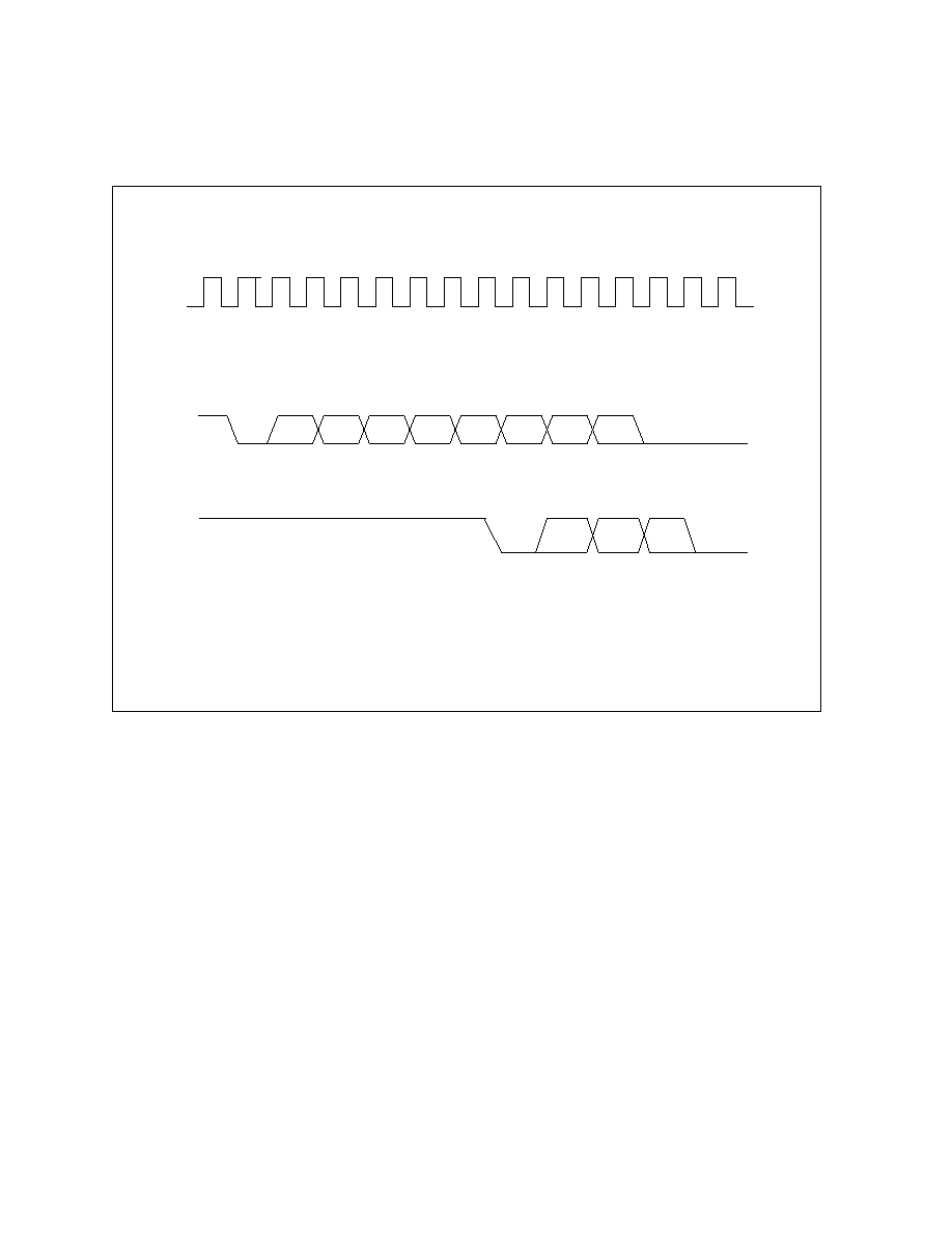
SMSC DS SLC90E66
Page 163
Rev. 07/10/2002
expansion agent. The PCI DMA expansion agent can provide DMA service or ISA Bus Master service using the
SLC90E66 DMA controller. The nREQ/nGNT pair must follow the PC/PCI serial protocol.
8.5.1.1
PCI DMA Expansion Protocol
The PCI expansion agent must support the PCI Expansion Channel Passing Protocol for nREQ and nGNT as shown
in FIGURE 2 PC/PCI SERIAL DMA PROTOCOL.
FIGURE 2 PC/PCI SERIAL DMA PROTOCOL
The device requesting service must encode the channel request information as shown above, where CH0CH7 are
one clock active high states representing DMA channel requests 07. The SLC90E66 encodes the granted channel
on the nGNT line as shown above, where the bits have the same meaning as shown in Table 20 - Address Shifting
for 16-bit DMA Transfers. For example, the sequence [start, bit 0, bit 1, bit 2]=[0,1,0,0] grants DMA channel 1 to the
requesting device, and the sequence [start, bit 0, bit 1, bit 2]=[0,0,1,1] grants DMA channel 6 to the requesting
device.
All PCI DMA expansion agents must use the channel passing protocol described above. They must also work as
follows:
1. If a PCI DMA expansion agent has more than one request active, it must resend the request after it has
completed its transfer for one of the requests. The expansion device should negate its nREQ for two clocks and
then transmit the serial channel passing protocol again, even if there are no new requests from the PCI expansion
agent. For example: If a PCI expansion agent had active requests for DMA channel 1 and channel 5, it would
pass this information to the SLC90E66 through the expansion channel passing protocol. After completing a
transfer for channel 5 (device stops driving request to PCI expansion agent) it must then re-transmit the
expansion channel passing protocol to inform the SLC90E66 that DMA channel 1 was still requesting the bus,
even if that was the only request the expansion device had pending.
2. If an expansion agent's request goes inactive before the SLC90E66 asserts nGNT, it must resend the expansion
channel passing protocol to update the SLC90E66 with the new request information. For example, if an expansion
agent has request pending on DMA channel 1 and 2, it will send them serially to the SLC90E66 using the
expansion channel passing protocol. If, however, DMA channel 1 goes inactive into the expansion agent before
the expansion agent receives a nGNT from the SLC90E66, the expansion agent must negate its nREQ for one
PCICLK
REQ#
Start
CH0
CH1
CH2
CH3
CH4
CH5
CH6
CH7
GNT#
Start
Bit0
Bit1
Bit2

SMSC DS SLC90E66
Page 164
Rev. 07/10/2002
clock and resend the expansion channel passing information with only DMA channel 2 active. The SLC90E66
does not do anything special for this case because a negated DREQ prior to receipt of nDACK is not a valid
condition in the ISA DMA protocol and is not supported in PC/PCI. This requirement is necessary to support Plug-
n-Play ISA devices that toggle nDREQ lines to determine if those lines are free in the system.
3. If an expansion agent has sent its serial request information and receives a new DMA request before receiving
nGNT the agent must resend the serial request with the new request active. For example, if an expansion agent
has requested service from DMA channel 1 and 2 and sees DREQ 3 asserted prior to receipt of GNT, the device
must negate its nREQ for one clock and resend the expansion channel passing information with all three
channels active.
The three cases above require the the PCI DMA expansion device:
1) Negate nREQ for one clock to signal new request information.
2) Negate nREQ for two clocks to signal that a previously granted request has gone inactive.
3) The nREQ and nGNT state machines must run independently and concurrently such that a nGNT could be
received while in the middle of sending a serial nREQ or a nGNT could be asserted while nREQ is negated.
8.5.1.2
PCI DMA Expansion Cycles
The SLC90E66 support of the Mobile PC/PCI DMA Protocol consists of four types of cycles: Memory to I/O, I/O to
Memory, Verify, and ISA Master. ISA Masters are supported through the use of a DMA channel that has been
configred for cascade mode. Single Transfer Mode is supported as the case where the DMA controller negates the
nDACK/nGNT signal after one transfer has been completed or the DMA controller toggles nDACK after every
transfer. Single transfer mode does not require that the requesting device negate nDREQ after a cycle has
completed. Therefore, a PCI DMA device that uses this mode must also sample the nGNT signal and remove nDACK
to the I/O DMA device when nGNT is negated.
For PC/PCI DMA agents, the DMA controller performs a two-cycle transfer (a load followed by a store) as opposed to
the ISA "fly-by" cycle. During the memory portion of the cycle, a PCI memory read or memory write bus cycle is
performed. During the I/O portion of the DMA cycle a PCI I/O cycle to one of four I/O addresses is performed as
shown in Table 21. These cycles must be qualified by an asserted nGNT signal to the requesting device.
Table 21 - I/O Addresses for PC/PCI DMA Cycles
DMA CYCLE TYPE
DMA I/O ADDRESS
TC (A2)
PCI CYCLE TYPE
Normal
00h
0
I/O Read/Write
Normal TC
04h
1
I/O Read/Write
Verify
0C0h
0
I/O Read
Verify TC
0C4h
1
I/O Read
During PCI DMA cycles, the I/O address indicates the type of DMA cycle taking place (whether it is a normal or a
verify cycle, and if this is the last transfer of the buffer). The A2 address line is encoded to indicate the terminal count
signal for PCI cycles such that A2 is asserted during a PCI I/O cycle to indicate the last transfer in the current DMA
buffer. To ensure that non-compliant PCI I/O devices do not confuse Mobile PC/PCI DMA cycles for normal I/O
cycles, the addresses used by the PCI DMA cycles correspond to the slave addresses of the Mobile PC/PCI DMA
controller.
All PCI DMA I/O ports must be DWord aligned and can be sized as either byte or word requiring that any PCI DMA
I/O port always be connected to the lower data lines of the PCI data bus. The byte enables must also reflect the bus
alignment during the I/O portion of a PCI DMA cycle.
Table 22 shows the byte enable and Address/Data signal usage for PCI DMA cycle:

SMSC DS SLC90E66
Page 165
Rev. 07/10/2002
Table 22 - Byte Enable and Address/Data Signal Usage for PC/PCI DMA
DMA CYCLE TYPE
PORT SIZE
PCI ADDRESS/DATA
SIGNALS USED
BE[3-0]
1
8-bit DMA
Byte
AD[7-0]
1110
16-bit DMA
Word
AD[15-0]
1100
1. For verify cycles the value of the Byte Enables (BEs) is a "don't care."
Every DMA device (including Secondary Bus Arbiters) must recognize the combination of a valid nGNT combined
with the DMA I/O address as its command authorization to initiate a DMA access cycle. The SLC90E66 is required to
assert device's nGNT signal until the data phase of the I/O portion of the DMA transfer.
8.5.2
DISTRIBUTED DMA (DDMA)
The Distributed DMA scheme is based on a concept that the registers associated with individual DMA channel can
physically reside on other PCI devices external outside to the SLC90E66. The DDMA logic in the SLC90E66 is used
only when the CPU accesses the 8237 registers. It is the responsibility of the PCI peripheral to perform the data
movement.
The SLC90E66 contains two registers to indicate the I/O locations for the relocated DMA registers. The first register
indicates the offset of the register associated with DMA channels 0-3. The second indicates the offset of the register
associated with DMA channels 5-7. BIOS or other configuration software must program the DDMA peripherals to the
corresponding locations.
8.5.2.1
DDMA Read Cycles Protocol
The SLC90E66 responds to PCI read cycles corresponding to distributed DMA channels by performing the followng
actions:
§
The SLC90E66 issues a PCI retry to terminate the PCI cycle.
§
Immediately, the SLC90E66 will request the PCI bus. Upon grant of the bus, the SLC90E66 will perform one or
more read cycles to the 8237 and/or the PCI peripherals. The I/O location of the read cycle is calculated based
on the following parameters: (1) the DDMA Base Pointer registers in the PCI configuration space, (2) the DMA
channel number (0-3, 5-7), and (3) the register location (0h-Fh).
§
The SLC90E66 will use the data obtained from the read cycles (along with the values from the 8237) to construct
the proper data value.
§
The SLC90E66 releases the PCI bus.
§
When CPU retries the PCI read cycles, the SLC90E66 will respond with the proper data value.
If another PCI master attempts to read or write to one of the DMA controller's registers while a Distributed DMA cycle
is in progress, that cycle will be retried until the current operation completes. This prevents two outstanding PC/PCI
requests.
8.5.2.2
DDMA Write Cycles Protocol
The SLC90E66 responds to PCI write cycles corresponding to distributed DMA channels by performing the following
actions:
§
The SLC90E66 will latch the data and issue a PCI retry to terminate the PCI cycle.
§
Immediately, the SLC90E66 will request the PCI bus. Upon being grant of the bus, the SLC90E66 will perform
one or more write cycles to the 8237 and/or the PCI peripherals. The I/O location of the write cycle is calculated
based on the following parameters: (1) the DDMA Base Pointer registers in the PCI configuration space, (2) the
DMA channel number (0-3,5-7), and (3) the register location (0h-Fh).
§
The SLC90E66 will use the data obtained from the CPU's original write cycles to determine the proper values to
write to the peripherals and to the 8237.
§
The SLC90E66 releases the PCI bus.
§
When CPU retries the PCI read cycles which the SLC90E66 will terminate normally.
If another PCI master attempts to read or write to one of the DMA controller's registers while a Distributed DMA cycle
is in progress, that cycle will be retried until the current operation completes. This prevents two outstanding PC/PCI
requests.

SMSC DS SLC90E66
Page 166
Rev. 07/10/2002
8.5.2.3
I/O Address Calculation
When the SLC90E66 attempts to access the PCI peripherals, it has to first get the exact I/O address for performing
I/O read or write cycles. This I/O address is constructed as follows:
Bits 31-16 are 00h.
Bits 15-6
The value of these bits reflect the value of the Base Pointer in the PCI configuration space for function 0. The
Base Pointer at offset 92h is for channels 0-3. The Base Pointer at offset 94h is for DMA channels 5-7.
Bits 5-4
This field is determined by the DMA channel being accessed.
DMA CHANNEL
NUMBER
BITS[5-4]
0
00
1 or 5
01
2 or 6
10
3 or 7
11
Bits 3-0
This field is determined by the register being accessed.
Table 23 shows the mapping of the 8237 registers to the Distributed DMA peripherals.
Table 23 - Mapping of 8237 Registers to Distributed DMA Peripherals
I/O ADDRESS
8237
F/F
STATUS
R/W
REGISTER NAME
"DISTRIBUTED" CYCLE I/O
ADDRESS
0, 2, 4, 6h,
C4, C8, CCh
0
W
Base Address Register A0-A7
Base Pointer + Channel # + 0h
0, 2, 4, 6h,
C4, C8, CCh
0
R
Current Address Register A0-A7
Base Pointer + Channel # + 0h
0, 2, 4, 6h,
C4, C8, CCh
1
W
Base Address Register A8-A15
Base Pointer + Channel # + 1h
0, 2, 4, 6h,
C4, C8, CCh
1
R
Current Address Register A8-
A15
Base Pointer + Channel # + 1h
87, 83, 81, 82,
8B, 89, 8Ah
x
R/W
Page Register
Base Pointer + Channel # + 2h
1, 3, 5, 7h, C6,
CA, CEh
0
W
Base Word Count Register D0-
D7
Base Pointer + Channel # + 4h
1, 3, 5, 7h, C6,
CA, CEh
0
R
Current Word Count Register
D0-D7
Base Pointer + Channel # + 4h
1, 3, 5, 7h, C6,
CA, CEh
1
W
Base Word Count Register D8-
D15
Base Pointer + Channel # + 5h
1, 3, 5, 7h, C6,
CA, CEh
1
R
Current Word Count Register
D8-D15
Base Pointer + Channel # + 5h
08h, D0h
X
W
Command Register
Base Pointer + Channel # + 8h
08h, D0h
X
R
Status Register
Base Pointer + Channel # + 8h
09h, D2h
X
W
Request Register
Base Pointer + Channel # + 9h
0Bh, D6h
X
W
Mode Register
Base Pointer + Channel # + Bh
0Dh, DAh
X
W
Master Clear
Base Pointer + Channel # + Dh
0Fh, DEh
X
W
Write All Masks Register
Base Pointer + Channel # + Fh
Ah, D4h
X
W
Single Channel Mask
See Note 1
Eh, DCh
X
W
Clear Mask Register
See Note 2

SMSC DS SLC90E66
Page 167
Rev. 07/10/2002
Note 1: Single Channel Mask Register
The Distributed DMA specification doesn't require that the peripherals implement the Single Channel Mask Registers.
Instead, a write to the Single Channel Mask register will cause a write to the Write All Masks Register which has a
separate mask bit for each channel. The Distributed DMA peripheral uses bit 0 in the Write All Masks Register for that
particular channel.
When a write occurs to the Single Channel Mask registers, the SLC90E66 will examine the low two data bits to
determine the DMA channel number. The SLC90E66 will generate a write to the peripheral device at (Base Pointer +
Channel # + Fh). The data value of bit 0 for that write cycle will be determined by data bit 2 of the original CPU write.
Note 2: Clear Mask Register
The Distributed DMA specification doesn't require that the peripherals implement the Clear Mask Command. Instead,
a write to the Clear Mask Command register will cause writes to all the distributed channels associated with that
8237.
When a write occurs to the Clear Mask Command register, the SLC90E66 will perform up to 4 writes to the Write All
Masks register (Base Pointer + Channel # + Fh) with a data value of 0h.
8.6 Interrupt
Controller
The SLC90E66 integrates an ISA compatible interrupt controller that incorporates the functionality of two 8259
interrupt controllers. The two interrupt controllers are cascaded. The master controller provides IRQ[7-0] and the
slave controller provides IRQ[15-8]. There are three interrupts used for internal functions only. IRQ0 is used as a
system timer interrupt and is tied to interval Timer 1, Counter 0. IRQ0 is available to the user only if an external IO
APIC is enabled. IRQ2 is used to cascade the two controllers together and is not available to the user. IRQ13 is
connected internally to nFERR. There are 13 interrupt lines (IRQ1, IRQ3-IRQ12, IRQ14, IRQ15) available for external
uses. Edge or level trigger modes of operation can be programmed independently for each channel. Note that when
bit 4 of the XBCS register is set to 1, the IRQ12/M is generated internally as part of the mouse support. When this bit
is set to 0, standard IRQ12 function is provided and IRQ12 is available externally.
The two 8259 cores, Interrupt Controller 1 and Interrupt Controller 2, are initialized separately and can be
programmed to operate in different modes. The default settings are 80x86 Mode, Edge Sensitive Detection, Normal
EOI, Non-Buffered Mode, Special Fully Nested Mode disabled, and Cascade Mode. Controller 1 is configured as the
Master Interrupt Controller and controller 2 is connected as the Slave Interrupt Controller.
Interrupt steering is supported allowing the four PCI active low interrupts (nPIRQ[A-D]) to be internally routed to one
of 11 interrupts (IRQ[15-14,12-9,7-3]).
8.6.1
PROGRAMMING THE INTERRUPT CONTROLLER
The interrupt controller accepts two types of command words generated by the CPU or bus master: Initialization
Command Words and Operation Command Words.
8.6.1.1
Initialization Command Words (ICWs)
The interrupt controller must be initialized before normal operation can begin. The SLC90E66 interrupt controllers
require a four-byte sequence to configure the controller correctly.
The four initialization command words are referred to by their acronyms: ICW1, ICW2, ICW3, and ICW4. The base
address for each Interrupt Controller is at a fixed I/O location: 0020h for Controller 1 and 00A0h for Controller 2. An
I/O write to the Controller 1 or Controller 2 base address with data bit 4 equal to 1 is interpreted as ICW1. To
complete the initialization, the SLC90E66 requires three I/O writes to "base address +1" (21h for Controller 1 and A1h
for Controller 2) to follow the ICW1. The first write performs ICW2, the second write performs ICW3 and the third write
performs ICW4.
The four commands are summarized as follows:
§
ICW1 starts the initialization sequence for the controller.
§
ICW2 programs the value of bits[7-3] of the interrupt vector that will be released onto the data bus during an
interrupt acknowledge cycle. A different base [7-3] is selected for each interrupt controller.
§
ICW3 has different meaning for two controllers:

SMSC DS SLC90E66
Page 168
Rev. 07/10/2002
1) For Controller 1, the master controller, ICW3 is used to indicate which IRQx input line is used to cascade the
slave controller. In the SLC90E66 implementation, IRQ2 of the master controller is used to cascade the INTR
output of the slave controller. Therefore, bit 2 of ICW3 on Controller 1 is set to 1, and the other bits are all set to
0's.
2) For Controller 2, ICW3 is the slave identification code used during an interrupt acknowledge cycle. Controller 1
broadcasts a code to Controller 2 over three internal cascade lines if an IRQ[x] line of Controller 2 won the
priority arbitration on the master controller and was granted an interrupt acknowledge by the CPU. If this
identification code is equal to bits[2-0] of ICW3, Controller 2 will broadcast the interrupt vector during the second
interrupt acknowledge cycle.
§
ICW4 must be programmed on both controllers. At the very least, bit 0 must be set to a 1 to indicate that the
controllers are operating in an 80x86 based system.
8.6.1.2
Operation Command Words (OCWs)
These are the command words which dynamically reprogram the interrupt controllers to operate in various interrupt
modes. The OCWs can be written into the Interrupt Controller any time after initialization
OCW1 can be used to mask interrupt lines. Writing a 1 in any bit of this command word will mask incoming interrupt
requests on the corresponding IRQx line.
OCW2 is used to control the rotation of interrupt channel priorities when operating in the rotating priority mode. It can
also control the End of Interrupt (EOI) function of the controller.
OCW3 is used to set up reads of the ISR and IRR, to enable or disable the Special Mask Mode, and to set up the
interrupt controller in Poll Command Mode.
8.6.2
END OF INTERRUPT OPERATION
The In Service (IS) bit can be set to 0 automatically following the trailing edge of the second nINTA pulse when the
Automatic EOI mode is enabled or by a command word that must be issued to the interrupt controller before returning
from a service routine (EOI command). An EOI command must be issued twice, once for the master and once for the
slave.
There are two forms of EOI commands: Specific and Non-Specific. When the Interrupt Controller is operated in fully
nested modes, it can determine which IS bit to set to 0 on EOI. When a Non-Specific EOI command is issued, the
interrupt controller will automatically set to 0 the highest IS bit of those that are set to 1, since in the fully nested mode
the highest IS level was necessarily the last level acknowledged and serviced. A non-specific EOI can be issued with
OCW2 (EOI=1, SL=0, and R=0).
When a mode is used which may disturb the fully nested structure, the interrupt controller may no longer be able to
determine the last level acknowledged. In this case, a Specific End Of Interrupt must be issued which states the IS
level to be reset. A Specific EOI can be issued with OCW2 (EOI=1, SL=1, R=0, and L0-L2 specifies the IS bit to be
reset to 0 in binary format).
An IS bit that is masked by an IMR bit will not be cleared by a non-specific EOI if the Interrupt Controller is in the
Specific Mask Mode.
Automatic End of Interrupt (AEOI) Mode
If AEOI is 1 in ICW4, then the interrupt controller will operate in AEOI mode continuously until reprogrammed by
ICW4. To reprogram ICW4 requires that ICW1, ICW2 and ICW3 must be reprogrammed first. In AEOI mode, the
interrupt controller will automatically perform a non-specific EOI operation at the trailing edge of the last interrupt
acknowledge pulse. This mode should be used only when a nested multi-level interrupt structure is not required
within a single interrupt controller. Consequently, the AEOI mode can only be used in the master interrupt controller
(controller 1) and not a slave controller (controller 2).

SMSC DS SLC90E66
Page 169
Rev. 07/10/2002
8.6.3
MODES OF OPERATION
8.6.3.1
Fully Nested Mode
This is the default operating mode after initialization unless another mode is programmed. The interrupt requests are
ordered in priority from 0 through 7, with 0 being the highest priority. Priority can be changed when rotating priority
mode is selected.
When an interrupt is acknowledged by the CPU, the highest priority request is determined and its vector is placed on
the bus. Additionally, a bit of the Interrupt Service Register (IS[0-7]) is set, and it remains set until the CPU issues an
EOI command immediately before returning from the interrupt service routine. Or, if the AEOI bit is set, this IS bit
remains set until the trailing edge of the second nINTA pulse. While the IS bit is set, all further interrupts of the same
or lower priority are inhibited. Interrupt requests with higher priority level will generate an interrupt, but it will be
acknowledged only if the CPU internal interrupt enable control has been re-enabled by the software.
8.6.3.2
Special Fully Nested Mode
This mode is used in the case of a system where cascading is used, and the priority has to be conserved within each
slave. The master controller is programmed to be in the Special Fully Nested Mode using ICW4. This mode is similar
to the normal nested mode with the following exceptions:
§
When an interrupt request from a certain slave is in service, this slave is not locked out from the master's priority
logic and further interrupt requests from higher priority IRQs within the slave will be recognized by the master
and will initiate interrupt to the CPU. While in the normal nested mode, a slave is masked out when its request is
in service and no higher requests from the same slave can be serviced.
§
When exiting the interrupt service routine, the software has to check whether the interrupt serviced was the only
one from that slave. This is done by sending a non-specific EOI command to the slave and then reading its In-
Service Register and checking for zero. If no bit is set, a non-specific EOI can be sent to the master too. If it is
not zero, no EOI should be sent.
8.6.3.3
Automatic Rotation Mode (Equal Priority Devices)
Automatic rotation mode provides for a sequential 8-way rotation. In this mode, a device receives the lowest priority
after being serviced. In the worst case, a device requesting an interrupt will have to wait until each of seven other
devices are serviced once.
There are two ways to accomplish automatic rotation using OCW2: the Rotation on Non-Specific EOI command (R=1,
SL=0, and EOI=1) and the Rotation in Automatic EOI Mode which is set by (R=1, SL=0, and EOI=0) and cleared by
(R=0, SL=0, and EOI=0).
8.6.3.4
Specific Rotation Mode (Specific Priority Devices)
The programmer can change priorities by selecting the bottom priority and thus fixing all other priorities. For example,
if IRQ6 is programmed as the bottom priority device, then IRQ7 will be the highest priority device.
The Set Priority Command is issued in OCW2 with R=1, SL=1 and L0-L2 is the binary code of the bottom priority
device.
Note that, in this mode, internal status is updated by software control during OCW2. However, it is independent of the
EOI command. Priority changes can be executed during an EOI command by using the Rotate on Specific EOI
command in OCW2 with R=1, SL=1, EOI=1, and L0-L2 is the binary code of the IRQ channel to receive bottom
priority.
8.6.3.5 Polled
Mode
The Polled Mode can be used to conserve space in the interrupt vector table. Multiple interrupts that can be serviced
by one interrupt service routine do not need separate vectors if the service routine uses the poll command.
The Polled Mode can also be used to expand the number of interrupts. The polling interrupt service routine can call
the appropriate service routine, instead of providing the interrupt vectors in the vector table.
In the Polled mode, the INTR output is not used and the CPU internal interrupt Enable control is reset, disabling its
interrupt input. Services to devices is achieved by software using a Poll Command.
The Poll Command is issued by setting P=1 in OCW3. The interrupt controller treats the next I/O read pulse to the
interrupt controller as an interrupt acknowledge, sets the appropriate IS bit if there is a request, and reads the priority
level. Interrupts are frozen from the I/O write to the I/O read.

SMSC DS SLC90E66
Page 170
Rev. 07/10/2002
This mode is useful if there is a routine command common to several levels so that the nINTA sequence is not
needed.
8.6.4 CASCADE
MODE
The SLC90E66's interrupt controllers are interconnected in a cascade configuration with one master and one slave.
There are 15 separate priority levels (IRQs). The master controls the slave through a three-line internal cascade bus.
When the master drives 010b on the internal cascade bus, this bus acts like a chip select to the slave controller.
In a cascade configuration, the slave interrupt outputs are connected to the master interrupt request inputs. When a
slave request line is activated and then acknowledged, the master will enable the corresponding slave to release the
interrupt vector address during the second nINTA cycle of the interrupt acknowledge sequence.
Each interrupt controller in the cascaded system must follow a separate initialization sequence and can be
programmed to work in a different mode. An EOI command must be issued twice, one for the master and another one
for the slave.
8.6.5
EDGE AND LEVEL TRIGGERED MODE
In ISA compatible systems the triggered mode is selected using bit 3 in ICW1. The SLC90E66 disables this bit and
adds two new registers, ELCR1 and ELCR2, for edge and level triggered mode selection for the two controllers. The
default programming is equivalent to programming the LTIM bit (bit 3 of ICW1) to a 0 (edge triggered mode for all
interrupts). Note that IRQ0, 1, 2, 8 and 13 can not be programmed for level sensitive mode and can not be modified
by software.
When an ELCR bit is set to 0, an interrupt request will be recognized by a low to high transition on the corresponding
IRQx input. The IRQ input can remain high without generating another interrupt.
When an ELCR bit is set to 1, an interrupt request will be recognized by a low level on the corresponding IRQ input.
The interrupt request must be removed before the EOI command is issued to prevent a second interrupt from
occurring.
In either triggered mode, the IRQ inputs must remain active until after the falling edge of the first nINTA. If the IRQ
input goes inactive before this time, a default "IRQ7" will occur when the CPU acknowledges the interrupt. To
implement this feature, the IRQ7 routine is used for "clean up" simply executing a return instruction, thus ignoring the
interrupt. If IRQ7 is needed for other purposes, a default IRQ7 can still be detected by reading the ISR. A normal
IRQ7 interrupt will set the corresponding ISR bit, while a default IRQ7 will not set this bit. If a default IRQ7 routine
occurs during a normal IRQ7 routine, the ISR will remain set. In this case, it is necessary to keep track of whether or
not the IRQ7 routine was previously entered. If another IRQ7 occurs, it is a default.
8.6.6 INTERRUPT
MASKS
Masking on an Individual Interrupt Request Basis
Each interrupt request input can be masked individually by the Interrupt Mask Register (IMR). This register is
programmed through OCW1. Each bit in the IMR masks one interrupt channel, when it is set to 1. Masking an IRQ
channel does not affect other channel's operation, with one exception. Masking IRQ2 on Controller 1 will mask off all
requests for service from Controller 2 because the Controller 2's INTR output is directly connected to the Controller
1's IRQ2 input.
Special Mask Mode (SMM)
Some applications may require an interrupt service routine to dynamically alter the system priority
structure during its execution. For example, the routine may wish to inhibit lower priority requests for a
portion of its execution but enable some of them for another portion. The difficulty is that if an Interrupt
Request is acknowledged and an End of Interrupt command did not reset its IS bit (i.e., while executing a
service routine), the Interrupt Controller would have inhibited all lower priority requests with no easy way
for the routine to enable them.
The Special Mask Mode enables all interrupts not masked by a bit set in the Mask Register. Interrupt Service
Routines that require dynamic alteration of interrupt priorities can take advantage of the Special Mask Mode. For
example, a service routine can inhibit lower priority requests during a part of the interrupt service routine, then enable
some of them during another part.

SMSC DS SLC90E66
Page 171
Rev. 07/10/2002
In the Special Mask mode, if a mask bit is set to 1 in OCW1, it inhibits further interrupts at that level and enables
interrupts from all other levels that are not masked. Therefore, any interrupts may be selectively enabled by loading
the Mask Register with an appropriate pattern. Without Special Mask Mode, the interrupt controller inhibits all lower
priority requests until an EOI is issued to clear the IS bit. The Special MaskMode provides an easy way for the
service routine to selectively enable only the interrupts needed by loading the Mask register.
The Special Mask Mode is set by OCW3 with SSMM=1, and SMM=1. The SMM can be cleared by OCW3 with
SSMM=1, and SMM=0.
8.6.7
INTERRUPT CONTROLLER STATUS
The Interrupt Request Register (IRR) and In-Service Register (ISR) can be read via OCW3. The Interrupt Mask
Register (IMR) is read through a read of OCW1.
IRR - This 8-bit register contains the status of each interrupt request line. Bits that are clear indicate interrupts that
have not requested service. The interrupt controller clears the IRR's highest priority bit during an interrupt
acknowledge cycle. Prior to reading IRR, a Read Register Command must be issued with OCW3 (RR=1, RIS=0)
ISR - This 8 bit register indicates the priority levels currently receiving service. Bits that are cleared indicate interrupt
request lines that have not been asserted, or interrupt requests that have not been acknowledged. Bits that are set
indicate interrupts that have been acknowledged and their service routine started. Only the highest priority interrupt
service routine executes at any time because the lower priority interrupt services are suspended while higher priority
interrupts are serviced. The ISR is updated when an EOI command is issued. Prior to reading ISR, a Read Register
Command must be issued with OCW3 (RR=1, RIS=1)
IMR - This 8 bit register indicates which interrupt request lines are masked. OCW1 is used for reading the IMR.
The interrupt controller retains the ISR/IRR status read selection following each write to OCW3. Therefore, there is no
need to write an OCW3 before every status read operation, as long as the current status read corresponds to the
previously selected register. After initialization the interrupt controller is set to read the IRR.
8.6.8 INTERRUPT
STEERING
The SLC90E66 allows four PCI interrupts (nPIRQ[AD]) to be internally routed to one of 11 interrupts: 3-7, 9-12, 14
or 15. The nPIRQx lines are run through an internal multiplexer that routes an individual nPIRQx line to any one of 11
IRQ inputs. The assignment is programmable through the nPIRQx Route Control Registers. One or more nPIRQx
lines can be routed to the same IRQx input. PCLK is used to synchronize the nPIRQx inputs.
Bits [3-0] in each PIRQx Route Control register are used to route the associated nPIRQx line to an
internal IRQ input. Bit 7 in each register is used to disable routing of the associated nPIRQx.
The nPIRQx lines are defined as active low, level sensitive to allow multiple interrupts on a PCI board to share a
single line. The software must change an IRQ to level sensitive mode if a nPIRQx is routed to that IRQ line. The
selected IRQ can no longer be used by an ISA device even if that ISA device can respond as an active low level
sensitive interrupt.
8.7 Serial Interrupts (SIRQ)
The SLC90E66 supports a serial Interrupt scheme that allows a single signal to be used to report ISA-style interrupt
requests. Serial Interrupt scheme is typically used by docking bridges or Cardbus bridges in a mobile system.
Because more than one device may need to share the single IRQ signal, an Open Collector signaling scheme is
used. Serial Interrupt timing is based on the PCI clock. If the PCI clock is inactive when a device needs to signal an
interrupt, the nCLKRUN signal must first be asserted by the device to restart the PCI clock.
8.7.1 SIRQ
PROTOCOL
Serial interrupt information is transferred using three types of frames: a Start Frame, one or more IRQ data frames,
and one Stop frame. There are two modes of operation: Quiet Mode and Continuous Mode.
8.7.1.1
Quiet (Active) Mode
The peripheral asserts the SERIRQ signal for one clock, and then tri-states it to indicate an interrupt. This brings all
the state machines to the active state.

SMSC DS SLC90E66
Page 172
Rev. 07/10/2002
The SLC90E66 will then take control of the SERIRQ signal by driving it low on the next clock, and will continue
driving it low for 3-7 (programmable) more clocks, which makes the total number of clocks low from 4 to 8. After those
clocks, the SLC90E66 will drive SERIRQ high for one clock and then tri-states the signal.
8.7.1.2
Continuous (Idle) Mode
In this mode, the SLC90E66 (rather than the peripherals) initiates the START frame. Typically, this will be done to
update IRQ status (acknowledges). The SLC90E66 will drive SERIRQ low for 4 to 8 clocks. Continuous mode is the
default mode after reset, and can be used to enter the Quiet mode.
8.7.1.3 Data
Frame
Once the Start frame has been initialized, all of the serial interrupt peripherals must start counting frames based on
the rising edge of SERIRQ. Each of the IRQ/DATA frames has exactly 3 phases of 1 clock each: a Sample phase, a
Recovery phase, and a Turn-around phase.
During the Sample phase, the device drives SERIRQ low if the corresponding interrupt signal should be active. If the
corresponding interrupt is inactive, then the device should not drive the SERIRQ signal line. The external pull-up
resistor will keep the signal high to indicate an inactive IRQ request. During the other two phases (Turn Around and
Recovery), no device should drive the SERIRQ signal line.
Table 24 shows the supported IRQ signals and the specific ordering of these signals in the SIRQ data frames
protocol.
Table 24 - SERIRQ Frames
DATA FRAME NUMBER
USAGE
# CLOCKS PAST START
1
UNASSIGNED
2
2
IRQ1
5
3
nSMI
8
4
IRQ3
11
5
IRQ4
14
6
IRQ5
17
7
IRQ6
20
8
IRQ7
23
9
IRQ8*
26
10
IRQ9
29
11
IRQ10
32
12
IRQ11
35
13
IRQ12
38
14
UNASSIGNED
41
15
IRQ14
44
16
IRQ15
47
17
nIOCHCK
50
18
nPCI INTA
53
19
nPCI INTB
56
20
nPCI INTC
59
21
nPCI INTD
62
32:22
UNASSIGNED
96
*Note: This is controlled by IRQ8 Source Register (Function 0, Offset 66h), in section titled 4.1.13 IRQ8SR - IRQ8
Source Register (Function 0).
If an nSMI is active on frame 3, the SLC90E66 will drive its nEXTSMI signal active, which will then cause an nSMI to
the CPU if enabled.

SMSC DS SLC90E66
Page 173
Rev. 07/10/2002
8.7.1.4 Stop
Frame
After all of the data frames are complete, a Stop Frame will be issued by the SLC90E66. This is performed by pulling
SERIRQ low for 2-3 clocks. The number of clocks determines the next working mode:
§
If the Stop Frame duration is 2 clocks, the next mode is the Quiet mode. Any device may initiate a
Start Frame in the second clock (or later) after the rising edge of the Stop Frame.
§
If the Stop Frame duration is 3 clocks, the next mode is the Continuous mode. Only the SLC90E66
may initiate a Start Frame in the second clock (or later) after the rising edge of the Stop Frame.
8.8 Timer/Counters
The SLC90E66 integrates an 8254 equivalent programmable interval timer, which contains three counters. Each
counter output provides a key system function. Counter 0 is internally connected to IRQ0 and provides a system timer
interrupt event for a time-of-day, diskette time-out, or other system timing functions. Counter 1 generates a refresh
request signal to refresh ISA memory device. Counter 2 generates the tone for the speaker. The counters normally
use the 14.31818 MHz OSC as a clock source.
8.8.1 COUNTER
0
This counter functions as the system timer by generating IRQ0 periodically and is typically programmed for Mode 3
operation. The counter produces a square wave with a period equal to the product of the counter period, which is
838ns, and the initial count value. The counter loads the initial count value one counter period after software writes
the count value to the counter I/O address. The counter initially asserts IRQ0 and decrements the count value by two
each counter period. The counter negates IRQ0 when the count value reaches 0. It then reloads the initial count
value and again decrements the initial count value by two each counter period. The counter then asserts IRQ0 when
the count value reaches 0, reloads the initial count value, and repeats the cycle, alternately asserting and negating
IRQ0.
8.8.2 COUNTER
1
The SLC90E66 does not implement a programmable Counter 1. Instead, a fixed refresh counter has been
implemented to provide the refresh request signal with a fixed 15
µ
s intervals, operating in Mode 2. The counter
negates refresh request for 520ns. The refresh interval can be extended from 15
µ
s to 228
µ
s by setting AT DRAM
Slow Refresh bit (bit 0 of SBMISCL register, Configuration Space Offset E0h (see section 4.1.24).
8.8.3 COUNTER
2
This counter provides the speaker tone and is typically programmed for Mode 3 operation. The counter provides a
frequency equal to the counter clock frequency, which is 1.193MHz, divided by the initial count value. The speaker
output must be enabled by a write to port 061h.
8.8.4
THE INTERVAL TIMER PROGRAMMING INTERFACE
The counter/timers are programmed via I/O accesses and are addressed as though they were contained in a single
8254. The timer uses a single Control Word Register to control the operation of all three counters. The Control Word
Register is write-only.
The interval timer is an I/O mapped device. Several commands are available:
§
The Control Word Command specifies which counter to read or write, the operating mode, and the count
format (binary or BCD)
§
The Counter Latch Command latches the current count so that it can be read by the system. The countdown
process is not affected by the latch command.
§
The ReadBack Command reads the count value, programming mode, the current state of the OUT pins, and
the state of the Null Count Flag of the selected counter.
The Read/Write logic selects the Control Word Register during an I/O write when address lines A[1-0]=11b. This
condition occurs during an I/O Write to address 043h. When the CPU writes to port 43h, the data is stored in the
Control Word Register and is interpreted as the Control Word used to define the operation of the Counters.

SMSC DS SLC90E66
Page 174
Rev. 07/10/2002
After power up, the timer counters stay in an unknown state. It is recommended to program the timer counter
immediately after power up.
8.8.4.1 Write
Operations
Programming the interval timer is very straight forward: First write a control word, then write an initial count for each
counter by loading the least and/or most significant bytes (as required by Control Word bits 5, 4) of the 16-bit counter.
The control word must be written before the initial count is written. And the initial count must follow the count format
specified in the control word: least significant byte only, most significant byte only, or least significant byte first and
then most significant byte.
Since the Control Word Register and the three counters have separate addresses (selected by the A1 and A0
address lines) and each control word specifies the counter it applies to (SC0 and SC1 bits), no special instruction
sequence is required. A new initial count may be written to a counter at any time without affecting the counter's
operating mode. The new count must follow the programmed count format.
When a counter is programmed to read or write two-byte counts, the program must not transfer the control between
accessing the first and second byte to another routine which may also access that same counter.
8.8.4.2
Control Word Format
The control word specifies the counter, the operating mode, the order and size of the count value, and whether it
counts down in a 16-bit or BCD format. After the control word is programmed, a new count can be written at any time.
The new value will take effect according to the programming mode.
8.8.4.3 Read
Operations
There are three possible ways for reading the counters: a simple read operation, the Counter Latch Command and
the ReadBack Command.
Counter I/O Port Read (Simple Read)
To read the counter, the CLK input of the selected counter must be inhibited by using either GATE input or external
logic. Otherwise, the count may be in the process of changing while it is read, giving an undefined result. Within the
timer unit, the GATE inputs of Counter 0 and Counter 1 are tied high. Therefore, Simple Read should not be used on
these two counters. The GATE input of Counter 2 is controlled by I/O port 061h. When Counter 2 GATE input is
disabled through this register, I/O reads of port 042h will return correct count value.
Counter Latch Command
This command latches the count at the time the command is received. It ensures that the count read from the counter
is accurate. The count value can be read from each counter's Count Register as was programmed by the Control
Register.
When the Counter Latch Command is received, the selected counter's output latch (OL) latches the count. This count
is held in the latch until it is read by the CPU or till the counter is reprogrammed. The count is then unlatched
automatically and the output latch returns to follow the counting element (CE). This mode allows reading the contents
of the counters "on the fly" without affecting counting in progress.
The Counter Latch Command does not affect the programmed mode of the counter, and it can be used for each of
the three counters.
A Counter Latch Command is only honored by the Counter if the output latch contents of the previous latch command
is read. For example, if a Counter is latched and then, some time later, latched again before the count in the output
latch is read, the second Counter Latch Command is ignored. The count read will be the count at the time the first
Latch Command was issued.
The SLC90E66 timer allows reads and writes of the same counter may be interleaved. For example, if the Counter is
programmed for two byte counts, the following programming sequence is still valid:
1) Read least significant byte
2) Write new least significant byte
3) Read most significant byte
4) Write new most significant byte

SMSC DS SLC90E66
Page 175
Rev. 07/10/2002
Read Back Command
The Read Back command is used to determine the count value, programmed mode, and current states of the OUT
pin and Null Count flag of the selected counter or counters. When the Read Back command is written to the Control
Word Register, the current states of the above mentioned variables are latched. They can be read by I/O access to
the counter address.
The Read Back Command may be used to latch multiple counters at one time. When bit 5 of the Command word is a
0 and multiple counters are selected through bit 1 to bit 3 of the Command word, the single Read Back Command is
functionally equivalent to several Counter Latch Commands, one for each counter latched. Like the Counter Latch
Command, each counter's latched count is held until it is read or until the counter is reprogrammed. Once read, the
counter is unlatched. The other counters remain latched until they are read. If multiple Read Back Commands are
issued to the same counter without reading the count, all but the first are ignored.
The Read Back Command can also be used to latch status information of selected counters by setting bit 4 of the
Command word to a 0. Status has to latch to be read. The status of a counter is accessed by a read from that
counter's I/O port address. If multiple counter status latch operations are performed without reading the status, all but
the first are ignored. The status returned from the read is the counter status at the time the first status Read Back
Command was issued.
It is also possible to latch both count and status of the selected counters simultaneously by setting both bit 5 and bit 4
of the Command word to 0 (bits[5-4]=00b). It is functionally the same as issuing two consecutive, separate Read
Back Commands.
If both count and status of a counter are latched, the first read operation from that counter will return the latched
status, regardless of which was latched first. The next one or two reads, depending on whether the counter is
programmed for one or two byte counts, return the latched count. Subsequent reads return unlatched count.
8.9 Real Time Clock Module
The SLC90E66 contains a Motorola MC146818A-compatible real-time clock module with 256 bytes static RAM as a
date-and-time keeping device with alarm features and battery backed-up operation. The RTC counts seconds,
minutes, hours, days, day of the week, date, month, and year. Leap year compensation is provided.
Three interrupt features are provided by the RTC module: time of day alarm with once-a-second to once-a-month
range, periodic rates of 122
µ
s to 500ms, and end of update cycle notification.
The RTC module contains 256 bytes of battery backed RAM. The memory is divided into two banks, namely, the
standard bank and the extended bank, each with 128 bytes. The standard bank contains 10 bytes indicating time and
date information, 4 bytes used as Control Registers (A, B, C, D), and 114 bytes used as general purpose RAM. The
extended bank has the whole 128 bytes as general purpose RAM.
The RTC also supports two lockable memory ranges. By turning on bits in the configuration register, two 8-byte
space can be locked to read and write accesses, which prevents unauthorized reading of passwords or other security
information.
Time, calendar, and alarm can be represented in either binary or BCD format, determined by bit 2 of Control Register
B. The hour is represented either in 12 or 24 hour format, selected by bit 1 of Control Register B. When changing the
format, the programmer has to reinitialize the time registers to the new data format.
The RTC module is operated on a 32.768Khz crystal and a separate 3V lithium battery that provides up to 7 years of
protection. The clock signal is internally divided down to 1 Hz signal, one of the 15 taps from the divider chain can be
selected as a periodic interrupt.
The RTC can be relocated and disabled for improved performance in mobile applications. This allows the use of an
external RTC implementation in a power manged I/O device.
8.9.1
RTC REGISTERS AND RAM
The RTC internal registers and RAM are organized as two banks of 128 bytes each, called the standard and
extended banks. The first 14 bytes of the standard bank contain the RTC time and date information along with four
registers, A-D, that are used for configuration of the RTC. The extended bank contains a full 128 bytes of battery
backed SRAM, and is accessible even when the RTC module is disabled (through the RTC configuration register).

SMSC DS SLC90E66
Page 176
Rev. 07/10/2002
All data movement between the CPU and the RTC is done through registers mapped to the ISA IO space at locations
70-73h:
IO locations 70h and 71h are the standard ISA locations for the RTC. The RTC location can be changed by
reprogramming the RTC Index Primary Base Address Registers (D4-D5h Revision F and later, D0-D1 Revisions E
and earlier), see section 4.1.22 RTCPBAL - RTC Index Primary Base Address Low Byte. Table 25 shows the address
map for this bank. IO locations 72h and 73h are for accessing the extended RAM, and may be disabled. The location
of the extended bank is also programmable through the RTC Index Primary Base Address Registers.
Table 25 - RTC Standard RAM Bank
INDEX ADDRESS
NAME
00h
Seconds
01h
Seconds Alarm
02h
Minutes
03h
Minutes Alarm
04h
Hours
05h
Hours Alarm
06h
Day of Week
07h
Date of Month
08h
Month
09h
Year
0Ah
Register A
0Bh
Register B
0Ch
Register C
0Dh
Register D
0Eh-7Fh
114 bytes of user RAM
Note:
Both banks are accessed through an indexed scheme: ISA IO addresses 70h/72h are the address pointers
for the standard bank/extended bank respectively. ISA IO addresses 71h/73h are the data registers for the standard
bank/extended bank respectively.
The programmer has to make sure that data stored in these locations is within the reasonable values and represents
a possible date and time. The only exception is to store a value of C0h - FFh in the alarm bytes to indicate a "don't
care" situation. The software must make sure that bit 7 of Control Register A must be read as 0 to avoid the RTC
update process before access to these locations, bit 7 of Control Register B has to set to a 1 before program these
locations to avoid clashes with the RTC update cycle.
The internal RTC registers can only be accessed by PCI masters. ISA master access is not supported.
The address decoding scheme for the RTC is programmed through the RTCCFG register (offset CBh), see section
4.1.21 RTCCFG - Real Time Clock Configuration Register (Function 0). The following table explains the usage of the
internal and external RTC based on the RTC address decoding scheme.
Table 26 - Internal and External RTC Usage
BIT 5 OF RTCCFG
REGISTER (AT CBh)
EXTERNAL RTC ON
PCI BUS
INTERNAL RTC WITH
INDEX BASE = 70H
EXTERNAL RTC ON ISA OR XBUS
0
(Subtractive Decode)
First Priority*.
Second Priority.
Can be used if the
external RTC on PCI
bus did not decode the
RTC access cycles.
Third Priority.
Can be used if external RTC on PCI
bus is not used and internal RTC is
disabled.
1
(Positive Decode)
Not available.
First Priority.
Second Priority.
Can be used if internal RTC is
disabled.

SMSC DS SLC90E66
Page 177
Rev. 07/10/2002
8.9.2 CONTROL
REGISTER
A
Offset Address: 0Ah
Default Value:
NA, this register is not affected by any system reset signal.
Access:
Read/Write
This is a general configuration register.
BIT
FUNCTION
7
Update In Progress (UIP).
1: An update is soon to occur or is in progress.
0: An update cycle will not start for at least 244us. The time, calendar, and alarm information in RAM is
always available when the bit is 0.
This bit may be monitored as a status flag.
6-4
Division Chain Select (DVx). These three bits control the divider chain for the oscillator.
Bits [6-4]
Function
Bits[6-4]
Function
000
Osc disabled
001
Osc disabled.
010
normal function
011
Test mode.
10x
Test mode
11x
Divider reset
3-0
Rate Select Bits (RSx). Selects one of 13 taps of the 15 stage divider chain. The selected tap can
generate a periodic interrupt if the PIE bit is set in register B. Otherwise, this tap will set the PF flag of
register C. If the periodic interrupt is not to be used, these bits should all be set to zero.
Bits [3-0]
Interrupt Frequency
Periodic Rate
0000
0.0
none
0001
256 Hz
3.90625 ms
0010
128 Hz
7.8125 ms
0011
8.192 kHz
122.070
µ
s
0100
4.096 kHz
244.141
µ
s
0101
2.048 kHz
976.5625
µ
s
0110
1.024 kHz
976.5625
µ
s
0111
512 Hz
1.953125 ms
1000
256 Hz
3.90625 ms
1001
128 Hz
7.8125 ms
1010
64 Hz
15.625 ms
1011
32 Hz
31.25 ms
1100
16 Hz
62.5 ms
1101
8 Hz
125 ms
1110
4 Hz
250 ms
1111
2 Hz
500 ms

SMSC DS SLC90E66
Page 178
Rev. 07/10/2002
8.9.3
CONTROL REGISTER B
Offset Address: 0Bh
Default Value:
X0000XXXb.
Access:
Read/Write
This is a general configuration register.
BIT
FUNCTION
7
SET. Enable the update cycles.
0: Update cycles occur normally once a second.
1: The current update cycle will abort and subsequent update cycles will not occur until SET is reset to
zero. When set to 1, the BIOS can initialize time and calendar bytes safely.
This bit is not affected by the nRSMRST (Reset signal asserted during resume from suspension).
6
Periodic Interrupt Enable (PIE).
1: The Periodic Interrupt Enable allows an interrupt to occur with a time base set with the RS bits of
register A.
0: Disables the generation of the periodic interrupt.
This bit is cleared (set to zero) on active nRSMRST.
5
Alarm Interrupt Enable (AIE).
1:
An interrupt will occur when the AF is one as set from an alarm match from the update cycle. An
alarm can occur once a second, one an hour, once a day, or once a month.
0:
Disables the generation of the Alarm interrupt.
This bit is cleared on active nRSMRST.
4
Update-ended Interrupt Enable (UIE).
1:
Allows an interrupt to occur when the update cycle ends.
0:
Disable the generation of the update-ended interrupt.
This bit is cleared on active nRSMRST.
3
Square Wave Enable (SQWE). The bit serves no function in this device, yet is left in the register to
provide compatibility with the Motorola 146818B. There is no SQW output pin assigned on the
SLC90E66.
This bit is cleared on active nRSMRST.
2
Data Mode (DM).
1:
Selects binary as data representation format.
0:
Selects BCD as data representation format.
This bit is not affected by nRSMRST.
1
Hour Mode (HF).
1:
24 hour mode is used.
0:
12 hour mode is selected.
In 12 hour mode, bit 7 of the hour register represents AM as zero and PM as one.
This bit is not affected by nRSMRST.
0
Daylight Savings Enable (DSE). The daylight savings enable bit is read only and is always set to a 0 to
indicate that the daylight savings time option is not available.

SMSC DS SLC90E66
Page 179
Rev. 07/10/2002
8.9.4
CONTROL REGISTER C
Offset Address: 0Ch
Default Value:
00h
Access:
Read/Write
This register is used for various flags. All bits are cleared upon active nRSMRST or a read of register C.
BIT
FUNCTION
7
Interrupt Request Flag (IRQF). IRQF = PF*PIE + AF*AIE + UF*UFE. This also causes the CH_IRQ_8
signal to be asserted..
6
Periodic Interrupt Flag (PIF). This flag is 1 when the tap as specified by the RS bits of register A is one.
If no taps are specified, this flag bit will remain at 0.
5
Alarm Flag (AF). This bit is 1 after all Alarm Values match the current time.
4
Update-ended Flag (UF). This bit is 1 immediately following an update cycle for each second.
3-0
Reserved.
8.9.5 REGISTER
D
Offset Address: 0Dh
Default Value:
NA - this register is not affected by any system reset signal.
Access:
Read/Write
This register is used for various flags.
BIT
FUNCTION
7
Valid RAM and Time Bit (VRT).
1:
Indicates that the contents of the RTC are valid.
0
: a indicates that a VCC-RTC POR has occured or that VCC-RTC has dropped below 2.2V.
The processor program can set the VRT bit when the time and calendar are initialized to indicate that the
time is valid.
6
Reserved.
5-0
Date Alarm (DA). These bits store the date of month alarm value. If set to 00000b, it is assumed to be
"don't care". Although these bits can be written at any time, the host must configure the date alarm for
these bits to operate.. If the date alarm is not enabled, this field will return zeros to mimic the functionality
of the Motorola 146818B.
These bits are not affected by nRSMRST.
8.9.6
RTC UPDATE CYCLE
An update cycle occurs once a second, if the SET bit of register B is not asserted and the device chain is properly
configured. During this procedure, the stored time and date will be incremented, overflow will be checked, a matching
alarm condition will be checked, and the time and date will be rewritten to the RAM locations. The update cycle will
start at least 244
µ
s after the UIP bit of register A is asserted, and the entire cycle will not take more than 1984
µ
s to
complete. The time and date RAM will be disconnected from the external bus during this time. To avoid update and
data contention, external RAM access to these locations should occur at two times. When a updated-ended interrupt
is detected, almost 999 ms is available to read and write valid time and date data. If the UIP bit of register A is
detected to be 0, there is at least 244
µ
s before the update cycle begins.
Because the overflow conditions for leap year adjustments are based on more than one date or time item, when
adjusting time, it should be set to at least 2 seconds before one of the special adjustment events occur to ensure
proper operation.

SMSC DS SLC90E66
Page 180
Rev. 07/10/2002
8.9.7 RTC
INTERRUPT
The interrupt output of the RTC module is connected to the ISA nIRQ8 internally. If the internal RTC is disabled, the
GPI6 signal line will be used as the IRQ8 input.
8.9.8
LOCKABLE RAM RANGES
The SLC90E66 RTC supports two 8-byte ranges that can be enabled via the configuration space. If the configuration
bits are set, the corresponding range in the RAM will not be readable or writeable. A write cycle to those locations will
have no effect. A read cycle to those locations will not return the actual value.
Once enabled (locked), this function can only be disabled by a hard (cold) reset.
8.9.9
RTC EXTERNAL CONNECTIONS
8.9.9.1 RTC
Crystal
The RTC module requires an externally connected crystal on the RTCX1 and RTCX2 pins.
8.9.9.2 RTC
Battery
The RTC modules requires an external battery connection to maintain the RTC block while the SLC90E66 is not
powered. The battery minimum voltage is 2.2V. The recommended batteries are Duracell 2032, 2025 or 2016.
The battery must be connected to the SLC90E66 via isolation diodes for correct system operation as well as for UL
reasons. The diode circuit allows the RTC-well to be powered by the battery when system power is not available, but
by the system when it is available.
8.10 XBus Support
The SLC90E66 provides positive decode (chip selects) and X-Bus buffer control (nXDIR and nXOE) for an external
RTC, keyboard controller, BIOS ROM, and 2 programmable IO ranges for PCI and ISA initiated cycles. RTCALE is
generated for an external RTC. The chip selects are generated by decoding ISA SA[16-0] and LA[23-17] address
lines. It is assumed that ISA masters drive address lines SA[19-16] and LA[23-17] low when accessing I/O devices.
The SLC90E66 also provides coprocessor error support and is enabled via the XBCS register. The CPU coprocessor
error signal is tied directly to the nFERR pin. When the signal goes low, an internal IRQ13 is generated, which causes
the INTR output of the SLC90E66 go active. When the CPU writes to the I/O port 0F0h, the SLC90E66 negates
IRQ13 and drives nIGNNE active. nIGNNE will remain active until nFERR is negated by the CPU.
The SLC90E66 also provides support for the mouse interrupt function. When it is enabled, a mouse interrupt
generates an interrupt through IRQ12 to the CPU. A read of 60h causes the SLC90E66 to release IRQ12. When the
function is disabled, reads and writes to the I/O port 60h will flow through to the ISA bus and have no effect on
IRQ12/M.
8.11 Stand Alone I/O APIC Support
The SLC90E66 supports a stand-alone I/O APIC device on the ISA Xbus. It provides handshake signals to maintain
buffer coherency in the I/O APIC environment.
nAPICCS is generated when the PCI memory cycle address matches the APIC's programmed address and the
nAPICCS function is enabled (via XBCS). The APIC address can be relocated by programming the APIC base
address register (APICBASE).
nAPICCS is only generated for PCI Master originated memory cycles. The PCI cycle is forwarded to the ISA bus. To
avoid address aliasing conflicts with other ISA devices, SA[19:16] and LA[23:17] are driven to 0 and SA[15:0] are
correponded to PCI AD[15:2] and C/nBE[3:0].
When nAPICCS function is enabled, the nXOE/nXDIR signals controlling the X-bus transceiver are also enabled
during accesses to the I/O APIC.

SMSC DS SLC90E66
Page 181
Rev. 07/10/2002
8.12 System Reset Logic
The SLC90E66 generates theCPURST, nPCIRST and RSTDRV system reset signals, during power up (PWROK)
and when a hard reset is initiated through the hardware Reset Switch or the RC register. During certain power
management resume operations, these signals are also asserted to bring the system to a known state.
8.13 Host Interface Logic
The SLC90E66 provides a number of signals that are interfaced to the host processor. These signals are CPURST,
INTR, NMI, nIGGNE, nSMI, nSTPCLK, and nSLP. These are implemented as open drain signals so that external
logic is not required even when interfacing with 2.5V processor which does not implement 3.3V tolerant input buffers.

SMSC DS SLC90E66
Page 182
Rev. 07/10/2002
9.0 USB HOST CONTROLLER FUNCTIONAL OVERVIEW
The SLC90E66 implements a Open Host Controller Interface (OpenHCI) compatible USB Host Controller. The Host
Controller includes the root hub with two USB ports that allow direct connection of two USB peripheral devices to the
SLC90E66. To support more than two USB devices in a system, an external hub can be connected to either of the
two built-in ports. The USB Host Controller is implemented as function 2 of the SLC90E66 PCI configuration space.
The USB Host Controller fully implements the standard Open Host Controller Interface (OpenHCI) specification and,
therefore, is compatible with the standard software drivers written to be compatible with OpenHCI FIGURE 3 shows a
conceptual view of a USB system. A USB system has four primary functional areas. These areas are the Client
Software/USB Driver (USBD), Host Controller Driver (HCD), Host Controller (HC), and USB Devices. The Host
Controller and USB Devices are implemented in hardware. The Client Software/USB Driver and Host Controller
Driver are implemented in software. OpenHCI specifies the interface between the Host Controller Driver and the Host
Controller and the fundamental operation of each.
In addition, the USB Host Controller includes a mechanism to emulate legacy keyboard and mouse operation to
support software which directly access to the legacy keyboard/mouse IO ports 60h and 64h. The emulation
mechanism is achieved through a combination of SMI interrupt (handler) and emulation IO ports that can be
accessed at addresses: 60h and 64h.
This chapter provides a brief introduction of the SLC90E66 OpenHCI-compliant USB Host Controller. For a complete
description of the USB Host Controller, please refer to the USB 1.0 Specification and the OpenHCI 1.0 Specification.
FIGURE 3 - USB SYSTEM
9.1 Host Controller Driver
The Host Controller Driver and the Host Controller work in tandem to transfer data between client software and a
USB device. Data is transferred from share-memory data structures at the client software end to USB signal protocols
at the USB device end, and vice-versa. The Host Controller Driver manages the operation of the Host Controller. It
does so by communicating directly to the operational registers in the Host Controller and establishing the interrupt
Endpoint Descriptor list head pointers in the share-memory data structure (HCCA). The Host Controller Driver
maintains the state of the HC, list processing pointers, list processing enables, and interrupt enables.
Client Software /
USB Driver
Host Controller
Driver (HCD)
Host Controller
(HC)
USB Device
Hardware
Software
Scope of
OpenHCI

SMSC DS SLC90E66
Page 183
Rev. 07/10/2002
9.1.1 BANDWIDTH
ALLOCATION
All accesses to the USB are scheduled by the HCD. The HCD allocates a portion of the available bandwidth to each
periodic endpoint. If bandwidth is not sufficient, a newly connected periodic endpoint will be denied access to the bus.
A portion of the bandwidth is reserved for non-periodic transfers. This ensures that some amount of bulk and control
transfers will occur in each frame period. The frame period is defined for USB to be 1.0 ms.
The bandwidth allocation policy for OpenHCI is shown in FIGURE 4. Each frame begins with the Host Controller
sending the Start of Frame (SOF) synchronization packet to the USB bus. This is followed by the Host Controller
servicing non-periodic transfers until the frame interval counter reaches the value set by the Host Controller Driver,
indicating that the Host Controller should begin servicing periodic transfers. After the periodic transfers complete, any
remaining time in the frame is consumed by servicing non-periodic transfers once more.
FIGURE 4 OPENHCI FRAME BANDWIDTH ALLOCATION
9.1.2 LIST
MANAGEMENT
The transport mechanism for USB data packets is via Transfer Descriptor queues linked to Endpoint Descriptor lists.
The Host Controller Driver creates these data structures then passes control to the Host Controller for processing.
The HCD is responsible for creating, enqueuing and dequeuing Endpoint Descriptors. Enqueuing is performed by
adding the Endpoint Descriptor to the tail of the appropriate list. This may occur simultaneously with the Host
Controller processing the list without requiring any lock mechanism. Before dequeuing an Endpoint Descriptor, the
HCD may disable the Host Controller from processing the entire Endpoint Descriptor list of the data type being
removed to ensure that the Host Controller is not accessing the Endpoint Descriptor.
The HCD is also responsible for enqueuing Transfer Descriptors to the appropriate Endpoint Descriptor. Under
normal operation, the Host Controller dequeues the Transfer Descriptor. However, when the Transfer Descriptor is
being canceled due to a request from the client software or certain error conditions, the HCD dequeues the Transfer
Descriptor. In this instance, the Endpoint Descriptor is disabled prior to the Transfer Descriptor being dequeued.
9.2 Host
Controller
This section briefly describes the responsibility of the Host Controller.
9.2.1 USB
STATES
There are four USB states defined in OpenHCI: UsbOperational, UsbReset, UsbSuspend, and UsbResume. The
Host Controller puts the USB bus in the proper operating mode for each state.
9.2.2 FRAME
MANAGEMENT
The Host Controller keeps track of the current frame counter and the frame period. At the beginning of each frame,
the Host Controller generates the Start of Frame (SOF) packet on the USB bus and updates the frame count value in
system memory. The Host Controller also determines if enough time remains in the frame to send the next data
packet.
9.2.3 LIST
PROCESSING
The USB Host Controller moves data between system memory and devices on the USB by processing the Endpoint
Descriptors and Transfer Descriptors enqueued by the Host Controller Driver.
SOF
NP
Periodic
NP
1.0 ms
Time

SMSC DS SLC90E66
Page 184
Rev. 07/10/2002
For periodic transfers, the Host Controller begins at the Interrupt Endpoint Descriptor head pointer for the current
frame. The list is traversed sequentially until one packet transfer from the first Transfer Descriptor of all interrupt and
isochronous Endpoint Descriptors scheduled in the current frame is attempted.
For non-periodic transfers, such as bulk and control transfers, the Host Controller begins in the respective list where it
last left off. When the Host Controller reaches the end of a list, it loads the value from the head pointer and continues
processing. The Host Controller processes n control transfers to 1 bulk transfer where the value of n is set by the
Host Controller Driver.
When a Transfer Descriptor completes, either successfully or due to error condition, the Host Controller moves it to
the Done Queue. Enqueuing on the Done Queue occurs by placing the most recently completed Transfer Descriptor
at the head of the queue. The Done Queue is transferred periodically from the Host Controller to the Host Controller
Driver via the HCCA.
9.2.4
USB POWER MANAGEMENT FUNCTIONS
The SLC90E66 provides support for the USB Remote Wake events while in a power-on suspend (POS) state (S1)..
A ring oscillator has been implemented which allows the USB Host Controller to respond to the Remote Wake events
even if the external 48MHz clock has been removed as long as V
CC
is present.
Table 27 shows how remote wakeup is supported in ACPI S1 and S3 states for various conditions of Vcc and 48MHz
clock state. USB Remote Wakeup support is carried out by the Host Controller as described in Section 9.2.4.1. Port
Activity Detection is supported by the Power Management Function (Function 3) and is described in Section 9.2.4.2.
Table 27 - USB Remote Wakeup Support
ACPI SLEEP
STATE
VCC
48MHZ
SUPPORTS
USB WAKE
EVENTS
PORT
ACTIVITY
DETECTION
S1 (POS) w. CLK
On
On
Yes
Yes
S1 (POS) w/o CLK
On
Off
Yes
Yes
S3 (STR)
Off
Off
No
Yes
9.2.4.1
USB Remote Wakeup
During the ACPI S1 sleep state, the host controller is powered (Vcc on), but depending on the system design, the 48
MHz clock input may be removed. For designs where the 48 MHz clock input is removed in the ACPI S1 sleep state
the USB host controller will activate the internal ring oscillator to generate a 48 MHz clock source internally enabling
the host controller to detect remote wakeup events during POS.
Remote wakeup events include upstream resume and connect/disconnect wakeup events and are controlled at both
the port and hub level. The port is responsible for detecting the wakeup conditions and reporting them to the hub and
selectively resuming if the port is suspended. Once the port performs its local wakeup, the ResumeDetected event
for an upstream resume is sent to the hub. The hub combines the port ResumeDetected and
ConnectStatusChange (if enabled) events to create the hub ResumeDetected event which initiates three steps:
1) Generation of a ResumeDetected interrupt.
2) Forcing
a
UsbSuspend to UsbResume state transition in both the PCI and USB clock domain state machines.
3)
Resuming any remaining enabled ports by rebroadcasting the resume signaling on those ports
.
A ResumeDetected interrupt is only possible in the UsbSuspend state. A resume event can be either an upstream
resume signal or a connect/disconnect detection at a port. The connect/ disconnect resume event is enabled by the
DeviceRemoteWakeupEnable in the HcRhStatus register. If a port is either in the progress of selectively resuming
or has completed the selective resume and set PortSuspendStatusChange when the Root Hub enters the
UsbSuspend state, the port resume is cleared and the hub resume, ResumeDetected, is generated.
The Host Controller will set the ResumeDetected bit in the HcInterruptStatus register when resume signaling is
detected. The Host Controller requests an interrupt when all three of the following conditions are met:
The MasterInterruptEnable bit in HcControl is set to `1'.
The ResumeDetected bit in HcInterruptStatus is set to `1'.
The ResumeDetectedEnable bit in HcInterruptEnable is set to `1'.
The interrupt is routable based on the value of the InterruptRouting bit of the HcControl register, to either the INT
pin or the SMI pin. Enabled interrupt events causes an interrupt to be signaled on the INT pin when the
InterruptRouting bit is a `0' and signaled on the SMI pin if the InterruptRouting bit is a `1. However, the SMI route is
only used for USB legacy keyboard and mouse events.
The interrupt routed to the INT pin is considered to be a resume event in Power-On-Suspend state (S1), see the
functional description of Power Management Function (Function 3) in Section 11.0 for more details. If IRQ_RSM_EN
bit (Function 3, bit 11 of IO Reg. 20h) is set, the interrupt will bring the system into a "full-on" condition.

SMSC DS SLC90E66
Page 185
Rev. 07/10/2002
9.2.4.2
USB Port Activity Detection
USB port activity detection logic is implemented as part of the Power Management Function (Function 3), is powered
by V
CCSUS
.and is connected to the USB port pins. When the port activity detection logic etects activity on the USB
pins, it will set the USB_STS bit in the Power Management Control Register (Function 3, Base +04h).
If the USB_EN bit (Bit 8 of the GPEN Register, Power Management I/O Register offset 0Eh) is set, the setting of
USB_STS bit will cause the system to transition to a "full-on" condition.
If both the USB_EN bit and the SCI_EN bit (Bit 0 of the PMCNTRL register, Power Management I/O register offset
04h) are set, the system wakes up and an SCI is generated.
Since this detection logic is powered by the V
CCSUS
, it is also capable of waking the system from an S3 state.

SMSC DS SLC90E66
Page 186
Rev. 07/10/2002
10.0 IDE CONTROLLER FUNCTIONAL OVERVIEW
The SLC90E66 integrates a high performance, Ultra ATA/66 compatible PCI Bus Master IDE Controller. This
controller is capable of accelerating PIO data transfers, it can also acts as a PCI Bus Master to transfer IDE data
without the host involvement. The SLC90E66 supports interface to two IDE connectors, primary and secondary, and
each connector can support two IDE devices, master and slave. A 2-Device configuration option allows a system
designer to modify the interface so that it supports primary IDE drive 0 (master) on the primary IDE connector and
primary IDE drive 1 (slave) on the secondary IDE connector.
Two full sets of signals are provided to enhance electrical characteristics, and provide full concurrent capability to
simultaneously work with more than one IDE devices on the two IDE connectors. All IDE command strobes, DMA
request and grant signals, IORDY signal, address and data lines directly interface to the SLC90E66.
The SLC90E66 only allows PCI masters to access to the IDE port. ISA masters cannot access the IDE I/O port
addresses.
10.1 IDE Configurations
The SLC90E66 supports two completely independent IDE channels with no sharing of signals betwee channels. This
not only improves the signal timings but also allows separate power management monitoring of the two channels.
The SLC90E66 has options to tri-state or isolate each channel's signals, which makes power down individual IDE
devices on separate channels possible. This feature can also apply to Swap-Bay implementation where a system
may have different types of devices inserted into the bay requiring that the IDE channel be tri-stated when a non-IDE
device is in the bay.
The IDE connectors can be configured to support 4 devices, 2 devices on each of the two channels. Or it can be
configured to support two devices on the two channels so that the primary channel drive 0 is connected to the primary
IDE connector, and the primary channel drive 1 is connected to the secondary IDE connector. This configuration is
very useful for mobile environment since it allows for power management on individual devices.
10.2 IDE Register Blocks
The SLC90E66 IDE controller supports both legacy and PCI native modes. In PCI native mode, the register block
addresses as well as the interrupt channel of the IDE controller can be relocated as a normal PCI device. In legacy
mode, addresses and interrupt channels are fixed as specified by the ATA specification.
10.2.1 LEGACY
MODE
The ATA I/O registers are implemented in the IDE drive itself. When the IDE I/O port decoding is enabled, the
SLC90E66 asserts appropriate chip select signals and the IDE command strobes, nDIOR or nDIOW, when the IDE
registers are accessed.
For each cable (primary or secondary), there are two I/O ranges (the upper 16-bits of the I/O address are decoded as
0000h):
Command block that corresponds to the nCS1x:
Primary channel:
01F0h
Secondary channel:
0170h.
This is an 8 byte range.
Control block that corresponds to the nCS3x:
Primary Channel:
03F4h
Secondary Channel:
0374h
This is a 4 byte range.
Table 28 and Table 29 show the definitions of the Command and Control Blocks.
IDE Legacy I/O Port Definition: COMMAND BLOCK (nCS1x chip select)

SMSC DS SLC90E66
Page 187
Rev. 07/10/2002
Table 28 - IDE Legacy I/O Command Block (nCS1x) Definition
IO OFFSET
(BASE: 1F0/170h)
REGISTER FUNCTION (R/W)
ACCESS
00
Data
R/W
01
Error/Feature
R/W
02
Sector Count
R/W
03
Sector Number
R/W
04
Cylinder Low
R/W
05
Cylinder High
R/W
06
Drive/Head
R/W
07
Status/Command
R/W
The Data Register is accessed as a 16-bit register for PIO transfer (except for ECC bytes). All other registers are
accessed as 8-bit quantities.
Table 29 - IDE Legacy I/O Control Block (nCS3x) Definition
IO OFFSET
(BASE:3F4/374h)
REGISTER FUNCTION (R/W)
ACCESS
00
Claimed by the PCI-to-ISA Bridge
(Function 0) and forwarded to ISA
(floppy)
R/W
01
Claimed by the PCI-to-ISA Bridge
(Function 0) and forwarded to ISA
(floppy)
R/W
02
Alt Status/Device Control
R/W
03
Claimed by the PCI-to-ISA Bridge
(Function 0) and forwarded to ISA
(floppy)
R/W
The SLC90E66 claims all accesses to these ranges, if enabled. It is not necessary to decode byte enables externally
to assrt nDEVSEL. Accesses to byte 3 of the control block are forwarded to ISA for floppy disk controller access.
Each of the two drives on a cable implement independent register set. To determine the targeted drive, the
SLC90E66 shadows the value of bit 4 (drive bit) of byte 6 (Drive/Head Register: 01F6h/0176h) of the ATA Command
Block (nCS1x) for each of the two IDE connectors.
10.2.2 PCI NATIVE MODE
In PCI native mode, the registers of the IDE channels are completely relocatable in I/O space. Base address registers
at offset l0h, 14h, 18h and 1Ch in the IDE Controller PCI configuration space are used to relocate the IDE registers
into different I/O locations. Specific base address registers are used to map the different register blocks as defined in
Table 30:
Table 30 - Base Address Register Configuration for PCI Native Mode Operation
CHANNEL
COMMAND BLOCK REGISTERS
CONTROL BLOCK REGISTERS
Primary
Base address at offset 10h
Base address at offset 14h
Secondary
Base address at offset 18h
Base address at offset 1Ch
10.3 PIO IDE Operations
The IDE controller includes both compatible and fast timing modes. The fast timing mode only applies to the IDE data
ports. All other transactions to the IDE registers are run in single transaction mode with compatible timings.
Up to two IDE devices can be attached to each IDE cable. The IDETIM and SIDETIM registers permit different timing
modes, from ATA Mode 0 to ATA Mode 4, to be programmed for drive 0 and drive 1 on the same connector. These

SMSC DS SLC90E66
Page 188
Rev. 07/10/2002
mode range from 3MB/sec to 16MB/sec in terms of data transfer rate. The Ultra ATA/66 synchronous DMA timing
modes can also be applied to each drive by programming the UDMACTL and UDMATIM registers. When a drive is
enabled in Ultra DMA mode operation, the DMA transfers are executed with the Ultra ATA timings. The PIO data
transfers are still executed using compatible timings or fast timings when enabled.
10.3.1 PIO IDE DATA TRANSFER CYCLE
IDE data transfer cycle can be decomposed into three portions: startup latency, cycle latency, and shutdown latency.
Startup Latency
Startup latency is incurred when a PCI cycle that accesses the IDE data port is decoded and the DA[2:0] and nCSxx
lines are not set up,. Startup latency provides the setup time for assertion of the DA[2:0] and nCSxx lines prior to
assertion of the read and write strobes (nDIOR and nDIOW).
Cycle Latency
Cycle latency consists of the I/O command strobe assertion length and recovery time. Recovery time is needed so
that back-to-back transactions, which does not incur startup and shutdown latency, may occur on the IDE interface
without violating minimum cycle periods for the IDE interface. The command strobe assertion width (IORDY Sample
Point: ISP) for the fast timing mode is configured via the IDETIM Register and it can be set to 2, 3, 4, or 5 PCI clocks.
The recovery time (RCT) is also configured via the IDETIM Register and it can be set to 1,2,3 or 4 PCI clocks.
If IORDY is asserted when the IORDY sample point is reached, no wait states are added to the command strobe
assertion length. If IORDY is negated when the sample point is reached, additional wait states are added. Since the
rising edge of IORDY is synchronized by PCI clock, at least two additional PCI clocks will be added to the Cycle
latency.
Shutdown Latency
Shutdown latency is incurred after the IDE data transactions (either a non-empty write post buffer to the IDE drive or
an outstanding read prefetch cycles from the IDE drive) have completed and before other IDE transactions can
proceed. The latency provides hold time on the DA[2:0] and nCSxx lines with respect to the read and write strobes
(nDIOR and nDIOW). Shutdown latency is set to 2 PCI clocks in duration.
IORDY Masking
The IORDY signal can be ignored and assumed asserted at the first IORDY Sample Point (ISP) on a drive by drive
basis through the IDETIM register.
Table 31 shows the IDE cycle timings for various IDE transaction types.
Table 31 - IDE Transaction Timing (in PCI Clocks)
IDE TRANSACTION TYPE
STARTUP
LATENCY
(PCI Clocks)
ISP
(PCI Clocks)
RCT
(PCI Clocks)
SHUTDOWN
LATENCY
(PCI Clocks)
Non-Data Port Compatible
4
11
22
2
Data Port Compatible
3
6
14
2
Fast Timing Mode (for Data Port
Accessing)
2
2-5
1-4
2
Note:
When any of the fast timing modes are used, the IDE data access cycles are not
affected by the selection of the ISA IO Recovery time.
10.3.2 32-BIT PIO IDE DATA TRANSFER CYCLE
A 32-bit PCI transaction to the IDE data ports results in two back-to-back 16-bit IDE accesses to the data ports. The
32-bit data transfer feature is enabled for all timings, including Compatible timing modes. In Compatible timing
modes, the SLC90E66 adds a shutdown and startup latency between the two 16-bit halves of the IDE transaction.
This will cause IDE chip selects be deasserted for at least 2 PCI clocks between the two 16-bit cycles.
10.3.3 PIO IDE DATA PREFETCHING AND POSTING
The SLC90E66 can be configured via the IDETIM register to allow posting and prefetching to/from the IDE data ports.
The IDE controller starts data prefetching when a data port read cycle is decoded by the SLC90E66. The prefetched
IDE data is stored in the 128-byte data buffer (one for each IDE channel) for the host processor to retrieve. The read
prefetch eliminates read latency to the IDE data ports and allows IDE data reads to be performed in a back-to-back
way for highest possible PIO data transfer rates.

SMSC DS SLC90E66
Page 189
Rev. 07/10/2002
The IDE controller performs data posting through the 64-byte buffer for writes to the IDE data ports. The SLC90E66
completes the PCI transaction after data is received and stored into the buffer. The IDE controller then runs IDE
cycles to transfer data to the drive. If the data buffer is not empty and an unrelated (non-data or same channel but
different device) IDE transaction occurs, that transaction will be pending until all current data in the write buffer is
transferred to the drive.
10.4 Bus Master Operations
The SLC90E66 IDE controller supports two bus master channels for the two IDE connectors. Both devices attached
to a connector can be programmed for bus master transfers. The Bus Master IDE data transfer can off-load the
processor and improve system performance in a multitasking environment.
10.4.1 PHYSICAL REGION DESCRIPTOR (PRD)
The Physical Region Descriptors (PRD) provide the necessary information regarding IDE data transfer requests for
the Bus Master controller. The PRDs, as represented in FIGURE 5, are stored sequentially in a Descriptor Table in
memory. The data transfer proceeds until all regions described by the PRDs in the table have been transferred.
Descriptor tables must be aligned on 64 Kbyte boundaries.
Each PRD entry in the table is 8 bytes in length. The first four bytes specify the address of a physical memory region.
The memory region has to be DWORD aligned, and should not cross a 64KB boundary. The next 2 bytes specify the
size of the region in bytes (up to 64kbyte per region). 64kbyte is represented by a value of 0. A value of 1 in bit 7 of
the last byte (EOT) indicates that this is the last PRD in the Descriptor table.
Byte 3
Byte 2
Byte 1
Byte 0
Memory Region Physical Base Address [31:1]
0
EOT
Reserved
Byte Count [15:1]
0
FIGURE 5 - PHYSICAL REGION DESCRIPTOR TABLE ENTRY
When reading data from the memory region, bit 1 of the Base Address is masked and byte enables are asserted for
all read transfers. When writing data to the memory region, bit 1 of the Base Address is not masked and if it is set, will
cause the lower WORD "byte enable" to be deasserted for the first DWORD transfer.
The total sum of the byte counts in every PRD of the descriptor table must be equal to or greater than the size of the
disk transfer request. If greater than the disk transfer request, the driver must terminate the bus master transaction
(by setting bit 0 in the Bus Master IDE Command Register to 0) when the drive issues an interrupt to signal transfer
completion.
10.4.2 BUS MASTER TRANSFER OPERATION
The IDE controller supports the IDE cycle timing specifications defined for Multiword DMA Mode 0, 1 and 2. The
same set of IDE Timing Registers is used to select the IDE data transfer cycle timing for both Master transfers mode
and PIO transfer mode.
Bus Master transactions consist of an initialization phase, a data transfer phase, and a completion phase as follows.
The Initialization Phase
§
The driver must prepare a PRD table in main memory. Each PRD is 8-bytes and consists of an address pointer
to a starting address and the transfer count of the memory buffer to be transferred. In the table, two consecutive
PRDs are offset by 8-byte and are aligned on a 4-byte boundary.
§
The driver writes the starting address of the PRD Table into the PRD Table Pointer Register of the IDE controller.
Then it sets the transfer direction, clear the interrupt bit and error bit.
§
The driver writes the appropriate DMA commands to the disk drive, including the data transfer count.
§
The driver starts the bus master function by writing a 1 to the Start bit of the Bus Master IDE Command Register.
The Data Transfer Phase
The IDE controller starts the data transfer phase by fetching the first PRD from the PRD Table. From the PRD, the
controller gets the address of the physical memory block and the memory block size.
When enabled and supported by the device, DMA transfers are executed on the IDE interface, the selected ports'
chip selects (nPDCS1 and nPDCS3 for primary or nSDCS1 and nSDCS3 for secondary) will be negated (high). When

SMSC DS SLC90E66
Page 190
Rev. 07/10/2002
the IDE device asserts P(S)DDREQ, the SLC90E66 will return nP(S)DDACK to the IDE device when it is ready for
the DMA data transfer. For multiword DMA transfers, the nP(S)DIOR or nP(S)DIOW signal will free run at the
programmed rate as long as P(S)DDREQ remains asserted and the SLC90E66 is prepared to complete a data
transfer. If P(S)DDREQ has not de-asserted by the rising edge of the nP(S)DIOW or nP(S)DIOR signal multiword
DMA is assumed and at least one more cycle will be executed. If P(S)DDREQ de-asserts before nP(S)DIOW or
nP(S)DIOR is de-asserted while nP(S)DDACK is asserted, it indicates that one last data transfer remains for the
current session. In this case, nP(S)DDACK will be de-asserted one clock after the nP(S)DIOW or nP(S)DIOR signal
de-asserts. This allows the IDE controller to support both single and multiword DMA cycles automatically.
The IDE device DMA request signal is sampled on the same PCI clock that the IO strobe is deasserted. If inactive,
the DMA Acknowledge signal is deasserted on the next PCI clock and no more transfers take place until DMA
request is again asserted.
The controller transfers data to or from memory region responding to the DMA requests from the IDE device. The
controller will fetch the next PRD from the table once the last data transfer for a memory region has been completed.
The Completion of DMA Data Transfers
§
Once the programmed data count has been transferred the IDE device signals an interrupt. The IDE device will
also deassert its DMA request signal, causing the SLC90E66 to stop transferring data. If the SLC90E66 has also
transferred the final data from the last PRD memory region, it will reset the BMIDEA bit in the status register and
mask the DMA request signal from the drive.
§
In response to the interrupt, the driver resets the Start/Stop bit in the command register. It then reads the
controller and drive status to determine if the transfer completed successfully.
The BMIDEA bit in the BMIDE Status register is reset automatically when the controller has transferred all data
associated with a Descriptor Table. The IDE Interrupt Status bit is set when the IDE device generates an interrupt.
These events may occur prior to buffer emptying for memory writes. The SLC90E66 will buffer the IDE interrupt until
the buffer is cleared. All PCI Master non-memory read accesses to SLC90E66 are retried until all data in the buffer
has been transferred to memory.
10.5 Ultra ATA/66 Synchronous DMA Operation
Ultra ATA/66 is a new IDE transfer protocol used to transfer data between a Ultra ATA/66 capable IDE controller and
Ultra ATA/66 capable IDE devices. Ultra DMA/66 utilizes a "source synchronous" signaling protocol to transfer data at
rates up to 66 Mbytes/sec.
10.5.1 ULTRA ATA/66
SIGNALS
Although no additional signal pins are required for Ultra ATA/66 operation, the operation of some standard IDE
controller pins are redefined during Ultra ATA modes of operation. The Ultra DMA/66 protocol defines three hand-
shaking signals: STOP, STROBE and DMARDY. Table 32 shows the mapping of the redefined Ultra ATA/66 signals
onto the standard IDE controller pins.
STOP: STOP is always driven by the the SLC90E66 and is used to request that a transfer be stopped or as an
acknowledgment to stop a request from IDE device. The nDIOW signal is redefined as STOP for both read and write
transfers.
STROBE: This is a data strobe signal driven by the TRANSMITTER of a data transfer, which is either the IDE device
of a DMA Read transfer or the SLC90E66 of a DMA Write transfer, on which data is transferred during each rising
and falling edge transition of the signal. The IORDY signal is redefined as STROBE for reads (when transferring data
from the IDE device to the SLC90E66). The nDIOR signal is redefined as STROBE for writes (transferring data from
the SLC90E66 to the IDE device).
nDMARDY: This is a signal driven by the RECEIVER of a data transfer, which is either the SLC90E66 of a DMA
Read transfer or the IDE device of a DMA Write transfer, to signal that the RECEIVER is ready to transfer data or to
add wait states to the current transaction. The nDIOR signal is redefined as nDMARDY for reads (when transferring
data from the IDE device to the SLC90E66). The IORDY signal is redefined as nDMARDY for writes (transferring
data from the SLC90E66 to the IDE device).

SMSC DS SLC90E66
Page 191
Rev. 07/10/2002
Table 32 - Ultra ATA/66 Control Signal Assignments
STANDARD
IDE SIGNAL
NAME
SLC90E66
PRIMARY
CHANNEL
SIGNAL NAME
SLC90E66
SECONDARY
CHANNEL
SIGNAL NAME
SIGNAL NAME
DURING ULTRA
ATA/66 READ
CYCLE
SIGNAL NAME
DURING ULTRA
ATA/66 WRITE
CYCLE
nDIOW
NPDIOW
NSDIOW
STOP
STOP
nDIOR
NPDIOR
NSDIOR
nDMARDY
STROBE
IORDY
PIORDY
SIORDY
STROBE
nDMARDY
Note:
"Ultra ATA/66 Read Cycle": Data transfers are from the IDE device to the SLC90E66.
"Ultra ATA/66 Write Cycle": Data transfers are from the SLC90E66 to the IDE device.
10.5.2 ULTRA ATA/66
OPERATION
After initialization, there are two primary operations provided by the Ultra ATA/66 controller: data transfers and cyclic
redundancy checking (CRC)
10.5.2.1 Initialization
Initialization includes enabling and performing proper set up on the SLC90E66 and the IDE device. For the
SLC90E66, it is necessary to enable Ultra ATA/66 mode for the targeting IDE device and setting up the Ultra ATA/66
cycle timings through the UDMATIM register. The SLC90E66 supports five timing modes: Mode 0 (120ns cycle time),
Mode 1 (80 ns cycle time), Mode 2 (60ns cycle time), Mode 3 (45ns cycle time), and Mode 4 (30ns cycle time).
10.5.2.2 Data Transfer Operation
The Bus Master IDE programming model is used for data transfers. Once programmed, the SLC90E66 and the Ultra
ATA compatible IDE device control the transfer via the Ultra ATA protocol. The actual data transfer consists of three
phases, a start-up phase, a data transfer phase, and a burst termination phase.
1) Start-Up Phase: The IDE device begins the start-up phase by asserting DMARQ signal. When ready to begin
the transfer, the SLC90E66 will assert nDMACK. When nDMACK is asserted, the SLC90E66 will drive nCS0/1
inactive, DA0-DA2 low and the IDE device will drive nIOCS16 inactive.
§
For Write cycles, the SLC90E66 will deassert STOP, wait for the IDE device to assert nDMARDY and then
drive the first data word and the STROBE signal.
§
For Read cycles, the SLC90E66 will tristate the data lines, deassert STOP, and assert nDMARDY. The IDE
device will then drive the first data word and the STROBE signal.
2) Data-Transfer Phase: The burst data transfer continues with the data source (Writes: SLC90E66, Reads: IDE
devices) providing data and toggling STROBE. Data is transferred (latched by receiver) on each rising and falling
edge of STROBE.
§
The source can pause the burst stream by holding STROBE high or low, resuming the burst stream by again
toggling STROBE.
§
The receiver can pause the burst stream by negating the nDMARDY and resumes the transfers by asserting
nDMARDY.
The SLC90E66 may pause a burst transaction in order to prevent an internal data buffer (128 bytes in size per
channel) over or under flow condition, resuming once the condition has cleared. It may also pause a transaction if the
current PRD byte count has expired, resuming once it has fetched the next PRD.
3) Termination Phase: Either the source or the receiver can terminate a burst transfer. A burst termination consists
of a Stop Request, Stop Acknowledge and transfer of CRC data.
§
The SLC90E66 can stop a burst by asserting STOP, with the IDE device acknowledged by deasserting
DMARQ.
§
The IDE device stops a burst by deasserting DMARQ and the SLC90E66 acknowledges by asserting STOP.
§
The source then drives the STROBE signal to a high level. The SLC90E66 then drive the CRC value onto
the data lines and deassert nDMACK. The IDE devices will latch the CRC value on the rising edge of
nDMACK.

SMSC DS SLC90E66
Page 192
Rev. 07/10/2002
The SLC90E66 will terminate a burst transfer if a Programmed I/O (PIO) cycle is executed to the IDE channel
currently running the burst, or upon transferring the last data from the final PRD.
10.5.2.3 Cyclic Redundancy Checking (CRC) Calculation
Cyclic Redundancy Checking (CRC-16) is used for error checking on Ultra ATA/66 transfers. The CRC value is
calculated for all data by both the SLC90E66 and the IDE device over the duration of the DMA burst transfer
segment. This segment is defined as all data transferred with a valid STROBE edge from nDDACK assertion to
nDDACK deassertion. At the end of the transfer burst segment, the SLC90E66 will drive the CRC value onto the
DD[15:0] signals. The value is then latched by the IDE device on deassertion of nDDACK. The IDE device compares
the SLC90E66 CRC value to its own and reports an error if there is a mismatch.
10.6 IDE Data Buffer
The SLC90E66 IDE controller integrates a 128-byte data buffer for each of the two IDE channels. The buffer is used
in both PIO mode and Bus Master mode (including Ultra ATA/66 mode). While in the PIO mode, the deep buffer is
used only partially because of the slow nature of the IDE interface. In Bus Master mode, the deep buffer greatly
enhances PCI bus efficiency as well as CPU's availability by allowing long bursts to stream to or from data buffer.
The data cuffer is configured as 64-bytes for UDMA mode 0,1 and 2 and 128-bytes for UDMA mode 3 and 4 so that
high data throughput can be sustained on the PCI bus without intervention by the CPU.
For each channel, the buffer is organized into two 8/16-level (depending on the transfer mode of the channel) Dword
memories configured to operate in a "ping pong" manner. For IDE reads, the IDE controller starts a PCI master
transaction to transfer data to the system memory when one of the two 8/16-level Dword buffers is full. While data is
being moved to the system memory on the PCI bus, the IDE controller continues to fill the other 8/16-level Dword
buffer with the incoming IDE data. It takes 8/16 PCICLKs (plus a bus arbitration latency) to transfer data from a full
buffer to the system memory.
For IDE writes, the IDE controller starts a PCI master transaction to fetch data from the system memory when an
8/16-level Dword buffer is empty. While the controller is fetching data from system memory through the PCI bus, it
continues to move data from the other buffer to the IDE device. It takes 8/16 PCICLKs (plus a bus arbitration latency)
to fill up a 32/64-byte buffer with system data.

SMSC DS SLC90E66
Page 193
Rev. 07/10/2002
11.0 POWER MANAGEMENT FUNCTIONAL OVERVIEW
The SLC90E66 Power Management Function implements :
§
Clock Control and Processor Complex Management
§
Peripheral Device Management
§
System Management (SMI Generation, System Management Bus)
§
System Suspend and Resume
§
USB Port Activity Detection (described in Section 9.2.4.2)
The SLC90E66 assists the power management software in initiating and managing the transitions between different
power states. Power management mechanisms provided by the SLC90E66 include system-wide Peripheral Event
Monitors to identify idle and wake-up conditions, System Management Interrupt (nSMI) support, an Advanced Power
Management (APM) 1.2 interface, Pentium and Pentium II nSTPCLK and nSLP Clock Control, Suspend/Resume
Hardware, and a System Management Bus.
System power management operates through a combination of hardware and software control. The software consists
of System Management Mode (SMM) BIOS for legacy mode and Operating System (OS) for ACPI mode.
The basic power management operation can be depicted as follows:
§
Software sets up the desired configuration and the desired power savings level.
§
Hardware performs actions to maintain the power state. It also monitors the system for events which may require
changing the system power state.
§
Upon detection of an event requiring a chage to the system power state, the hardware informs the power
management software, which makes the decision to change power states. The notification to software is
performed by a System Management Interrupt (nSMI) in legacy mode or a System Control Interrupt (SCI) for
ACPI OS.
Each of the primary power management functions is described here briefly. More detailed descriptions can be found
in the following sections.
Clock Control
When the operating system (or application program, or system software) is not doing useful work (but stays in an idle
loop), the processor complex can be placed in a power saving state. The Processor Complex includes Processor, L2
Cache, DRAM, and Host Bridge, which are applied with the same clock source (but could be driven by different clock
buffers). The SLC90E66 manages the host and peripheral bus clocks to achieve low power consumption in various
power saving states:
§
Various nSTPCLK schemes for processor clock control
-
Throttling: nSTPCLK duty cycle control for low frequency emulation.
-
Stop Grant State: Processor clock RUNNING but nSTPCLK asserted.
-
Stop Clock State: Processor clock STOPPED and nSTPCLK asserted.
-
Sleep State: Processor clock RUNNING but nSTPCLK asserted.
-
Deep Sleep State: Processor clock STOPPED and nSTPCLK asserted.
§
Clock resume (break) from interrupts, device monitors, bus activity, and external inputs.
§
Automatic burst Mechanism
-
Hardware processor clock control scheme.
§
Automatic processor clock throttling during critical thermal conditions.
§
Low power ZZ mode for L2 cache memory during standby state
§
nCLKRUN protocol for PCI clock control independent from processor clock control

SMSC DS SLC90E66
Page 194
Rev. 07/10/2002
Peripheral Device Power Management: The SLC90E66 monitors peripheral device resources to detect when a
specific device is idle. It will then inform power management software which can then put that individual device into a
power saving state (such as Standby or Powered Off).
The SLC90E66 will monitor accesses targeting low-power-state devices. When detected, an nSMI is generated to
inform the software allowing it to restore the device to its operating state.
The SLC90E66 implements the following mechanisms to support Device Power Management:
§
14 distinct device monitors and idle timers
-
Four generic device monitors
-
Monitors for devices on PCI or ISA bus
-
Monitors for general purpose inputs
§
I/O traps with nSMI assertion and I/O cycle restart
System Management: In addition to the individual devices, the SLC90E66 also monitors many other system events
including an external power button, notebook lid or other type of switches, modem ring signal, global system activity,
thermal alarm input, countdown timers, and SMBus message generation and receipt. These events can trigger the
SLC90E66 to generate an SMI to the processor for software control of system power management.
System Suspend: Once an idle system is detected or a critical system event has occurred, the software can place
the system into a suspend state for further power savings. The software configures the SLC90E66 for the type of
suspend, types of resume or wake-up events, and then triggers the SLC90E66 to switch the system into the selected
suspend state. Upon detection of any enabled resume events, the SLC90E66 will automatically restore the system to
its normal operating state. The Suspend and Resume features are summarized as follows:
§
Supports Three Suspend States
-
Power-On-Suspend (POS) with three system reset options
-
Suspend-to-RAM
(STR)
-
Suspend-to-Disk (STD) or Soft Off (Soff)
§
Supports Resume Power and Reset Sequencing
§
Integrate a Global Standby Timer to monitor overall system idleness and as a resume timer.
§
Power Button Input (nPWRBTN)
-
Supports ACPI over-ride feature forcing immediate transition to Soft Off
§
Battery Low Indication Input (nBATLOW)
§
Shadow registers for standard AT write-only registers to save and restore system state information.
11.1 System Clock Control
In a PCI-Bus based system, there are two clock sources (system host clocks and PCI clocks) that can be managed
for lower system power consumption. The SLC90E66 allows separately control the system host clocks and PCI
clocks. The Host Clock Control primarily uses the processor clock control features, but also adds some capabilities to
allow for more flexible and robust power management. It supports the Pentium Processor Stop Grant and Stop Clock
states, as well as Pentium II Processor Sleep and Deep Sleep states. The PCI Clock Control uses the Clock Run
mechanism as described in the PCI Mobile Design Guide. FIGURE 6 shows an example of system configuration.
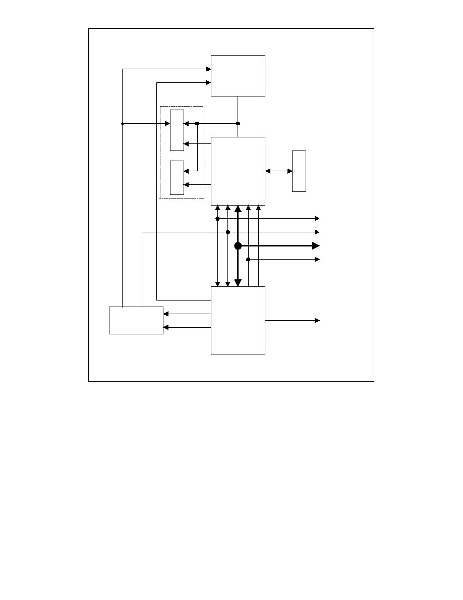
SMSC DS SLC90E66
Page 195
Rev. 07/10/2002
CPU
NORTH
BRIDGE
SLC90E66
SOUTH
BRIDGE
D
R
A
M
Clock
Generator
S
R
A
M
T
A
G
nCPU_STP
nPCI_STP
nSUS[A]
nSUS_STATI
nSUSCLK
nPCICLK
PCI Bus
nCLKRUN
nSTPCLK & nSLP
HCLK
HCLK
L2 Cache
Main
Memory
FIGURE 6 - SLC90E66 SYSTEM CONFIGURATION

SMSC DS SLC90E66
Page 196
Rev. 07/10/2002
11.1.1 HOST CLOCK CONTROL
The SLC90E66 supports four primary Host Clock Control Mechanisms with three types of variations. The SLC90E66
monitors system events to break out of clock control modes or to generate burst execution. Software can enable
clock control by setting the CC_EN bit with other optional control bits. Table 33 shows the bit settings required to
place the SLC90E66 in various modes of operation. The four primary mechanisms and three variations are:
§
Primary Host Clock Control Mechanisms
- Stop
Grant
-
Stop Clock
-
Sleep (Pentium II only)
-
Deep Sleep (Pentium II only)
§
Clock Control Variations
§
Manual
Throttle
§
Thermal
Throttle
§
Stop Break and Burst Execution
Table 33 - Programming of Clock Control Mechanisms
CLOCK CONTROL
MECHANISM
INVOKING
MECHANISM
CONTROL
BIT
CC_EN
CONTROL
BIT
STP_CLK_EN
CONTROL
BIT
SLEEP_EN
CONTROL
BIT
THT_EN
Thermal Throttle
External thermal
input: nTHRM
X
X
X
X
Disable Clock Control
0
X
X
X
Stop Grant/Quick Start
without Throttle
Read LVL2
Register
1
X
X
0
Stop Grant/Quick Start
with Throttle
None Required
1
X
X
1
Stop Grant/Quick Start
without Throttle,
Throttling begins upon
Stop Break Event
Read LVL2
Register
1
X
X
1
Reserved
Read LVL3
1
0
0
X
Sleep
Read LVL3
1
0
1
X
Stop Clock
Read LVL3
1
1
0
X
Deep Sleep
Read LVL3
1
1
1
X
Enable Burst Execution
(1)
Read LVL3
1
x
x
X
Note:
Burst Execution is always enabled for any of the above modes (except disabled and thermal throttle) if
BRST_EN bit is set.
Stop Grant State: The Stop Grant state can be initiated by a read to the LVL2 register when the CC_EN bit is
set.When initiated, the nSTPCLK signal is asserted and the SLC90E66 waits for the processor to issue a Stop Grant
bus cycle. Upon termination of the Stop Grant cycle, the SLC90E66 will assert the ZZ pin to the L2 SRAM if the
ZZ_EN bit is set. The SLC90E66 does not assert the nCPU_STP signal and the Host Clocks remain running in this
state. In this state, the processor disables clocks to portion of its internal logic, but is able to snoop host bus cycles in
order to maintain cache coherency. To exit this state, the SLC90E66 will first deassert the ZZ signal (if applicable)
and then deassert nSTPCLK.
Stop Clock State (Pentium II and Pentium III Processors only): The Stop Clock State is initiated by a read to the
LVL3 register. Once initiated, the SLC90E66 asserts the nSTPCLK signal and waits for the processor to issue a Stop
Grant Bus Cycle. Upon termination of the Stop Grant cycle, the SLC90E66 asserts the ZZ pin to L2 SRAM (if the
ZZ_EN is set), asserts the nSUS_STAT1 signal to Host Bridge to enable Suspend Refresh for the DRAM, and then
asserts the nCPU_STP signal to the clock synthesizer. The Host clocks stop running in this state. The processor
does not snoop host bus cycles and no other master devices should access main memory during this state. To exit
this state, the SLC90E66 will negate the nCPU_STP signal. At this time the SLC90E66 will first load the Fast Burst

SMSC DS SLC90E66
Page 197
Rev. 07/10/2002
Timer with the CPU_LCK value and count down allowing time for the processor PLL to lock. After the timer expires,
the SLC90E66 will negate the nSUS_STAT1 signal, the ZZ signal (if applicable), and finally nSTPCLK.
Sleep State (Pentium II and Pentium III processors only): The Sleep State is initiated by a read to the LVL3
register. Once initiated, the nSTPCLK signal is asserted and the SLC90E66 waits for the processor to issue a Stop
Grant bus cycle. When the Stop Grant cycle is terminated, the SLC90E66 asserts the ZZ pin to the L2 SRAM if the
ZZ_EN bit is set and after 50 PCI clocks asserts the nSLP signal. The SLC90E66 does not assert the nCPU_STP
signal and the Host clocks remain running in this state. In this state, the processor disables clocks to portions of its
internal logic. The processor does not snoop host bus cycles and system designers must ensure that no host cycles
to main memory are executed by other system masters. To exit this state, the SLC90E66 negates the nSLP signal,
waits approximately 32
µ
s and then negates the ZZ signal (if applicable) Two PCI clocks later nSTPCLK is negated.
Deep Sleep State (Pentium II and Pentium III processors only): The Deep Sleep State is Initiated by a read to the
LVL3 register. Once initiated,the nSTPCLK signal is asserted and the SLC90E66 waits for the processor to issue a
Stop Grant Bus Cycle. When the Stop Grant cycle is terminated, SLC90E66 asserts the ZZ pin to the L2 SRAM if the
ZZ_EN bit is set, asserts the nSLP signal, asserts the nSUS_STAT1 signal to Host Bridge to enable Suspend
Refresh for the DRAM, and then asserts the nCPU_STP signal to the clock synthesizer. The Host clocks stop running
in this state. The processor does not snoop host bus cycles and system designers must ensure that no host cycles to
main memory are executed by other system masters. To exit this state, the SLC90E66 negates the nCPU_STP
signal. Again, the SLC90E66 loads the Fast Burst Timer with the CPU_LCK value and counts down allowing time for
the processor PLL to lock. After the timer expires, the SLC90E66 negates the nSUS_STAT1 signal, the nSLP signal,
the ZZ signal (if applicable), and nSTP_CLK. The nSLP signal must adhere to the timing relations described in
Section 11.3.3 Suspend and Resume Control Signaling.
Thermal Throttle Control Mechanism: When the nTHRM signal is asserted for greater than 2 seconds, it indicates a
Thermal Alert condition. When this condition occurs and the system is not in the Stop Clock, Sleep or Deep Sleep
states, the SLC90E66 will automatically start toggling the nSTPCLK signal and ZZ signal (if the ZZ_EN bit set) with a
period of 31
µ
s and a programmable duty cycle. The system will toggle between full-speed operation and the Stop
Grant state. The duty cycle can be set in 12.5% increments by programming the THRM_DTY bits in the Count B
(CNTB) register. The functionality of thermal throttling is independent of the THRM_EN bit, which is used to enable
events, via generation of nSMI/SCI signal, for other power management functions. The THRM_DTY field must be
programmed by the BIOS. This emulates a reduced frequency host clock, resulting in reduced power and thermal
requirements. When the nTHRM signal is deasserted, the system will return to the clock control mechanism
previously in use. The thermal throttle state is not affected by the CC_EN setting. If nTHRM is asserted for more than
2 seconds while the SLC90E66 is in the Stop Grant state, the SLC90E66 will enter the thermal override state and
begin throttling nSTOPCLK as described above, thus overriding the manual throttling settings. If nTHRM is asserted
for more than 2 seconds while the SLC90E66 is in a Stop Clock state, the SLC90E66 will not enter the thermal
override state unless a break event occur.
If the nTHRM input pin is asserted for more than 2 seconds while the
SLC90E66 is in a Stop Grant, Stop Clock, Sleep, or Deep Sleep state, response to break events will occur
immediately and will not be deferred until after the nTHRM pin goes inactive. To prevent the case of being unable to
break out of the thermal override condition when break events are disabled, the Thermal Break Enable function
(enabled through the THRM_BK_EN bit, bit 2 of the GLBEN register) is implemented to optionally offer a break event
when nTHRM is deasserted after throttling from the thermal override. The state that the SLC90E66 transitions to
once nTHRM is deasserted depends on the state of the THRM_BK_EN bit (bit 2 of the GLBEN register). If
THRM_BK_EN=1, the SLC90E66 will break out of all clock control states and return to the C0 state. If
THRM_BK_EN=0, the SLC90E66 will return to the previous clock control state.
Clock Throttle Control Mechanism: I both the CC_EN bit and the THT_EN bit are set, the SLC90E66 will toggle
both nSTPCLK and ZZ (if ZZ_EN set) with a period of 31
µ
s (approximately 1024 33Mhz clock periods) and a
programmable duty cycle. Reads of the LVL2 register are not necessary to enter this state. The system will toggle
between full-speed operation and the Stop Grant state. The duty cycle can be set in 12.5% increments by
programming the THTL_DTY bits in the Processor Control P_CNTRL register. This emulates a reduced frequency
host clock, resulting in reduced power and thermal requirements. LVL2 register reads while in this state will do not
have any effect on the clock throttling.
Burst Execution and Stop Break Control Mechanism: Once the hardware has been placed into a clock control
state, it can be restored to full operation through a hardware event or software. Software can restore the system to
full speed operation by clearing the CC_EN bit, however, this is only possible after the system is woken up by a
resume event or if the system is in Stop Grant Throttle mode. Hardware events can be enabled to return the system
to a non-clock controlled condition. If the BRST_EN bit is cleared, these events are called Stop Break Events. If the
BRST_EN bit is set, these events are called Burst Events.
With the exception of the clock throttle controlled state where CC_EN and THT_EN are set, Stop Break events return
the system to a non-clock controlled state. In order to restore clock control, software must set up the desired clock
control configuration and again perform a read from LVL2 or LVL3 register to initiate the control. Break events have
no effect on the clock throttling when CC_EN and THT_EN are set.

SMSC DS SLC90E66
Page 198
Rev. 07/10/2002
Burst Events cause the reload of a Burst Timer, which begins to count down from its loaded initial value. While the
timer is counting, the system returns to full clock operation. Once the burst timer expires, the system automatically
returns to the clock controlled state. The SLC90E66 provides 2 different burst timers, a fast burst timer (which
generates a short burst period) and a slow burst timer (which generates a longer burst period). If burst events are
disabled during a burst, the SLC90E66 will enter the clock controlled state after the burst timer expires and will not be
able to break out. Burst events do not effect manual clock throttling (CC_EN and THT_EN are set). Burst events that
occur after the Burst Enable bit (BST_EN) has been set and before the LVL2 or LVL3 register read may cause the
LVL2 or LVL3 read to be missed. When this condition occurs, the system will not transition into the Level 2 or Level 3
clock control condition as intended but will remain at full speed. Software must ensure that no external burst events
are active when placing the system into a LVL2 or LVL3 state. To ensure this, prior to LVL2 or LVL3 register read,
only the Device 3 idle timer should be enabled as a burst event. The device 3 idle timer is then enabled with all
reload events disabled. The LVL2 or LVL3 register read is performed, placing the system into a LVL2 or LVL3 clock
control condition. The Device 3 idle timer will then generate a burst event upon expiration. During this first burst, the
desired burst events are then enabled. The system then functions as expected.
Stop Break events are a superset of fast burst and slow burst Events. If the BRST_EN bit is set, the burst events will
reload their associated burst timer. When the BRST_EN bit is cleared, these events will generate a Stop Break event.
Clock control mechanisms without and with burst enabled are shown in and respectively. The Fast Burst and Slow
Burst timers and the burst event programming information are summarized as follows.
Note that the shortest time that the SLC90E66 deasserts nSTPCLK is 3.9
µ
s (87.5% duty cycle at 32.2 KHz).
Because short deasertions (<1
µ
s) can be missed by the CPU, transitions in and out of clock control modes must be
performed such that the 2.9
µ
s minimum CPU nSTPCLK deassertion specification is not exceeded.
FAST BURST TIMER PROGRAMMING INFORMATION:
Resolution: 1msecond
Count:
5-bit field
[FB_CNT]
SLOW BURST TIMER PROGRAMMING INFORMATION:
Resolution:
1 second
Count:
4-bit field
[SB_CNT]
FAST BURST TIMER PROGRAMMING INFORMATION (FOR CPU PLL LOCK):
Resolution: 1
µ
sec or 1 msec
[CPU_SEL]:
Count: 5-bit field
[CPU_LCK]
FAST BURST EVENTS
Event Name
Control Bit
IRQ0
[BRLD_EN_IRQ0]
IRQ8
[BRLD_EN_IRQ8]
NMI, INIT, IRQ[1, 3-7, 9-15]
[BRLD_EN_IRQ]
PCI Bus Master Activity
[BRLD_EN_BM]
Device 0-13 Monitors:
[BRLD_EN_DEVx] x=1 - 13
Slow/Fast Burst Select
[BRLD_SEL_DEVx] x=1 - 3, 5
Power Management Events
[BRLD_EN_PME]
PCI Activity (nFRAME Assertion):
[BRLD_EN_PCI]
GPI1 Asserted:
[BRLD_EN_PME]
LID Asserted:
[BRLD_EN_PME]
- Polarity Select:
[LID_POL]
PWRBTN Asserted:
[BRLD_EN_PME]
nSMI Event:
[BRLD_EN_PME]
SLOW BURST EVENTS
Event Name
Control Bit
Device 0 - 13 Monitors:
[BRLD_EN_DEVx] x = 1 - 3, 5
Slow/Fast Burst Select
[BRLD_SEL_DEVx] x = 1 - 3, 5

SMSC DS SLC90E66
Page 199
Rev. 07/10/2002
FIGURE 7 - CLOCK CONTROL MECHANISMS (NON-BURST ENABLE)
Clocks
nSTPCLK
CC_EN=1 and
THT_EN=1
CC_EN=0 or
THT_EN=0
CC_EN=1 and
THT_EN=1
THROTTLE MODE
Clocks Running
Clocks Running
Read LVL2 by
OS or APM
Stop Break
Event
Read LVL2 by
OS or APM
Clocks
nSTPCLK
STOP GRANT MODE
Clocks Stopped
Clocks
nSTPCLK
STOP CLOCK
Read LVL2 by
OS or APM
Stop Break
Event
Read LVL2 by
OS or APM
Normal
Working
State
Clocks Stopped
Clocks Running
Clocks Running
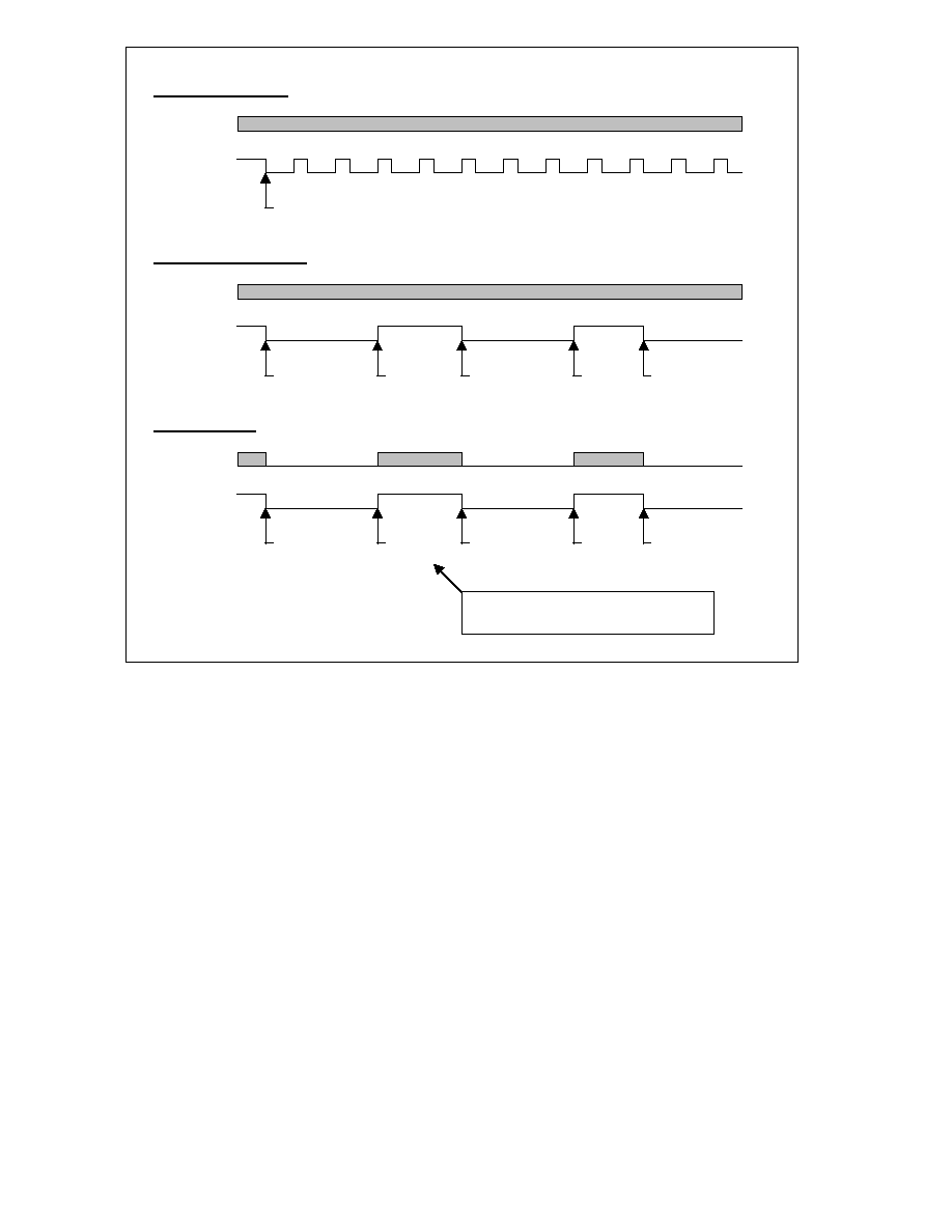
SMSC DS SLC90E66
Page 200
Rev. 07/10/2002
FIGURE 8 - CLOCK CONTROL MECHANISMS (BURST ENABLED)
11.1.2 STOP CLOCK STATE EXAMPLE SEQUENCE
The Stop Clock Mode requires special consideration to allow the processor PLL to stabilize before starting any
activity that would involve the processor. The following is an example of system transition into and out of Stop Clock.
FIGURE 9 shows an example timing diagram. An example of the transition into and out of Stop clock is as follows:
To Enter Stop Clock State
Initialization
§
Software configures the SLC90E66 for the appropriate Clock Control Mechanism.
§
Software disables the PCI arbiter in the Host Bridge.
Invoke State Transition
§
Software reads register LVL3 to enable the Stop Clock Mode.
SLC90E66 Actions (In Sequence)
§
SLC90E66
asserts
nSTPCLK.
§
The processor accepts nSTPCLK, flushes buffers, issues STOP GRANT cycles.
§
The North Bridge forwards Stop Grant bus cycle to the PCI bus then does a PCI Master Abort cycle.
§
The North Bridge completes the CPU by returning a nBRDY to the processor.
§
The processor gates the internal clocks to the processor core and enters the Stop Grant state.
§
The
SLC90E66 asserts ZZ pin to L2 SRAM if the ZZ_EN bit is set.
Clocks Running
CC_EN=1 and
THT_EN=1
Clocks Running
Read LVL2 by
OS or APM
Slow
Burst
Event
Slow Burst
Timer
Expires
Fast
Burst
Event
Fast Burst
Timer
Expires
Read LVL2 by
OS or APM
Slow
Burst
Event
Slow Burst
Timer
Expires
Fast
Burst
Event
Fast Burst
Timer
Expires
Clocks Stopped
The Clock Control Unit remains in the
Enabled mode until Software breaks it out
Clocks
nSTPCLK
THROTTLE MODE
Clocks
nSTPCLK
STOP GRANT MODE
Clocks
nSTPCLK
STOP CLOCK
Clocks Stopped
Clocks Stopped

SMSC DS SLC90E66
Page 201
Rev. 07/10/2002
§
SLC90E66 waits up to two 32Khz clock periods after receiving the Stop Grant Bus Cycle to assert nSUS_STAT1
to the North Bridge. The North Bridge must complete pending DRAM cycle before the nSUS_STAT1 is asserted.
§
The North Bridge switches from Normal Refresh to Suspend Refresh with the assertion of nSUS_STAT1.
§
The SLC90E66 waits an additional 32Khz clock period after the assertion of nSUS_STAT1 to allow the North
bridge to switch refresh modes and then asserts nCPU_STP to the Clock Synthesizer.
§
The Clock Synthesizer stops the host clocks to the Processor Complex, including L2 cache, North Bridge and
SDRAM.
§
The processor now is in Stop Clock state.
§
SLC90E66 waits for Stop Break or Burst Event to occur.
To Leave the Stop Clock State
Invoke State Transition
§
A Stop Break or Burst Event occurs.
SLC90E66 Actions (In Sequence)
§
The SLC90E66 negates nCPU_STP to the Clock Synthesizer to start the host clocks.
§
The SLC90E66 loads the Fast Burst Timer with the [CPU_LCK] value and then counts down to wait for the
processor PLL to start and lock.
§
The SLC90E66 deasserts nSUS_STAT1 after the Fast Burst Timer expires.
§
The North Bridge switches from Suspend Refresh to Normal Refresh after the negation of nSUS_STAT1.
§
The SLC90E66 waits up to two 32Khz clock periods after the negation of nSUS_STAT1 and then negates
nSTPCLK. The SLC90E66 negates ZZ at least 2 PCI clocks before the deassertion of nSTPCLK.
Result of the SLC90E66 Operation
§
The
processor returns to the On state and resumes normal operation.
§
The North Bridge PCI Arbiter still remains in disabled state. Bus Master requests must be trapped to generate
nSMI, which will invoke power management software to enable the PCI Arbiter. The Device 8 Peripheral Device
Monitor can be used for that purpose.
HCLK
nSTPCLK
ZZ
nnSUS_STAT1
nCPU_STP
PCI BUS
1
2
3
4
Request to
CLKRUN
Stop Grant
Cycle
5
FIGURE 9 - STOP CLOCK EXAMPLE
(See notes below for description of numbered items)
Notes:
1) The SLC90E66 waits two 32kHz clock periods to assert nSUS_STAT1 to the Host Bridge to allow
the Host Bridge to complete pending cycles to DRAM.
2) The SLC90E66 waits one 32 kHz clock period to assert nCPU_STP to the Clock Synthesizer to
allow the Host Bridge to switches from Normal Refresh to Suspend Refresh. The assertion of
nCPU_STP will stop the Host Clocks to the processor, host bridge, L2 Cache, and SDRAM.
3) The SLC90E66 waits for the processor PLL to start and lock (about CPU_LCK time + one 32KHz
period) then deasserts the nSUS_STAT1 signal.
4) The SLC90E66 waits 2-3 32KHz periods if SLEEP_EN = 0, or 3-5 32KHz periods if SLEEP_EN = 1
and then deasserts the nSTPCLK signal.
5) The SLC90E66 deasserts ZZ at least 2 PCI clocks before the deassertion of nSTPCLK.

SMSC DS SLC90E66
Page 202
Rev. 07/10/2002
11.1.3 PCI CLOCK CONTROL
The SLC90E66 follows the nCLKRUN protocol as specified by the PCI Mobile Design Guide to manage the PCI
Clock. The SLC90E66 is the Central Resource of the nCLKRUN protocol.
If the CLKRUN_EN bit is set in the Processor Control Register, the SLC90E66 will issua a request to stop the PCI
clock if the bus has been idle for 26 PCI clocks. The SLC90E66 will drive the PCI nCLKRUN signal high for four
clocks. If no other device in the system denies the request to stop before the 5
th
PCI clock, the SLC90E66 will assert
nPCI_STP signal to the Clock Synthesizer to gate the PCI clocks to the system.
The SLC90E66 should always receive a PCI clock even after the clocks have been stopped to the rest of the system.
The clock synthesizer must have one non-gated PCI clock signal routed to the SLC90E66. The clock synthesizer
must follow the following timing diagrams shown in FIGURE 10 and FIGURE 11 for stopping and starting the PCI
clocks.
FIGURE 10 - PCI CLOCK STOP TIMING
FIGURE 11 PCI CLOCK START TIMING
nPCI_CLK
SLC90E66
PCICLK
System
PCICLK
nPCI_CLK
SLC90E66
PCICLK
System
PCICLK
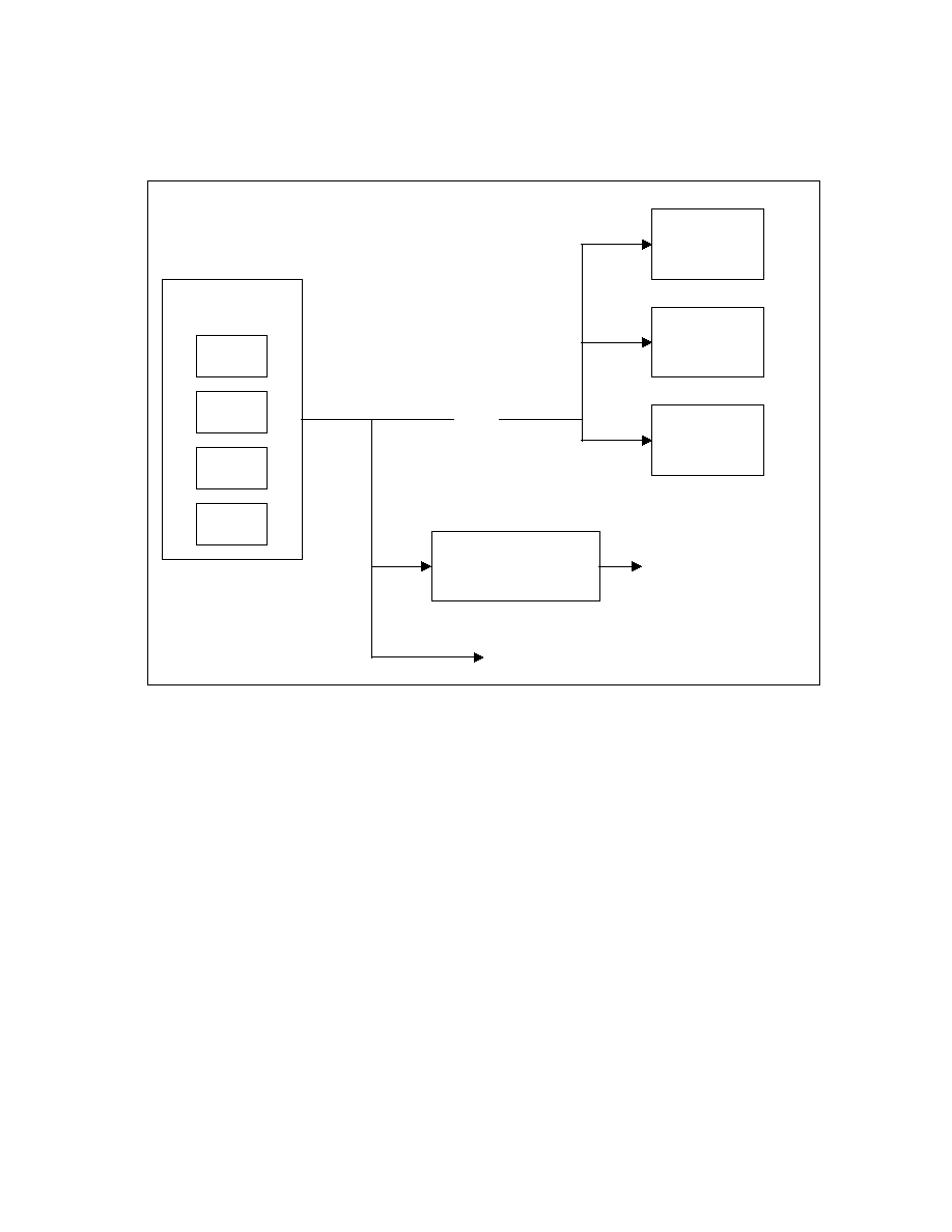
SMSC DS SLC90E66
Page 203
Rev. 07/10/2002
11.2 Peripheral Device Management
The Peripheral Device Management mechanisms provide means to detect idle peripheral devices and to trap
accesses to peripheral devices that have been powered-down. Enabled device activities can also reload the Global
Standby Timer or can generate a Burst or Stop Break event. Device accesses, either I/O or Memory, are monitored
from the PCI bus. There are 14 independent device monitors, each capable of detecting activity for a different type of
device. FIGURE 12 shows the logic associated with each device monitor.
FIGURE 12 - PERIPHERAL DEVICE MANAGEMENT
11.2.1 DEVICE MONITOR AND IDLE TIMER
Each device (except Device 12 and 13) has an Idle Timer that can be reloaded by activity on that device. Activity
monitoring is specific to each device and can include the following:
§
Device Access. Specific I/O or memory ranges associated with that device are monitored on the PCI bus. Many
devices have multiple options to set up a wide range of system configurations.
§
DMA Acknowledge. nDACK is used for DMA transfers by the device, such as Audio, Floppy, and LPT.
§
General Purpose Input. Most device monitors can watch for assertion of a specific General Purpose Input
(GPI) pin. Each GPI signal can have its assertion polarity modified to be high or low. Two GPI signals (device 12
and 13) can also be enabled for edge transition detection.
§
System Activity. Miscellaneous activity, such as Keyboard or Mouse interrupt, PCI bus Master activity, or PCI
bus utilization (such as nFRAME assertion) may be monitored for specific device.
A device event can be enabled to reload the device's Idle Timer as well as to reload the Global Standby Timer or the
Fast or Slow Burst Timers.
I/O
Memory
nDACK
Bus
REQ
GPI
Device Access
Global
Standby
Timer
Device
Idle Timer
Clock Break/
Burst Timer
I/O Trap
(for each device in
Power Saving Mode)
Reload
Forward Cycle to EIO Bus
nSMI,
I/O-Restart
[Trap-Status]

SMSC DS SLC90E66
Page 204
Rev. 07/10/2002
Some of the monitors can serve multiple functions. For example, the Device 3 IDE secondary IDE Drive 1 monitor
can also be enabled as a programmable Software Timer. The Device 8 LPT monitor can be enabled to monitor
parallel port activity or PCI Bus Master activity.
When the Idle Timer expires due to no detected activity, an Idle Status bit is set and an nSMI is generated if enabled.
The power management software can then put the device into a power managed state. The idle timers stop counting
when the SM_FREEZE bit is set. This can be used to keep the idle timers from counting down when the system is
executing an SMI routine.
11.2.2 DEVICE
TRAP
Each device monitor can enable an IO Trap so that when software makes an access to the enabled I/O or memory
range a trap status bit is set and an nSMI is generated if enabled. The device trap feature normally is enabled for
devices which have been switched to a power down state so that when the power-down device's address ranges are
decoded software can be invoked (via nSMI) to restore the device to normal working state.
The I/O Trap nSMI is synchronous to the completion of the I/O instruction. The I/O instruction is completed when
nBRDY is returned to the processor. SLC90E66 will coordinate the assertion of nSMI to the processor with the
generation of nBRDY to the processor form the Host Bridge chip such that nSMI is asserted at least 3 HCLKs before
nBRDY is asserted. This will allow the processor to perform an I/O restart cycle.
If the device to be trapped is a PCI device, the SLC90E66 must be enabled to claim the cycle so that nSMI can be
generated synchronously. The SLC90E66 should be programmed to send the I/O access cycle to the ISA bus where
it will be terminated normally (the read cycle will return unknown data).
11.2.3 PERIPHERAL DEVICE MANAGEMENT
Following is a brief description of the power management process for peripheral devices:
§
Initialization. The power management software initializes the device's I/O address range and the Idle Timer
counter for each peripheral device.
§
Normal to Low Power State Transition. When power management software enables the Idle Timer for a
device, the Idle Timer starts to count down. Any detected activity of the enabled device will reload its Idle Timer.
When the Idle Timer expires, the associated idle status bit is set, and a nSMI is generated. The SMI handler can
identify the device from the idle status bit, then put the peripheral device into a low power state, disable the Idle
Timer and enable the I/O Trap mechanism for the device.
§
Low Power to Normal State Transition. When the system performs an access to an I/O Trap enabled device
range, the access is trapped, a nSMI is generated, and the corresponding I/O Trap SMI status bit is set. The SMI
handler can identify the device by examining the I/O Trap SMI status bits, restore the peripheral device to "on"
state, clear the Trap SMI status bits, and enable the Idle Timer hardware. The processor will then issue an I/O
restart to access the device again.
11.2.4 PCI/ISA PERIPHERAL DEVICES
The Device Activity Monitor is watching cycles on the PCI bus to generate activity events. The device monitors also
can be enabled to forward cycles that address the device's enabled address ranges to the ISA bus. Devices that
reside on the ISA bus must have both address ranges selected and enabled and the ISA/EIO forwarding enabled.
Table 34 summarizes peripheral devices that are monitored by the SLC90E66 Power Management function.

SMSC DS SLC90E66
Page 205
Rev. 07/10/2002
Table 34 - Peripheral Device Overview
MONITORED DEVICE ACTIVITIES
TIMERS AFFECTED
PERIPHERAL
DEVICE
ADDRESS
RANGES
nDACK
GPI
IDLE
TIMER
GLOBAL
STANDBY
FAST
BURST
SLOW
BURST
0. Primary IDE
Drive 0
1F0h - 1F7h
3F6h
IDE
nPDDACK
CNT-A
X
X
1. Primary IDE
Drive 1
1F0h-1F7h
3F6h
IDE
nPDDACK
GPI5
CNT-A
X
X
X
2. Secondary IDE
Drive 0
170h - 177h
376h
IDE
nSDDACK
GPI6
CNT-A
X
X
X
3. Secondary IDE
Drive 1 / Software
SMI Timer
170h - 177h
376h
IDE
nSDDACK
GPI0
SWCNT
X
X
X
4. Audio
300h-303h MIDI
310h-313h MIDI
320h-323h MIDI
330h-333h MIDI
200h-207h GAME
388h-38Bh ADLIB
220h-233h SB8/16
240h-253h SB8/16
260h-273h SB8/16
280h-293h SB8/16
530h-537h MSS
604h-60Bh MSS
E80h-E87h MSS
F40h-F47h MSS
any or all:
nDACK[x],
x=0,1,3,5,6,7
GPI13
CNT-B
X
X
5. FDD
3F0h-3F5h, 3F7h
370h-375h, 3F7h
nDACK2
GPI14
CNT-B
X
X
X
6. Serial Port A
(Modem)
3F8h-3FFh COM1
2F8h-2FFh COM2
3E8h-3EFh COM3
2E8h-2EFh COM4
220h-227h
228h-22Fh
238h-23Fh
338h-33Fh
GPI15
CNT-B
X
X
7. Serial Port B
(IR)
3F8h-3FFh COM1
2F8h-2FFh COM2
3E8h-3EFh COM3
2E8h-2EFh COM4
220h-227h
228h-22Fh
238h-23Fh
338h-33Fh
GPI16
CNT-B
X
X

SMSC DS SLC90E66
Page 206
Rev. 07/10/2002
MONITORED DEVICE ACTIVITIES
TIMERS AFFECTED
PERIPHERAL
DEVICE
ADDRESS
RANGES
nDACK
GPI
IDLE
TIMER
GLOBAL
STANDBY
FAST
BURST
SLOW
BURST
8A. LPT
LPT_DEC_SEL:
0,0=3BCh-3BFh,
7BCh-7BEh
0,1=378h-37Fh,
778h-77Ah
1,0=278h-27Fh,
678h-67Ah
one of:
nDACK[x]
x=0,1,3
GPI17
BM_CN
T
X
X
8B. Bus Master
Activity
nPCIREQ
[A-D],
nPHOLD
Dev8
Timer
X
X
9. Generic I/O
Range 0
16-byte I/O range
GPI4
CNT-C
X
X
10. Generic I/O
Range 1
16-byte I/O range
GPI18
CNT-C
X
X
User Interface:
Graphics,
Keyboard, Mouse,
PCI Utilization
1M to 8M Mem
range.
A0000h-BFFFFh,
3B0h-3DFh VGA,
60h, 64h, IRQ0,
IRQ12/M
GPI19
CNT-D
X
X
12.
Cardbus 0
16-byte I/O range,
32K-4M Mem
range
GPI20
X
X
13.
Cardbus 1
16-byte I/O range,
32K-4M Mem
range
GPI21
X
X
11.2.5 DEVICE SPECIFIC
DETAILS
This section provides detailed descriptions for the 14 device monitors. For each device monitor, the system events
that can cause actions such as timer reloads or IO traps are listed. The names of register bits that are programmed
to enable power management resources or status bits set when events occur are shown in brackets for each device.
11.2.5.1 Device 0: IDE Primary Drive 0
Device 0 monitors the primary IDE device, drive 0. The IDE device DRV bit (bit 4 of port 1F6h) is shadowed to
determine if drive 0 is active on the primary connector.
Device 0 System Events
§
PCI accesses to IO address 1F0h-1F7h, 3F6h, independent of whether IDE is enabled in PCI function 1, if IDE
drive 0 is set. This allows monitoring of devices on PCI or ISA bus. This can cause idle, burst, or global standby
timer reloads or I/O trap nSMI assertion
§
nPDDACK assertion if primary IDE drive 0 is active and BMIDE is active for primary connector. This can cause
idle, burst, or global standby timer reloads.
§
No GPI events are associated with device 0.

SMSC DS SLC90E66
Page 207
Rev. 07/10/2002
Device 0 Idle Timer
§
Resolution: 1 or 8 second
Control Bit: [IDL_SEL_DEV0]
§
Timer count: 4 bit
Register Bit: [IDL_CNTA]
§
Enable:
Control Bit: [IDL_EN_DEV0]
§
Expiration nSMI Assertion
Control Bit: IDL_EN_DEV0]
Status Bit: [IDL_STS_DEV0]
Global Standby Timer Reload:
§
Enable:
Control Bit: [GRLD_EN_DEV0]
Burst Timer Reload (Slow burst)
§
Enable:
Control Bit: [BRLD_EN_DEV0]
I/O Trap nSMI:
§
Enable:
Control Bit: [TRP_EN_DEV0]
Status Bit:[TRP_STS_DEV0]
11.2.5.2 Device 1: IDE Primary Drive 1
Device 1 monitors the primary IDE device, drive 1 and GPI5. The IDE device DRV bit (bit 4 of port 1F6h) is shadowed
to determine if drive 1 is active on the primary connector.
Device 1 System Events
§
PCI accesses to IO address 1F0h-1F7h, 3F6h, independent of whether IDE is enabled in PCI function 1, if IDE
drive 1 is active. This allows monitoring of devices on PCI or ISA bus. This can cause idle, burst, or global
standby timer reloads or IO trap nSMI assertion.
§
nPDDACK assertion if the primary IDE drive 1 is active, the IDE interface is configured as primary and secondary
and BMIDE is active for the primary connector. This can cause idle, burst, or global standby timer reloads.
§
Assertion of GPI5. The polarity of the active signal level (high or low) is selectable. This can cause idle, burst, or
global standby timer reloads or IO Trap nSMI assertion.
Device 1 GPI5 Enable:
§
Enable:
Control Bit: [GPI_EN_DEV1]
§
Polarity
Selection
Control Bit: [GPI_POL_DEV1]
Device 1 Idle Timer:
§
Resolution: 1 or 8 second
Control Bit: [IDL_SEL_DEV1]
§
Timer count: 4 bit
Register Bit: [IDL_CNTA]
§
Enable/Reload:
Control Bit: [IDL_EN_DEV1]
§
Expiration nSMI Assertion
Control Bit: [IDL_EN_DEV1]
Status Bit: [IDL_STS_DEV1]

SMSC DS SLC90E66
Page 208
Rev. 07/10/2002
Global Standby Timer Reload:
§
Enable:
Control Bit: [GRLD_EN_DEV1]
Burst Timer Reload:
§
Enable:
Control Bit: [BRLD_EN_DEV1]
§
Fast or Slow Burst Select
Control Bit: [BRLD_SEL_DEV1]
IO Trap nSMI:
§
Enable
Control Bit: [TRP_EN_DEV1]
Status Bit: [TRP_STS_DEV1]
11.2.5.3 Device 2: IDE Secondary Drive 0
Device 2 monitors the Secondary IDE device, drive 0 and GPI6. The IDE device DRV bit (bit 4 of port 176h) is
shadowed to determine if drive 0 is active on the secondary connector.
Device 2 System Events
§
PCI accesses to IO address 170h-177h, 376h, independent of whether IDE is enabled in PCI function 1, if the
secondary IDE drive 0 is active. This allows monitoring of devices on PCI or ISA bus. This can cause idle, burst,
or global standby timer reloads or IO trap nSMI assertion
§
nSDDACK assertion if the secondary IDE drive 0 is active, the IDE interface is configured as primary and
secondary and BMIDE is active for the secondary connector. This can cause idle, burst, or global standby timer
reloads.
Assertion of GPI6. The polarity of the active signal level (high or low) is selectable. This can cause idle, burst, or
global standby timer reloads or IO Trap nSMI assertion.
Device 2 GPI6 Enable:
§
Enable:
Control Bit: [GPI_EN_DEV2]
§
Polarity
Selection
Control Bit: [GPI_POL_DEV2]
Device 2 Idle Timer:
§
Resolution: 1 or 8 second
Control Bit: [IDL_SEL_DEV2]
§
Timer count: 4 bit
Register Bit: [IDL_CNTA]
§
Enable/Reload:
Control Bit: [IDL_EN_DEV2]
§
Expiration nSMI Assertion
Control Bit: [IDL_EN_DEV2]
Status Bit: [IDL_STS_DEV2]
Global Standby Timer Reload:
§
Enable:
Control Bit: [GRLD_EN_DEV2]
Burst Timer Reload:
§
Enable:
Control Bit: [BRLD_EN_DEV2]
§
Fast or Slow Burst Select
Control Bit: [BRLD_SEL_DEV2]

SMSC DS SLC90E66
Page 209
Rev. 07/10/2002
IO Trap nSMI:
§
Enable:
Control Bit: [TRP_EN_DEV2]
Status Bit: TRP_STS_DEV2]
11.2.5.4 Device 3: IDE Secondary Drive 1
Device 3 monitors the Secondary IDE device, drive 1 and GPI0. The IDE device DRV bit (bit 4 of port 176h) is
shadowed to determine if drive 1 is active on the secondary connector. Device 3 can also be used as a Software
nSMI Timer. It has a configuration bit to disable the Idle Timer Reload so that the timer can be allowed to expire
based only on the timer count.
Device 3 System Events
§
PCI accesses to IO address 170h-177h, 376h, independent of whether IDE is enabled in PCI function 1, if the
secondary IDE drive 1 is active. This allows monitoring of devices on the PCI or ISA bus. This can cause idle,
burst, or global standby timer reloads or IO trap nSMI assertion.
§
nSDDACK assertion if the secondary IDE drive 1 is active, the IDE interface is configured as primary and
secondary and BMIDE is active for the secondary connector. This can cause idle, burst, or global standby timer
reloads.
§
Assertion of GPI0. The polarity of the active signal level (high or low) is selectable. This can cause idle, burst, or
global standby timer reloads or IO Trap nSMI assertion.
Device 3 GPI0 Enable:
§
Enable:
Control Bit: [GPI_EN_DEV3]
§
Polarity
Selection
Control Bit: [GPI_POL_DEV3]
Device 3 Idle Timer:
§
Resolution: 1 ms or 8 second
Control Bit: [IDL_SEL_DEV3]
§
Timer count: 4 bit
Register Bit: [SW_CNT]
§
Enable/Reload:
Control Bit: [IDL_EN_DEV3]
§
Reload Disable (to select SW func.):
Control Bit: [IDL_RLD_EN_DEV3]
§
Expiration nSMI Assertion
Control Bit: [IDL_EN_DEV3]
Status Bit: [IDL_STS_DEV3]
Global Standby Timer Reload:
§
Enable:
Control Bit: [GRLD_EN_DEV3]
Burst Timer Reload:
§
Enable:
Control Bit: [BRLD_EN_DEV3]
§
Fast or Slow Burst Select
Control Bit: [BRLD_SEL_DEV3]
I/O Trap nSMI:
§
Enable:
Control Bit: [TRP_EN_DEV3]
Status Bit: [TRP_STS_DEV3]

SMSC DS SLC90E66
Page 210
Rev. 07/10/2002
11.2.5.5 Device
4:
Audio
Device 4 monitors an audio subsystem and GPI13. The available address ranges cover the following type of audio
devices: 8/16 bit Sound Blaster, standard Game Port, ADLIB music synthesizer, Microsoft Sound System, and MIDI.
The actual address ranges selectable for each type is shown below.
Device 4 System Events
§
PCI accesses to any of the enabled IO addresses. This can cause idle, burst, or global standby timer reloads, IO
trap nSMI assertion, or forward the cycle from PCI to ISA.
§
nDACKx assertion (x=0,1,3,5,6,7) if enabled. This can cause idle, burst, or global standby timer reloads.
§
Assertion of GPI13. The polarity of the active signal level (high or low) is selectable. This can cause idle, burst,
or global standby timer reloads.
Device 4 GPI13 Enable:
§
Enable:
Control Bit: [GPI_EN_DEV4]
§
Polarity
Selection
Control Bit: [GPI_POL_DEV4]
Device 4 Address Ranges:
§
Sound
Blaster
Control Bit: [SB_EN]
Selection Bits: [SB_SEL]
220h-22Fh, 230h-233h, OR
240h-24Fh, 250h-253h, OR
260h-26Fh, 270h-273h, OR
280h-28Fh, 290h-293h
§
Game
Port
Control Bit: [SB_EN]
200h-207h
§
ADLIB
Synthesizer
Control Bit: [SB_EN]
388h-38Bh
Microsoft Sound System:
§
Control Bit: [MSS_EN]
Selection Bits: [MSS_SEL]
530h-537h OR
604h-60Bh OR
E80h-E87h OR
F40h-F47h
§
MIDI
Control Bit: [MIDI_EN]
Selection Bits: [MIDI_SEL]
300h-303h OR
310h-313h OR
320h-323h OR
330h-333h

SMSC DS SLC90E66
Page 211
Rev. 07/10/2002
Device 4 ISA Forwarding Enable:
§
MIDI
Control Bit: [MIDI_EIO_EN]
§
MSS
Control Bit: [MSS_EIO_EN]
§
Game
Control Bit: [GAME_EIO_EN]
§
Sound
Blaster
Control Bit: [SB_EIO_EN]
Device 4 nDACKx (x=0,1,3,5,6,7)
§
Enable:
Control Bit: [DACKx_EN_DEV4]
Device 4 Idle Timer:
§
Resolution:
1
second
§
Timer count: 5 bit
Register Bit: [IDL_CNTB]
§
Enable/Reload:
Control Bit: [IDL_EN_DEV4]
§
Expiration nSMI Assertion
Control Bit: [IDL_EN_DEV4]
Status Bit: [IDL_STS_DEV4]
Global Standby Timer Reload:
§
Enable:
Control Bit: [GRLD_EN_DEV4]
Burst Timer Reload (Fast Bursts Only):
§
Enable:
Control Bit: [BRLD_EN_DEV4]
I/O Trap nSMI:
§
Enable:
Control Bit: [TRP_EN_DEV4]
Status Bit: [TRP_STS_DEV4]
11.2.5.6 Device 5: Floppy Disk Drive
Device 5 monitors accesses to Floppy Drive Controller or GPI14.
Device 5 System Events
§
PCI accesses to IO addresses for the floppy drive, selectable below. This can cause idle, burst, or global
standby timer reloads, IO trap nSMI assertion, or forwarding of the cycle from PCI to ISA.
§
nDACK2 assertion if enabled. This can cause idle, burst, or global standby timer reloads.
§
Assertion of GPI14. The polarity of the active signal leel (high or low) is selectable. This can cause idle, burst, or
global standby timer reloads.
Device 5 GPI14 Enable:
§
Enable:
Control Bit: [GPI_EN_DEV5]
§
Polarity
Selection
Control Bit: [GPI_POL_DEV5]
Device 5 Address Ranges:
§
Floppy
Drive:
Control Bit:
[FDC_MON_EN]
Selection Bits: [FDC_DEC_SEL]

SMSC DS SLC90E66
Page 212
Rev. 07/10/2002
3F0h-3F5h, 3F7h OR 370h-375h, 377h
Device 5 ISA Forwarding Enable:
Control Bit:
[EIO_EN_DEV5]
Device 5 nDACK2 Enable:
Control Bit:
[RES_EN_DEV5]
Device 5 Idle Timer:
§
Resolution:
1
second
§
Timer count: 5 bit
Register Bit: [IDL_CNTB]
§
Enable/Reload:
Control Bit: [IDL_EN_DEV5]
§
Expiration nSMI Assertion
Control Bit: [IDL_EN_DEV5]
Status Bit: [IDL_STS_DEV5]
Global Standby Timer Reload:
§
Enable:
Control Bit: [GRLD_EN_DEV5]
Burst Timer Reload:
§
Enable:
Control Bit: [BRLD_EN_DEV5]
§
Fast or Slow Burst Select
Selection Bit: [BRLD_SEL_DEV5]
I/O Trap nSMI:
§
Enable:
Control Bit: [TRP_EN_DEV5]
Status Bit: [TRP_STS_DEV5]
11.2.5.7 Device 6: Serial Port A
Device 6 monitors accesses to Serial Port A or GPI15. Device 7 also monitors serial port resources. This gives the
capability to monitor 2 separate serial ports in a system.
Device 6 System Events
§
PCI accesses to IO addresses for a serial port, selectable below. This can cause idle, burst, or global standby
timer reloads, I/O trap nSMI assertion, or forwarding of the cycle from PCI to ISA.
§
Assertion of GPI15. The polarity of the active signal level (high or low) is selectable. This can cause idle, burst, or
global standby timer reloads.
Device 6 GPI15 Enable:
§
Enable:
Control Bit: [GPI_EN_DEV6]
§
Polarity
Selection
Control Bit: [GPI_POL_DEV6]
Device 6 Address Ranges:
§
Serial Port A: Control Bit: [SA_MON_EN]
Selection Bit: [COMA_DEC_SEL]
3F8h-3FFh, or
2F8h-2FFh, or
220h-227h, or
228h-22Fh, or
238h-23Fh, or
2E8h-2EFh, or
338h-33Fh, or
3E8h-3Efh

SMSC DS SLC90E66
Page 213
Rev. 07/10/2002
Device 6 ISA Forwarding Enable:
Control Bit: [EIO_EN_DEV6]
Device 6 Idle Timer:
§
Resolution:
1
second
§
Timer count: 5 bit
Register Bit: [IDL_CNTB]
§
Enable/Reload:
Control Bit: [IDL_EN_DEV6]
§
Expiration nSMI Assertion
Control Bit: [IDL_EN_DEV6]
Status Bit: [IDL_STS_DEV6]
Global Standby Timer Reload:
§
Enable:
Control Bit: [GRLD_EN_DEV6]
Burst Timer Reload (Fast Burst Only):
§
Enable:
Control Bit: [BRLD_EN_DEV6]
IO Trap nSMI:
§
Enable:
Control Bit: [TRP_EN_DEV6]
Status Bit: [TRP_STS_DEV6]
11.2.5.8 Device 7: Serial Port B
Device 7 monitors accesses Serial Port B or GPI16. Device 7 also monitors serial port resources. This gives the
capability to monitor 2 separate serial ports in a system.
Device 7 System Events
§
PCI accesses to IO addresses for a serial port, selectable below. This can cause idle, burst, or global standby
timer reloads, I/O trap nSMI assertion, or forwarding of the cycle from PCI to ISA.
§
Assertion of GPI16. The polarity of the active signal level (high or low) is selectable. This can cause idle, burst,
or global standby timer reloads.
Device 7 GPI16 Enable:
§
Enable:
Control Bit: [GPI_EN_DEV7]
§
Polarity
Selection
Control Bit: [GPI_POL_DEV7]
Device 7 Address Ranges:
§
Serial Port B:
Control Bit:
[SA_MON_EN]
Selection Bits: COMB_DEC_SEL]
3F8h-3FFh, or
2F8h-2FFh, or
220h-227h, or
228h-22Fh, or
238h-23Fh, or
2E8h-2EFh, or
338h-33Fh, or
3E8h-3Efh

SMSC DS SLC90E66
Page 214
Rev. 07/10/2002
Device 7 ISA Forwarding Enable:
Control Bit:
[EIO_EN_DEV7]
Device 7 Idle Timer:
§
Resolution:
1
second
§
Timer count: 5 bit
Register Bit: [IDL_CNTB]
§
Enable/Reload:
Control Bit: [IDL_EN_DEV7]
§
Expiration nSMI Assertion
Control Bit: IDL_EN_DEV7]
Status Bit: [IDL_STS_DEV7]
Global Standby Timer Reload:
§
Enable:
Control Bit: [GRLD_EN_DEV7]
Burst Timer Reload (Fast Burst Only):
§
Enable:
Control Bit: [BRLD_EN_DEV7]
I/O Trap nSMI:
§
Enable:
Control Bit: [TRP_EN_DEV7]
Status Bit: [TRP_STS_DEV7]
11.2.5.9 Device 8: LPT (Parallel Port)
Device 8 monitors accesses to Parallel Port or GPI17. It can also be used to monitor PCI Bus Master activity.
Device 8 System Events
§
PCI accesses to IO addresses for a parallel port, selectable below. This can cause idle, burst, or global standby
timer reloads, I/O trap nSMI assertion, or forwarding of the cycle from PCI to ISA.
§
Assertion of GPI17. The polarity of the active signal level (high or low) is selectable. This can cause idle, burst,
or global standby timer reloads.
§
Assertion of nPCIREQ[A-D] or nPHOLD, signifying PCI Master activity. This can cause idle, burst, or global
standby timer reloads, or I/O Trap nSMI. The Bus Master activity can be programmed to cause an I/O Trap nSMI
independent of I/O address accesses.
Device 8 GPI17 Enable:
§
Enable:
Control Bit: [GPI_EN_DEV8]
§
Polarity
Selection
Control Bit: [GPI_POL_DEV8]
Device 8 Address Ranges:
§
LPT (Parallel Port):
Control Bit: [LPT_MON_EN]
Selection Bits: [LPT_DEC_SEL]
378-37Fh, 778-77Ah OR
278-27Fh, 678-67Ah OR
3BC-3BFh, 7BC-7Beh
Device 8 nDACKx Enable:
Control Bit: [RES_EN_DEV8]
§
nDACKx Select (x=0, 1, or 3)
§
Selection
Bits: [LPT_DMA_SEL]
Device 8 ISA Forwarding Enable:
Control Bit: [EIO_EN_DEV8]

SMSC DS SLC90E66
Page 215
Rev. 07/10/2002
Device 8 Idle Timer:
§
Resolution: 1msec or 1 second
Selection Bits: [IDL_SEL_DEV8]
§
Timer count: 5 bit
Register Bits: [BM_CNT]
§
Enable/Reload:
Control Bit: [IDL_EN_DEV8]
§
Expiration nSMI Assertion
Control Bit: [IDL_EN_DEV8]
Status Bit: [IDL_STS_DEV8]
Global Standby Timer Reload:
§
Enable:
Control Bit: [GRLD_EN_DEV8]
Burst Timer Reload (Fast Burst Only):
§
Addr. Decode, DACK, and GPI
Control Bit: [BRLD_EN_DEV8]
§
Above and Bus Master Events
Control Bit: [BM_RLD_DEV8]
§
Bus Master Events Only
Control Bit: [BRLD_EN_BM]
I/O Trap nSMI:
§
LPT or GPI Only
Control Bit: [TRP_EN_DEV8]
Status Bit: [TRP_STS_DEV8]
§
Bus Master (PCIRQ) Only
Control Bit: [BM_TRP_EN]
Status Bit: [BM_STS]
11.2.5.10 Device 9: Generic I/O Device 0
Device 9 monitors a device on the PCI bus with a programmable I/O address or GPI4.
Device 9 System Events
§
PCI accesses to programmable IO addresses, selectable below. This can cause idle, burst, or global standby
timer reloads, I/O trap nSMI assertion, or forwarding of the cycle from PCI to ISA. It can optionally generate the
nPCS0 Chip Select signal.
§
Assertion of GPI4. The polarity of the active signal level (high or low) is selectable. This can cause idle, burst, or
global standby timer relods. No I/O Trap nSMI assertion can be generated.
Device 9 GPI4 Enable:
§
Enable:
Control Bit: [GPI_EN_DEV9]
§
Polarity
Selection
Control Bit: [GPI_POL_DEV9]
Device 9 Address Ranges:
§
Enable:
Control Bit: [GDEC_MON_DEV9]
§
Programmable Base Address (16 bit)
Register Bits: [BASE_DEV9]
§
Programmable Mask (4 bit)
Register Bits: [MASK_DEV9]
allows 1 to 16 bytes range

SMSC DS SLC90E66
Page 216
Rev. 07/10/2002
Device 9 ISA Forwarding Enable:
Control Bit:
[EIO_EN_DEV9]
Device 9 Chip Select (nPCS0) Enable:
Control Bit:
[CS_EN_DEV9]
[GDEC_MON_DEV9]
Device 9 Idle Timer:
§
Resolution: 1 second
§
Timer count: 5 bit
Register Bit: [IDL_CNTC]
§
Enable/Reload:
Control Bit:
[IDL_EN_DEV9]
§
Expiration nSMI Assertion
Control Bit: [IDL_EN_DEV9]
Status Bit: [IDL_STS_DEV9]
Global Standby Timer Reload:
§
Enable:
Control Bit: [GRLD_EN_DEV9]
Burst Timer Reload (Fast Burst Only):
§
Enable:
Control Bit: [BRLD_EN_DEV9]
I/O Trap nSMI:
§
Enable:
Control Bit: [TRP_EN_DEV9]
Status Bit: [TRP_STS_DEV9]
11.2.5.11 Device 10: Generic I/O Device 1
Device 10 monitors a device on the PCI bus with a programmable I/O address or GPI18.
Device 10 System Events
§
PCI accesses to programmable IO addresses, selectable below. This can cause idle, burst, or global standby
timer reloads, I/O trap nSMI assertion, or forwarding of the cycle from PCI to ISA. It can optionally generate the
nPCS1 Chip Select signal.
§
Assertion of GPI18. The polarity of the active signal level (high or low) is selectable. This can cause idle, burst,
or global standby timer reloads. No I/O Trap nSMI assertion can be generated.
Device 10 GPI18 Enable:
·
Enable:
Control Bit: [GPI_EN_DEV10]
·
Polarity
Selection
Control Bit: [GPI_POL_DEV10]
Device 10 Address Ranges:
§
Enable:
Control Bit: [GDEC_MON_DEV10]
§
Programmable Base Address (16 bit)
Register Bits: [BASE_DEV10]
§
Programmable Mask (4 bit)
Register Bits: [MASK_DEV10]
allows 1 to 16 bytes range
Device 10 ISA Forwarding Enable:
Control Bit: [EIO_EN_DEV10]

SMSC DS SLC90E66
Page 217
Rev. 07/10/2002
Device 10 Chip Select (nPCS1) Enable:
Control Bit: [CS_EN_DEV10]
[GDEC_MON_DEV10]
Device 10 Idle Timer:
§
Resolution:
1
second
§
Timer count: 5 bit
Register Bit: [IDL_CNTC]
§
Enable/Reload:
Control Bit: [IDL_EN_DEV10]
§
Expiration nSMI Assertion
Control Bit: [IDL_EN_DEV10]
Status Bit: [IDL_STS_DEV10]
Global Standby Timer Reload:
§
Enable:
Control Bit: [GRLD_EN_DEV10]
Burst Timer Reload (Fast Burst Only):
§
Enable:
Control Bit: [BRLD_EN_DEV10]
I/O Trap nSMI:
§
Enable:
Control Bit: [TRP_EN_DEV10]
Status Bit: [TRP_STS_DEV10]
11.2.5.12 Device 11: User Interface (Keyboard, Mouse, Video)
Device 11 monitors the system's primary user interfaces, including the keyboard, PS/2 mouse, or the video
subsystem. It contains special logic to monitor the PCI bus utilization in order to detect video activity. This will allow a
system to playback video without power managing the video subsystem due to user inactivity (no keyboard or mouse
movement).
Device 11 System Events
§
PCI accesses to programmable linear frame buffer addresses, selectable below. This can cause a burst timer
reload.
§
PCI accesses to VGA I/O addresses (3B0h-3DFh) or the A and B segment video memory ranges (A0000-
BFFFFh). This can cause a burst timer reload.
§
PCI accesses to keyboard controller I/O addresses (60h-64h). This can cause idle, burst or global standby timer
reloads, I/O Trap nSMI; or forwarding keyboard controller cycles to ISA.
§
PCI bus utilization is monitored to to determine if the number of PCI data phases (as measured by nFRAME
assertion) exceeds a set limit.. This can cause idel or global standby timer reloads.
§
Assertion of IRQ1 or IRQ12/M. This can cause idle, burst, or global standby timer reloads or set I/O Trap nSMI
assertion.
§
Assertion of GPI19. The polarity of the active signal level (high or low) is selectable. This can cause idle, burst, or
global standby timer reloads, or I/O Trap nSMI assertion.
Device 11 GPI19 Enable:
§
Enable:
Control Bit:
[GPI_EN_DEV11]
§
Polarity
Selection
Control Bit:
[GPI_POL_DEV11]

SMSC DS SLC90E66
Page 218
Rev. 07/10/2002
Device 11 Linear Frame Buffer Ranges:
§
Decode
Enable:
Control Bit:
[LFB_DEC_EN]
§
Programmable Base Address (12 bit)
Register Bits: [LFBASE_DEV11]
§
Programmable Mask (2 bit)
Register Bits: [LFMASK_DEV11]
allows 1Mbyte to 4Mbytes range.
Device 11 PCI Bus Utilization:
§
Enable: Control Bit: [VIDEO_EN]
Status Bit: [VIDEO_STS]
§
Threshold
Register Bits: [BUS_UTIL]
§
Percent
Active
Register Bits: [%BUS_UTIL]
Device 11 VGA Decode Enable:
Control Bit: [GRAPH_IO_EN]
Device 11 A,B Segment Decode Enable:
Control Bit: [GRAPH_AB_EN]
Device 11 KBC Decode Enable:
Control Bit: [KBC_EN_DEV11]
Device 11 IRQ1 Enable:
Control Bit: [IRQ1_EN_DEV11]
Device 11 IRQ12/M Enable:
Control Bit: [IRQ12_EN_DEV11]
Device 11 ISA Forwarding Enable:
Control Bit: [KBD_EIO_EN]
Device 11 Idle Timer:
§
Resolution: 1 second or 1 min
Selection Bit: [IDL_SEL_DEV11]
§
Timer count: 5 bits
Register Bit: [IDL_CNTD]
§
Enable/Reload:
Control Bit: [IDL_EN_DEV11]
§
Expiration nSMI Assertion
Control Bit: [IDL_EN_DEV11]
Status Bit: [IDL_STS_DEV11]
Global Standby Timer Reload:
§
Enable:
Control Bit: [GRLD_EN_DEV11]
Burst Timer Reload (Fast Burst Only):
§
Enable:
Control Bit: [BRLD_EN_DEV11]
I/O Trap nSMI:
§
Enable:
Control Bit: [TRP_EN_DEV11]
Status Bit: TRP_STS_DEV11]

SMSC DS SLC90E66
Page 219
Rev. 07/10/2002
11.2.5.13 Device 12: Cardbus Slot (or Generic I/O and MEM Device)
Device 12 monitors a generic I/O device or Memory device with a programmable I/O or memory address or GPI20.
Device 12 System Events:
§
PCI accesses to programmable I/O addresses and memory addresses, selectable below. This can cause burst,
or global standby timer reloads (there is no idel timer associated with device 12), I/O trap nSMI assertion, or
forwarding of the cycle from PCI to ISA. This can cause burst or global standby timer reloads or I/O Trap nSMI
assertion.
§
Assertion of GPI20. The polarity of the active signal level (high or low) is selectable and can be set for edge-
triggered.
Device 12 GPI20 Enable:
§
Enable:
Control Bit:
[GPI_EN_DEV12]
§
Polarity
Selection
Control Bit:
[GPI_POL_DEV12]
§
GPI Edge Select. 0=level, 1=edge Selection Bit: [GPI_EDG_DEV12]
Device 12 I/O Address Ranges:
§
Enable:
Control Bit:
[IO_EN_DEV12]
§
Programmable IO Base Address (16 bit)
Register Bits: [IBASE_DEV12]
§
Programmable Mask (4 bit)
Register Bits: [IMASK_DEV12]
allows 1 to 16 bytes range.
Device 12 Memory Address Ranges:
§
Enable:
Control Bit: [MEM_EN_DEV12]
§
Programmable Base Address
Register Bits: [MBASE_DEV12]
§
(17 bit: AD15-AD31)
§
Programmable Mask (7 bit: AD15-AD21)
Register Bits: [MMASK_DEV12]
allows 32KB to 4MB in size.
Device 12 ISA Forwarding Enable:
Control Bit: [EIO_EN_DEV12]
Device 12 Idle Timer:
NONE
Global Standby Timer Reload:
§
Enable:
Control Bit: [GRLD_EN_DEV12]
Burst Timer Reload (Fast Burst Only):
§
Enable
Control Bit: [BRLD_EN_DEV12]
I/O Trap nSMI:
§
Enable
Control Bit: [TRP_EN_DEV12]
Status Bit: [TRP_STS_DEV12]

SMSC DS SLC90E66
Page 220
Rev. 07/10/2002
11.2.5.14 Device 13: Cardbus Slot (or Generic I/O and MEM Device)
Device 13 monitors a generic I/O device or Memory device with a programmable I/O or memory address or GPI21.
Device 13 System Events
§
PCI accesses to programmable I/O addresses and memory addresses, selectable below. This can cause burst,
or global standby timer reloads (there is no idle timer associated with Device 13), I/O trap nSMI assertion, or
forwarding of the cycle from PCI to ISA.
§
Assertion of GPI21. The polarity of the active signal level (high or low) is selectable or it can be configured as
edge-triggered. This can cause burst or global standby timer reloads or I/O Trap nSMI assertion.
Device 13 GPI21 Enable:
§
Enable
Control Bit: [GPI_EN_DEV13]
§
Polarity
Selection
Control Bit: GPI_POL_DEV13]
§
GPI Edge Select. 0=level, 1=edge
Selection Bit: [GPI_EDG_DEV13]
Device 13 I/O Address Ranges:
§
Enable:
Control Bit: [IO_EN_DEV13]
§
Programmable I/O Base Address (16 bit)
Register Bits: [IBASE_DEV13]
§
Programmable Mask (4 bit)
Register Bits: [IMASK_DEV13]
allows 1 to 16 bytes range
Device 13 Memory Address Ranges:
§
Enable:
Control Bit: [MEM_EN_DEV13]
§
Programmable Base Address
Register Bits: [MBASE_DEV13]
(17 bit: AD15-AD31)
§
Programmable Mask (7 bit: AD15-AD21)
Register Bits: [MMASK_DEV13]
allows 32KB to 4MB in size.
Device 13 ISA Forwarding Enable:
Control Bit: [EIO_EN_DEV13]
Device 13 Idle Timer:
NONE
Global Standby Timer Reload:
§
Enable:
Control Bit: [GRLD_EN_DEV13]
Burst Timer Reload (Fast Burst Only):
§
Enable:
Control Bit: [BRLD_EN_DEV13]
I/O Trap nSMI:
§
Enable:
Control Bit: [TRP_EN_DEV13]
Status Bit: [TRP_STS_DEV13]

SMSC DS SLC90E66
Page 221
Rev. 07/10/2002
11.3 Suspend/Resume Control Mechanism
11.3.1 SUSPEND
MODES
The SLC90E66 supports three types of Suspend modes. The SLC90E66 power management function is designed to
allow a single system to support multiple suspend modes and to switch between those modes as needed. A
suspended system can be resumed by a number of events. It will then return to full operation where it can continue
processing or be placed into another suspend mode.
The basic system usage models for the suspend modes are described here, including Power On Suspend (POS),
Suspend to RAM (STR), and Suspend to Disk (STD). Table 35 summarizes the various standard power management
models along with the system power targets.
11.3.1.1 Power On Suspend (POS) Mode
All devices are powered except for the clock synthesizer. The Host and PCI clocks are inactive and the SLC90E66
provides control signals and 32Khz Suspend Clock (SUSCLK) to allow for DRAM refresh and to turn off the clock
synthesizer. The only power consumed in the system is due to DRAM Refresh and leakage current of the powered
devices.
When the system resumes from POS, SLC90E66 can optionally:
§
resume without resetting the system
§
reset the processor only
§
reset the entire system
When no reset is performed, the SLC90E66 only needs to wait for the clock synthesizer and processor PLLs to lock
before the system is resumed. It takes typically 20ms.
11.3.1.2 Suspend to RAM (STR) Mode
Power is removed from most of the system components during STR, except the DRAM. Power is supplied to the
Suspend Refresh logic in North Bridge as well as RTC and Suspend Well logic in SLC90E66. SLC90E66 provides
control signals and 32Khz Suspend Clock (SUSCLK) to allow for DRAM refresh and to turn off the clock synthesizer
and other power planes. The SLC90E66 will reset the system on resume from STR.
11.3.1.3 Suspend to Disk (STD) Mode
Power is removed from most of the system components during STD. Power is maintained to the RTC and Suspend
Well logic in the SLC90E66.
This state is also called the Soft Off (Soff) state. The difference depends on whether the system state is restored by
software to a pre-suspend condition or if the system is rebooted. The SLC90E66 will reset the system on resume
from STD.
11.3.1.4 Mechanical Off (Moff) Mode
This is not a suspend state. This is a condition where all power except the RTC battery has been removed from the
system. It is typically controlled by a mechanical switch turning off AC power to a power supply. It could be used as a
condition in which a mobile system's battery has been removed.

SMSC DS SLC90E66
Page 222
Rev. 07/10/2002
Table 35 - Standard Power Management Modes
POWER SAVINGS
MODE
POWER MANAGEMENT
STRATEGY
SYSTEM TARGET
POWER
SYSTEM TARGET
RESUME
LATENCY
Global Standby
All monitored peripheral
devices are powered off, and
the processor's clock is
stopped.
Variable
Variable
Powered-On-Suspend
(POS)
Same as Global Standby, but
Power is removed from clock
generator.
<250mW
~20ms
Suspend-to-RAM
(STR)
Power is removed everywhere
in the system, except:
Power management section of
the SLC90E66, slow refresh
logic in the memory controller,
graphics chip, and the graphics
and DRAM memory.
<20mW
~1 sec.
Suspend-to-Disk/ Soft
Off (STD)
Power is removed everywhere
except the power management
sections of the SLC90E66.
<300 uW
~30 sec.
The SLC90E66 controls how the system enters the various suspend states via the suspend control signals listed in
Table 36. Upon initialization of Suspend, the SLC90E66 will assert nSUS_STAT[1-2], nSUSA, nSUSB and nSUSC
signals in a well defined sequence to switch the system into the desired power state. The nSUSA, nSUSB and
nSUSC signals can be used to control various power planes in the system. nSUS_STAT1 is a status signal that
signals to the North Bridge when to enter or exit a suspend state, or when to enter or exit a stop clock state (when the
system is still running). It is normally used to place the DRAM controller into a Suspend Refresh mode of operation.
The nSUS_STAT2 signal is a status signal that can be used to indicate to other system devices when to enter or exit
a suspend state.
The system is placed into a suspend mode by programming the Power Management Control register. The Suspend
Type is first programmed and then the Suspend Enable bit is set. This causes the SLC90E66 to automatically
sequences into the programmed suspend mode.
Table 36 Suspend Modes
POWER
STATE
nRSMRST
nSUS_STAT1
nSUS_STAT2
nSUSA
nSUSB
nSUSC
ON
1
X
1
1
1
1
1
POS
1
0
0
0
1
1
STR
1
0
0
0
0
1
STD/SOFF
1
0
0
0
0
0
MOFF
0
0
0
0
0
0
Note: 1) nSUS_STAT1 is also used when the system is running. It signals to the North Bridge when to switch
between the normal and suspend refresh mode for DRAMs during Stop Clock state. In the Stop Clock state, HCLK is
stopped and the North Bridge must run DRAM refresh off the SUSCLK input.
11.3.2 SYSTEM
RESUME
MECHANISM
The SLC90E66 can resume the system from either a Suspend or Soft Off state. Depending on the suspend state the
system is in, different events can be enabled to resume the system. The SLC90E66 suspend resume logic is
contained in two power wells: main power well and Suspend well. Those events whose logic resides in the Suspend
well can resume the system from any Suspend or Soft Off state. Those events whose logic resides in the main power
well can only resume the system from the Powered On Suspend state. Table 37lists the supported resume events in
the four SLC90E66 suspend states.
Upon detection of an enabled resume event, the SLC90E66 will set appropriate status signals and automatically
transition its suspend control signals bringing the system into a "full-on" condition. The sequencing is shown in the
following System Suspend And Resume Control Signaling section.

SMSC DS SLC90E66
Page 223
Rev. 07/10/2002
Global Standby Timer Resume
During normal operation, the Global Standby Timer is used to monitor for global system activity and is reloaded by
system activity events. Upon expiration, it generates an nSMI. When the system is placed in a Suspend Mode, the
Global Standby Timer can be used to generate a resume event. The Global Standby Timer supports two different
timer resolutions for wake-up times from approximately 30 seconds to 8.5 hours. This can be used to transition the
system into a lower power suspend state.
Table 37 - Resume Events Supported in Different Power States
SUSPEND STATES
RESUME EVENT
(SIGNAL)
CONTOL REGISTER
BIT
POS
STR
STD/SOFF
MOFF
RTC Alarm (IRQ8)*
[RTC_EN]:
Bit10 of I/O Reg. 02
X
X
X
SMBus Resume
Event (Slave Port
Match)
[ALERT_EN]:
Bit3 of SM I/O Reg. 08
[SLV_EN]:
Bit 0 of SM IO Reg. 08
[SHDW1_EN]:
Bit 1 of SM IO Reg. 08
[SHDW2_EN]:
Bit 2 of SM IO Reg. 08
X
X
X
Serial A Ring (RI)
[RI_EN]:
Bit10 of IO Reg. 0Eh
X
X
X
Power Button
(nPWRBTN)
X
X
X
External SMI
(nEXTSMI)
[EXTSMI_EN]:
Bit10 of IO Reg. 20h
X
X
X
LID (LID)
LID Polarity Selection
[LID_POL]: Bit25/IO
Reg.28h
[LID_EN]:
Bit11 of IO Reg. 0Eh
X
X
X
GPI1
[GPI_EN]:
Bit9 of IO Reg. 0Eh
X
X
X
GSTBY Timer
Expiration
[GSTBY_EN]:
Bit8 of IO Reg. 20h
X
X
X
Interrupt (IRQ 1, 3-15)
-
Only applied in POS
mode
[IRQ_RSM_EN]:
Bit11 of IO Reg. 20h
X
USB
[USB_EN]:
Bit 8 of IO Reg. 0Eh
X
Note:
1. RTC Alarm only supports internal RTC. For external RTC implementations, the IRQ8 must be tied
to one of the other resume input signals (GPI1, LID, nEXTSMI, or nRI) for the resume functionality.
11.3.3 SUSPEND AND RESUME CONTROL SIGNALING
The SLC90E66 provides various control signals to manage Host and PCI clocks, main memory and video memory
refresh, system power plane control, and system reset. It automatically controls the signals required to transition the
system between the various power states.
FIGURE 13 through FIGURE 16 show the system timings for changing the power states of a system using the
standard POS/STR/STD models.
11.3.3.1 Power Well Timing
FIGURE 13 describes the relative timing for transitions of SLC90E66 power supplies.
SMSC DS SLC90E66
Page 224
Rev. 07/10/2002
FIGURE 13 - SLC90E66 POWER WELL TIMINGS
SYM
PARAMETER
MIN
MAX
UNIT
NOTES
t1
RTC Well Power to Suspend Well
Power
0
ns
t2
Suspend Well Power to Core Well
Power
0
ns
11.3.3.2 nRSMRST and PWROK Timing
FIGURE 14 describes the required timings for SLC90E66 power active status signals.
FIGURE 14 - NRSMRST & PWROK TIMINGS
SYM
PARAMETER
MIN
MAX
UNIT
NOTES
t3
Suspend Well Power to nRSMRST Inactive
1
ms
t4
Core Well Power to PWROK
1
ms
t5
nRSMRST Inactive to PWROK Active
0
ns
11.3.3.3 Suspend Well Power and nRSMRST Activated Signals
FIGURE 15 describes the timing relationships for the SLC90E66 power management signals which are powered from
the Suspend Power Well. These timings hold independent of the condition of Core Well power or the PWROK signal.
T3
T5
T4
Suspend
Well Power
nRMSRST
Core Well
Power
PWROK
T1
T2
RTC Well Power
Suspend Well
Power
Core Well Power
SMSC DS SLC90E66
Page 225
Rev. 07/10/2002
FIGURE 15 SUSPEND WELL POWER & NRSMRST ACTIVATED SIGNALS
SYM
PARAMETER
MIN
MAX
UNIT
NOTES
t6
Suspend Well Power and nRSMRST Active
to nSUS_STAT[1-2] Active
1
RTC
1
t7
Suspend Well Power and nRSMRST Active
to nSUS[A-C] Active
1
RTC
1
t8
Suspend Well Power and nRSMRST Active
to SUSCLK low
1
RTC
1
t9
nRSMRST inactive to nSUS[A-C] Inactive
1
2
RTC
Note1: These signals are controlled off an internal RTC clock. 1 RTC unit is approximately 32
µ
s.
T9
T6
T7
T8
Suspend Well Power
nRSMRST
nSUS_STAT[1-2]
nSUS[A-C]
SUSCLK
SMSC DS SLC90E66
Page 226
Rev. 07/10/2002
11.3.3.4 Core Well Power and PWROK Activated Signals (Core Well Power Applied before nRSMRST
Inactive)
FIGURE 16 shows the timing relations for Power Management signals powered from the SLC90E66 Main Core well.
Here the power active status signals (nRMSRST and PWROK) transition after the application of all power to the
SLC90E66. It can be applied to situations where 2 or more of the SLC90E66 power planes are connected together. It
also shows timings when nRSMRST and PWROK are connected together.
FIGURE 16 CORE WELL POWER & PWROK ACTIVATED SIGNALS
(Core Well Power applied before nRSMRST Inactive)
Float
Running
Stopped
Active
T10
T16
T15
T17
T11
T12
T13
T18
T19
RTC Well
Power
Suspend
Well Power
Core Well
Power
nRSMRST
PWROK
nCPU_STP/
nPCI_STP
PCICLK/
CPUCLK
nPCI_RST
T14
T18a
T19a
CPURST
nSLP
nSTPCLK

SMSC DS SLC90E66
Page 227
Rev. 07/10/2002
SYM
PARAMETER
MIN
MAX
UNIT
NOTES
t10
Core Well Power Active and PWROK
Inactive to nCPU_STP and nPCI_STP
Float
1
RTC
1
t11
Core Well Power Active and PWROK
Inactive to nPCIRST Active
1
RTC
1
t12
Core Well Power Active and PWROK
Inactive to CPURST Active
1
RTC
1
t13
Core Well Power Active and PWROK
Inactive to nSLP Inactive
1
RTC
1
t14
Core Well Power Active and PWROK
Inactive to nSTPCLK Inactive
1
RTC
1
t15
nCPU_STP and nPCI_STP float to Clocks
Running
2
t16
PWROK Active to nCPU_STP and
nPCI_STP Active
1
RTC
1
t17
nCPU_STP and nPCI_STP Active to
Clocks Stopped
2
t18
PWROK Active to nSLP Active
0
ns
3
t18a
PWROK Active to nSTPCLK Active
0
ns
3
t19
PWROK Active to nSLP Inactive
1
2
RTC
1, 3
t19a
PWROK Active to nSTPCLK Inactive
1
2
RTC
1, 3
Note 1: These signals are controlled off an internal RTC clock. One RTC unit is approximately 32
µ
s.
Note 2: There are no specific requirements for these timings related to the SLC90E66. As a
minimum, the clocks must be available and stable after time t30 in Figure 20.
Note 3: These timings depend on the relative timings between nRSMRST and PWROK. If
nRSMRST goes inActive 2 RTC periods before PWROK Active, then nSTPCLK will
remain inActive. If nRSMRST goes inActive less than 2 RTC periods before PWROK
Active, then a Active pulse will be seen on nSLP and nSTPCLK.

SMSC DS SLC90E66
Page 228
Rev. 07/10/2002
11.3.3.5 Core Well Power and PWROK Activated Signals (nRSMRST Inactive Before Core Well Power
Applied)
FIGURE 17shows the timing relations for Power Management signals powered from the SLC90E66 Main Core well.
Here the suspend well power Active status signals (nRMSRST) transition before the application of core well power to
the SLC90E66.
FIGURE 17 CORE WELL POWER & PWROK ACTIVATED SIGNALS
(nRSMRST Inactive before Core Well Power Applied)
SYM
PARAMETER
MIN
MAX
UNIT
NOTES
t20
Core Well Power Active and PWROK Inactive
to nCPU_STP and nPCI_STP Float
1
RTC
1
t21
Core Well Power Active and PWROK Inactive
to nPCIRST Active
1
RTC
1
t22
Core Well Power Active and PWROK Inactive
to CPURST Active
1
RTC
1
t23
Core Well Power & PWROK Inactive to nSLP
Active
1
RTC
1
t24
Core Well Power Active and PWROK Inactive
to nSTPCLK Inactive
1
RTC
1
t25
nCPU_STP and nPCI_STP Float to Clocks
Running
2
t26
PWROK Active to nCPU_STP and nPCI_STP
Active
1
RTC
1
t27
nCPU_STP and nPCI_STP Active to Clocks
Stopped
2
Note 1: These signals are controlled off an internal RTC clock. 1 RTC unit is approximately 32
µ
s.
Note 2: There are no specific requirements for these timings related to the SLC90E66. As a
minimum, the clocks must be available and stable after time t30.
Float
Running
Stopped
Active
T20
T26
T25
T27
T21
T22
RTC Well
Power
Suspend
Well Power
Core Well
Power
nRSMRST
PWROK
nCPU_STP/
nPCI_STP
PCICLK/
CPUCLK
nPCI_RST
CPURST
T23
nSLP
T24
nSTPCLK

SMSC DS SLC90E66
Page 229
Rev. 07/10/2002
11.3.3.6 Mechanical Off to On Signal Timing
FIGURE 18 shows the transition from a Mechanical Off condition to the On condition.
FIGURE 18 MECHANICAL OFF TO ON
SYM
PARAMETER
MIN
MAX
UNIT
NOTES
t28
nSUS[A-C] Inactive to nCPU_STP and
nPCI_STP Inactive
16
ms
1
t29
nCPU_STP and nPCI_STP Inactive to Clock
Running
2
PCICLK
2
t30
nCPU_STP and nPCI_STP Inactive to
nSUS_STAT[1-2] Inactive
1
ms
t31
nSUS_STAT[1-2] Inactive to SUSCLK
Running
1
RTC
3
t32
nSUS_STAT[1-2] Inactive to nPCI_RST
Inactive
1
RTC
3
t33
nPCI_RST Inactive to CPURST Inactive
1
RTC
3
Note 1: This transition requires both a minimum of 16 ms wait for clock synthesizer PLL lock and
PWROK to be Active. If PWROK goes Active after 16 ms from nSUS[A-C] inactive, the
transition will occur a minimum of 1 RTC period from PWROK Active.
Note 2: This is the PCICLK requirement for use with PC/PCI DMA and serial IRQs.
Note 3: These signals are controlled off an internal RTC clock. 1 RTC unit is approximately 32
µ
s.
Running
Stopped
Running
Active
Inactive
T30
T31
T28
T29
T32
T33
nRSMRST
PWROK
nSUS[A:C]
nSUS_STAT[1:2]
SUSCLK
nCPU_STP/
nPCI_STP
PCICLK/
CPUCLK
nPCI_RST
nSLP
CPURST
nSTPCLK
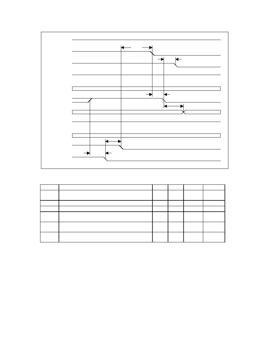
SMSC DS SLC90E66
Page 230
Rev. 07/10/2002
11.3.3.7 On State to Power on Suspend State Timing
FIGURE 19 shows the signal transitions from On state to Power On Suspend state.
FIGURE 19 - ON TO POS
SYM
PARAMETER
MIN
MAX
UNIT
NOTES
t34
nCPU_STP and nPCI_STP Inactive to nSTPCLK
Active
1
RTC
1,2
t35
nSTPCLK Active to nSLP Active
1
RTC
1, 3
t36
nSLP to nSUS_STAT[1-2] Active
2
RTC
1
t37
nSUS_STAT[1-2] Active to nCPU_STP and
nPCI_STP Active
1
RTC
1
t38
nCPU_STP and nPCI_STP Active to nSUS[A]
Active
1
RTC
1
t39
nCPU_STP and nPCI_STP Active to Clocks
Stopped (if applicable)
2
PCICLK
4,5
Note 1: These signals are controlled off an internal RTC clock. 1RTC unit is approximately 32
µ
s.
Note 2: nCPU_STP and nPCI_STP will only be active if system is under clock control.
Note 3: This transition will also wait for the Stop Grant cycle to execute.
Note 4: It is up to the system vendor to determine if nCPU_STP and nPCI_STP signals are used to
control system clocks.
Note 5: See PCICLK requirements for use with PC/PCI DMA and serial IRQs.
Running
Clock Running
Stopped
Inactive
T36
T38
T37
T39
T34
T35
PWROK
nSUS_STAT[1:2]
nSUS[A]
nSUS[B:C]
SUSCLK
nCPU_STP/
nPCI_STP
PCICLK/
CPUCLK
nPCI_RST
CPURST
nSLP
nSTPCLK

SMSC DS SLC90E66
Page 231
Rev. 07/10/2002
11.3.3.8 POS to On Signal Timing (with Processor and PCI Reset)
FIGURE 20 shows the signal transitions from Power On Suspend to On with a full system reset.
FIGURE 20 - POS TO ON (W/ PROCESSOR & PCI RESET)
SYM
PARAMETER
MIN
MAX
UNIT
NOTES
t40
Resume Event to nSUS[A] Inactive
1
RTC
1
t41
Resume Event to nPCI_RST Active
1
RTC
1
t42
Resume Event to CPURST Active
1
RTC
1
t43
Resume Event to nSLP Inactive
1
RTC
1
t44
Resume Event to nSTPCLK Inactive
1
RTC
1
t45
nSUS[A] Inactive to nPCI_STP and nCPU_STP
Inactive
16
ms
2
t46
nPCI_STP and nCPU_STP Inactive to Clocks
Running
2
PCICLK
3
t47
nPCI_STP and nCPU_STP Inactive to
nSUS_STAT[1-2] Inactive
1
ms
t48
nSUS_STAT[1-2] Inactive to nPCI_RST
Inactive
1
RTC
1
t49
nPCI_RST Inactive to nPCI_STP and
nCPU_STP allowed to change
1
RTC
1
t50
nPCI_RST Inactive to CPURST Inactive
1
RTC
1
Note 1:
These signals are controlled off an internal RTC clock. 1RTC unit is approximately 32
µ
s.
Note 2:
This transition requires both a minimum of 16 ms wait for clock synthesizer PLL lock and
PWROK to be active. If PWROK goes Active after 16 ms from nSUS[A-C] inactive, the
transition will occur a minimum of 1 RTC period from PWROK active. PWROK remains
active throughout standard POS system usage.
Note 3:
See PCICLK requirements for use with PC/PCI DMA and serial IRQs.
Running
Clock Stopped
Active
Inactive
T47
T40
T45
T49
T46
T48
T41
T42
T43
T44
T50
Inactive
Clocks Running
Resume Event
PWROK
nSUS_STAT[1:2]
nSUS[A]
nSUS[B:C]
SUSCLK
nCPU_STP/
nPCI_STP
PCICLK/
CPUCLK
nPCI_RST
nSLP
CPURST
nSTPCLK

SMSC DS SLC90E66
Page 232
Rev. 07/10/2002
11.3.3.9 POS to On Signal Timing (with Processor Reset)
FIGURE 21shows the signal transitions from Power On Suspend to On with only a processor reset.
FIGURE 21 - POS TO ON (W/ PROCESSOR RESET)
SYM
PARAMETER
MIN
MAX
UNIT
NOTES
t51
Resume Event to nSUS[A] Inactive
1
RTC
1
t52
Resume Event to CPURST Active
1
RTC
1
t53
Resume Event to nSLP Inactive
1
RTC
1
t54
Resume Event to nSTPCLK Inactive
1
RTC
1
t55
nSUS[A] Inactive to nPCI_STP and nCPU_STP
Inactive
16
ms
2
t56
nPCI_STP and nCPU_STP Inactive to Clocks
Running
2
PCICLK
3
t57
nPCI_STP and nCPU_STP Inactive to
nSUS_STAT[1-2] Inactive
1
ms
t58
nSUS_STAT[1-2] Inactive to nPCI_STP and
nCPU_STP allowed to change
2
RTC
1
t59
nSUS_STAT[1-2] Inactive to CPURST Inactive
2
RTC
1
Note 1: These signals are controlled off an internal RTC clock. 1RTC unit is approximately 32
µ
s.
Note 2: This transition requires both a minimum of 16 ms wait for clock synthesizer PLL lock and
PWROK to be Active. If PWROK goes active after 16 ms from nSUS[A-C] inActive, the transition
will occur a minimum of 1 RTC period from PWROK Active. PWROK remains active throughout
standard POS system usage.
Note 3: See PCICLK requirements for use with PC/PCI DMA and serial IRQs.
Running
Clock Stopped
Active
Inactive
T57
T51
T55
T58
T56
T52
T53
T54
T59
Inactive
Clocks Running
Resume Event
PWROK
nSUS_STAT[1:2]
nSUS[A]
nSUS[B:C]
SUSCLK
nCPU_STP/
nPCI_STP
PCICLK/
CPUCLK
nPCI_RST
nSLP
CPURST
nSTPCLK
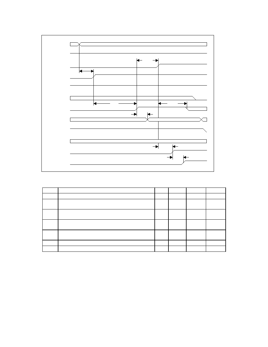
SMSC DS SLC90E66
Page 233
Rev. 07/10/2002
11.3.3.10 POS to On Signal Timing (No Reset)
FIGURE 22 shows the signal transitions from Power On Suspend to On with no reset performed.
FIGURE 22 - POS TO ON (NO RESET)
SYM
PARAMETER
MIN
MAX
UNIT
NOTE
t60
Resume Event to nSUS[A] Inactive
1
RTC
1
t61
nSUS[A] Inactive to nPCI_STP and nCPU_STP
Inactive
16
ms
2
t62
nPCI_STP and nCPU_STP Inactive to Clocks
Running
2
PCICLK
3
t63
nPCI_STP and nCPU_STP Inactive to
nSUS_STAT[1-2] Inactive
1
ms
t64
nSUS_STAT[1-2] Inactive to nPCI_STP and
nCPU_STP allowed to change
2
RTC
1
t65
nSUS_STAT[1:2] Inactive to nSLP Inactive
1
RTC
1
t66
nSUS_STAT[1-2] Inactive to nSTPCLK Inactive
2
RTC
1
Note 1: These signals are controlled off an internal RTC clock. 1RTC unit is approximately 32
µ
s.
Note 2: This transition requires both a minimum of 16 ms wait for clock synthesizer PLL lock and
PWROK to be Active. If PWROK goes active after 16 ms from nSUS[A-C] inActive, the
transition will occur a minimum of 1 RTC period from PWROK Active. PWROK remains
active throughout standard POS system usage.
Note 3: See PCICLK requirements for use with PC/PCI DMA and serial IRQs.
Running
Clock Stopped
T63
T60
T61
T64
T62
Inactive
Clocks Running
Resume Event
PWROK
nSUS_STAT[1:2]
nSUS[A]
nSUS[B:C]
SUSCLK
nCPU_STP/
nPCI_STP
PCICLK/
CPUCLK
nPCI_RST
nSLP
CPURST
nSTPCLK
T65
T66

SMSC DS SLC90E66
Page 234
Rev. 07/10/2002
11.3.3.11 On to STR Signal Timing
FIGURE 23 shows the signal transitions from On state to Suspend to RAM state.
FIGURE 23 - ON TO STR
SYM
PARAMETER
MIN
MAX
UNIT
NOTES
t67
nCPU_STP and nPCI_STP Inactive to
nSTPCLK Active
1
RTC
1,2
t68
nSTPCLK Active to nSLP Active
1
RTC
1,3
t69
nSLP Active to nSUS_STAT[1,2] Active
1
RTC
1
t70
nSUS_STAT[1-2] Active to nCPU_STP and
nPCI_STP Active
1
RTC
1
t71
nCPU_STP and nPCI_STP Active to Clocks
Stopped
2
PCICLK
4,5
t72
nCPU_STP and nPCI_STP Active to
nSUS[A-B] Active
1
RTC
1
t73
nSUS[A-B] Active to PWROK Inactive
0
ns
6
t74
PWROK Inactive to nCPU_STP and
nPCI_STP Float
1
RTC
1
t75
PWROK Inactive to nPCI_RST Active
1
RTC
1
t76
PWROK Inactive to CPURST Active
1
RTC
1
t77
PWROK Inactive to nSLP Inactive
1
RTC
1
t78
PWROK Inactive to nSTPCLK Inactive
1
RTC
1
t79
nCPU_STP and nPCI_STP Float to Clocks
Inavalid
0
ns
7
t80
PWROK Inactive to Core Well Power
Removed
0
ns
Running
Float
Invalid
Inactive
Invalid
Invalid
Invalid
Invalid
T73
T80
T69
T72
T70
T71
T79
T74
T81
T75
T76
T77
T78
T82
T83
T84
T85
T68
T67
Clock Running
Stopped
Active
nSUS_STAT[1:2]
nSUS[A:B]
nSUS[C]
SUSCLK
nCPU_STP/
nPCI_STP
PCICLK/
CPUCLK
nPCI_RST
nSLP
CPURST
nSTPCLK
Core Well Power
PWROK

SMSC DS SLC90E66
Page 235
Rev. 07/10/2002
SYM
PARAMETER
MIN
MAX
UNIT
NOTES
t81
Core Well Power Removed to nPCI_STP
and nCPU_STP Invalid
0
ns
t82
Core Well Power Removed to nPCIRST
Invalid
0
ns
t83
Core Well Power Removed to CPURST
Invalid
0
ns
t84
Core Well Power Removed to nSLP Invalid
0
ns
t85
Core Well Power Removed to nSTPCLK
Invalid
0
ns
Note 1: These signals are controlled off an internal RTC clock. 1RTC unit is approximately 32
µ
s.
Note 2: nCPU_STP and nPCI_STP will only be active if system is under clock control.
Note 3: This transition will also wait for the Stop Grant cycle to execute.
Note 4: It is up to the system vendor to determine if nCPU_STP and nPCI_STP signals are used to
control system clocks.
Note 5: See PCICLK requirements for use with PC/PCI DMA and serial IRQs.
Note 6: It is up to the system vendor to determine if nSUS[A-B] signals are used to control system
power planes. If power remains applied to system board and PWROK stays alive during
STR, the SLC90E66 signals will remain in the states shown after t73.
Note 7: Clocks may or may not be running depending on condition of Power Supply Voltages.

SMSC DS SLC90E66
Page 236
Rev. 07/10/2002
11.3.3.12 STR to On Signal Timing
FIGURE 24 shows the system transition from Suspend To RAM to On with a full system reset.
FIGURE 24 - STR TO ON
SYM
PARAMETER
MIN
MAX
UNIT
NOTES
t86
Resume Event to nSUS[A-B] Inactive
1
RTC
1
t87
nSUS[A-B] Inactive to Core Well Power Applied
0
ns
t88
Core Well Power Applied to nPCI_STP and
nCPU_STP Float
0
ns
t89
Core Well Power Applied to nPCI_RST Active
0
ns
t90
Core Well Power Applied to CPURST Active
0
ns
t91
Core Well Power Applied to nSLP Inactive
0
ns
t92
Core Well Power Applied to nSTPCLK Inactive
0
ns
t93
nPCI_STP and nCPU_STP Float to Clocks
Running
2
t94
Core Well Power Applied to PWROK Active
1
ms
t95
PWROK Active to nCPU_STP and nPCI_STP
Active
0
ns
t96
nPCI_STP and nCPU_STP Active to Clocks
Stopped
2
PCICLK
3
t97
PWROK Active to nCPU_STP and nPCI_STP
Inactive
1
RTC
1
Running
Invalid
Float
Invalid
Running
Stopped
Running
Invalid
Invalid
Active
Inactive
Invalid
Invalid
T86
T87
T94
T100
T98
T88
T95
T97
T93
T96
T101
T99
T101a
T102
T89
T90
T91
T92
nSUS_STAT[1:2]
nSUS[A:B]
nSUS[C]
SUSCLK
nCPU_STP/
nPCI_STP
PCICLK/
CPUCLK
nPCI_RST
nSLP
CPURST
nSTPCLK
Core Well Power
PWROK
Resume Event
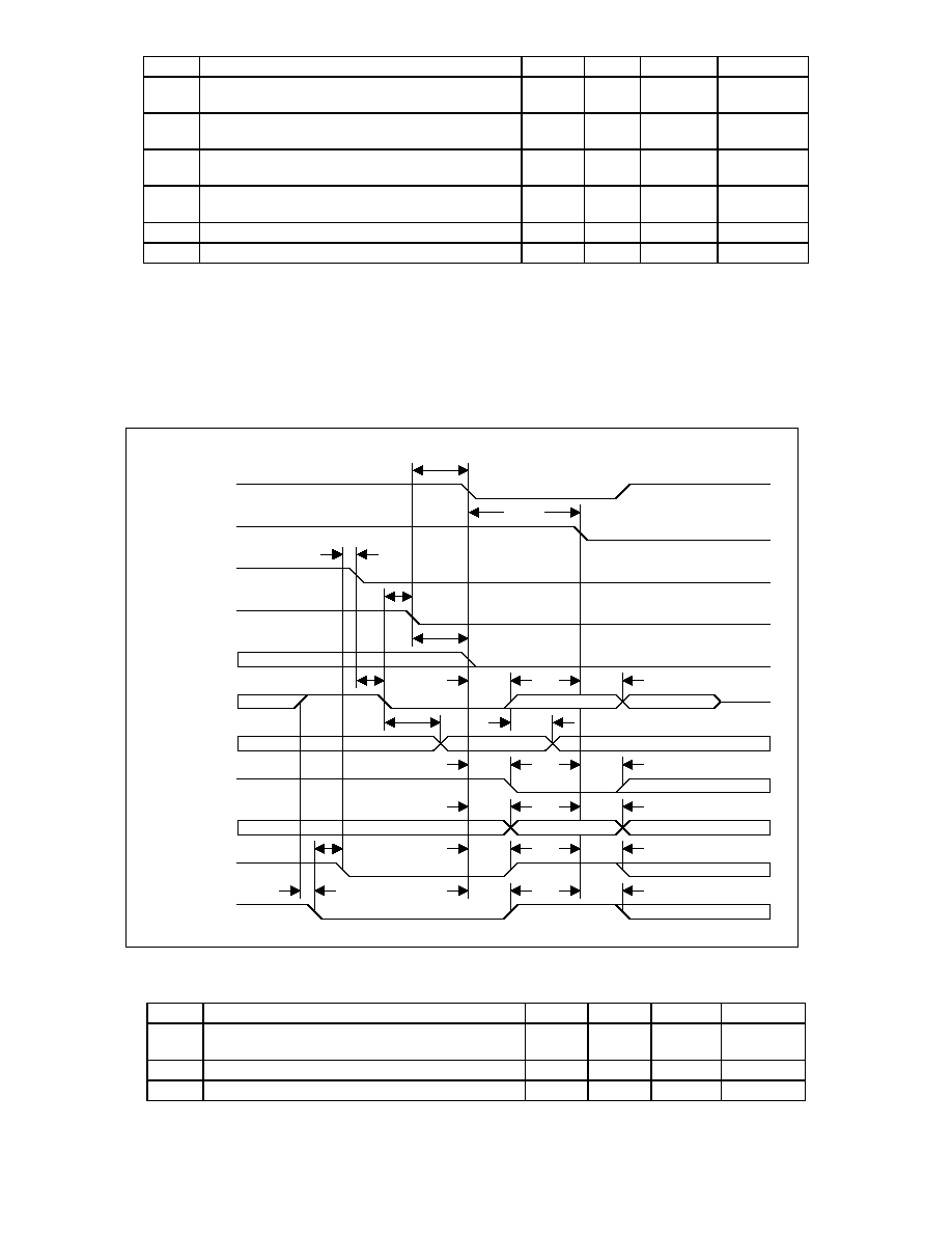
SMSC DS SLC90E66
Page 237
Rev. 07/10/2002
SYM
PARAMETER
MIN
MAX
UNIT
NOTES
t98
nSUS[A-B] Inactive to nCPU_STP and
nPCI_STP Inactive
16
ms
t99
nCPU_STP and nPCI_STP Inactive to Clocks
Running
2
PCICLK
3
t100
nCPU_STP and nPCI_STP Inactive to
nSUS_STAT[1-2] Inactive
1
ms
t101
nSUS_STAT[1-2] Inactive to nCPU_STP and
nPCI_STP allowed to change
2
RTC
1
t101a
nSUS_STAT[1-2] Inactive to nPCI_RST Inactive
1
RTC
1
t102
nPCI_RST Inactive to CPURST Inactive
1
RTC
1
Note 1: These signals are controlled off an internal RTC clock. 1RTC unit is approximately 32
µ
s.
Note 2: There are no specific requirements for these timings related to the SLC90E66. The system
manufacturer should make sure that the clocks on power up meet any other system
specification. As a minimum, the clocks must be available and stable after time t99.
Note 3: See PCICLK requirements for use with PC/PCI DMA and serial IRQs.
11.3.3.13 On to STD / SOFF Signal Timing
FIGURE 25shows the signal transitions from On state to Suspend to Disk or Soft Off state.
FIGURE 25 - ON TO STD / SOFF
SYM
PARAMETER
MIN
MAX
UNIT
NOTES
t103
nCPU_STP and nPCI_STP Inactive to nSTPCLK
Active
1
RTC
1, 2
t104
nSTPCLK Active to nSLP Active
1
RTC
1, 3
t105
nSLP Active to nSUS_STAT[1,2] Active
2
RTC
1
Running
Invalid
Running
Stopped
Invalid
Inactive
Invalid
Invalid
Invalid
Invalid
T110
T117
T103
T108
T106
T107
T111
T118
T116
T119
T112
T113
T114
T115
T120
T121
T122
T104
T105
Active
Float
nSUS_STAT[1:2]
nSUS[A:C]
SUSCLK
nCPU_STP/
nPCI_STP
PCICLK/
CPUCLK
nPCI_RST
nSLP
CPURST
nSTPCLK
Core Well Power
PWROK
T109

SMSC DS SLC90E66
Page 238
Rev. 07/10/2002
SYM
PARAMETER
MIN
MAX
UNIT
NOTES
t106
nSUS_STAT[1-2] Active to nCPU_STP and
nPCI_STP Active
1
RTC
1
t107
nCPU_STP and nPCI_STP Active to Clocks
Stopped
2
PCICLK
1,4,5
t108
nCPU_STP and nPCI_STP Active to nSUS[A-C]
Active
1
RTC
1
t109
nSUS[A-C] Active to SUSCLK Low
1
RTC
1
t110
nSUS[A-C] Active to PWROK Inactive
0
ns
6
t111
PWROK Inactive to nCPU_STP and nPCI_STP
Float
1
RTC
1
t112
PWROK Inactive to nPCI_RST Active
1
RTC
1
t113
PWROK Inactive to CPURST Active
1
RTC
1
t114
PWROK Inactive to nSLP Inactive
1
RTC
1
t115
PWROK Inactive to nSTPCLK Inactive
1
RTC
1
t116
nCPU_STP and nPCI_STP Float to Clocks
Inavalid
0
ns
t117
PWROK Inactive to Core Well Power Removed
0
ns
t118
Core Well Power Removed to nPCI_STP and
nCPU_STP Invalid
0
ns
t119
Core Well Power Removed to nPCIRST Invalid
0
ns
t120
Core Well Power Removed to CPURST Invalid
0
ns
t121
Core Well Power Removed to nSLP Invalid
0
ns
t122
Core Well Power Removed to nSTPCLK Invalid
0
ns
Note 1: These signals are controlled off an internal RTC clock. 1RTC unit is approximately 32
µ
s.
Note 2: nCPU_STP and nPCI_STP will only be Active if system is under clock control.
Note 3: This transition will also wait for the Stop Grant cycle to execute.
Note 4: It is up to the system vendor to determine if nCPU_STP and nPCI_STP signals are used to
control system clocks.
Note 5: See PCICLK requirements for use with PC/PCI DMA and serial IRQs.
Note 6: It is up to the system vendor to determine if nSUS[A-C] signals are used to control system
power planes. If power remains applied to system board and PWROK stays alive during
STR, the SLC90E66 signals will remain in the states shown after t110.
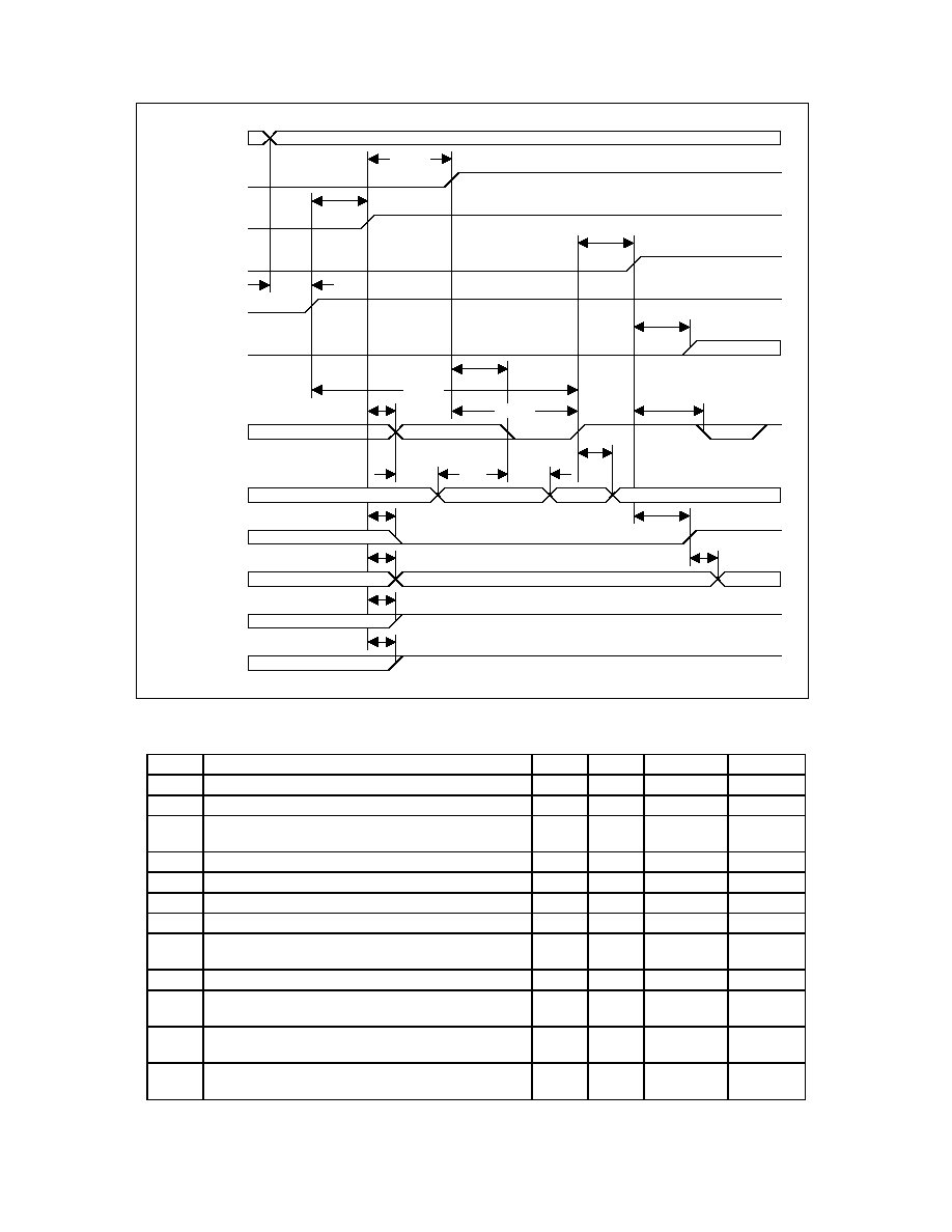
SMSC DS SLC90E66
Page 239
Rev. 07/10/2002
11.3.3.14 STD / SOFF to On Signal Timing
FIGURE 26 shows the system transition from Suspend To Disk to On with a full system reset.
FIGURE 26 - STD/ SOFF TO ON
SYM
PARAMETER
MIN
MAX
UNIT
NOTES
t123
Resume Event to nSUS[A-C] Inactive
1
RTC
1
t124
nSUS[A-C] Inactive to Core Well Power Applied
0
ns
t125
Core Well Power Applied to nPCI_STP and
nCPU_STP Float
0
ns
t126
Core Well Power Applied to nPCI_RST Active
0
ns
t127
Core Well Power Applied to CPURST Active
0
ns
t128
Core Well Power Applied to nSLP Inactive
0
ns
t129
Core Well Power Applied to nSTPCLK Inactive
0
ns
t130
nPCI_STP and nCPU_STP Float to Clocks
Running
2
t131
Core Well Power Applied to PWROK Active
1
ms
t132
PWROK Active to nCPU_STP and nPCI_STP
Active
0
ns
t133
nPCI_STP and nCPU_STP Active to Clocks
Stopped
2
PCICLK
3
t134
nSUS[A-C] Inactive to nCPU_STP and nPCI_STP
Inactive
16
ms
Running
Invalid
Float
T131
T124
T125
T137
T138
T123
T135
T134
T132
Invalid
Running
Stopped
Running
Invalid
Invalid
Invalid
Invalid
Active
Inactive
T130
T133
T136
T140
T126
T127
T128
T129
T139
T141
nSUS_STAT[1:2]
nSUS[A:C]
SUSCLK
nCPU_STP/
nPCI_STP
PCICLK/
CPUCLK
nPCI_RST
nSLP
CPURST
nSTPCLK
Core Well Power
PWROK
Resume Event

SMSC DS SLC90E66
Page 240
Rev. 07/10/2002
SYM
PARAMETER
MIN
MAX
UNIT
NOTES
t135
PWROK Active to nCPU_STP and nPCI_STP
Inactive
1
RTC
1
t136
nCPU_STP and nPCI_STP Inactive to Clocks
Running
1
2
PCICLK
3
t137
nCPU_STP and nPCI_STP Inactive to
nSUS_STAT[1-2] Inactive
1
ms
t138
nSUS_STAT[1-2] Inactive to SUSCLK Running
1
RTC
1
t139
nSUS_STAT[1-2] Inactive to nPCI_RST Inactive
1
RTC
1
t140
nSUS_STAT[1-2] Inactive to nCPU_STP and
nPCI_STP allowed to change
2
RTC
1
t141
nPCI_RST Inactive to CPURST Inactive
1
RTC
1
Note 1: These signals are controlled off an internal RTC clock. 1RTC unit is approximately 32
µ
s.
Note 2: There are no specific requirements for these timings related to the SLC90E66. The system
manufacturer should make sure that the clocks on power up meet any other system
specification. As a minimum, the clocks must be available and stable after time t136.
Note 3: See PCICLK requirements for use with PC/PCI DMA and serial IRQs.
11.3.4 ALTERNATE AT REGISTER ACCESS MODE (SHADOW REGISTERS)
The SLC90E66 implements a shadow mechanism for storing the data written to the AT write-only registers. An
"Alternate AT Register Access Mode" is also implemented so that, in the transition to Suspend mode, the contents of
these registers can be read and saved to non-volatile memory so the system state can be restored when resumed.
Once placed in the "Alternate Access" mode, the SLC90E66 allows various registers that would otherwise be
inaccessible be read and written. To enable the Alternate Access mode, set Bit 5, Register 0B0h of the SLC90E66
PCI Function 0 to a 1. Table 38 through Table 41 show the changes to read and write accesses to the various
functions.
Since there are no provisions are made for stopping events from occurring while the BIOS is reading or restoring
register values, the BIOS should exercise with great care while using this feature. For example, when reading the
status of the DMA controller, all DMA channels should be temporarily masked.
It is assumed that no other accesses to the module will be permitted once in ALT Access mode.
Table 38 - DMA Controller Registers In Alternate Access Mode
I/O ADDRESS
R/W
MODE
STANDARD MODE USAGE
ALT ACCESS MODE
0000h
W
Base Address for Channel 0
Current Address for Channel 0
0000h
R
Current Address for Channel 0
Base Address for Channel 0
0001h
W
Base Byte Count for Channel 0
Current Byte Count for Channel 0
0001h
R
Current Byte Count for Channel
0
Base Byte Count for Channel 0
0002h
W
Base Address for Channel 1
Current Address for Channel 1
0002h
R
Current Address for Channel 1
Base Address for Channel 1
0003h
W
Base Byte Count for Channel 1
Current Byte Count for Channel 1
0003h
R
Current Byte Count for Channel
1
Base Byte Count for Channel 1
0004h
W
Base Address for Channel 2
Current Address for Channel 2
0004h
R
Current Address for Channel 2
Base Address for Channel 2
0005h
W
Base Byte Count for Channel 2
Current Byte Count for Channel 2
0005h
R
Current Byte Count for Channel
2
Base Byte Count for Channel 2
0006h
W
Base Address for Channel 3
Current Address for Channel 3
0006h
R
Current Address for Channel 3
Base Address for Channel 3
0007h
W
Base Byte Count for Channel 3
Current Byte Count for Channel 3

SMSC DS SLC90E66
Page 241
Rev. 07/10/2002
I/O ADDRESS
R/W
MODE
STANDARD MODE USAGE
ALT ACCESS MODE
0007h
R
Current Byte Count for Channel
3
Base Byte Count for Channel 3
0008h
W
Command Register (Ch. 0-3)
Status Register (Ch. 0-3)
0008h
R
Status Register (Ch. 0-3)
1
st
Read: Command Register (Ch.
0-3)
2
nd
Read: Request Register (Ch. 0-
3)
3
rd
Read: Mode Register (Ch 0)
4
th
Read: Mode Register (Ch 1)
5
th
Read: Mode Register (Ch 2)
6
th
Read: Mode Register (Ch 3)
0009h
W
Request Register (Ch 0-3)
Reserved
0009h
R
Reserved
Reserved
000Ah
W
Write Single Mask (Ch 0-3)
Reserved
000Ah
R
Reserved
Reserved
000Bh
W
Mode Register (Ch 0-3)
Reserved
000Bh
R
Reserved
Reserved
000Ch
W
Clear Byte Pointer
Clear Byte Pointer
000Ch
R
Reserved
Reserved
000Dh
W
Master Clear
Master Clear
000Dh
R
Reserved
Reserved
000Eh
W
Clear Masks
Clear Masks
000Eh
R
Reserved
Reserved
000Fh
W
Write All Masks (0-3)
Write All Masks (0-3)
000Fh
R
Reserved
Read All Masks (0-3)
DMA CONTROLLER 2 (16 BIT)
00C0h
W
Base Address for Channel 4
Current Address for Channel 4
00C0h
R
Current Address for Channel 4
Base Address for Channel 4
00C2h
W
Base Word Count for Channel
4
Current Word Count for Channel 4
00C2h
R
Current Word Count for
Channel 4
Base Word Count for Channel 4
00C4h
W
Base Address for Channel 5
Current Address for Channel 5
00C4h
R
Current Address for Channel 5
Base Address for Channel 5
00C6h
W
Base Word Count for Channel
5
Current Word Count for Channel 5
00C6h
R
Current Word Count for
Channel 5
Base Word Count for Channel 5
00C8h
W
Base Address for Channel 6
Current Address for Channel 6
00C8h
R
Current Address for Channel 6
Base Address for Channel 6
00CAh
W
Base Word Count for Channel
6
Current Word Count for Channel 6
00CAh
R
Current Word Count for
Channel 6
Base Word Count for Channel 6
00CCh
W
Base Address for Channel 7
Current Address for Channel 7
00CCh
R
Current Address for Channel 7
Base Address for Channel 7
00CEh
W
Base Word Count for Channel
7
Current Word Count for Channel 7
00CEh
R
Current Word Count for
Channel 7
Base Word Count for Channel 7
00D0h
W
Command Register (Ch. 4-7)
Status Register (Ch. 4-7)

SMSC DS SLC90E66
Page 242
Rev. 07/10/2002
I/O ADDRESS
R/W
MODE
STANDARD MODE USAGE
ALT ACCESS MODE
00D0h
R
Status Register (Ch. 4-7)
1
st
Read: Command Register (Ch.
4-7)
2
nd
Read: Request Register (Ch. 4-
7)
3
rd
Read: Mode Register (Ch 4)
4
th
Read: Mode Register (Ch 5)
5
th
Read: Mode Register (Ch 6)
6
th
Read: Mode Register (Ch 7)
00D2h
W
Request Register (Ch 4-7)
Reserved
00D2h
R
Reserved
Reserved
00D4h
W
Write Single Mask (Ch 4-7)
Reserved
00D4h
R
Reserved
Reserved
00D6h
W
Mode Register (Ch 4-7)
Reserved
00D6h
R
Reserved
Reserved
00D8h
W
Clear Byte Pointer
Clear Byte Pointer
00D8h
R
Reserved
Reserved
00DAh
W
Master Clear
Master Clear
00DAh
R
Reserved
Reserved
00DCh
W
Clear Masks
Clear Masks
00DCh
R
Reserved
Reserved
00DEh
W
Write All Masks (4-7)
Write All Masks (4-7)
00DEh
R
Reserved
Read All Masks (4-7)
Note: The Alternate Access Mode allows reading and restoring all of the initial base address and byte/word
counts. Also makes it possible to read command, mode, and mask registers, as well as restore status, mode and
mask registers.
Table 39 - NMI Enable Bit Changes in Alternate Access Mode
I/O ADDRESS
R/W
MODE
STANDARD MODE USAGE
ALT ACCESS MODE
0070h
(bit7 only)
R
Invalid
Bit 7 (NMI Enable Bit) value is
returned.

SMSC DS SLC90E66
Page 243
Rev. 07/10/2002
Table 40 - Programmable Interval Timer Changes In Alternate Access Mode
I/O ADDRESS
R/W
MODE
STANDARD MODE USAGE
ALT ACCESS MODE
0040h
R
Status Byte Counter 0.
1
st
Read: Status Byte Counter 0.
2
nd
Read: CR
L
for Counter 0.
3
rd
Read: CR
M
for Counter 0.
4
th
Read: CR
L
for Counter 1.
5
th
Read: CR
M
for Counter 1.
6
th
Read: CR
L
for Counter 2.
7
th
Read: CR
M
for Counter 2.
0041h
R
Status Byte Counter 1.
Status Byte Counter 1.
0042h
R
Status Byte Counter 2.
Status Byte Counter 2.
The BIOS must perform seven consecutive reads from port 40h in alternate access mode. If BIOS deviates from this,
it may get inaccurate data. It also allows BIOS to configure the Alternate Access Mode and still read the status of all
the counters. Setting the Alternate Access Mode automatically clears the high/low flip flop. When the Alternate
Access mode is entered the timers do not stop counting, hence the current values will change from the time the initial
value is read.
Table 41 - Programmable Interrupt Controller
I/O ADDRESS
R/W
MODE
STANDARD MODE USAGE
ALT ACCESS MODE
0020h
R
Interrupt Request Register for
Controller 1.
1
st
Read: ICW1 for Controller 1
2
nd
Read: ICW2 for Controller 1
3
rd
Read: ICW3 for Controller 1
4
th
Read: ICW4 for Controller 1
5
th
Read: OCW1 for Controller 1
6
th
Read: OCW2 for Controller 1
7
th
Read: OCW3 for Controller 1
8
th
Read: ICW1 for Controller 2
9
th
Read: ICW2 for Controller 2
10
th
Read: ICW3 for Controller 2
11
th
Read: ICW4 for Controller 2
12
th
Read: OCW1 for Controller 2
13
th
Read: OCW2 for Controller 2
14
th
Read: OCW3 for Controller 2
0021h
R
In-Service Register for Controller 1.
In-Service Register for Controller 1.
00A0h
R
Interrupt Request Register for
Controller 2.
Interrupt Request Register for Controller
2.
00A1h
R
In-Service Register for Controller 2.
In-Service Register for Controller 2.
11.4 System Management
The SLC90E66 system management function provides mechanisms to communicate detected system activities to
system management software and to communicate with other devices on the system board. Communication with
system software is through the System Management Interrupt (SMI) mechanism, and an integrated System
Management Bus host and slave controller can be used to communicate with on-board devices.
11.4.1 SMI ASSERTION
MECHANISM
System Management Interrupts are generated to the processor through the assertion of the nSMI signal. Various
system events, described below, will cause nSMI to be asserted if enabled.
SMI generation is enabled by setting the [SMI_EN] bit, bit 0 of GLBCTL IO Register, and controlled by the End of SMI
[EOS] bit, bit 16 of GLBCTL IO Register. The EOS bit is first set to enable the generation of the first SMI. When an
enabled nSMI generation event occurs, the EOS bit is reset to 0. When this bit is cleared the nSMI signal is asserted.
The processor will then enter System Management Mode and the SMI handler will service all requesting SMIs. If an

SMSC DS SLC90E66
Page 244
Rev. 07/10/2002
SMI event occurs while the SLC90E66 has this bit (EOS) cleared, then no additional SMIs to the processor are
generated, however the appropriate status bits will be set. At the end of the SMI handler, the software will set this bit.
When the bit is set, the SLC90E66 will drive the nSMI signal inactive for a minimum of one PCI clock. The
combination of this bit being set, and another SMI request being active (one of the SMI status bits is set) will cause
the SLC90E66 to reset [EOS] bit again and re-assert the SMI signal to the processor.
It is important to know that EOS bit will not get set until all SMI status bits are cleared. Therefore, before exiting, the
SMI handler must verify that the bit is successfully set. Otherwise, there could be another pending SMI that will
prevent the EOS bit from being set. In this case, the SMI handler should clear that SMI status bit and set the EOS bit
again.
11.4.2 NSMI
GENERATION EVENTS
Some of the nSMI generation events may also generate the ACPI compatible System Control Interrupt (SCI) or
suspend state resume events. The nSMI or SCI is selectable through the [SCI_EN] bit, which is bit 0 of the
PMCNTRL IO Register. When the bit is set to 1, these events will generate an SCI if enabled. When the bit is reset,
these events will generate an nSMI if enabled.
When an nSMI event occurs, a status bit is set. The status bits from various sources are combined together to create
hierarchical status bits. The hierarchical status bits cannot be reset through software. Their respective "children"
status bits must all be cleared in order for them to clear.
The nSMI generation events include:
§
nPWRBTN
Assertion
§
LID
Assertion
§
nGPI1
Assertion
§
EXTnSMI
Asssertion.
§
SMBus
Events
§
Global Standby Timer Expiration.
§
PCI Bus Master Requests.
§
APMC Control Register Writes
§
USB Legacy Keyboard/Mouse Event.
§
Software Timer SMI.
§
Device Monitor Trap.
§
Device Monitor Idle Timer Expiration.
§
SLC90E66 Master Abort on PCI
§
Global
Release.
§
Thermal Alarm (nTHRM Assertion).
11.4.2.1 nPWRBTN Assertion Event
The nPWRBTN input signal can be used to generate an nSMI upon its assertion. It contains a 170ms debounce
circuit to filter out mechanical switch bounce. When asserted, it will set the [PWRBTN_STS] bit after the 170ms
debounce. This will cause generation of an nSMI if enabled. If the nPWRBTN signal is held active for greater than 4
seconds and Power Button Override feature is enabled, the [PWRBTN_STS] bit is cleared, the [PWRBTNOR_STS]
bit is set, and the SLC90E66 will automatically transition the system into the Soft Off Suspend state. This signal can
also be used to generate an SCI or a suspend state resume event.
In a suspend state, the assertion of nPWRBTN signal will always set the PWRBTN_STS bit and generate a resume
event causing the SLC90E66 to initiate a resume sequence.
Enable Bits:
[PWRBTN_EN]
Bit 8 of PMEN IO Register (Base + 02h)
[PWRBTNOR_EN]
Bit 9 of PMCNTRL IO Register ( Base + 04h)
Status Bits:
[PWRBTN_STS]
Bit 8 of PMSTS IO Register (Base + 00h)
[PWRBTNOR_STS]
Bit 11 of PMSTS IO Register (Base + 00h)

SMSC DS SLC90E66
Page 245
Rev. 07/10/2002
11.4.2.2 LID Assertion Event
The LID signal, when asserted, will set the [LID_STS] bit after a 170ms debounce, and when enabled will generate
an nSMI. The assertion polarity can be controlled to allow system code to detect when LID signal transistions from
low to high or high to low. This signal can also be used to generate an SCI or a suspend state resume event.
Enable Bit:
[LID_EN]
Bit 11 of GPEN IO Register (Base + 0Eh)
Polarity Select:
[LID_POL]
Bit 25 of GLBCTL IO Register (Base + 28h)
Status Bits:
[LID_STS]
Bit 11 of GPSTS IO Register (Base + 0Ch)
11.4.2.3 nGPI1 Assertion Event
The nGPI1 signal, when asserted LOW, will set the [GPI_STS] bit, and when enabled will generate an nSMI. This
signal can also be used to generate an SCI or a suspend state resume event.
Enable Bit:
[GPI_EN]
Bit 9 of GPEN IO Register (Base + 0Eh)
Status Bit:
[GPI_STS]
Bit 9 of GPSTS IO Register (Base + 0Ch)
11.4.2.4 nEXTSMI Assertion Event
The nEXTSMI signal, when asserted LOW, will set the [EXTSMI_STS] bit, and when enabled will generate an nSMI.
This signal can also be used to generate an SCI or a suspend state resume event.
Enable Bit:
[EXTSMI_EN]
Bit 10 of GLBEN IO Register (Base + 20h)
Status Bit:
[EXTSMI_STS]
Bit 10 of GLBSTS IO Register (Base + 18h)
11.4.2.5 SMBus
Events
The SMBus Controller has several ways to generate an nSMI. They can also be used to generate a suspend state
resume event. See SMBus Functional Description for additional information.
Enable Bits: [ALERT_EN]
Bit 3 of SMBSLVCNT SMBus IO Register (Base + 08h)
[SLV_EN]
Bit 0 of SMBSLVCNT SMBus IO Register (Base + 08h)
[SHDW1_EN]
Bit 1 of SMBSLVCNT SMBus IO Register (Base + 08h)
[SHDW2_EN]
Bit 2 of SMBSLVCNT SMBus IO Register (Base + 08h)
Status Bits:
[ALERT_STS]
Bit 5 of SMBSLVSTS SMBus IO Register (Base + 01h)
[SLV_STS]
Bit 2 of SMBSLVSTS SMBus IO Register (Base + 01h)
[SHDW1_STS]
Bit 3 of SMBSLVSTS SMBus IO Register (Base + 01h)
[SHDW2_STS]
Bit 4 of SMBSLVSTS SMBus IO Register (Base + 01h)
11.4.2.6 Global Standby Timer Expiration Event
The Global Standby Timer will set the [GSTBY_STS] bit upon expiration, and if enabled will generate an nSMI. It can
also be used to generate a suspend state resume event.
Enable Bits:
[GSTBY_EN]
Bit 8 of GLBEN IO Register (Base + 20h)
Status Bits:
[GSTBY_STS]
Bit 8 of GLBSTS IO Register (Base + 18h)
11.4.2.7 PCI Bus Master Requests Event
Assertion of nPCIREQ[A-D] or nPHOLD will generate an nSMI if enabled. This can also cause idle, burst, or global
standby timer reloads as part of Device 8 Monitor logic.
Enable Bits:
[BM_TRP_EN]
Bit 3 of GLBEN IO Register (Base + 20h)
[BM_RLD_DEV8]
Bit 27 of DEVCTL IO Register (Base + 2Ch)
Status Bit:
[BM_STS]
Bit 4 of PMSTS IO Register (Base + 00h)
11.4.2.8 APMC Control Register Writes
Writes to the APM Control Register (APMC, IO port B2h) will generate an nSMI if enabled.
Enable Bit:
[APMC_EN]
Bit 25 of DEVACTB PCI Configuration Register (58-5Bh)
Status Bit:
[APM_STS]
Bit 5 of GLBSTS IO Register (Base + 18h)
11.4.2.9 USB Legacy Keyboard/Mouse Event (Not Implemented Yet)
The USB Legacy Keyboard logic uses nSMI generation as part of its operation. The [LEGACY_USB_EN] bit must be
set active in order for USB Legacy Keyboard to function.
Enable Bit:
[LEGACY_USB_EN]
Bit 0 of GLBEN IO Register (Base + 20h)
Status Bit:
[LEGACY_USB_STS]
Bit 1 of GLBSTS IO Register (Base + 18h)

SMSC DS SLC90E66
Page 246
Rev. 07/10/2002
.
11.4.2.10 Software Timer SMI Event
The Idle Timer for Device 3 Monitor can be used as a Software SMI Timer. If the Idle Timer reload events are
disabled (via [IDL_RLD_EN_DEV3] bit), the timer will count down without reload and its expiration will generate an
nSMI.
Enable Bit:
[IDL_EN_DEV3]
Bit 6 of DEVCTL IO Register (Base + 2Ch)
[IDL_RLD_EN_DEV3]
Bit 26 of DEVCTL IO Register (Base + 2Ch)
Status Bit:
[IDL_STS_DEV3]
Bit 3 of DEVSTS IO Register (Base + 1Ch)
11.4.2.11 Device Trap Event
The IO Trap for Device Monitoring subsystem will generate an nSMI when the programmed trap event occurs. The
[DEV_STS] bit is a logical OR of [TRAP_STS_DEVx] and [IDL_STS_DEVx] bits.
Enable Bit:
[TRAP_EN_DEVx]
See DEVCTL IO Register (Base + 2Ch)
Status Bits:
[TRAP_STS_DEVx]
See DEVSTS IO Register (Base + 1Ch)
[DEV_STS]
Bit 4 of GLBSTS IO Register (Base + 18h) where x = 0-13
11.4.2.12 Device Idle Timer Expiration Event
The Idle Timers for Device Monitoring subsystem will count down and generate an nSMI upon expiration if enabled.
The [DEV_STS] bit is logical "OR" of [TRP_STS_DEVx] and [IDL_STS_DEVx] bits.
Enable Bits:
[IDL_EN_DEVx]
See DEVCTL IO Register (Base + 2Ch)
Status Bits:
[IDL_STS_DEVx]
Bits[11-0] of DEVSTS IO Register (Base + 1Ch)
[DEV_STS]
Bit 4 of GLBSTS IO Register (Base +18h) where x = 0-11.
11.4.2.13 SLC90E66 Master Abort on PCI
A Master Abort to the SLC90E66 initiated PCI cycle will generate an nSMI if enabled.
Enable Bits:
[SBMA_EN]
Bit 4 of GLBEN IO Register (Base + 20h)
Status Bits:
[SBMA_STS]
Bit 2 of GLBSTS IO Register (Base + 18h)
11.4.2.14 Global Release Event
Writes to the Power Management I Control Register (PM1_CNTRL) with bit 2 set will generate an nSMI if enabled.
See ACPI Support section for more information.
Enable Bits:
[BIOS_EN]
Bit 1 of GLBEN IO Register (Base + 20h)
Status Bits:
[BIOS_STS]
Bit 0 of GLBSTS IO Register (Base + 18h)
11.4.2.15 Thermal Alarm Event (nTHRM Assertion)
The nTHRM signal will set the [THRM_STS] bit when asserted and if enabled will generate an nSMI. The assertion
polarity can be programmed to allow system code to detect when nTHRM signal transitions from low to high or high
to low. This signal can also be used to generate an SCI. When asserted, the nTHRM will also cause automatic clock
throttling, which is independent of the [THEM_EN] control bit.
Enable Bit:
[THEM_EN]
Bit 0 of GPEN IO Register (Base + 0Eh)
Polarity Select:
[THRM_POL]
Bit 2 of GLBCTL IO Register (Base + 28h)
Status Bit:
[THEM_STS]
Bit 0 of GPSTS IO Register (Base + 0Ch)
11.4.3 GLOBAL STANDBY
TIMER
The Global Standby Timer is used to monitor global system activity during normal operation and can be reloaded by
system activity events. When enabled, the timer will load and start counting down. Enabled system events will cause
the timer to reload its initial value and begin counting down again. If no system events reload the timer, it will
eventually count to zero. Upon this expiration, it generates an nSMI. When the system is placed in a Suspend Mode,
the Global Standby Timer can also be used to generate a resume event.

SMSC DS SLC90E66
Page 247
Rev. 07/10/2002
The Global Standby Timer stops counting when the SM_FREEZE bit is set. This can be used to keep it from counting
down when the system is executing an SM routine. The SM_FREEZE bit is disregarded while in a Suspend state, so
that the Global Standby Timer will count down independent of the SM_FREEZE value.
Global Standby Timer Programming Information:
Resolution: 4 milliseconds, 4 seconds, 32 seconds or 4 minutes
[GSTBY_SELA] Bit 8 of GLBCTL IO Register (Base+28h)
[GSTBY_SELB] Bit 26 of GLBCTL IO Register
Count (7-bits):
[GSTBY_CNT]
Bit[15-9] of GLBCTL IO Register
Counter and nSMI Enable:
[GSTBY_EN]
Bit 8 of GLBEN IO Register (Base+20h)
Expiration Status:
[GSTBY_STS]
Bit 8 of GLBSTS IO Register (Base+18h)
Global Standby Timer Reload Events and The Control Register Bits:
IRQ1, IRQ12/M
[GRLD_EN_KBC_MS]
Bit 2 of DEVACTB PCI Register (58h-5Bh)
NMI, INIT, IRQ[1,3-7,9-15]:
[GRLD_EN_IRQ]
Bit 6 of DEVACTB PCI Register (58h-5Bh)
Device 0-13 Monitors:
[GRLD_EN_DEVx]
Bit [13-0] of DEVACTA PCI Reg.(54h-57h)
Video Monitor (PCI Bus Utilization):
[VIDEO_EN]
Bit 24 of DEVACTB PCI Reg. (58h-5Bh)
PCI Bus Master Activity:
[BM_RLD_DEV8]-
Bit 27 of DEVCTL IO Register (Base+2Ch)
[GRLD_EN_DEV8]
Bit 8 of DEVACTA PCI Reg. (54h-57h)
11.5 ACPI Support
The SLC90E66 fully supports the ACPI specification, including the ACPI I/O register mapping, the SCI interrupt and a
Power Management Timer. A semaphore mechanism is also implemented to coordinate access to the power
management resources by either ACPI or the BIOS.
11.5.1 SCI
GENERATION
The nPWRBTN, nGPI1, nTHRM, and LID events can be enabled to generate the ACPI interrupt, SCI (IRQ9) or an
nSMI. The nSMI or SCI is selectable with the [SCI_EN] bit. When set to 1, an enabled event will generate an SCI.
SCI Generation Events Control Bits
nPWRBTN Asserted
[PWRBTN_EN]
GPI1 Asserted
[GPI_EN]
Thermal Alarm (nTHRM Assertion)
[THRM_EN]
-Polarity Select
[THRM_POL]
LID Asserted
[LID_EN]
-Polarity Select
[LID_POL]
Power Management Timer Overflow
[TMROF_EN]
BIOS Release
[GLB_EN]
11.5.2 POWER MANAGEMENT TIMER
The SLC90E66 integrates an ACPI compatible power management timer. The timer consists of a free running
counter (with a 14.31818/4, or 3.579545MHz clock source), a timer register, and a single interrupt source. This circuit
is illustrated in FIGURE 27. The interrupt source is used to indicate that the counter has changed bit 23 high to low or
low to high, this condition generates a System Control Interrupt (SCI). The overflow interrupt is used by ACPI
software to understand when the timer is about to overflow, and allows software to emulate a larger timer.

SMSC DS SLC90E66
Page 248
Rev. 07/10/2002
3.57954 MHz
TMROF_STS
PM1_STS.0
PMTMR_SCI
TMROF_EN
PM1_EN.0
24 Bit
TMR_VAL
PM1_TMR[23-0]
24 Bit
Counter
PM Timer
State Machine
FIGURE 27 - POWER MANAGEMENT TIMER
Power Management Timer Programming:
Clock Frequency:
3.579545 MHz (14.31818/4)
Timer Value:
[TMR_VAL]
Timer Overflow Status:
[TMROF_STS]
SCI Generation Control:
[TMROF_EN]
11.5.3 GLOBAL LOCK MECHANISM
If the BIOS and ACPI software will share resources through a common I/O port, a Global Lock mechanism must be
applied as a semaphore to arbitrate to these shared resources. For example, if both the BIOS and the ACPI driver
share the same system management microcontroller I/O ports to manage the system, the access must be controlled
through the Global Lock mechanism.
If the BIOS attempts to use the shared resources and there is a conflict, the Global Lock logic is used by the ACPI
driver to inform the BIOS when it is finished using a shared resource. To do so, the BIOS first accesses the
GBL_RLS bit to attempt to gain ownership of the lock. This access will set the BIOS_STS bit. ACPI software will
release the lock by setting the BIOS_EN bit. SLC90E66 then generates an SMI that informs BIOS software that the
shared resource is now available.
Likewise if the ACPI attempts to use the shared resources and there is a conflict, the Global Lock logic is used by the
BIOS to inform the ACPI driver when it is finished using the shared resources. The ACPI software first accesses the
BIOS_RLS bit to attempt to gain ownership of the lock. This access will set the GBL_STS bit. BIOS will release the
lock by setting the GBL_EN bit. SLC90E66 then generates an SCI which informs ACPI software that the shared
resource is now available.
11.6 System Management Bus Controller
The System Management Bus (SMBus) is a two-wire interface for the system to communicate with on-board devices.
With SMBus, a device can provide information about its model/part number/manufacturer, accept control parameters,
report its status, and save its states for a suspend event.
The SLC90E66 SMBus controller, shown in FIGURE 28 includes a host controller, host controller slave port, and two
SMBus slave shadow ports. The host controller provides a mechanism for the processor to initiate communications
with SMBus peripherals. The SMBus slave interface provides a mechanisum for other SMBus masters to
communicate with the SLC90E66 and can be used to generate interrupts or resume events for a suspended system.
The SMBus nALERT protocol is also supported. The SLC90E66 SMBus controller has 3.3V input buffers, which
requires the system's SMBus to be designed with a 3.3V termination voltage. The programming model is split
between function 3 (power management module) PCI configuration registers and SMBus I/O space registers.
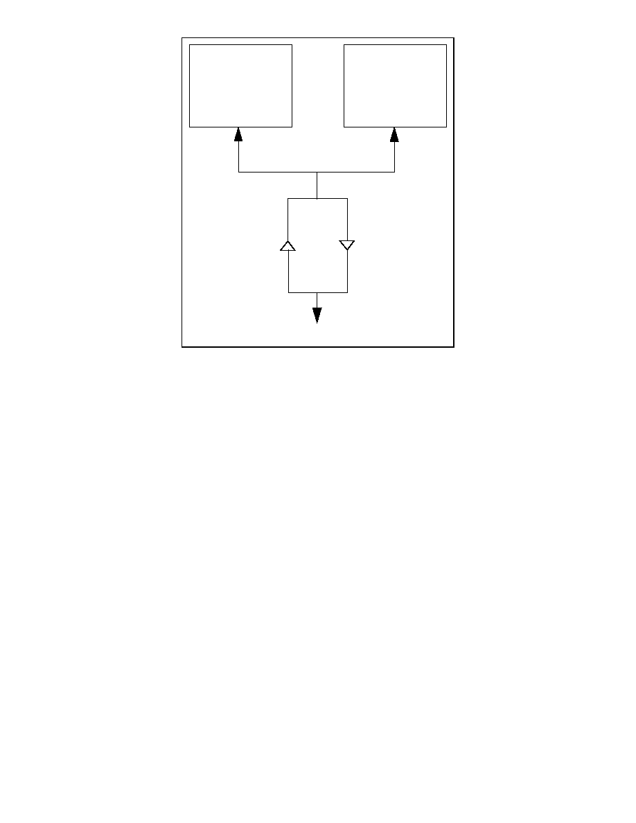
SMSC DS SLC90E66
Page 249
Rev. 07/10/2002
SMB
HOST
Controller
SMB Slave
Interface
- Host Slave
- Shadow Ports
SM Bus
FIGURE 28 - SYSTEM MANAGEMENT BUS CONTROLLER
11.6.1 SMBUS HOST INTERFACE
The SMBus Host Controller is used to send host commands to various SMBus devices. The SLC90E66 contains a
full host controller implemenatation. The SLC90E66 SMBus controller supports seven command protocols of the
SMBus interface (See System Management Bus Specification, Rev. 1.0):
§
Quick
Command
§
Send
Byte
§
Receive
Byte
§
Write
Byte/Word
§
Read
Byte/Word
§
Block
Read
§
Block
Write
To initiate a SMBus host transfer, the type of transfer protocol, the address of the SMBus device, the device specific
command, the data, and any control bits are first setup. Then the START bit is set, which triggers the host controller
to execute the transaction. Upon completion of the transaction, the SLC90E66 will generate an interrupt if enabled.
The interrupt can be selected either IRQ9 or nSMI. The system software can wait for interrupt to signal completion or
it can monitor the HOST_BUSY status bit. An interrupt will also be signaled if an error occurred during the transaction
or if the transaction was terminated by software setting the KILL bit. After setting the START bit while the
HOST_BUSY bit is Active, all host controller registers with names prefixed with "SMBHST" should not be accessed.
The SMBus controller will not respond to the START bit being set unless all interrupt status bits in the SMBHSTSTS
register have been cleared.
For Block Read or Block Write protocols, the data is stored in a 32-byte block data storage array. This array is
addressed via an internal index pointer. The index pointer is initialized to zero on each read of the SMBHSTCNT
register, and it is incremented by one after each access to the SMBBLKDAT register. For Block Write transactions,
the data to be transferred is stored in this array and the byte count is stored in SMBHSTDAT0 register before
initiating the transaction. For Block Read transactions, the SMBus peripheral decides the amount of data to be
transferred. After the transactions is completed, the byte count transferred is stored in the SMBHSTDAT0 register
and data is stored in the block data array.

SMSC DS SLC90E66
Page 250
Rev. 07/10/2002
Accesses to the data array during execution of the SMBus transaction always starts at address 0.
Any register values needed for later reference purpose should be saved before the starting of a new transaction, as
the SMBus host controller will update the registers while executing the new transaction.
11.6.2 SMBUS SLAVE INTERFACE
There are three mechanisms for SMBus peripherals to communicate to the SLC90E66. In addition to transferring
data, these mechanisms can generate an interrupt or resume the system from a suspend state. Once the slave
interface has received a transaction and generated an interrupt, it will stop responding to new requests until all the
interrupt status bits in the SMBSLVSTS register are cleared.
Mechanism 1: Access to Host Slave Port 10h
The first mechanism consists of accesses to the SMBus controller host slave port at address 10h. Note this address
is actually 0001 000x as this is a 7 bit address (bits [7-1] with bit 0 being R/W bit. The host slave port only responds
to Word Write transactions with the incoming data being stored in the SMBSLVDAT register and incoming command
in the SMBSHDWCMD register. An interrupt or resume event will be generated (if enabled) if the incoming command
matches the command stored in SMBSLVC register and at least one bit read into the register matches with the
corresponding bit in the SMBSLVEVT register.
Mechanism 2: Access to Slave Shadow Ports
The second mechanism monitors for accesses to the SMBus controller slave shadow ports at addresses stored in
SMBSHDW1 and SMBSHDW2 registers. The shadow slave ports also only responds to Word Write transactions with
the incoming data being stored in SMBSLVDAT register and incoming command being stored in the SMBSHDWCMD
register. An interrupt or resume event will be generated (if enabled) upon accesses to the slave shadow ports.
The SLV_BSY bit indicates that the SLC90E66 slave interface is receiving an incoming message. The SMBSLVCNT,
SMBSHDWCMD, SMBSLVENT, SMBSLVDAT and SMBSLVC registers should not be accessed while the SLV_BSY
bit is active (until completion of transaction).
Mechanism 3: nSMBALERT Assertion
The third method for SMBus devices to communicate with the SLC90E66 is through the nSMBALERT signal. When
enabled and the nSMBALERT signal is asserted, the SLC90E66 will generate an interrupt or resume the system from
a suspend state. This mechanism allows a device without SMBus master capabilities to request service from the
SMBus host. To determine which device asserted the nSMBALERT signal, the SLC90E66 host controller should be
programmed to execute a read command using the Alert Response Address.

SMSC DS SLC90E66
Page 251
Rev. 07/10/2002
12.0 PINOUT AND PACKAGE INFORMATION
The SLC90E66 uses a 324-ball Plastic Ball Grid Array (PBGA) package. The mechanical dimensions and the pinout
of the chip are outlined as follows.
12.1 SLC90E66 BGA Package Information
FIGURE 29 PACKAGE DIMENSIONS
D
Pin #1 I.D.
E1
E
D1
A
A1
TOP VIEW
SIDE VIEW
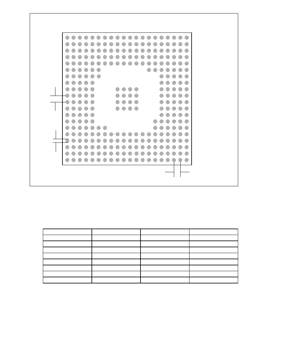
SMSC DS SLC90E66
Page 252
Rev. 07/10/2002
1
2 3 4 5 6 7 8 9 10 11 12 13 14 15 16 17 18 19 20
A
B
C
D
E
F
G
H
J
K
L
M
N
P
R
T
U
V
W
Y
FIGURE 30 SLC90E66 324-BALL BGA BALL PATTERN
SYMBOL
MIN (mm)
NOMINAL (mm)
MAX (mm)
A
2.16
2.36
2.56
A1
0.50
0.60
0.70
D
26.80
27.00
27.20
D1
23.90
24.00
24.10
E
26.80
27.00
27.20
E1
23.90
24.00
24.10
b
0.60
0.75
0.90
e
1.07
1.27
1.47
Pin #1
Corner
e
b
Top View
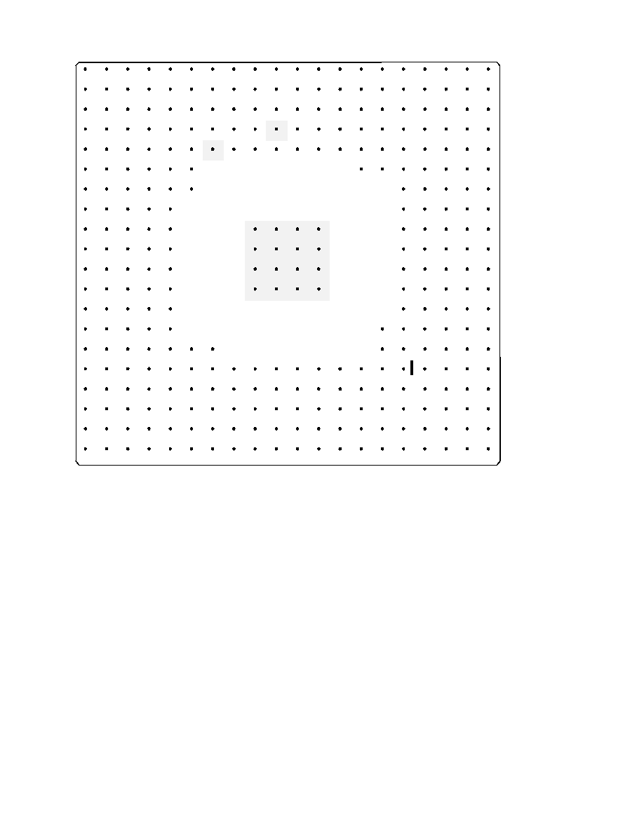
SMSC DS SLC90E66
Page 253
Rev. 07/10/2002
1
2
3
4
5
6
7
8
9
10 11 12 13 14 15 16 17 18 19 20
nPCIRST
AD27
IDSEL
AD19
nFRAME
nSERR
AD13
AD9
AD5
AD1
nPCI
REQB
nPHLDA
SDD6
SDD4
SDD13
SDDREQ nSDACK
SDA2
PDD8
PDD7
A
AD31
AD26
AD23
AD18
nIRDY
PAR
AD12
AD8
AD4
AD0
nPCI
REQC
nPHOLD
SDD9
SDD11
SDD1
nSDIOW
SDA1
nSDCS1
PDD9
PDD6
B
AD30
AD25
AD22
AD17
nTRDY
C/nBE1
AD11
C/nBE0
AD3
nCLK
RUN
nPCI
REQD
SDD7
SDD5
SDD3
SDD14
nSDIOR
SDA0
nSDCS3
PDD10
PDD5
C
AD28
C/nBE3
AD20
C/nBE2
nSTOP
AD14
AD10
AD6
AD2
VSS
PCICLK
SDD8
SDD10
SDD2
SDD15
SIORDY
PDD12
PDD3
PDD11
PDD4
D
AD29
AD24
AD21
AD16
nDEVSEL
AD15
VSS
AD7
VCC
nPCI
REQA
VCC
VCC
VSS
SDD12
SDD0
VCC
PDD14
PDD1
PDD13
PDD2
E
USBP1+
GPO28
GPO29
GPO30
VCC
VCC
VCC
VCC
nPDIOW
nPDIOR
PDREQ
PDD15
PDD0
F
nPIRQD
USBP0+
GPI21
GPO0
GPO27
VCC
PDA0
PDA2
PDA1
nPDACK
PIORDY
G
GPI18
USBP1-
USBP0-
GPI19
GPI20
nPDCS3
nPDCS1 nAPICCS nTHERM
IRQ0
H
nOC0
nOC1
GPI14
NC
VSS-USB
VSS
VSS
VSS
VSS
N.C.
NAPIC
ACK
nSTPCLK SERIRQ
IRQ1
J
nKBCS
nRTCCS
GPI16
GPI17
VCC-USB
VSS
VSS
VSS
VSS
ZZ
SPKR
NAPIC
REQ
nFERR
nSLP
K
RTCALE
GPI13
CLK48M
nPCS0
GPI15
VSS
VSS
VSS
VSS
VCC-RTC nIGNNE
INIT
INTR
NMI
L
nREQ_A nBIOSCS
nXDIR
nXOE
NC
VSS
VSS
VSS
VSS
XOSCSEL nRSMRST PWRGD CPURST
nA20M
M
nGNT_A
nREQ_B nPCBLID
nMCCS
nPCS1
VCC-SUS
nSMB
ALERT
nSCBLID
RTCX1
nRCIN
N
GATEA20 nGNT_B
nREQ_C nGNT_C
nPIRQC
VCC
LID
SUSCLK
nRI
nGPI1
nSMI
P
nCPU_
STP
nPCI_
STP
nPIRQA
nPIRQB
NC
VCC
VCC
VCC
VCC-SUS CONFIG1 CONFIG2 SMBCLK
RTCX2
R
SD6
SD3
IOCHRDY nIOWR
SA16
VCC
SYSCLK
SA9
IRQ3
SA4
SA1
LA23
IRQ12/M
LA18
nDACK5
SD9
nSUS_
STAT1
nSUS_
STAT2
GPO8
SMB
DATA
T
IRQ9
SD2
nSMWR
SA18
DREQ3
DREQ1
SA11
IRQ5
SA6
BALE
SA0
IRQ10
LA20
nDACK0
nMWR
DREQ6
DREQ7
nSUSC nBATLOW nPWRBT
N
U
SD7
DREQ2
SD0
SA19
nDACK3
SA14
SA12
IRQ6
SA7
TC
OSC
nIOCS16
LA21
IRQ14
nMRD
nDACK6
SD11
nTEST
nSUSB
nEXTSMI
V
RSTDRV
SD4
SD1
nSMRD
SA17
nDACK1 nREFRSH
SA10
IRQ4
SA5
SA2
nSBHE
IRQ11
LA19
DREQ0
SD8
nDACK7
SD13
SD15
nSUSA
W
nIOCHK
SD5
nZEROW
S
AEN
nIOR
SA15
SA13
IRQ7
SA8
nDACK2
SA3
nMEM
CS16
LA22
IRQ15
LA17
DREQ5
SD10
SD12
SD14
nIRQ8
Y
FIGURE 31 SLC90E66 PIN ASSIGNMENT

SMSC DS SLC90E66
Page 254
Rev. 07/10/2002
12.2 SLC90E66 Pin Assignment Tables in Alphabetical Order
Table 42 - SLC90E66 Pin Listing (Alphabetical)
SIGNAL
BALL NO.
SIGNAL
BALL NO.
SIGNAL
BALL NO.
A20GATE
P1
nCLKRUN
C10
nIOCHK
Y1
nA20M
M20
CONFIG1
R17
IOCHRDY
T3
AD0
B10
CONFIG2
R18
nIOCS16
V12
AD1
A10
CPURST
M19
nIOR
Y5
AD2
D9
nCPU_STP
R1
nIOW
T4
AD3
C9
nDACK0
U14
nIRDY
B5
AD4
B9
nDACK1
W6
IRQ0
H20
AD5
A9
nDACK2
Y10
IRQ1
J20
AD6
D8
nDACK3
V5
IRQ3
T9
AD7
E8
nDACK5
T15
IRQ4
W9
AD8
B8
nDACK6
V16
IRQ5
U8
AD9
A8
nDACK7
W17
IRQ6
V8
AD10
D7
nDEVSEL
E5
IRQ7
Y8
AD11
C7
DREQ0
W15
nIRQ8
Y20
AD12
B7
DREQ1
U6
IRQ9
U1
AD13
A7
DREQ2
V2
IRQ10
U12
AD14
D6
DREQ3
U5
IRQ11
W13
AD15
E6
DREQ5
Y16
IRQ12/M
T13
AD16
E4
DREQ6
U16
IRQ14
V14
AD17
C4
DREQ7
U17
IRQ15
Y14
AD18
B4
nEXTSMI
V20
nKBCCS
K1
AD19
A4
nFERR
K19
LA17
Y15
AD20
D3
nFRAME
A5
LA18
T14
AD21
E3
nGNTA
N1
LA19
W14
AD22
C3
nGNTB
P2
LA20
U13
AD23
B3
nGNTC
P4
LA21
V13
AD24
E2
nGPI1
P19
LA22
Y13
AD25
C2
GPI13
L2
LA23
T12
AD26
B2
GPI14
J3
LID
P16
AD27
A2
GPI15
L5
nMCCS
N4
AD28
D1
GPI16
K3
nMEMCS16
Y12
AD29
E1
GPI17
K4
nMEMR
V15
AD30
C1
GPI18
H1
nMEMW
U15
AD31
B1
GPI19
H4
AEN
Y4
GPI20
H5
nAPICACK
J17
GPI21
G3
nAPICCS
H18
GPO0
G4
nAPICREQ
K18
GPO8
T19
BALE
U10
GPO27
G5
nBATLOW
U19
GPO28
F2
nBIOSCS
M2
GPO29
F3
N.C.
J4
J16
M5
R5
C/nBE0
C8
GPO30
F4
NMI
L20
C/nBE1
C6
IDSEL
A3
nOC0
J1
C/nBE2
D4
nIGNNE
L17
nOC1
J2
C/nBE3
D2
INIT
L18
OSC
V11
CLK48
L3
INTR
L19
PAR
B6

SMSC DS SLC90E66
Page 255
Rev. 07/10/2002
SIGNAL
BALL NO.
SIGNAL
BALL NO.
SIGNAL
BALL NO.
nPCBLID
N3
nRI
P18
nSDCS3
C18
PCICLK
D11
nRSMRST
M17
SDD0
E15
nPCI_STP
R2
RSTDRV
W1
SDD1
B15
nPCIREQA
E10
RTCALE
L1
SDD2
D14
nPCIREQB
A11
nRTCCS
K2
SDD3
C14
nPCIREQC
B11
RTCX1
N19
SDD4
A14
nPCIREQD
C11
RTCX2
R20
SDD5
C13
nPCIRST
A1
SA0
U11
SDD6
A13
nPCS0
L4
SA1
T11
SDD7
C12
nPCS1
N5
SA2
W11
SDD8
D12
PDA0
G16
SA3
Y11
SDD9
B13
PDA1
G18
SA4
T10
SDD10
D13
PDA2
G17
SA5
W10
SDD11
B14
nPDCS1
H17
SA6
U9
SDD12
E14
nPDCS3
H16
SA7
V9
SDD13
A15
PDD0
F20
SA8
Y9
SDD14
C15
PDD1
E18
SA9
T8
SDD15
D15
PDD2
E20
SA10
W8
nSDDACK
A17
PDD3
D18
SA11
U7
SDDREQ
A16
PDD4
D20
SA12
V7
nSDIOR
C16
PDD5
C20
SA13
Y7
nSDIOW
B16
PDD6
B20
SA14
V6
SERIRQ
J19
PDD7
A20
SA15
Y6
nSERR
A6
PDD8
A19
SA16
T5
SIORDY
D16
PDD9
B19
SA17
W5
nSLP
K20
PDD10
C19
SA18
U4
nSMBALERT
N17
PDD11
D19
SA19
V4
SMBCLK
R19
PDD12
D17
nSBHE
W12
SMBDATA
T20
PDD13
E19
nSCBLID
N18
nSMEMR
W4
PDD14
E17
SD0
V3
nSMEMW
U3
PDD15
F19
SD1
W3
nSMI
P20
nPDDACK
G19
SD10
Y17
SPKR
K17
PDDREQ
F18
SD11
V17
nSTOP
D5
nPDIOR
F17
SD12
Y18
nSTPCLK
J18
nPDIOW
F16
SD13
W18
nSUS_STAT1
T17
nPHLDA
A12
SD14
Y19
nSUS_STAT2
T18
nPHOLD
B12
SD15
W19
nSUSA
W20
PIORDY
G20
SD2
U2
nSUSB
V19
nPIRQA
R3
SD3
T2
nSUSC
U18
nPIRQB
R4
SD4
W2
SUSCLK
P17
nPIRQC
P5
SD5
Y2
SYSCLK
T7
nPIRQD
G1
SD6
T1
TC
V10
POWEROK
M18
SD7
V1
nTEST
V18
nPWRBTN
U20
SD8
W16
nTHRM
H19
nRCIN
N20
SD9
T16
nTRDY
C5
nREFRESH
W7
SDA0
C17
USBP0-
H3
nREQA
M1
SDA1
B17
USBP0+
G2
nREQB
N2
SDA2
A18
USBP1-
H2
nREQC
P3
nSDCS1
B18
USBP1+
F1

SMSC DS SLC90E66
Page 256
Rev. 07/10/2002
SIGNAL
BALL NO.
SIGNAL
BALL NO.
SIGNAL
BALL NO.
VSS
M11
M12
VSS-USB
J5
nXDIR
M3
nXOE
M4
XOSCSEL
M16
nZEROWS
Y3
ZZ
K16
VCC
E9
E11
E12
E16
F5
F6
F14
F15
G6
P15
R6
R7
R15
T6
VCC-RTC
L16
VSS
E13
J9
J10
J11
J12
K9
K10
K11
K12
L9
L10
L11
L12
M9
M10
VCC-SUS
N16
R16
VSS
D10
E7
VCC-USB
K5

SMSC DS SLC90E66
Page 257
Rev. 07/10/2002
13.0 SLC90E66
REVISIONS
PAGE(S)
SECTION/FIGURE/ENTRY
CORRECTION
DATE REVISED
1
Features
First bullet on features
list
Changed from:
"Enhanced PCI South
Bridge for Desktop and
Mobile Applications"
Changed to:
"Enhanced PCI South
Bridge for Desktop,
Mobile
and
Embedded
Applications"
07/10/02
1
Features
First sub-bullet in the left
column on features list
Changed from:
"Pin and Register
Compatible with Intel
82371EB PIIX4E South
Bridge"
Changed to:
"
Pin Compatible
with
Intel 82371EB PIIX4E
South Bridge"
07/10/02
254
Table 42 - SLC90E66 Pin
Listing (Alphabetical)
Ball #M16 removed
under N.C. signal
01/18/01