
1
QuickLogic QL80FC Programmable Fibre Channel ENDEC
QL80FC - QuickFC
TM
Rev A
QL80FC - QuickFC
Features
I
ANSI Fibre Channel (FC) compatibility
I
Data rates up to 2.5 Gb/s supported
I
2.5Gb/s Simplex (200 MByte/s) or Duplex
(400 MByte/s) Mode
I
Compatible with standard SERDES components
I
32 bit synchronous FIFO system interface
I
Tx and Rx internal FIFO for system applications
without external FIFOs
I
Selectable 20-bit/10-bit encoded transmission
character interface to SERDES
I
8b/10b Encoding/Decoding
I
CRC Calculation and checking per FC standard
I
Fibre Channel Loss of Synchronization (LOS) state
machine
I
Support for arbitrated loops
I
IntraFrame idles support for proprietary links
I
"Raw" data path for the injection of encoding and
CRC errors into the bitsteam for use in testing link
error handling functions
I
3.3V operating voltage
I
3.3V CMOS I/O, 5.0V CMOS tolerant inputs
I
208 PQFP and 456 PBGA packages available
Extended Features
Extended features that can be designed into the user
customizable logic:
I
Fibre Channel Link Control State Machine (LCSM)
I
RRDY credit management for link flow control
I
Microprocessor interface to configure various link
modes
I
BIST functions support link bit error rate
measurements
F
EATURES
E
XTENDED
F
EATURES
Dual Port SRAM
I
22 blocks (total of 25,344 bits) of dual-port RAM
I
Configurable as RAM, ROM or FIFO
I
Can be configured as two internal FIFOs of up to
352 x 36 in size
I
Configurable RAM array sizes (by 2, 4, 9, 18)
I
<5ns access times, 160+Mhz FIFOs
High Speed Customizable Logic
I
Up to 269 customizable I/O pins
I
751 Logic cells
I
300 MHz 16-bit counters, 400 MHz Data paths
I
Mux-Based architecture; non-volatile technology
I
Completely customizable for any digital application
Fibre Channel Block Diagram
D
UAL
P
ORT
SRAM
H
IGH
S
PEED
C
USTOMIZABLE
L
OGIC
RAM Blocks
22 Blocks (25K bits)
IO
P
i
n
s
Fibre Channel ENDEC
Customizable
Logic Cells
IO
P
i
n
s
Transmit
Receive
10 bit/20 bit
10 bit/20 bit
IO Pins

2
Preliminary
2
QL80FC - QuickFC
TM
FIGURE 1. System Level Diagram
General Description
The QL80FC device in the QuickLogic QuickFC ESP
(Embedded Standard Product) family provides a com-
pletely integrated configurable Fibre Channel
Encoder/Decoder interface solution combined with
customizable logic. This device provides a means to
receive and transmit high-speed serial data and
implement a Fibre Channel Link interface or any
proprietary high-speed serial link.
The chip is divided into two main portions, an
embedded design and a customizable design. The
embedded design contains the built in functionality of
Fibre Channel's FC-1 and FC-2 layers, which the sys-
tem designer uses as a standard product. This portion
can not be modified. As such, all functionality and
timing requirements have been verified in hardware
and are guaranteed.
The customizable portion consists of user customiz-
able system gates, and interfaces directly to the
embedded portion of the chip. These gates may be
programmed to implement glue logic to other bus
standards such as PCI or SCSI. They can also be pro-
grammed with Fibre Channel Upper Layer Protocols.
Of course, the designer may choose to modify Upper
Layer Protocols for customization. In this way, the
QuickLogic QL80FC provides the embedded systems
designer with an easy to use and cost effective solu-
tion for embedded serial applications.
Fibre Channel Application
The QL80FC ENDEC is a high performance
encoder/decoder designed for use in conjunction
with Gb/s SERDES transmitter/receiver chips. These
chips, when combined with internal FIFO buffer
memory, can be used to build a complete serial link.
Optional, external FIFOs can be used in place of the
available internal FIFOs to extend buffering to sizes
beyond 352 words.
The embedded ENDEC is a full duplex design with an
encoder section for transmission and a decoder sec-
tion for reception. The transmitter/encoder section
accepts a 4-byte user data word, encodes each byte
into a 10-bit transmission character and outputs
transmission characters to the SERDES transmitter.
This equals two 10-bit characters per clock (one 10-
bit character per clock in 10-bit mode). The receiver/
decoder section accepts two 10-bit transmission char-
System
Bus
(Optional)
Transmit
FIFO
(Optional)
Receive
FIFO
FIFO Control
User Customizable
Logic
Embedded
Fibre Channel
ENDEC
QL80FC Programmable ENDEC Chip
Bridge Logic
For Data Path
Transmit/
Receive
SERDES
2.5 Gb/s Serial
Data Over
Copper or
Optical Cable
Internal
Transmit
FIFO
Internal
Receive
FIFO
Micro-Processor
Or
System Bus
Interface
G
ENERAL
D
ESCRIPTION
F
IBRE
C
HANNEL
A
PPLICATIONS

3
QL80FC - QuickFC
TM
acters from the SERDES receiver (one 10-bit charac-
ter in 10-bit mode), decodes them, and outputs a 4-
byte user data word.
The QL80FC has a system interface that emulates a
synchronous FIFO for ease of use. FIFOs allow maxi-
mum sustained performance of 400 MB/s running a
full duplex link. Their function is to handle the asyn-
chronous interface between the bus data rate and the
different serial data rates, and handle phase and fre-
quency differences inherent in serial links. Internal
FIFOs of 352 x 36 or external FIFOs can be used to
expand the buffering to accommodate multiple
frames.
The QL80FC includes the hardware necessary for
packetized data protection. Framing functions are
provided via Fibre Channel compliant command
words (ordered sets) for Start of Frame and End of
Frame. CRC generation and data frame verification
protect the Fibre Channel frame header and data
field when these framing functions are used.
The device provides a microprocessor interface that
allows the user to manage the serial link. Signals are
also provided to decode serial link error conditions
and differentiate between data and commands. The
QL80FC implements link synchronization with the
SERDES chip through the Loss of Synchronization
State Machine (LOS) as required by the ANSI FC-PH
specification. The LOS manages receiver word syn-
chronization with the RxComDet (comma detect) sig-
nal.
The QL80FC is a versatile part that allows the system
designer to create proprietary or Fibre Channel com-
pliant serial links by taking advantage of some, or all,
of the Fiber Channel compliant features. It has a
number of useful features for system designers of
proprietary links. One such feature is the ability to
send intraframe IDLEs. These characters are auto-
matically sent if the FIFO is empty, but they do not
affect the CRC. In this mode the QL80FC allows
simple interfacing to systems where the flow of data
may be interrupted.
Embedded Design Functional Description
The embedded FC-1 and FC-2 layers are divided into
two functional groupings: the Transmit data path and
the Receive data path. A functional diagram for the
Transmit path is included in Figure 2.
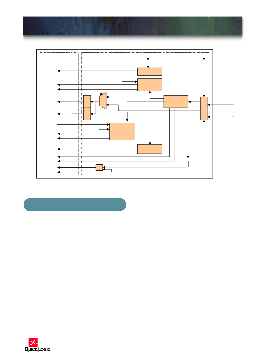
FIGURE 2. Customizable ENDEC Chip Functional Block Diagram - Transmit and LCSM Data Paths
E
MBEDDED
D
ESIGN
F
UNCTIONAL
D
ESCRIPTION
CRC Generation
8b/10b Encoder
User Programmable
Logic
TxData[31:0]
Embedded Fibre Channel ENDEC
Re
gi
s
t
e
r
s
TxCrcEn
Re
gi
s
t
e
r
s
TxRawEn
TxOut[19:0]
TxClk125_in
TxClk125_out
TxClk63
/2
TxRst
To receive data path
TxKChar
Async_rst
TenbMode
Re
g
i
s
t
e
r
s
TxRData[39:32]
Async_rst
TenbMode
TxIFIdleEn
(only [9:0] used
in 10b mode)
TxClk63 Sync
Reset Circuit
Clk_rst
Clk_rst
To receive data path

4
Preliminary
4
QL80FC - QuickFC
TM
Transmit Data Path
When the transmit data path is in standard operation
(TxRawEn not asserted) the chip will latch an un-
encoded, Fibre Channel, 32-bit word on inputs
TxData[31:0]. This data then passes on to the 8b/
10b encoder, which creates a 40-bit encoded Fibre
Channel word. The encoder will encode the most sig-
nificant character as a command character if the
TxKChar input line is asserted. This word is regis-
tered and passed to the SERDES in 20-bit chunks (10
bit chunks if 10 bit mode is enabled) on the TxOut
signal lines.
Asserting the TxCrcEn signal enables the CRC Gen-
eration block. This block will automatically detect the
SOF ordered set and begin CRC generation using the
ANSI specified CRC polynomial. It will continue until
an EOF or any other FC ordered set is encountered
(unless TxIFIdleEn is asserted, then the IDLE ordered
set will be ignored by the CRC generator). It then
inserts the CRC value into the data path for transmis-
sion to the SERDES.
The TxRawEn signal enables the raw transmit data
path when asserted. In this mode, the 8 bits of TxR-
Data is concatenated onto the 32 bits of the TxData
signal to create a 40-bit wide data path. The CRC
generation and 8b/10b encoder blocks are bypassed
and the "raw" data latched at the inputs is passed
directly to the output registers that drive the SER-
DES. This mode is useful for testing the error han-
dling capabilities of the serial link by providing the
systems designer a way to intentionally introduce
errors into the serial bit stream.
The TxIFIdleEn (Intra-Frame Idle Enable) input
enables the use of Fibre Channel IDLE words within
a Frame. When this signal is asserted, IDLE words
present within a data frame will not affect the value
generated by the CRC block. This feature is useful in
custom FC designs where it is desired to suspend the
transmission of a frame for a period of time and then
resume later.
The use of external FIFOs is optional. There is
enough RAM on the ENDEC chip to be configured
into two 352 x 36 FIFOs. If FIFOs of this size are all
that is required, external FIFOs would not be needed.
Synchronous read and writes directly from the system
bus without a FIFO is also possible.
Two clock signals are supplied to the customizable
logic on high speed, low skew clock networks:
TxClk125 and TxClk63. TxClk125 is a clock run-
ning at a maximum speed of 125 MHz, and repre-
sents the "full speed" of the Oscillator being used to
clock the transmit data path. The input that drives
this signal is also used to clock the SERDES chip.
The TxClk63 clock signal operates at half the speed
of the TxClk125 clock. You will most likely want to
use the TxClk63 signal to clock your FIFOs and cus-
tomizable logic. Of course, these signals can be
routed off-chip through the customizable I/O.
The Async_rst pin accepts an asynchronous, active
high reset signal. Circuitry takes this signal and syn-
chronizes it with the TxClk63 clock. This synchro-
nous reset signal, TxRst, is used to set or clear flip-
flops in the transmit data path. It is made available to
the user programmable logic for the same purpose
on a high speed, low skew network
The Clk_rst input stops the TxClk63 clock when this
signal is asserted. This signal was added primarily to
facilitate simulation. Clk_rst may be permanently
grounded in hardware.
T
RANSMIT
D
ATA
P
ATH
5
QL80FC - QuickFC
TM
FIGURE 3.
.
Customizable ENDEC Chip Functional Block Diagram - Receive Data Path
Receive Data Path
Receive Data Path
The receive data path receives encoded data from an
on-board SERDES, decodes it and passes the result-
ing data to the customizable section of the chip. A
functional block diagram of the receive data path is
shown in Figure 3.
The RxClk125 signal latches 20 bits (10 bits when
10-bit mode is enabled) of data from the SERDES
into the RxIn input registers on the positive edge of
the clock. The RxClk125 signal is made available to
the customizable section. RxClk125 is divided by two
and made available to the customizable section on
the RxClk63 signal line. Both clocks use a high
speed, low skew clock network. Again you will most
likely want to use the RxClk63 signal to clock all reg-
isters and FIFOs in the receive data path. Registers
using RxClk125 and RxClk63 should be sensitive to
the rising edge of these clocks.
Once the data on the RxIn signal lines is latched into
the input registers, the data is passed on to the 8b/
10b decoder. Under standard operation, (input RxRa-
wEn is low), the data is decoded into 4, 8-bit charac-
ters and the resulting Fibre Channel word is placed
on the RxData[31:0] output signals. RxRData is not
used under normal operation. If the decoder detects a
Fibre Channel comma character in the most signifi-
cant character of the word, the RxKChar signal line
will be asserted.
When the RxCrcEn signal is asserted the CRC check-
ing logic will function. The CRC logic will automati-
cally detect a SOF word and begin performing CRC
division on the next word in the data stream using the
ANSI specified CRC polynomial for Fibre Channel.
When an EOF word or any other FC ordered set is
detected (unless RxIFIdleEn is asserted, then the IDLE
ordered set will be ignored by the CRC checker) the
CRC will assert the RxCrcRdy signal for one cycle of
the RxClk63 clock. If the remainder for the division is
zero, the RxCrcOK signal line will also be asserted
during this same cycle.
User Programmable
Logic
Embedded Fibre Channel ENDEC
RxClk125_in
RxClk125_out
RxClk63
/2
8b/10b Decoder
Loss Of Sync
State Machine
CRC Checking
Ordered Set
Recognition
Re
gis
t
e
r
s
RxIn[19:0]
RxComDet
RxLOSync
RxLOSIdx[3:0]
RxData[31:0]
Regis
t
e
r
s
RxRawEn
RxKChar
RxCrcOK
RxCrcRdy
(SOF, IDLE, EOF . . . )
RxSgpBus[14:0]
From transmit data path
Async_rst
RxCrcEn
(only [9:0] used
in 10b mode)
Re
gis
t
e
r
s
RxRData[39:32]
TenbMode
RxInvW ord
RxIFIdleEn
RxClk63 Sync
Reset Circuit
RxRst
Clk_rst
From transmit
data path
R
ECEIVE
D
ATA
P
ATH