TISP4240F3, TISP4260F3, TISP4290F3, TISP4320F3, TISP4380F3
SYMMETRICAL TRANSIENT
VOLTAGE SUPPRESSORS
P R O D U C T I N F O R M A T I O N
1
MARCH 1994 - REVISED SEPTEMBER 1997
Copyright © 1997, Power Innovations Limited, UK
Information is current as of publication date. Products conform to specifications in accordance
with the terms of Power Innovations standard warranty. Production processing does not
necessarily include testing of all parameters.
TELECOMMUNICATION SYSTEM SECONDARY PROTECTION
q
Ion-Implanted Breakdown Region
Precise and Stable Voltage
Low Voltage Overshoot under Surge
q
Planar Passivated Junctions
Low Off-State Current
< 10 µA
q
Rated for International Surge Wave Shapes
q
Surface Mount and Through-Hole Options
q
UL Recognized, E132482
description
These high voltage symmetrical transient voltage
suppressor devices are designed to protect two
wire telecommunication applications against
transients caused by lightning strikes and a.c.
power lines. Offered in five voltage variants to
meet battery and protection requirements they
are guaranteed to suppress and withstand the
listed international lightning surges in both
polarities.
Transients are initially clipped by breakdown
clamping until the voltage rises to the breakover
DEVICE
V
DRM
V
V
(BO)
V
`4240F3
180
240
`4260F3
200
260
`4290F3
220
290
`4320F3
240
320
`4380F3
270
380
WAVE SHAPE
STANDARD
I
TSP
A
2/10 µs
FCC Part 68
175
8/20 µs
ANSI C62.41
120
10/160 µs
FCC Part 68
60
10/560 µs
FCC Part 68
45
0.5/700 µs
RLM 88
38
10/700 µs
FTZ R12
VDE 0433
CCITT IX K17/K20
50
50
50
10/1000 µs
REA PE-60
35
PACKAGE
PART # SUFFIX
Small-outline
D
Small-outline taped
and reeled
DR
Single-in-line
SL
level, which causes the device to crowbar. The
high crowbar holding current prevents d.c.
latchup as the current subsides.
These monolithic protection devices are
fabricated in ion-implanted planar structures to
ensure precise and matched breakover control
and are virtually transparent to the system in
normal operation
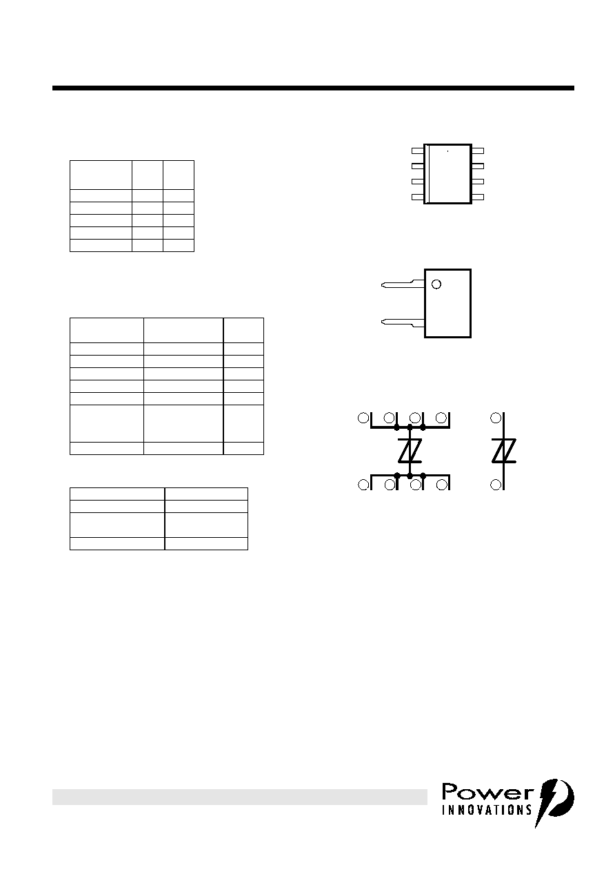
The small-outline 8-pin assignment has been
carefully chosen for the TISP series to maximise
the inter-pin clearance and creepage distances
which are used by standards (e.g. IEC950) to
establish voltage withstand ratings.
device symbol
T
SD4XAE
Terminals T and R correspond to the
alternative line designators of A and B
R
R
R
R
T
T
T
1
2
3
4
5
6
7
8
T
R
D PACKAGE
SL PACKAGE
1
2
D PACKAGE
(TOP VIEW)
SL PACKAGE
(TOP VIEW)
MDXXAI
1
2
3
4
5
6
7
8
R
R
R
R
T
T
T
T
Specified ratings require the connection
of pins 1, 2, 3 and 4 for the T terminal.
1
2
T
R
MDXXAH
MD4XAA

TISP4240F3, TISP4260F3, TISP4290F3, TISP4320F3, TISP4380F3
SYMMETRICAL TRANSIENT
VOLTAGE SUPPRESSORS
2
MARCH 1994 - REVISED SEPTEMBER 1997
P R O D U C T I N F O R M A T I O N
absolute maximum ratings
NOTES: 1. Further details on surge wave shapes are contained in the Applications Information section.
2. Initially the TISP must be in thermal equilibrium with 0°C < T
J
<70°C. The surge may be repeated after the TISP returns to its initial
conditions.
3. Above 70°C, derate linearly to zero at 150°C lead temperature.
NOTE
4: Further details on capacitance are given in the Applications Information section.
RATING
SYMBOL
VALUE
UNIT
Repetitive peak off-state voltage (0°C < T
J
< 70°C)
`4240F3
`4260F3
`4290F3
`4320F3
`4380F3
V
DRM
± 180
± 200
± 220
± 240
± 270
V
Non-repetitive peak on-state pulse current (see Notes 1, 2 and 3)
I
TSP
A
1/2 µs (Gas tube differential transient, open-circuit voltage wave shape 1/2 µs)
350
2/10 µs (FCC Part 68, open-circuit voltage wave shape 2/10 µs)
175
8/20 µs (ANSI C62.41, open-circuit voltage wave shape 1.2/50 µs)
120
10/160 µs (FCC Part 68, open-circuit voltage wave shape 10/160 µs)
60
5/200 µs (VDE 0433, open-circuit voltage wave shape 2 kV, 10/700 µs)
50
0.2/310 µs (RLM 88, open-circuit voltage wave shape 1.5 kV, 0.5/700 µs)
38
5/310 µs (CCITT IX K17/K20, open-circuit voltage wave shape 2 kV, 10/700 µs)
50
5/310 µs (FTZ R12, open-circuit voltage wave shape 2 kV, 10/700 µs)
50
10/560 µs (FCC Part 68, open-circuit voltage wave shape 10/560 µs)
45
10/1000 µs (REA PE-60, open-circuit voltage wave shape 10/1000 µs)
35
Non-repetitive peak on-state current (see Notes 2 and 3)
D Package
I
TSM
4
A rms
50 Hz,
1 s
SL Package
6
Initial rate of rise of on-state current,
Linear current ramp, Maximum ramp value < 38 A
di
T
/dt
250
A/µs
Junction temperature
T
J
-40 to +150
°C
Storage temperature range
T
stg
-40 to +150
°C
electrical characteristics for the T and R terminals, T
J
= 25°C
PARAMETER
TEST CONDITIONS
TISP4240F3
TISP4260F3
UNIT
MIN
TYP
MAX
MIN
TYP
MAX
I
DRM
Repetitive peak off-
state current
V
D
= ±V
DRM
, 0°C < T
J
< 70°C
±10
±10
µA
V
(BO)
Breakover voltage
dv/dt = ±250 V/ms,
R
SOURCE
= 300
±240
±260
V
V
(BO)
Impulse breakover volt-
age
dv/dt = ±1000 V/µs,
R
SOURCE
= 50
,
di/dt < 20 A/µs
±267
±287
V
I
(BO)
Breakover current
dv/dt = ±250 V/ms,
R
SOURCE
= 300
±0.15
±0.6
±0.15
±0.6
A
V
T
On-state voltage
I
T
= ±5 A,
t
W
= 100 µs
±3
±3
V
I
H
Holding current
di/dt = +/-30 mA/ms
±0.15
±0.15
A
dv/dt
Critical rate of rise of
off-state voltage
Linear voltage ramp
Maximum ramp value < 0.85V
(BR)MIN
±5
±5
kV/µs
I
D
Off-state current
V
D
= ±50 V
±10
±10
µA
C
off
Off-state capacitance
f = 100 kHz,
V
d
= 100 mV
(see Note 4)
V
D
= 0,
57
95
57
95
pF
V
D
= -5 V
26
45
26
45
pF
V
D
= -50 V
11
20
11
20
pF
3
MARCH 1994 - REVISED SEPTEMBER 1997
TISP4240F3, TISP4260F3, TISP4290F3, TISP4320F3, TISP4380F3
SYMMETRICAL TRANSIENT
VOLTAGE SUPPRESSORS
P R O D U C T I N F O R M A T I O N
NOTE
5: Further details on capacitance are given in the Applications Information section.
NOTE
6: Further details on capacitance are given in the Applications Information section.
electrical characteristics for the T and R terminals, T
J
= 25°C
PARAMETER
TEST CONDITIONS
TISP4290F3
TISP4320F3
UNIT
MIN
TYP
MAX
MIN
TYP
MAX
I
DRM
Repetitive peak off-
state current
V
D
= ±V
DRM
, 0°C < T
J
< 70°C
±10
±10
µA
V
(BO)
Breakover voltage
dv/dt = ±250 V/ms,
R
SOURCE
= 300
±290
±320
V
V
(BO)
Impulse breakover volt-
age
dv/dt = ±1000 V/µs,
R
SOURCE
= 50
,
di/dt < 20 A/µs
±317
±347
V
I
(BO)
Breakover current
dv/dt = ±250 V/ms,
R
SOURCE
= 300
±0.15
±0.6
±0.15
±0.6
A
V
T
On-state voltage
I
T
= ±5 A,
t
W
= 100 µs
±3
±3
V
I
H
Holding current
di/dt = +/-30 mA/ms
±0.15
±0.15
dv/dt
Critical rate of rise of
off-state voltage
Linear voltage ramp
Maximum ramp value < 0.85V
(BR)MIN
±5
±5
kV/µs
I
D
Off-state current
V
D
= ±50 V
±10
±10
µA
C
off
Off-state capacitance
f = 100 kHz,
V
d
= 100 mV
(see Note 5)
V
D
= 0,
57
95
57
95
pF
V
D
= -5 V
26
45
26
45
pF
V
D
= -50 V
11
20
11
20
pF
electrical characteristics for the T and R terminals, T
J
= 25°C
PARAMETER
TEST CONDITIONS
TISP4380F3
UNIT
MIN
TYP
MAX
I
DRM
Repetitive peak off-
state current
V
D
= ±V
DRM
, 0°C < T
J
< 70°C
±10
µA
V
(BO)
Breakover voltage
dv/dt = ±250 V/ms,
R
SOURCE
= 300
±380
V
V
(BO)
Impulse breakover volt-
age
dv/dt = ±1000 V/µs,
R
SOURCE
= 50
,
di/dt < 20 A/µs
±407
V
I
(BO)
Breakover current
dv/dt = ±250 V/ms,
R
SOURCE
= 300
±0.15
±0.6
A
V
T
On-state voltage
I
T
= ±5 A,
t
W
= 100 µs
±3
V
I
H
Holding current
di/dt = +/-30 mA/ms
±0.15
A
dv/dt
Critical rate of rise of
off-state voltage
Linear voltage ramp
Maximum ramp value < 0.85V
(BR)MIN
±5
kV/µs
I
D
Off-state current
V
D
= ±50 V
±10
µA
C
off
Off-state capacitance
f = 100 kHz,
V
d
= 100 mV
(see Note 6)
V
D
= 0,
57
95
pF
V
D
= -5 V
26
45
pF
V
D
= -50 V
11
20
pF
thermal characteristics
PARAMETER
TEST CONDITIONS
MIN
TYP
MAX
UNIT
R
JA
Junction to free air thermal resistance
P
tot
= 0.8 W, T
A
= 25°C
5 cm
2
, FR4 PCB
D Package
160
°C/W
SL Package
105

TISP4240F3, TISP4260F3, TISP4290F3, TISP4320F3, TISP4380F3
SYMMETRICAL TRANSIENT
VOLTAGE SUPPRESSORS
4
MARCH 1994 - REVISED SEPTEMBER 1997
P R O D U C T I N F O R M A T I O N
PARAMETER MEASUREMENT INFORMATION
Figure 1. VOLTAGE-CURRENT CHARACTERISTIC FOR T AND R TERMINALS
ALL MEASUREMENTS ARE REFERENCED TO THE R TERMINAL
-v
I
(BR)
V
(BR)
V
(BR)M
V
DRM
I
DRM
V
D
I
H
I
T
V
T
I
TSM
I
TSP
V
(BO)
I
(BO)
I
D
Quadrant I
Switching
Characteristic
+v
+i
V
(BO)
I
(BO)
I
(BR)
V
(BR)
V
(BR)M
V
DRM
I
DRM
V
D
I
D
I
H
I
T
V
T
I
TSM
I
TSP
-i
Quadrant III
Switching
Characteristic
PMXXAA

5
MARCH 1994 - REVISED SEPTEMBER 1997
TISP4240F3, TISP4260F3, TISP4290F3, TISP4320F3, TISP4380F3
SYMMETRICAL TRANSIENT
VOLTAGE SUPPRESSORS
P R O D U C T I N F O R M A T I O N
TYPICAL CHARACTERISTICS
R and T terminals
Figure 2.
Figure 3.
Figure 4.
Figure 5.
OFF-STATE CURRENT
T
J
- Junction Temperature - °C
-25
0
25
50
75
100
125
150
I
D
-
O
f
f
-
S
t
a
t
e
C
u
r
r
e
n
t
-
µ
A
0·001
0·01
0·1
1
10
100
TC3HAF
vs
V
D
= -50 V
V
D
= 50 V
JUNCTION TEMPERATURE
NORMALISED BREAKDOWN VOLTAGES
T
J
- Junction Temperature - °C
-25
0
25
50
75
100
125
150
N
o
r
m
a
l
i
s
e
d
B
r
e
a
k
d
o
w
n
V
o
l
t
a
g
e
s
0.9
1.0
1.1
1.2
TC3HAI
JUNCTION TEMPERATURE
vs
V
(BO)
V
(BR)
V
(BR)M
Positive Polarity
Normalised to V
(BR)
I
(BR)
= 100 µA and 25°C
NORMALISED BREAKDOWN VOLTAGES
T
J
- Junction Temperature - °C
-25
0
25
50
75
100
125
150
N
o
r
m
a
l
i
s
e
d
B
r
e
a
k
d
o
w
n
V
o
l
t
a
g
e
s
0.9
1.0
1.1
1.2
TC3HAJ
JUNCTION TEMPERATURE
vs
V
(BO)
V
(BR)
V
(BR)M
Negative Polarity
Normalised to V
(BR)
I
(BR)
= 100 µA and 25°C
ON-STATE CURRENT
V
T
- On-State Voltage - V
2
3
4
5
6
7 8 9
1
10
I
T
-
O
n
-
S
t
a
t
e
C
u
r
r
e
n
t
-
A
1
10
100
TC3HAL
ON-STATE VOLTAGE
vs
-40°C
150°C
25°C