
7EL2
BIDIRECTIONAL THYRISTOR OVERVOLTAGE PROTECTORS
P R O D U C T I N F O R M A T I O N
1
JANUARY 1999
Copyright © 1999, Power Innovations Limited, UK
Information is current as of publication date. Products conform to specifications in accordance
with the terms of Power Innovations standard warranty. Production processing does not
necessarily include testing of all parameters.
Manufactured by TI using silicon designed and manufactured by Power Innovations, Bedford, UK.
TELECOMMUNICATION SYSTEM PRIMARY PROTECTION
device symbol
T
R
SD4XAA
Terminals T and R correspond to the
alternative line designators of A and B
T(A)
R(B)
CELL PACKAGE
(SIDE VIEW)
MD4XACA
q
Ion-Implanted Breakdown Region
Precise and Stable Voltage
Low Voltage Overshoot under Surge
q
Rated for International Surge Wave Shapes
q
Gas Discharge Tube (GDT) Replacement
q
Planar Passivated Junctions in a Protected
Cell Construction
Low Off-State Current
DEVICE
V
(BR)
MINIMUM
V
V
(BO)
MINIMUM
V
V
(BO)
MAXIMUM
V
7EL2
±245
±265
±400
DEVICE
ITU-T K28
(10/700)
GR-974-CORE
(10/1000)
I
TSP
A
I
TSP
A
7EL2
±400
±300
Extended Service Life
q
Soldered Copper Electrodes
High Current Capability
Cell Construction Short Circuits Under Excessive Current Conditions
description
These devices are primary protector components for semiconductor arrester assemblies intended to meet the
generic requirements of Bellcore GR-974-CORE (November 1994) or ITU-T Recommendation K28 (03/93).
To conform to the specified environmental requirements, the 7EL2 must be installed in a housing which
maintains a stable microclimate during these tests.
The protector consists of a symmetrical voltage-triggered bidirectional thyristor. Overvoltages are initially
clipped by breakdown clamping until the voltage rises to the breakover level, which causes the device to
crowbar into a low-voltage on state. This low-voltage on state causes the current resulting from the
overvoltage to be safely diverted through the device. The high crowbar holding current prevents d.c. latchup
as the diverted current subsides. The 7EL2 is guaranteed to voltage limit and withstand the listed
international lightning surges in both polarities.
These monolithic protection devices are constructed using two nickel plated copper electrodes soldered to
each side of the silicon chip. This packaging approach allows heat to be removed from both sides of the
silicon, resulting in the doubling of the devices thermal capacity, enabling a power line cross current capability
of 10 A rms for 1 second. One of the 7EL2's copper electrodes is specially shaped to promote a progressive
shorting action (at 50/60 Hz currents greater than 60 A). The assembly must hold the 7EL2 in compression,
so that the cell electrodes can be forced together during overstress testing. Under excessive power line cross
conditions the 7EL2 will fail short circuit, providing maximum protection to the equipment.
7EL2
BIDIRECTIONAL THYRISTOR OVERVOLTAGE PROTECTORS
2
JANUARY 1999
P R O D U C T I N F O R M A T I O N
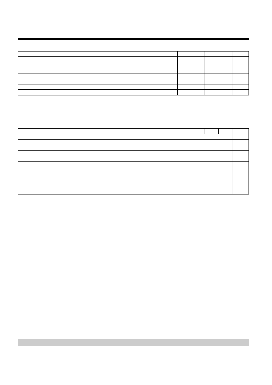
absolute maximum ratings, T
A
= 25°C (unless otherwise noted)
RATING
SYMBOL
VALUE
UNIT
Non-repetitive peak on-state pulse current (see Notes 1 and 2)
I
TSP
A
5/310 µs (ITU-T K28, 10/700 µs voltage wave shape)
-20°C to 65°C
400
10/1000 µs (GR-974-CORE, 10/1000 µs voltage wave shape)
-20°C to 65°C
300
Non-repetitive peak on-state current (see Note 1)
I
TSM
10
A rms
full sine wave, 50/60 Hz, 1 s
-40°C to 65°C
Junction temperature
T
J
-40 to +150
°C
Storage temperature range
T
stg
-40 to +150
°C
NOTES: 1. The surge may be repeated after the device has returned to thermal equilibrium.
2. Most PTT's quote an unloaded voltage waveform. In operation the 7EL2 essentially shorts the generator output. The resulting
loaded current waveform is specified.
electrical characteristics for the T and R terminals, T
A
= 25°C (unless otherwise noted)
PARAMETER
TEST CONDITIONS
MIN
TYP
MAX
UNIT
V
(BR)
Breakdown Voltage
I
(BR)
= ±20 mA, (see Note 3)
-40°C to 65°C
±245
V
V
(BO)
Breakover voltage
dv/dt = ±0.2 V/s,
R
SOURCE
> 200
+15°C to 25°C
-40°C to 65°C
±265
±400
V
V
(BO)
Impulse breakover
voltage
100 V/µs
dv/dt
±1000 V/µs,
di/dt
10 A/µs
-40°C to 65°C
±400
V
Impulse reset
Sources are 52.5 V O.C., 260 mA S.C. and
135 V O.C., 200 mA S.C.
on-state current 25 A, 10/1000 µs impulse
-40°C to 65°C
20
ms
I
D
Off-state current
V
D
= ±50 V (see Note 4)
V
D
= ±200 V
-40°C to 65°C
-40°C to 65°C
±0.5
±10
µA
C
off
Off-state capacitance
f = 1 MHz,
V
d
= 1 Vrms, V
D
= 0,
-40°C to 65°C
200
pF
NOTES: 3. Meets Bellcore GR-974-CORE Issue 1, November 1994 - Rated Voltage Test (4.7)
4. This device is sensitive to light. Suggest that this parameter be measured in a dark environment

3
JANUARY 1999
7EL2
BIDIRECTIONAL THYRISTOR OVERVOLTAGE PROTECTORS
P R O D U C T I N F O R M A T I O N
PARAMETER MEASUREMENT INFORMATION
Figure 1. VOLTAGE-CURRENT CHARACTERISTIC FOR T AND R TERMINALS
ALL MEASUREMENTS ARE REFERENCED TO THE R TERMINAL
-v
I
(BR)
V
(BR)
V
D
I
TSM
I
TSP
V
(BO)
I
D
Quadrant I
Switching
Characteristic
+v
+i
V
(BO)
I
(BR)
V
(BR)
V
D
I
D
I
TSM
I
TSP
-i
Quadrant III
Switching
Characteristic
PMXXAG

7EL2
BIDIRECTIONAL THYRISTOR OVERVOLTAGE PROTECTORS
4
JANUARY 1999
P R O D U C T I N F O R M A T I O N
TYPICAL CHARACTERISTICS
Figure 2.
Figure 3.
Figure 4.
Figure 5.
OFF-STATE CURRENT
vs
JUNCTION TEMPERATURE
T
J
- Junction Temperature - °C
-25
0
25
50
75
100
125
150
|I
D
|
-
Off-Sta
t
e
Cu
r
r
e
n
t
- µ
A
0·001
0·01
0·1
1
10
100
TCVAG
V
D
= ±50 V
V
D
= ±200 V
NORMALISED BREAKDOWN VOLTAGE (V
(BR)
)
vs
JUNCTION TEMPERATURE
T
J
- Junction Temperature - °C
-25
0
25
50
75
100
125
150
N
o
r
m
al
i
sed V
o
l
t
age
0.95
1.00
1.05
1.10
1.15
TC4VAH
I
(BR)
= ±20 mA
NORMALISED BREAKOVER VOLTAGE (V
(BO)
)
vs
JUNCTION TEMPERATURE
T
J
- Junction Temperature - °C
-25
0
25
50
75
100
125
150
N
o
rm
al
ised
V
o
l
t
age
0.95
1.00
1.05
TC4VAJ
NORMALISED HOLDING CURRENT
vs
JUNCTION TEMPERATURE
T
J
- Junction Temperature - °C
-25
0
25
50
75
100
125
150
No
r
m
a
lis
e
d
Holding Cu
r
r
e
n
t
0.4
0.5
0.6
0.7
0.8
0.9
1.5
1.0
TC4VAK

5
JANUARY 1999
7EL2
BIDIRECTIONAL THYRISTOR OVERVOLTAGE PROTECTORS
P R O D U C T I N F O R M A T I O N
TYPICAL CHARACTERISTICS
Figure 6.
Figure 7.
Figure 8.
OFF-STATE CAPACITANCE
vs
TERMINAL VOLTAGE
V
D
- DC Off-State Voltage - V
0·1
1
10
100
O
f
f
-
S
t
at
e C
a
paci
t
a
nce -
pF
30
40
50
60
70
80
90
200
100
TC4VAM
V
D
Positive
V
D
Negative
V
d
= 1 Vrms, f = 1 MHz, T
A
= 25 °C
OFF-STATE CAPACITANCE
vs
JUNCTION TEMPERATURE
T
J
- Junction Temperature - °C
-40
-20
0
20
40
60
80
O
f
f
-
S
t
at
e C
a
paci
t
a
nce -
pF
30
40
50
60
70
80
90
200
100
TC4VAL
V
D
= 0
V
D
= +50 V
V
D
= - 50 V
V
d
= 1 Vrms, f = 1 MHz
CUMULATIVE POPULATION
vs
10/1000 CURRENT CAPABILITY
I - Peak Current Capability - A
370 380 390 400 410 420 430 440 450 460 470
C
u
mul
a
t
i
ve P
o
pul
at
i
o
n -
%
0.5
1
2
5
10
20
30
40
50
60
70
80
90
95
98
99
-5 °C
+65 °C +25 °C
-20 °C
= T
A
TC4VAN