
Preliminary for proposal
PLL130-01
High Speed Buffer for LVDS and PECL
47745 Fremont Blvd., Fremont, California 94538 TEL (510) 492-0990 FAX (510) 492-0991 Rev 07/13/01 Page 1
FEATURES
·
Selectable PECL or LVDS outputs
·
Single AC coupled input (100mV swing).
·
Input range from DC to 1.3 GHz.
·
Output Enable selector.
·
3.3V operation.
·
Available in 16-Pin (SOIC or TSSOP).
DESCRIPTIONS
The PLL130-01 is a low cost, high performance, high
speed, buffer that reproduces any input frequency
from DC to 1.3GHz. It provides selectable outputs
(PECL or LVDS). Any input signal with at least
100mV swing can be used as reference signal. This
chip is ideal for conversion from CMOS to PECL or
LVDS, and for conversion from PECL to LVDS (and
vice-versa).
PRELIMINARY PIN CONFIGURATION
(may change without notice)
BLOCK DIAGRAM
Input
Amplifier
ROM
LOGIC
PECL_BAR
OE
REF_IN
PECL
OUT_SELECT[0:1]
LVDS_BAR
LVDS
PLL 130-01
1
2
3
4
5
6
7
8
VDD
9
10
11
12
13
14
15
16
VDD
OUT_SELECT
N/C
OE
GND
GND
REF_IN
N/C
GND_BUF
LVDS_BAR
PECL_BAR
VDD_BUF
PECL
LVDS
GND_BUF
Preliminary for proposal
PLL130-01
High Speed Buffer for LVDS and PECL
47745 Fremont Blvd., Fremont, California 94538 TEL (510) 492-0990 FAX (510) 492-0991 Rev 07/13/01 Page 2
PIN DESCRIPTIONS
Name
Number
Type
Description
VDD
1,2
P
3.3V Power supply
OUT_SELECT
3
I
Output selector. This pin has internal pull-up (defaults to 1 = LVDS).
Connect to GND (0) to select PECL outputs.
N/C
4
-
Not connected
OE
5
I
Output Enable. This pin has internal pull-up (defaults to 1 = enabled).
GND
6,7
P
Ground connector
REF_IN
8
Reference input signal. The frequency of this signal will be reproduced at
the output (after translation to LVDS or PECL level).
GND_BUF
9,15
P
Ground connector for output buffer circuitry.
LVDS
10
O
LVDS True output.
PECL
11
PECL True output.
VDD_BUF
12
3.3V Power supply for output buffer circuitry.
PECL_BAR
13
PECL Complementary output.
LVDS_BAR
14
LVDS Complementary output.
N/C
16
-
Not connected
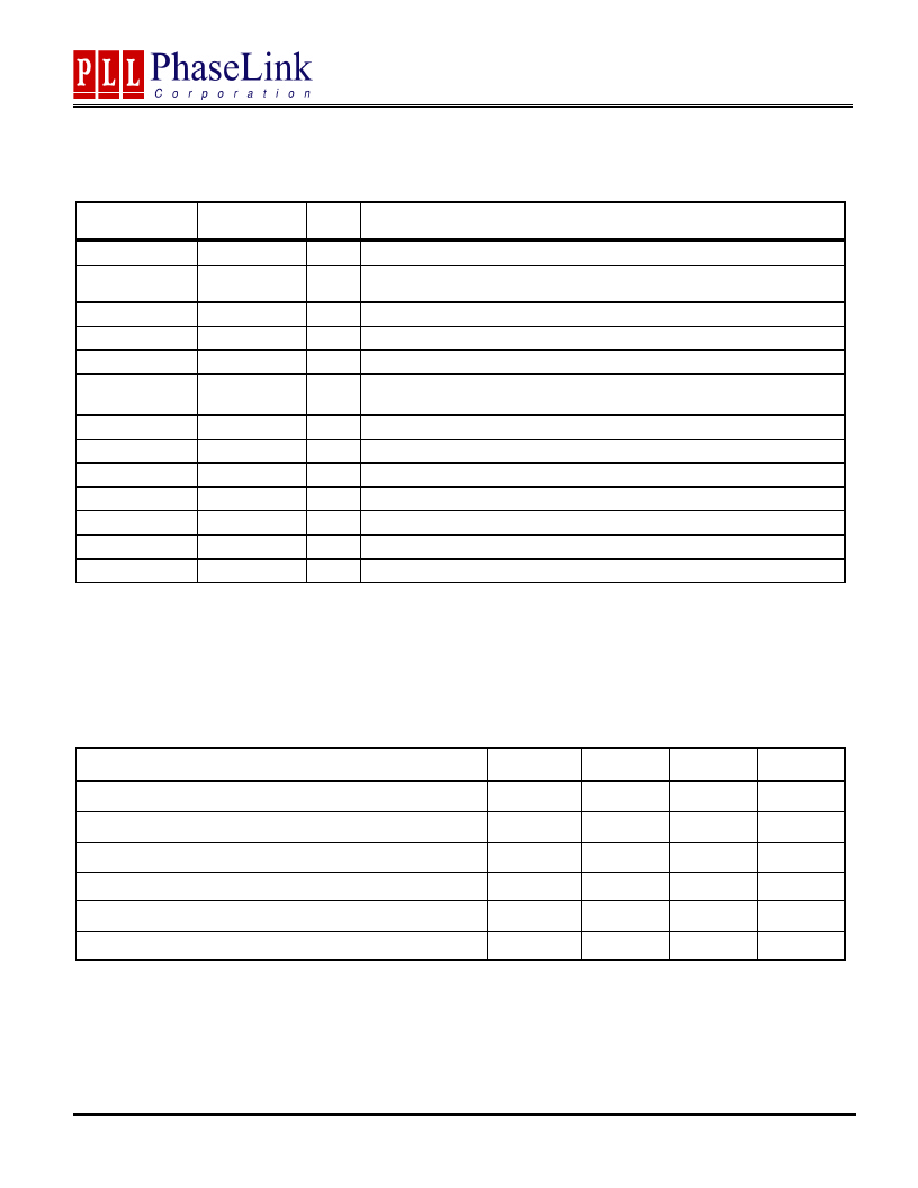
ELECTRICAL SPECIFICATIONS
1. Absolute Maximum Ratings
PARAMETERS
SYMBOL
MIN.
MAX.
UNITS
Supply Voltage Range
V
CC
-
0.5
7
V
Input Voltage Range
V
I
-
0.5
V
CC
+
0.5
V
Output Voltage Range
V
O
-
0.5
V
CC
+
0.5
V
Soldering Temperature
260
°
C
Storage Temperature
T
S
-65
150
°
C
Ambient Operating Temperature
0
70
°
C
Exposure of the device under conditions beyond the limits specified by Maximum Ratings for extended periods may cause permanent damage to the
device and affect product reliability. These conditions represent a stress rating only, and functional operations of the device at these or any other con-
ditions above the operational limits noted in this specification is not implied.

Preliminary for proposal
PLL130-01
High Speed Buffer for LVDS and PECL
47745 Fremont Blvd., Fremont, California 94538 TEL (510) 492-0990 FAX (510) 492-0991 Rev 07/13/01 Page 3
2. AC Specification
PARAMETERS
CONDITIONS
MIN.
TYP.
MAX. UNITS
Input Frequency
0
1300
MHz
Input signal swing
REF_IN input
100
mV
Output Frequency
0
1300
MHz
Output Rise Time
0.8V to 2.0V with no load
1.5
ns
Output Fall Time
2.0V to 0.8V with no load
1.5
ns
3. DC Specification
PARAMETERS
SYMBOL
CONDITIONS
MIN.
TYP.
MAX.
UNITS
Operating Voltage
VDD
3.135
3.465
V
Input High Voltage
V
IH
2
V
Input Low Voltage
V
IL
0.8
V
Input High Voltage
V
IH
TBD
V
Input Low Voltage
V
IL
TBD
V
AC coupling
TBD
TBD
100
mV
Output High Voltage
V
OH
I
OH
= TBD
TBD
V
Output Low Voltage
V
OL
I
OL
= TBD
TBD
V
Output High Voltage At
CMOS Level
V
OH
I
OH
= TBD
TBD
V
Operating Supply Current
I
DD
No Load
TBD
mA
Short-circuit Current
I
S
TBD
mA
Input Capacitance
C
IN
OE, Select Pins
5
pF

Preliminary for proposal
PLL130-01
High Speed Buffer for LVDS and PECL
47745 Fremont Blvd., Fremont, California 94538 TEL (510) 492-0990 FAX (510) 492-0991 Rev 07/13/01 Page 4
PACKAGE INFORMATION
ORDERING INFORMATION
PhaseLink Corporation, reserves the right to make changes in its products or specifications, or both at any time without notice. The information fur-
nished by Phaselink is believed to be accurate and reliable. However, PhaseLink makes no guarantee or warranty concerning the accuracy of said
information and shall not be responsible for any loss or damage of whatever nature resulting from the use of, or reliance upon this product.
LIFE SUPPORT POLICY: PhaseLink's products are not authorized for use as critical components in life support devices or systems without the ex-
press written approval of the President of PhaseLink Corporation.
For part ordering, please contact our Sales Department:
47745 Fremont Blvd., Fremont, CA 94538, USA
Tel: (510) 492-0990 Fax: (510) 492-0991
PART NUMBER
The order number for this device is a combination of the following:
Device number, Package type and Operating temperature range
PLL130-01 S C XX
PART NUMBER
TEMPERATURATURE
C=COMMERCIAL
M=MILITARY
I=INDUSTRAL
PACKAGE TYPE
S=SOIC, O=TSSOP, D=DIE
REVISION CODE
(when applicable)
C
L
A
16 PIN Narrow SOIC, TSSOP ( mm )
SOIC
TSSOP
Symbol
Min.
Max.
Min.
Max.
A
1.35
1.75
-
1.20
A1
0.10
0.25
0.05
0.15
B
0.33
0.51
0.19
0.30
C
0.19
0.25
0.09
0.20
D
9.80
10.00
4.90
5.10
E
3.80
4.00
4.30
4.50
H
5.80
6.20
6.40 BSC
L
0.40
1.27
0.45
0.75
e
1.27 BSC
0.65 BSC
E
H
D
A1
e
B