Document Outline
- FEATURES
- DESCRIPTION
- LIMITING VALUES
- ELECTRICAL CHARACTERISTICS
- THERMAL CHARACTERISTICS
- GRAPHICAL DATA
- PACKAGE OUTLINE
- DEFINITIONS
- LIFE SUPPORT APPLICATIONS
DATA SHEET
Product specification
2000 Feb 14
DISCRETE SEMICONDUCTORS
US1 series
SMA ultra fast low-loss
controlled avalanche rectifiers
book, halfpage
M3D168
2000 Feb 14
2
Philips Semiconductors
Product specification
SMA ultra fast low-loss
controlled avalanche rectifiers
US1 series
FEATURES
·
Glass passivated
·
High maximum operating temperature
·
Ideal for surface mount automotive applications
·
Low leakage current
·
Excellent stability
·
Guaranteed avalanche energy absorption capability
·
UL 94V-O classified plastic package
·
Shipped in 12 mm embossed tape
·
Marking: cathode, date code, type code
·
Easy pick and place.
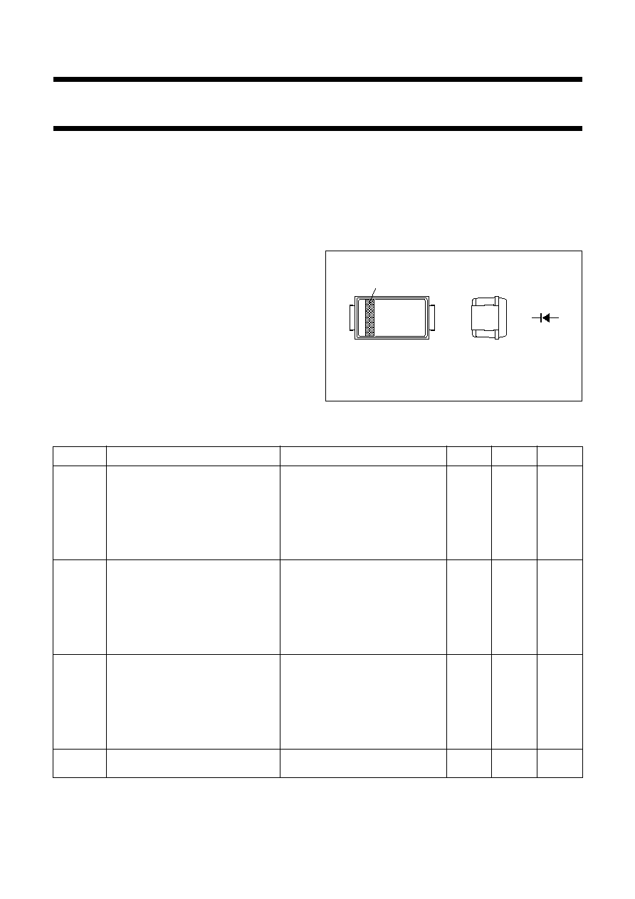
DESCRIPTION
DO-214AC surface mountable package with glass
passivated chip.
The well-defined void-free case is of a transfer-moulded
thermo-setting plastic. The small rectangular package has
two J bent leads.
olumns
MSA474
Top view
Side view
cathode
band
k
a
Fig.1 Simplified outline (DO-214AC) and symbol.
LIMITING VALUES
In accordance with the Absolute Maximum Rating System (IEC 134).
SYMBOL
PARAMETER
CONDITIONS
MIN.
MAX.
UNIT
V
RRM
repetitive peak reverse voltage
US1A
-
50
V
US1B
-
100
V
US1D
-
200
V
US1G
-
400
V
US1J
-
600
V
V
R
continuous reverse voltage
US1A
-
50
V
US1B
-
100
V
US1D
-
200
V
US1G
-
400
V
US1J
-
600
V
V
RMS
root mean square voltage
US1A
-
35
V
US1B
-
70
V
US1D
-
140
V
US1G
-
280
V
US1J
-
420
V
I
F(AV)
average forward current
averaged over any 20 ms period;
T
tp
= 110
°
C; see Fig.2
-
1
A

2000 Feb 14
3
Philips Semiconductors
Product specification
SMA ultra fast low-loss
controlled avalanche rectifiers
US1 series
ELECTRICAL CHARACTERISTICS
T
j
= 25
°
C unless otherwise specified.
THERMAL CHARACTERISTICS
Notes
1. Device mounted on Al
2
O
3
printed-circuit board, 0.7 mm thick; thickness of copper
35
µ
m.
2. Device mounted on epoxy-glass printed-circuit board, 1.5 mm thick; thickness of copper
40
µ
m. For more
information please refer to the
`General Part of associated Handbook'.
I
FSM
non-repetitive peak forward current
t = 8.3 ms half sine wave;
T
j
= 25
°
C prior to surge;
V
R
= V
RRMmax
-
25
A
T
stg
storage temperature
-
65
+175
°
C
T
j
junction temperature
See Fig.3
-
65
+175
°
C
SYMBOL
PARAMETER
CONDITIONS
TYP.
MAX.
UNIT
V
F
forward voltage
I
F
= 1 A;
US1A to US1G
see Fig.4
-
1.1
V
US1J
see Fig.5
-
1.4
V
I
R
reverse current
V
R
= V
RRMmax
; see Figs 6 and 7
-
10
µ
A
V
R
= V
RRMmax
; T
j
= 165
°
C; see Figs 6 and 7
-
50
µ
A
t
rr
reverse recovery time
when switched from I
F
= 0.5 A to I
R
= 1 A;
measured at I
R
= 0.25 A; see Fig.12
-
50
ns
C
d
diode capacitance
V
R
= 4 V; f = 1 MHz;
US1A to US1G
see Fig.8
14
-
pF
US1J
see Fig.9
10
-
pF
SYMBOL
PARAMETER
CONDITIONS
VALUE
UNIT
R
th j-tp
thermal resistance from junction to tie-point; see Fig.10
27
K/W
R
th j-a
thermal resistance from junction to ambient
note 1
100
K/W
note 2
150
K/W
SYMBOL
PARAMETER
CONDITIONS
MIN.
MAX.
UNIT

2000 Feb 14
4
Philips Semiconductors
Product specification
SMA ultra fast low-loss
controlled avalanche rectifiers
US1 series
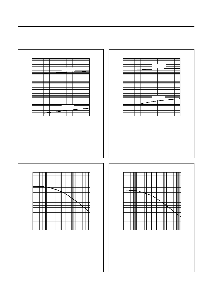
GRAPHICAL DATA
handbook, halfpage
0
40
200
2
1.5
0.5
0
1
80
Ttp (
°
C)
IF(AV)
(A)
120
160
MCD822
Fig.2
Maximum permissible average forward
current as a function of tie-point
temperature (including losses due to
reverse leakage).
V
R
= V
RRMmax
;
= 0.5; a = 1.57.
handbook, halfpage
0
100
VR (%VRmax)
Tj
(
°
C)
200
0
100
50
MBK455
Device mounted as shown in Fig.11.
Solid line: Al
2
O
3
printed-circuit board.
Dotted line: epoxy printed-circuit board.
Fig.3
Maximum permissible junction temperature
as a function of reverse voltage.
handbook, halfpage
3
2
VF (V)
IF
(A)
1
0
MCD792
10
2
10
1
10
-
1
10
-
2
10
-
3
US1A to G
T
j
= 25
°
C.
Fig.4
Forward current as a function of forward
voltage; typical values.
handbook, halfpage
4
2
IF
(A)
VF (V)
1
0
3
MCD793
10
2
10
1
10
-
1
10
-
2
10
-
3
US1J
T
j
= 25
°
C.
Fig.5
Forward current as a function of forward
voltage; typical values.
2000 Feb 14
5
Philips Semiconductors
Product specification
SMA ultra fast low-loss
controlled avalanche rectifiers
US1 series
handbook, halfpage
100
0
20
40
VR (%VRmax)
IR
(
µ
A)
60
80
10
2
10
1
10
-
1
10
-
2
10
-
3
MCD807
Tj = 165
°
C
Tj = 25
°
C
Fig.6
Reverse current as a function of reverse
voltage; typical values.
US1A to G
f = 1 MHz; T
j
= 25
°
C.
handbook, halfpage
100
0
20
40
VR (%VRmax)
IR
(
µ
A)
60
80
10
2
10
1
10
-
1
10
-
2
10
-
3
MCD806
Tj = 165
°
C
Tj = 25
°
C
Fig.7
Reverse current as a function of reverse
voltage; typical values.
US1J
f = 1 MHz; T
j
= 25
°
C.
handbook, halfpage
10
2
10
1
MCD798
10
-
2
10
-
1
1
VR (V)
Cd
(pF)
10
10
2
Fig.8
Diode capacitance as a function of reverse
voltage; typical values.
US1 A to G
f = 1 MHz; T
j
= 25
°
C.
handbook, halfpage
10
2
10
1
MCD797
10
-
2
10
-
1
1
VR (V)
Cd
(pF)
10
10
2
US1J
f = 1 MHz; T
j
= 25
°
C.
Fig.9
Diode capacitance as a function of reverse
voltage; typical values.