
1.
General description
The TEF6730 is a car radio tuner front-end for digital-IF reception, especially designed for
co-operation with digital-IF DSP back-ends of the SAF773x and SAF778x families.
The FM tuner features single conversion to IF = 10.7 MHz and integrated image rejection;
capable for FM 65 MHz to 108 MHz and weather band reception. The AM tuner features
single conversion to IF = 10.7 MHz with an integrated AM front-end, capable for LW, MW
and full SW reception. A combined AM/FM IF AGC amplifier provides a suitable IF signal
to the ADC in IF DSP.
The device can be controlled via the fast-mode I
2
C-bus (400 kHz) and includes
autonomous tuning functions for easy control. No manual alignments are required.
2.
Features
I
FM mixer for conversion of FM RF to IF 10.7 MHz with large dynamic range, high
image rejection and selectable mixer gain
I
Selectable high or low injection of LO
I
AGC PIN diode drive circuit for FM RF AGC with detection at RF and IF, including
keyed AGC function
I
RF input for weather band applications
I
Integrated AM front-end LNA
I
Integrated AM RF AGC for low desensitization and AGC PIN diode drive circuit with
detection at RF and IF
I
AM mixer for conversion of AM RF to IF 10.7 MHz
I
AM/FM IF AGC amplifier with large dynamic range, gain controlled from IF DSP
I
AM and FM front-end AGC information is available via the I
2
C-bus
I
Low phase noise local oscillator with reliable start-up behavior
I
In-lock detection for optimized adaptive PLL tuning speed
I
Programmable divider and mixer dividers for reception of FM (65 MHz to 108 MHz),
weather band, AM LW, MW and full SW
I
Two antenna DAAs
I
Sequential state machine supporting all tuning actions including AFU for RDS
I
Interfacing signals for IF AGC, FM keyed AGC, AFU and reference frequency to
IF DSP for optimum system performance
I
Software controlled flag outputs
I
Selection of four I
2
C-bus addresses
TEF6730
Front-end for digital-IF car radio
Rev. 01 -- 10 July 2006
Product data sheet

TEF6730_1
� Koninklijke Philips Electronics N.V. 2006. All rights reserved.
Product data sheet
Rev. 01 -- 10 July 2006
2 of 56
Philips Semiconductors
TEF6730
Front-end for digital-IF car radio
3.
Quick reference data
Table 1.
Quick reference data
V
CCA
= 8.5 V; T
amb
= 25
�
C; see
Figure 25
; all AC values are given in RMS; unless otherwise specified.
Symbol
Parameter
Conditions
Min
Typ
Max
Unit
Supply voltage
V
CCA
analog supply voltage
on pins V
CC
, V
CC(PLL)
, V
CC(VCO)
, V
CC(RF)
,
V
CC(IF)
, FMMIXOUT1, FMMIXOUT2,
AMMIXOUT1 and AMMIXOUT2
8
8.5
9
V
Current in FM mode
I
CC(tot)
total supply current
-
85.3
-
mA
Current in AM mode
I
CC(tot)
total supply current
-
114.7
-
mA
Antenna Digital Auto Alignment (DAA)
DAA1: pin DAAOUT1
[1]
G
conv(DAA)
DAA conversion gain
0.1
-
2
DAA2: pin DAAOUT2
[2]
G
conv(DAA)
DAA conversion gain
0.7
-
1.35
Reference frequency
External reference frequency, circuit inputs: pins FREF1 and FREF2
f
ext
external frequency
-
100
-
kHz
Tuning system; see
Table 28
,
Table 29
,
Table 30
and
Table 31
Voltage controlled oscillator
f
VCO(min)
minimum VCO frequency
[3]
-
-
130
MHz
application according to
Figure 25
[3]
-
-
159.9
MHz
f
VCO(max)
maximum VCO frequency
[3]
256
-
-
MHz
C/N
carrier-to-noise ratio
f
VCO
= 200 MHz;
f = 10 kHz; Q = 30
94
98
-
dBc/
Hz
Timings
t
tune
tuning time
Europe FM/US FM band; f
ref
= 100 kHz;
f
RF
= 87.5 MHz to 108 MHz
-
0.75
1
ms
AM MW band; f
ref
= 20 kHz;
f
RF
= 0.53 MHz to 1.7 MHz
-
-
10
ms
t
upd(AF)
AF update time
cycle time for inaudible AF update
including 1 ms mute start and 1 ms mute
release time
-
6
6.5
ms
AM overall system parameters
[4]
f
i(RF)
RF input frequency
LW
144
-
288
kHz
MW
522
-
1710
kHz
SW
2.3
-
26.1
MHz
f
IF
IF frequency
-
10.7
-
MHz
V
sens
sensitivity voltage
(S+N)/N = 26 dB
-
50
-
�
V

TEF6730_1
� Koninklijke Philips Electronics N.V. 2006. All rights reserved.
Product data sheet
Rev. 01 -- 10 July 2006
3 of 56
Philips Semiconductors
TEF6730
Front-end for digital-IF car radio
[1]
Conversion gain formula of DAA1:
where n = 0 to 127.
V
i(RF)
RF input voltage
start level of wideband AGC
data byte AGC bits WBAGC[1:0] = 00
-
125
-
mV
data byte AGC bits WBAGC[1:0] = 01
-
100
-
mV
data byte AGC bits WBAGC[1:0] = 10
-
75
-
mV
data byte AGC bits WBAGC[1:0] = 11
-
35
-
mV
V
i(RF)M
peak RF input voltage
start level of narrow-band AGC; m = 0
data byte AGC bits NBAGC[1:0] = 00
-
200
-
mV
data byte AGC bits NBAGC[1:0] = 01
-
170
-
mV
data byte AGC bits NBAGC[1:0] = 10
-
140
-
mV
data byte AGC bits NBAGC[1:0] = 11
-
115
-
mV
IP2
second-order intercept point referenced to receiver input
-
152
-
dB
�
V
IP3
third-order intercept point
referenced to receiver input
f = 40 kHz
-
130
-
dB
�
V
f = 100 kHz
-
133
-
dB
�
V
ripple
ripple rejection
V
CC(ripple)
/V
audio
; f
ripple
= 100 Hz;
V
CC(ripple)
= 10 mV (RMS);
V
i(RF)
= 1 mV to 1 V
-
40
-
dB
FM overall system parameters
[5]
f
i(RF)
RF input frequency
FM standard
65
-
108
MHz
weather band
162.4
-
162.55 MHz
f
IF
IF frequency
-
10.7
-
MHz
V
sens
sensitivity voltage
B
IF
= 170 kHz
-
2
-
�
V
threshold extension enabled; weak signal
handling enabled (SAF7730 N231)
-
1.1
-
�
V
V
i(RF)
RF input voltage
start level of wideband AGC
data byte AGC bits WBAGC[1:0] = 00
-
19
-
mV
data byte AGC bits WBAGC[1:0] = 01
-
14
-
mV
data byte AGC bits WBAGC[1:0] = 10
-
10
-
mV
data byte AGC bits WBAGC[1:0] = 11
-
7
-
mV
V
i(RF)M
peak RF input voltage
start level of narrow-band AGC; m = 0
data byte AGC bits NBAGC[1:0] = 00
-
17
-
mV
data byte AGC bits NBAGC[1:0] = 01
-
14
-
mV
data byte AGC bits NBAGC[1:0] = 10
-
11
-
mV
data byte AGC bits NBAGC[1:0] = 11
-
9
-
mV
IP3
third-order intercept point
f = 400 kHz
-
123
-
dB
�
V
ripple
ripple rejection
V
CC(ripple)
/V
audio
; f
ripple
= 100 Hz;
V
CC(ripple)
= 10 mV (RMS);
V
i(RF)
= 500
�
V
-
64
-
dB
Table 1.
Quick reference data
...continued
V
CCA
= 8.5 V; T
amb
= 25
�
C; see
Figure 25
; all AC values are given in RMS; unless otherwise specified.
Symbol
Parameter
Conditions
Min
Typ
Max
Unit
V
DAAOUT 1
1.915
n
128
---------
�
0.1
+
V
tune
�
=

TEF6730_1
� Koninklijke Philips Electronics N.V. 2006. All rights reserved.
Product data sheet
Rev. 01 -- 10 July 2006
4 of 56
Philips Semiconductors
TEF6730
Front-end for digital-IF car radio
[2]
Conversion gain formula of DAA2:
where n = 0 to 15.
[3]
The VCO frequency is determined by the external circuit at pins OSCFDB and OSCTNK.
[4]
Based on 15 pF/60 pF dummy aerial, voltages at dummy aerial input, f
mod
= 400 Hz, 2.5 kHz audio bandwidth, f
i(RF)
= 990 kHz, m = 0.3
and nominal maximum IF AGC gain, unless otherwise specified.
[5]
Based on 75
dummy aerial, voltages at dummy aerial input, f
mod
= 400 Hz, de-emphasis = 50
�
s, f
i(RF)
= 97.1 MHz,
f = 22.5 kHz,
nominal mixer gain and nominal maximum IF AGC gain, unless otherwise specified.
4.
Ordering information
V
DAAOUT 2
0.693
n
16
------
�
0.7
+
V
DAAOUT 1
�
=
Table 2.
Ordering information
Type number Package
Name
Description
Version
TEF6730HW
HTQFP64
plastic thermal enhanced thin quad flat package; 64 leads; body 10 x 10 x 1 mm;
exposed die pad
SOT855-1

xxxx xxxxxxxxxxxxxxxxxxxxxxxxxxxxxx x xxxxxxxxxxxxxx xxxxxxxxxx xxx xxxxxx xxxxxxxxxxxxxxxxxxxxxxx xxxxxxxxxxxxxxxxxxxxxx
xxxxx xxxxxx xx xxxxxxxxxxxxxxxxxxxxxxxxxxxxx xxxxxxxxxxxxxxxxxxxxxx xxxxxxxxxxx xxxxxxx xxxxxxxxxxxxxxxxxxx
xxxxxxxxxxxxxxxx xxxxxxxxxxxxxx xxxxxx xx xxxxxxxxxxxxxxxxxxxxxxxxxxxxxxxx xxxxxxxxxxxxxxxxxxxxxxxx xxxxxxx
xxxxxxxxxxxxxxxxxxxxxxxxxxxxxxxxxxxxxxxxxxxxxx xxxxxxxxxxx xxxxx x x
TEF6730_1
� K
oninklijk
e Philips Electronics N.V
. 2006. All r
ights reser
v
ed.
Pr
oduct data sheet
Re
v
.
01 -- 10 J
u
l
y
2006
5 of 56
Philips Semiconductor
s
TEF6730
Fr
ont-end f
or digital-IF car radio
5.
Bloc
k dia
gram
Fig 1.
Block diagram of TEF6730HW
ifagc
FM
ifagc
ifagc
lna rf
lna
rf
62
63
64
1
2
3
4
5
7
8
10 9
11
12
13
14
15
17
19
20
21
22
23
24
25
31
34
30
26
27
28
29
32
33
35
36
39
40
IFMAGC
FMMIXIN1
FMMIXIN2
WXMIXIN
WXMIXDEC
DAAOUT1
DAAOUT2
VTUNE
CPOUT
OSCFDB
OSCTNK
37
38
41
53
54
55
56
57
45
52
16, 18, 48, 49
V
CC(PLL)
VCOGND
V
CC(VCO)
FREF1
FREF2
VREF
GND
V
CC
FGND
DGND
i.c.
43
42
44
46
47
50
51
58
59
60
61
6
FMMIXOUT2
AMMIXOUT2
FMMIXOUT1
CFSW2
CFSW1
SWDEC
IFAGCDEC
FMIFAGCIN2
FMIFAGCIN1
AMIFAGCIN
IFAGCBIAS
IFGND
V
CC(IF)
AMMIXOUT1
V
CC(RF)
V50LNA
LNAIN
AGCCNTRL
LNAOUT
LNAAGCDEC
AMMIXDEC
AMMIXIN
TAMAGC
PINAGCDEC
IAMAGC
RFGND
TFMAGC
KAGC
antenna DAA
TEF6730HW
AM RF
AGC
FM RF
AGC
BAND
�
M
REF
f
ref
MIXER
MIXER
MIXER
PLL
�
N
IF AGC
AM LNA
TUNING
STATE
MACHINE
I
2
C-BUS
tuner
control
CTRL
BUF
read
address
pll in-lock
write
IFOUT1
am/fm
rf agc
IFOUT2
IFAGCMSB
IFAGCLSB
001aae088
ADDR2
ADDR1
SDA
SWPORT
AFSAMPLE
AFHOLD
SCL
vco
vco
vref
sup
sup
fgnd
dig
i.c.
flag
pll
90
�
WX
90
�

TEF6730_1
� Koninklijke Philips Electronics N.V. 2006. All rights reserved.
Product data sheet
Rev. 01 -- 10 July 2006
6 of 56
Philips Semiconductors
TEF6730
Front-end for digital-IF car radio
6.
Pinning information
6.1 Pinning
6.2 Pin description
Fig 2.
Pin configuration for HTQFP64
TEF6730HW
AMIFAGCIN
i.c.
FMIFAGCIN1
ADDR1
FMIFAGCIN2
ADDR2
IFAGCDEC
FGND
SWDEC
AFHOLD
CFSW1
AFSAMPLE
CFSW2
SWPORT
FMMIXOUT1
V
CC(VCO)
AMMIXOUT2
OSCTNK
FMMIXOUT2
OSCFDB
AMMIXOUT1
VCOGND
V
CC(RF)
V
CC(PLL)
V50LNA
CPOUT
LNAIN
VTUNE
AGCCNTRL
KAGC
i.c.
DAAOUT2
LNAOUT
IFAGCBIAS
i.c.
IFGND
LNAAGCDEC
V
CC(IF)
AMMIXDEC
IFAGCLSB
AMMIXIN
IFAGCMSB
TAMAGC
IFOUT2
PINAGCDEC
IFOUT1
IAMAGC
V
CC
RFGND
GND
FMMIXIN1
VREF
FMMIXIN2
FREF2
WXMIXIN
FREF1
WXMIXDEC
DGND
IFMAGC
SCL
TFMAGC
SDA
DAAOUT1
i.c.
001aae089
1
2
3
4
5
6
7
8
9
10
11
12
13
14
15
16
48
47
46
45
44
43
42
41
40
39
38
37
36
35
34
33
17
18
19
20
21
22
23
24
25
26
27
28
29
30
31
32
64
63
62
61
60
59
58
57
56
55
54
53
52
51
50
49
Table 3.
Pin description
Symbol
Pin
Description
AMIFAGCIN
1
IF AGC amplifier AM input (10.7 MHz)
FMIFAGCIN1
2
IF AGC amplifier FM input 1 (10.7 MHz)
FMIFAGCIN2
3
IF AGC amplifier FM input 2 (10.7 MHz)
IFAGCDEC
4
IF AGC amplifier AM and FM decoupling
SWDEC
5
ceramic filter switch decoupling
CFSW1
6
ceramic filter switch 1
CFSW2
7
ceramic filter switch 2
FMMIXOUT1
8
FM mixer IF output 1 (10.7 MHz)
AMMIXOUT2
9
AM mixer IF output 2 (10.7 MHz)

TEF6730_1
� Koninklijke Philips Electronics N.V. 2006. All rights reserved.
Product data sheet
Rev. 01 -- 10 July 2006
7 of 56
Philips Semiconductors
TEF6730
Front-end for digital-IF car radio
FMMIXOUT2
10
FM mixer IF output 2 (10.7 MHz)
AMMIXOUT1
11
AM mixer IF output 1 (10.7 MHz)
V
CC(RF)
12
AM/FM RF supply voltage
V50LNA
13
AM LNA supply voltage decoupling
LNAIN
14
AM LNA input
AGCCNTRL
15
AM LNA AGC pin
i.c.
16
internally connected; leave open
LNAOUT
17
AM LNA output
i.c.
18
internally connected; leave open
LNAAGCDEC
19
AM LNA AGC decoupling
AMMIXDEC
20
AM mixer decoupling
AMMIXIN
21
AM mixer input
TAMAGC
22
AM RF AGC time constant
PINAGCDEC
23
AM PIN diode AGC decoupling
IAMAGC
24
AGC current for AM PIN diode
RFGND
25
RF ground
FMMIXIN1
26
FM mixer input 1
FMMIXIN2
27
FM mixer input 2
WXMIXIN
28
weather band mixer input
WXMIXDEC
29
weather band mixer decoupling
IFMAGC
30
AGC current for FM PIN diode
TFMAGC
31
FM RF AGC time constant
DAAOUT1
32
antenna DAA output 1
DAAOUT2
33
antenna DAA output 2
KAGC
34
level input for FM keyed AGC function
VTUNE
35
tuning voltage input antenna DAA
CPOUT
36
charge pump output
V
CC(PLL)
37
tuning PLL supply voltage
VCOGND
38
VCO ground
OSCFDB
39
VCO feedback
OSCTNK
40
VCO tank circuit
V
CC(VCO)
41
VCO supply voltage
SWPORT
42
software controllable port output
AFSAMPLE
43
AF sample flag output
AFHOLD
44
AF hold flag output and input
FGND
45
reference frequency ground
ADDR2
46
address select input 2
ADDR1
47
address select input 1
i.c.
48
internally connected; leave open
i.c.
49
internally connected; leave open
SDA
50
I
2
C-bus data line input and output
Table 3.
Pin description
...continued
Symbol
Pin
Description

TEF6730_1
� Koninklijke Philips Electronics N.V. 2006. All rights reserved.
Product data sheet
Rev. 01 -- 10 July 2006
8 of 56
Philips Semiconductors
TEF6730
Front-end for digital-IF car radio
7.
Functional description
7.1 FM mixer 1
The FM quadrature mixer converts FM RF (65 MHz to 108 MHz) to an IF frequency of
10.7 MHz. The FM mixer provides high image rejection, a large dynamic range and
selectable mixer gain. The image rejection can be selected between low injection of LO
and high injection of LO via the I
2
C-bus independently of the band selection. A separate
RF input for weather band is available.
7.2 FM RF AGC
AGC detection at the FM front-end mixer input and the AM/FM IF AGC amplifier input,
both with programmable AGC thresholds. When the threshold is exceeded, the PIN diode
drive circuit sources a current to an external PIN diode circuit, keeping the RF signal level
constant.
Keyed AGC function is selectable via the I
2
C-bus and uses the in-band level information
from the IF DSP.
The AGC PIN diode drive circuit can optionally deliver a fixed current as a local function.
In AM mode, the AGC PIN diode drive circuit can be set to generate a fixed source current
into the external FM PIN diode circuitry.
7.3 Antenna DAA1 and DAA2
The antenna DAA1 measures the VCO tuning voltage and multiplies it with a factor
defined by the 7-bit DAA1 setting to generate a tuning voltage for the FM antenna tank
circuit. If a second FM tank circuit is applied, the tuning voltage can be derived from the
antenna DAA2 output. The antenna DAA2 measures the output voltage of the antenna
DAA1 and multiplies it with a factor defined by the 4-bit DAA2 setting.
SCL
51
I
2
C-bus clock line input
DGND
52
digital ground
FREF1
53
reference frequency input 1
FREF2
54
reference frequency input 2
VREF
55
reference voltage noise decoupling
GND
56
ground
V
CC
57
supply voltage (8.5 V)
IFOUT1
58
IF AGC amplifier output 1
IFOUT2
59
IF AGC amplifier output 2
IFAGCMSB
60
MSB input for IF AGC amplifier gain setting
IFAGCLSB
61
LSB input for IF AGC amplifier gain setting
V
CC(IF)
62
IF AGC amplifier supply voltage
IFGND
63
IF AGC amplifier ground
IFAGCBIAS
64
bias voltage decoupling for IF AGC amplifier
Table 3.
Pin description
...continued
Symbol
Pin
Description

TEF6730_1
� Koninklijke Philips Electronics N.V. 2006. All rights reserved.
Product data sheet
Rev. 01 -- 10 July 2006
9 of 56
Philips Semiconductors
TEF6730
Front-end for digital-IF car radio
7.4 AM LNA
The AM low noise amplifier is fully integrated.
7.5 AM RF AGC
The AM RF AGC is partially integrated. Detection is at the output of the AM LNA and at
the input of the AM/FM IF AGC amplifier, both with programmable thresholds. First the
integrated AGC reduces the gain of the LNA. After the LNA AGC, the PIN diode AGC
takes over by sinking a current via an external PIN diode.
In FM mode, the AM AGC can be set to a fixed attenuation.
7.6 AM mixer
The large dynamic range AM mixer converts AM RF (144 kHz to 26.1 MHz) to an IF
frequency of 10.7 MHz.
7.7 VCO and dividers
The varactor tuned LC oscillator together with the dividers provides the LO signal for both
AM and FM front-end mixers. The VCO has an operating frequency of approximately
160 MHz to 256 MHz. In FM mode the LO frequency is divided by 2 or 3. These dividers
generate in-phase and quadrature-phase output signals used in the FM front-end mixer
for image rejection. In weather band mode the LO signal is directly phase shifted to
generate the in-phase and quadrature-phase signals. In AM mode the LO frequency is
divided by 6, 8, 10, 16 or 20 depending on the selected AM band.
7.8 Tuning PLL
The tuning PLL locks the VCO frequency divided by the programmable divider ratio to the
reference frequency. Due to the combination of different charge pump signals in the
PLL loop filter, the loop parameters are adapted dynamically. Tuning to different
RF frequencies is done by changing the programmable divider ratio. The tuning step size
is selected with the reference frequency divider setting.
7.9 AM/FM IF AGC amplifier
The combined AM/FM IF AGC amplifier delivers a suitable IF signal for the ADC in the
IF DSP. The maximum gain of the IF AGC amplifier can be selected via the I
2
C-bus. The
gain of this amplifier is automatically adapted via interfacing signals from the IF DSP. The
IF AGC amplifier has three signal inputs, two for FM and one for AM. This allows the
application of multiple external filters, e.g. with different bandwidths.
8.
I
2
C-bus protocol
Fig 3.
Write mode
ACK-s
ACK-s
DATA
SLAVE ADDRESS W
data transferred
(n bytes
+
acknowledge)
001aad051
P
S
ACK-s
MSA

TEF6730_1
� Koninklijke Philips Electronics N.V. 2006. All rights reserved.
Product data sheet
Rev. 01 -- 10 July 2006
10 of 56
Philips Semiconductors
TEF6730
Front-end for digital-IF car radio
8.1 Read mode
Read data is loaded into the I
2
C-bus register at the preceding acknowledge clock pulse.
8.1.1 Read mode: data byte TUNER
Fig 4.
Read mode
DATA
ACK-s
ACK-m
DATA
NA
SLAVE ADDRESS R
001aad049
P
S
data transferred
(n
-
1 bytes
+
acknowledge)
Table 4.
Description of I
2
C-bus format
Code
Description
S
START condition
Slave address W
1100 0000b for pin ADDR2 and pin ADDR1 grounded
1100 0010b for pin ADDR2 grounded and pin ADDR1 floating
1100 0100b for pin ADDR2 floating and pin ADDR1 grounded
1100 0110b for pin ADDR2 and pin ADDR1 floating
Slave address R
1100 0001b for pin ADDR2 and pin ADDR1 grounded
1100 0011b for pin ADDR2 grounded and pin ADDR1 floating
1100 0101b for pin ADDR2 floating and pin ADDR1 grounded
1100 0111b for pin ADDR2 and pin ADDR1 floating
ACK-s
acknowledge generated by the slave
ACK-m
acknowledge generated by the master
NA
not acknowledge
MSA
mode and subaddress byte
Data
data byte
P
STOP condition
Table 5.
Read register overview
Data byte
Name
Reference
0h
TUNER
Section 8.1.1
1h
ID
Section 8.1.2
Table 6.
TUNER - data byte 0h bit allocation
7
6
5
4
3
2
1
0
RAGC1
RAGC0
TAS1
TAS0
-
-
-
POR

TEF6730_1
� Koninklijke Philips Electronics N.V. 2006. All rights reserved.
Product data sheet
Rev. 01 -- 10 July 2006
11 of 56
Philips Semiconductors
TEF6730
Front-end for digital-IF car radio
8.1.2 Read mode: data byte ID
8.2 Write mode
The tuner is controlled by the I
2
C-bus. After the IC address the MSA byte contains the
control of the tuning action via the bits MODE[2:0] and REGC and subaddressing via bits
SA[3:0] (see
Figure 5
).
Table 7.
TUNER - data byte 0h bit description
Bit
Symbol
Description
7 and 6
RAGC[1:0]
RF AGC attenuation indicator, PIN diode current on pin IFMAGC
AM mode:
00 = no AGC
01 = LNA AGC
10 = I
AGC
< 1 mA
11 = I
AGC
> 1 mA
FM mode:
00 = < 0.1 mA
01 = 0.1 mA to 0.5 mA
10 = 0.5 mA to 2.5 mA
11 = > 2.5 mA
5 and 4
TAS[1:0]
tuning action state; the signal TAS informs about internal control
functions of the tuner action state machine; this way the progress of
tuner actions can be monitored by the microcontroller;
see
Figure 8
to
Figure 18
00 = no current action
01 = mute started and in progress at DSP
10 = PLL tuning in progress and mute activated at DSP
11 = PLL tuning ready and mute activated at DSP
3 to 1
-
not used
0
POR
power-on reset
0 = normal operation
1 = I
2
C-bus data is reset to default POR state; POR is reset to
logic 0 after the TEF6730 has been read out and written to via
I
2
C-bus at least once
Table 8.
ID - data byte 1h bit allocation
7
6
5
4
3
2
1
0
-
-
-
-
-
ID2
ID1
ID0
Table 9.
ID - data byte 1h bit description
Bit
Symbol
Description
7 to 3
-
not used
2 to 0
ID[2:0]
device type identification 110 = TEF6730

TEF6730_1
� Koninklijke Philips Electronics N.V. 2006. All rights reserved.
Product data sheet
Rev. 01 -- 10 July 2006
12 of 56
Philips Semiconductors
TEF6730
Front-end for digital-IF car radio
The tuner circuit is controlled by the CONTROL register. Any data change in the
CONTROL register has immediate effect and will change the operation of the tuner circuit
accordingly. Transmitted I
2
C-bus data is not loaded into the CONTROL register directly
but loaded into a BUFFER register instead. This allows the IC to take care of tuning
actions freeing the microcontroller from cumbersome controls and timings.
Controlled by a state machine, the BUFFER data will be loaded into the CONTROL
register for new settings. However, at the same time the CONTROL data is loaded into the
BUFFER register. This register swap action allows a fast return to the previous setting
because the previous data remains available in the BUFFER register (see
Figure 6
and
Figure 7
).
Via MODE several operational modes can be selected for the state machine. MODE offers
all standard tuning actions as well as generic control for flexibility. The state machine
controls the tuner by controlling the internal I
2
C-bus data. Action progress is monitored by
the accompanying IF DSP via the AFSAMPLE and AFHOLD lines. This way, functions like
tuning mute and weak signal processing can be controlled complementary to the tuner
action.
The state machine operation starts at the end of transmission (P = STOP). In case a
previous action is still active, this is ignored and the new action defined by MODE is
started immediately. When only the address byte is transmitted, no action is started at all
(device presence test).
To minimize the I
2
C-bus transmission time, only bytes that include data changes need to
be written. Following the MSA byte the transmission can start at any given data byte
defined by the subaddress (SA) bits.
Furthermore, when writing the buffered range either the current BUFFER data or the
current CONTROL data can be used as default, controlled by the REGC bit:
�
With REGC = 0, any BUFFER data that is not newly written via I
2
C-bus remains
unchanged. In general, the BUFFER register will contain the previous tuner setting, so
this becomes default for the new setting. When only the MSA byte is transmitted
defining a tuning MODE with REGC = 0, the tuner will return to its previous settings
(see
Figure 6
).
�
With REGC = 1, the BUFFER register is loaded with data from the CONTROL register
first. This way, not written BUFFER data equals the CONTROL data. Since the
CONTROL register contains the current tuner setting with REGC = 1, the current
tuner setting is default for the new setting. When a tuning MODE action is defined with
REGC = 1, the tuner will keep its current settings (CONTROL = current) for all data
that is not newly written during the transmission (see
Figure 7
).
After power-on reset, all registers are in their default settings. The control signals for the
IF DSP are set to AFSAMPLE = HIGH and AFHOLD = HIGH (i.e. mute state). Any action
of the state machine will change this setting to a new one as defined by the bits
MODE[2:0].

TEF6730_1
� Koninklijke Philips Electronics N.V. 2006. All rights reserved.
Product data sheet
Rev. 01 -- 10 July 2006
13 of 56
Philips Semiconductors
TEF6730
Front-end for digital-IF car radio
Table 10.
Write mode subaddress overview
Subaddress
Name
Default
Reference
0h
CONTROL
0000 0100b
Section 8.2.2
1h
PLLM
0000 1000b
Section 8.2.3
2h
PLLL
0111 1110b
Section 8.2.4
3h
DAA
0100 0000b
Section 8.2.5
4h
AGC
1000 0000b
Section 8.2.6
5h
BAND
0010 0000b
Section 8.2.7
Fh
TEST
0000 0000b
Section 8.2.8
Fig 5.
I
2
C-bus control
001aae094
AFSAMPLE
SA = 00h to 05h
load
REGC = 1
swap
MODE
AFHOLD
CONTROL REGISTER
SA = 00h to 05h
BUFFER REGISTER
SA = 00h to 05h
MODE DECODER
TUNER CIRCUIT
I
2
C-BUS
STATE MACHINE

TEF6730_1
� Koninklijke Philips Electronics N.V. 2006. All rights reserved.
Product data sheet
Rev. 01 -- 10 July 2006
14 of 56
Philips Semiconductors
TEF6730
Front-end for digital-IF car radio
Fig 6.
Write to CONTROL register with swap, REGC = 0
001aae095
CONTROL
BUFFER
MODE = load, REGC = 0, SA = 2
swap
address
new
MSA
byte 2
byte 3
byte 4
byte 5
P
byte 0
previous
current
byte 1
previous
current
byte 0
current
previous
byte 1
current
previous
byte 2
current
new
byte 3
current
new
byte 4
current
new
byte 5
current
new
byte 2
previous
current
new
byte 3
previous
current
new
byte 4
previous
current
new
byte 5
previous
current

TEF6730_1
� Koninklijke Philips Electronics N.V. 2006. All rights reserved.
Product data sheet
Rev. 01 -- 10 July 2006
15 of 56
Philips Semiconductors
TEF6730
Front-end for digital-IF car radio
Fig 7.
Write to CONTROL register with swap, REGC = 1
001aae096
CONTROL
BUFFER
MODE = load, REGC = 1, SA = 3
load
address
MSA
byte 3
byte 4
byte 5
P
byte 0
previous
current
byte 1
previous
current
byte 2
previous
current
byte 0
current
current
byte 1
current
current
byte 2
current
current
byte 3
current
new
byte 4
current
new
byte 5
current
current
current
current
current
current
current
new
new
byte 3
previous
current
new
byte 4
previous
current
new
byte 5
previous
current
swap

TEF6730_1
� Koninklijke Philips Electronics N.V. 2006. All rights reserved.
Product data sheet
Rev. 01 -- 10 July 2006
16 of 56
Philips Semiconductors
TEF6730
Front-end for digital-IF car radio
8.2.1 Mode and subaddress byte for write
[1]
When the write transmission of a state machine command starts during a mute state of the state machine,
the sequences of the state machine start immediately with the actions which follow the mute period in the
standard sequence (see
Figure 9
,
Figure 11
,
Figure 13
,
Figure 15
and
Figure 17
).
[2]
References to mute are only used for better understanding. Muting is performed in the IF DSP controlled by
the tuner AFHOLD and AFSAMPLE lines.
[3]
In the modes preset and search the AM AGC time constant is set to fast during the period of complete
mute.
[4]
The AF update sequence can also be started by pulling the AFHOLD pin LOW. In this case the AF
information should be loaded into the BUFFER before. LOW period for a correct AF update timing:
t
LOW
> 20
�
s. Between the end of the I
2
C-bus transmission and the falling edge of the AFHOLD pulse a
delay of
20
�
s is necessary.
Table 11.
MSA - mode and subaddress byte bit allocation
7
6
5
4
3
2
1
0
MODE2
MODE1
MODE0
REGC
SA3
SA2
SA1
SA0
Table 12.
MSA - mode and subaddress byte bit description
Bit
Symbol
Description
7 to 5
MODE[2:0]
mode; see
Table 13
4
REGC
register mode
0 = buffer mode or back mode: previous tuning data is default for
new I
2
C-bus write (data of the BUFFER register is not changed
before I
2
C-bus write); see
Figure 6
1 = control mode or current mode: current tuning data is default for
new I
2
C-bus write (the BUFFER register is loaded with CONTROL
register data before I
2
C-bus write); see
Figure 7
3 to 0
SA[3:0]
subaddress; write data byte subaddress 0 to 15. The subaddress
value is auto-incremented and will revert from SA = 15 to SA = 0. The
auto-increment function cannot be switched off.
Table 13.
Tuning action modes
[1]
MODE2 MODE1 MODE0 Symbol
Description
[2]
0
0
0
buffer
write BUFFER register, no state machine action, no
swap
0
0
1
preset
tune to new program with 60 ms mute control; swap
[3]
;
see
Figure 8
and
Figure 9
0
1
0
search
tune to new program and stay muted (for release use
end mode); swap
[3]
; see
Figure 10
and
Figure 11
0
1
1
AF update
tune to AF program; check AF quality and tune back
to main program; two swap operations
[4]
;
see
Figure 12
and
Figure 13
1
0
0
jump
tune to AF program in minimum time; swap;
see
Figure 14
and
Figure 15
1
0
1
check
tune to AF program and stay muted (for release use
end mode); swap; see
Figure 16
and
Figure 17
1
1
0
load
write CONTROL register via BUFFER; no state
machine action; immediate swap; see
Figure 6
and
Figure 7
1
1
1
end
end action; release mute; no swap; see
Figure 18

TEF6730_1
� Koninklijke Philips Electronics N.V. 2006. All rights reserved.
Product data sheet
Rev. 01 -- 10 July 2006
17 of 56
Philips Semiconductors
TEF6730
Front-end for digital-IF car radio
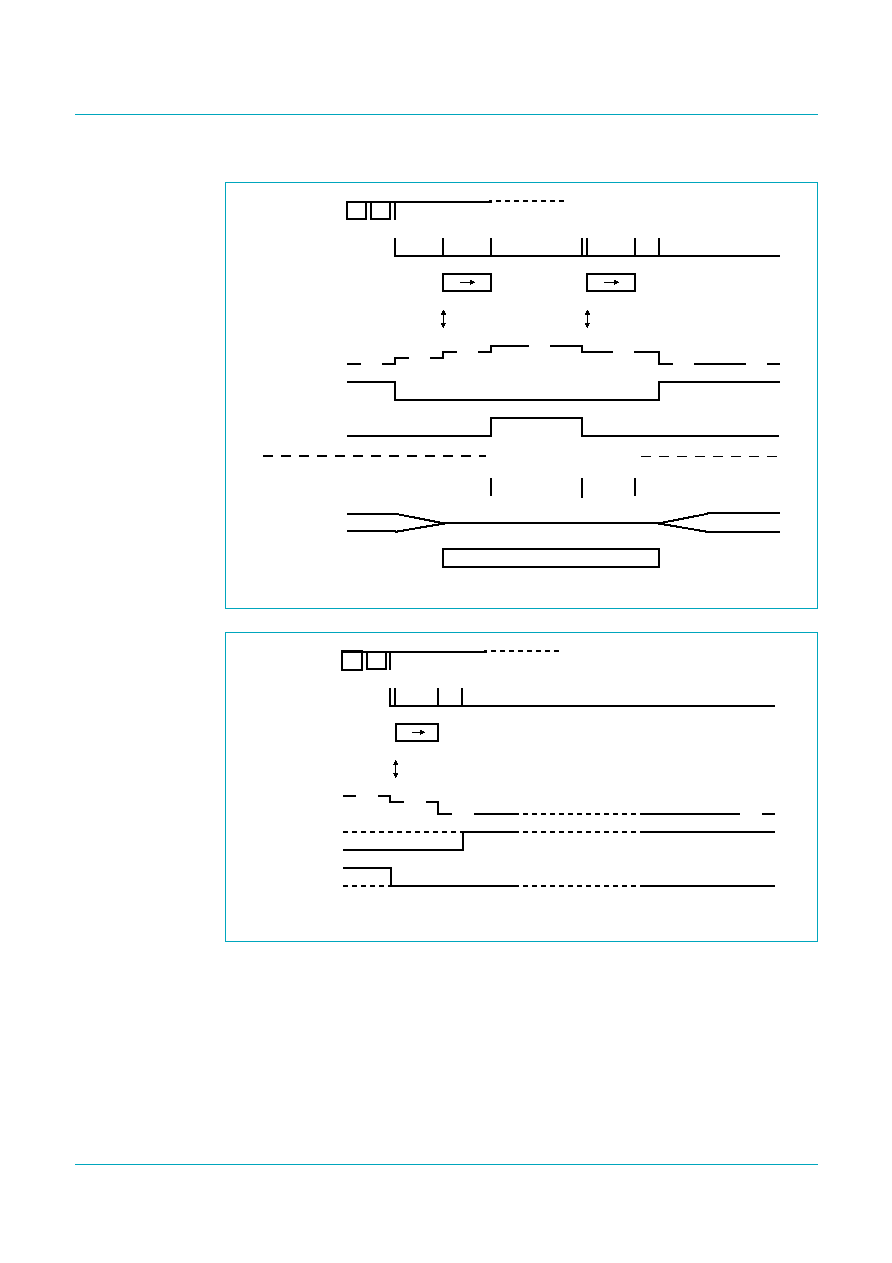
Fig 8.
Preset mode
Fig 9.
Preset mode, started during mute
001aae097
1 ms
PLL
FAST
50
�
s
suggested IF DSP signal control
60 ms
P
I
2
C-bus
time
reset
reset
f1
f2
tuning
register SWAP
TAS read
AFHOLD
AFSAMPLE
quality detectors
tuning mute
WS processing
'00'
'01'
'10'
'11'
'00'
'11'
001aae098
PLL
50
�
s
60 ms
P
I
2
C-bus
time
tuning
register SWAP
TAS read
AFHOLD
AFSAMPLE
f1
f2
'11'
'10'
'11'
'00'
'11'

TEF6730_1
� Koninklijke Philips Electronics N.V. 2006. All rights reserved.
Product data sheet
Rev. 01 -- 10 July 2006
18 of 56
Philips Semiconductors
TEF6730
Front-end for digital-IF car radio
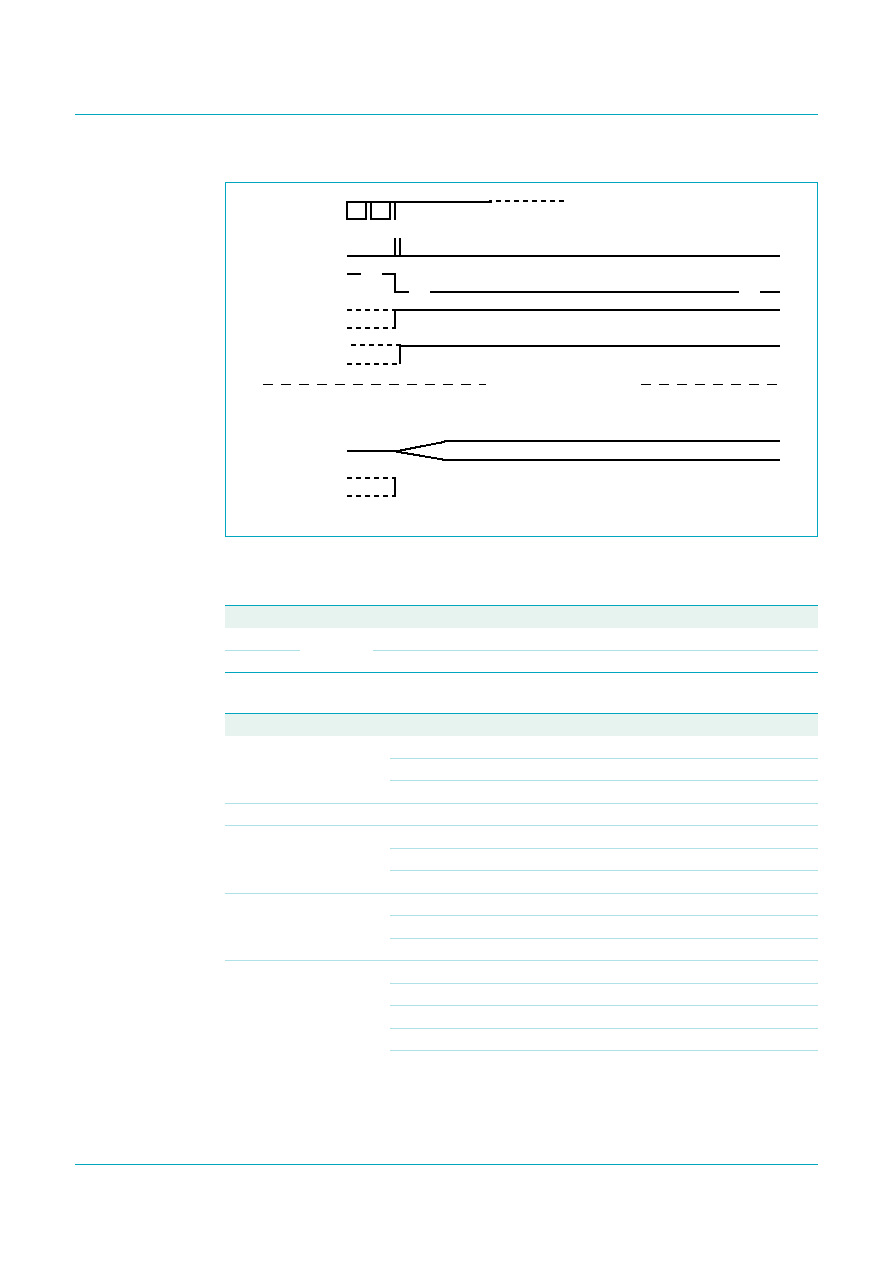
Fig 10. Search mode
Fig 11. Search mode, started during mute
001aae099
1 ms
PLL
FAST
suggested IF DSP signal control
P
I
2
C-bus
time
reset
reset
f1
f2
tuning
register SWAP
TAS read
AFHOLD
AFSAMPLE
quality detectors
tuning mute
WS processing
'00'
'01'
'10'
'11'
'11'
001aae100
PLL
P
I
2
C-bus
time
tuning
register SWAP
TAS read
AFHOLD
AFSAMPLE
f1
f2
'11'
'10'
'11'
'11'
TEF6730_1
� Koninklijke Philips Electronics N.V. 2006. All rights reserved.
Product data sheet
Rev. 01 -- 10 July 2006
19 of 56
Philips Semiconductors
TEF6730
Front-end for digital-IF car radio
Fig 12. AF update mode
Fig 13. AF update mode, started during mute
001aae101
1 ms
2 ms
0.5 ms
PLL
PLL
HOLD
suggested IF DSP signal control
P
I
2
C-bus
time
reset
f2
f1
tuning
register SWAP
TAS read
AFHOLD
AFSAMPLE
quality detectors
tuning mute
WS processing
reset
store AFU result
f1
f2
'00'
'01'
'10'
'11'
'10'
'00'
'00'
001aae102
PLL
0.5 ms
P
I
2
C-bus
time
tuning
register SWAP
TAS read
AFHOLD
AFSAMPLE
f2
f1
'11'
'10'
'00'
'00'

TEF6730_1
� Koninklijke Philips Electronics N.V. 2006. All rights reserved.
Product data sheet
Rev. 01 -- 10 July 2006
20 of 56
Philips Semiconductors
TEF6730
Front-end for digital-IF car radio
Fig 14. Jump mode
Fig 15. Jump mode, started during mute
001aae103
1 ms
0.5 ms
PLL
HOLD
suggested IF DSP signal control
P
I
2
C-bus
time
tuning
register SWAP
TAS read
AFHOLD
AFSAMPLE
quality detectors
tuning mute
WS processing
reset
f1
f2
'00'
'01'
'10'
'11'
'00'
'00'
001aae104
PLL
0.5 ms
P
I
2
C-bus
time
tuning
register SWAP
TAS read
AFHOLD
AFSAMPLE
f1
f2
'11'
'10'
'00'
'11'
'00'

TEF6730_1
� Koninklijke Philips Electronics N.V. 2006. All rights reserved.
Product data sheet
Rev. 01 -- 10 July 2006
21 of 56
Philips Semiconductors
TEF6730
Front-end for digital-IF car radio
Fig 16. Check mode
Fig 17. Check mode, started during mute
001aae105
1 ms
PLL
HOLD
suggested IF DSP signal control
P
I
2
C-bus
time
reset
f1
f2
tuning
register SWAP
TAS read
AFHOLD
AFSAMPLE
quality detectors
tuning mute
WS processing
'00'
'01'
'10'
'11'
'11'
001aae106
PLL
P
I
2
C-bus
time
tuning
register SWAP
TAS read
AFHOLD
AFSAMPLE
f1
f2
'11'
'10'
'11'
'11'
TEF6730_1
� Koninklijke Philips Electronics N.V. 2006. All rights reserved.
Product data sheet
Rev. 01 -- 10 July 2006
22 of 56
Philips Semiconductors
TEF6730
Front-end for digital-IF car radio
8.2.2 Write mode: data byte CONTROL
Fig 18. End mode
001aae107
suggested IF DSP signal control
P
I
2
C-bus
time
TAS read
AFHOLD
AFSAMPLE
quality detectors
tuning mute
WS processing
'11'
'00'
'00'
Table 14.
CONTROL - data byte 0h bit allocation with default setting
7
6
5
4
3
2
1
0
RFGAIN
0
FLAG
IFGAIN
NBAGC1
NBAGC0
DAASW
CFSW
0
0
0
0
1
0
0
Table 15.
CONTROL - data byte 0h bit description
Bit
Symbol
Description
7
RFGAIN
FM RF gain
0 = standard gain
1 = +6 dB added gain
6
-
not used, must be set to logic 0
5
FLAG
software port output open-collector
0 = SWPORT pin inactive (high-impedance)
1 = SWPORT pin active (pull-down to ground)
4
IFGAIN
IF gain
0 = standard IF gain
1 = increased IF gain (6 dB)
3 and 2
NBAGC[1:0]
RF AGC start level; setting of narrow band (IF) detection
00 = 700 mV (peak value)
01 = 560 mV (peak value)
10 = 450 mV (peak value)
11 = 350 mV (peak value)

TEF6730_1
� Koninklijke Philips Electronics N.V. 2006. All rights reserved.
Product data sheet
Rev. 01 -- 10 July 2006
23 of 56
Philips Semiconductors
TEF6730
Front-end for digital-IF car radio
8.2.3 Write mode: data byte PLLM
8.2.4 Write mode: data byte PLLL
8.2.5 Write mode: data byte DAA
1
DAASW
antenna DAA mode in FM
0 = standard; DAA output voltage is controlled by V
tune
1 = DAA output voltage is a fixed temperature stable voltage
controlled by the DAA setting (independent of V
tune
)
0
CFSW
ceramic filter switch
0 = CFSW1 pin active (low-impedance) and CFSW2 pin inactive
(high-impedance)
1 = CFSW2 pin active (low-impedance) and CFSW1 pin inactive
(high-impedance)
Table 15.
CONTROL - data byte 0h bit description
...continued
Bit
Symbol
Description
Table 16.
PLLM - data byte 1h bit allocation with default setting
7
6
5
4
3
2
1
0
CPOFF
PLL14
PLL13
PLL12
PLL11
PLL10
PLL9
PLL8
0
0
0
0
1
0
0
0
Table 17.
PLLM - data byte 1h bit description
Bit
Symbol
Description
7
CPOFF
charge pump off
0 = standard operation
1 = charge pump deactivated
6 to 0
PLL[14:8]
upper byte of PLL divider word
Table 18.
PLLL - data byte 2h bit allocation with default setting
7
6
5
4
3
2
1
0
PLL7
PLL6
PLL5
PLL4
PLL3
PLL2
PLL1
PLL0
0
1
1
1
1
1
1
0
Table 19.
PLLL - data byte 2h bit description
Bit
Symbol
Description
7 to 0
PLL[7:0]
lower byte of PLL divider word; PLL[14:0] is the divider ratio N of the
VCO programmable divider; N = 1024 to 32767
Table 20.
DAA - data byte 3h bit allocation with default setting
7
6
5
4
3
2
1
0
AGCSW
DAA6
DAA5
DAA4
DAA3
DAA2
DAA1
DAA0
0
1
0
0
0
0
0
0

TEF6730_1
� Koninklijke Philips Electronics N.V. 2006. All rights reserved.
Product data sheet
Rev. 01 -- 10 July 2006
24 of 56
Philips Semiconductors
TEF6730
Front-end for digital-IF car radio
8.2.6 Write mode: data byte AGC
Table 21.
DAA - data byte 3h bit description
Bit
Symbol
Description
7
AGCSW
RF AGC switch
0 = no drive of unused RF AGC PIN diode (FM PIN diode in
AM mode or AM PIN diode in FM mode)
1 = unused PIN diode supplied with constant current
6 to 0
DAA[6:0]
alignment of antenna circuit tuning voltage in FM mode
(0.1V
tune
to 2.0V
tune
)
Table 22.
AGC - data byte 4h bit allocation with default setting
7
6
5
4
3
2
1
0
SDAA3
SDAA2
SDAA1
SDAA0
WBAGC1
WBAGC0
KAGC
LODX
1
0
0
0
0
0
0
0
Table 23.
AGC - data byte 4h bit description
Bit
Symbol
Description
7 to 4
SDAA[3:0]
alignment of second antenna circuit tuning voltage in FM mode
(0.7V
DAAOUT1
to 1.35V
DAAOUT1
)
3 and 2
WBAGC[1:0]
RF AGC start level; setting of wideband (RF) detection; for AM,
see
Table 24
and for FM, see
Table 25
1
KAGC
FM keyed AGC
0 = keyed AGC off
1 = keyed AGC on
0
LODX
local switch
0 = standard operation (DX)
1 = forced FM RF AGC attenuation (LOCAL)
Table 24.
Setting of RF AGC threshold voltage for AM
WBAGC1
WBAGC0
AM output (RMS value) at LNAOUT
0
0
250 mV
0
1
200 mV
1
0
150 mV
1
1
70 mV
Table 25.
Setting of RF AGC threshold voltage for FM
WBAGC1
WBAGC0
FM mixer input voltage (RMS value) at FMMIXIN
0
0
24 mV
0
1
17 mV
1
0
12 mV
1
1
9 mV

TEF6730_1
� Koninklijke Philips Electronics N.V. 2006. All rights reserved.
Product data sheet
Rev. 01 -- 10 July 2006
25 of 56
Philips Semiconductors
TEF6730
Front-end for digital-IF car radio
8.2.7 Write mode: data byte BAND
The correct charge pump current for each reference frequency is selected automatically,
see
Table 30
.
Table 26.
BAND - data byte 5h bit allocation with default setting
7
6
5
4
3
2
1
0
BAND2
BAND1
BAND0
FREF2
FREF1
FREF0
LOINJ
FMIFIN
0
0
1
0
0
0
0
0
Table 27.
BAND - data byte 5h bit description
Bit
Symbol
Description
7 to 5
BAND[2:0]
see
Table 28
4 to 2
FREF[2:0]
PLL reference frequency; see
Table 29
1
LOINJ
0 = high injection image suppression
1 = low injection image suppression
0
FMIFIN
0 = FMIFAGCIN1 input is selected
1 = FMIFAGCIN2 input is selected
Table 28.
Decoding of BAND bits
BAND2
BAND1
BAND0
Divider ratio M
Receiver band
0
0
0
1
WB
0
0
1
2
FM
0
1
0
3
FM
0
1
1
6
AM
1
0
0
8
AM
1
0
1
10
AM
1
1
0
16
AM
1
1
1
20
AM
Table 29.
Reference frequencies
FREF2
FREF1
FREF0
f
ref
0
0
0
100 kHz
0
0
1
50 kHz
0
1
0
25 kHz
0
1
1
20 kHz
1
0
0
10 kHz
1
0
1
reserved
1
1
0
reserved
1
1
1
reserved

TEF6730_1
� Koninklijke Philips Electronics N.V. 2006. All rights reserved.
Product data sheet
Rev. 01 -- 10 July 2006
26 of 56
Philips Semiconductors
TEF6730
Front-end for digital-IF car radio
[1]
X = don't care.
8.2.7.1
Tuning overview
If LOINJ = 0:
.
If LOINJ = 1:
.
; where M is the divider ratio of the VCO frequency for AM mixer and
FM mixer
.
8.2.8 Write mode: data byte TEST
[1]
The test control byte is for internal use only.
Table 30.
Charge pump source
[1]
FREF2
FREF1
FREF0
LOINJ
Charge pump
current
f
ref
0
0
0
X
CP1
100 kHz
0
0
1
X
CP2
50 kHz
0
1
0
X
CP3
25 kHz
0
1
1
1
CP3
20 kHz
0
1
1
0
CP4
20 kHz
1
0
0
X
CP5
10 kHz
N
f
RF
10.7 MHz
+
(
)
M
�
f
ref
---------------------------------------------------------
=
N
f
RF
10.7 MHz
�
(
)
M
�
f
ref
---------------------------------------------------------
=
tuning step
f
ref
M
----------
=
M
f
VCO
f
mixer
---------------
=
Table 31.
Standard tuner settings
Broadcast band
BAND2 BAND1 BAND0 M
FREF2 FREF1 FREF0 f
ref
LOINJ Tuning step
Europe FM and US FM
0
0
1
2
0
0
0
100 kHz 0
50 kHz
Japan FM
0
1
0
3
0
0
0
100 kHz 1
33.3 kHz
East Europe FM (OIRT FM)
0
1
0
3
0
1
1
20 kHz
1
6.67 kHz
WB FM
0
0
0
1
0
1
0
25 kHz
0
25 kHz
AM MW and LW
1
1
1
20 0
1
1
20 kHz
0
1 kHz
AM SW 120 m to 60 m
1
1
0
16 1
0
0
10 kHz
0
0.625 kHz
AM SW 49 m to 22 m
1
0
1
10 1
0
0
10 kHz
0
1 kHz
AM SW 25 m to 15 m
1
0
0
8
1
0
0
10 kHz
0
1.25 kHz
AM SW 16 m to 11 m
0
1
1
6
1
0
0
10 kHz
0
1.67 kHz
Table 32.
TEST - data byte Fh bit allocation with default setting (not buffered)
[1]
7
6
5
4
3
2
1
0
0
0
0
0
TEST3
TEST2
TEST1
TEST0
0
0
0
0

TEF6730_1
� Koninklijke Philips Electronics N.V. 2006. All rights reserved.
Product data sheet
Rev. 01 -- 10 July 2006
27 of 56
Philips Semiconductors
TEF6730
Front-end for digital-IF car radio
9.
Limiting values
[1]
The maximum voltage must be less than V
CCA
.
[2]
Human body model: Class 2 according to JESD22-A114C.01.
[3]
Machine model: Class B according to EIA/JESD22-A115-A.
[4]
Human body model: Class 1C according to JESD22-A114C.01.
10. Thermal characteristics
Table 33.
Limiting values
In accordance with the Absolute Maximum Rating System (IEC 60134).
Symbol
Parameter
Conditions
Min
Max
Unit
V
CCA
analog supply voltage
on pins V
CC
, V
CC(PLL)
, V
CC(VCO)
, V
CC(RF)
,
V
CC(IF)
, FMMIXOUT1, FMMIXOUT2,
AMMIXOUT1 and AMMIXOUT2
-
0.3
+10
V
V
CCAn
voltage difference between
any analog supply pins
-
0.3
+0.3
V
V
SCL
voltage on pin SCL
-
0.3
+5.5
V
V
SDA
voltage on pin SDA
-
0.3
+5.5
V
V
i
input voltage
on pins ADDR1 and ADDR2
[1]
-
0.3
+5.5
V
V
o
output voltage
on pins AFHOLD and AFSAMPLE
-
0.3
+5.5
V
on pin SWPORT
-
0.3
+10
V
V
n
voltage on any other pin
-
0.3
V
CCA
+ 0.3 V
P
tot
total power dissipation
-
1100
mW
T
stg
storage temperature
-
55
+150
�
C
T
amb
ambient temperature
soldered exposed die pad
subjective functionality
-
40
+105
�
C
full functionality
-
40
+85
�
C
V
esd
electrostatic discharge
voltage
on all pins except pin V
CC(VCO)
[2]
-
2000
+2000
V
[3]
-
200
+200
V
on pin V
CC(VCO)
[4]
-
1000
+2000
V
[3]
-
200
+200
V
Table 34.
Thermal characteristics
Symbol
Parameter
Conditions
Typ
Unit
R
th(j-a)
thermal resistance from junction to ambient in free air
29.6
K/W
R
th(j-c)
thermal resistance from junction to case
17.5
K/W

TEF6730_1
� Koninklijke Philips Electronics N.V. 2006. All rights reserved.
Product data sheet
Rev. 01 -- 10 July 2006
28 of 56
Philips Semiconductors
TEF6730
Front-end for digital-IF car radio
11. Static characteristics
Table 35.
Static characteristics
V
CCA
= 8.5 V; T
amb
= 25
�
C; unless otherwise specified.
Symbol
Parameter
Conditions
Min
Typ
Max
Unit
Supply voltage
V
CCA
analog supply voltage on pins V
CC
, V
CC(PLL)
,
V
CC(VCO)
, V
CC(RF)
, V
CC(IF)
,
FMMIXOUT1,
FMMIXOUT2, AMMIXOUT1
and AMMIXOUT2
8
8.5
9
V
Current in FM mode
I
CC(RF)
RF supply current
T
amb
=
-
40
�
C
-
14
-
mA
T
amb
= 25
�
C
-
15
-
mA
T
amb
= 85
�
C
-
16
-
mA
I
CC(PLL)
PLL supply current
T
amb
=
-
40
�
C
-
7.9
-
mA
T
amb
= 25
�
C
-
7.6
-
mA
T
amb
= 85
�
C
-
7.2
-
mA
I
CC(VCO)
VCO supply current
T
amb
=
-
40
�
C
-
3.8
-
mA
T
amb
= 25
�
C
-
3.6
-
mA
T
amb
= 85
�
C
-
3.5
-
mA
I
CC
supply current
T
amb
=
-
40
�
C
-
23
-
mA
T
amb
= 25
�
C
-
21.5
-
mA
T
amb
= 85
�
C
-
19
-
mA
I
CC(IFAGC)
IF AGC supply current T
amb
=
-
40
�
C
-
26
-
mA
T
amb
= 25
�
C
-
26
-
mA
T
amb
= 85
�
C
-
26
-
mA
I
FMMIXOUT1
current on
pin FMMIXOUT1
T
amb
=
-
40
�
C
-
5.3
-
mA
T
amb
= 25
�
C
-
5.8
-
mA
T
amb
= 85
�
C
-
6.1
-
mA
I
FMMIXOUT2
current on
pin FMMIXOUT2
T
amb
=
-
40
�
C
-
5.3
-
mA
T
amb
= 25
�
C
-
5.8
-
mA
T
amb
= 85
�
C
-
6.1
-
mA
I
CC(tot)
total supply current
-
85.3
-
mA
Current in AM mode
I
CC(RF)
RF supply current
T
amb
=
-
40
�
C
-
39.5
-
mA
T
amb
= 25
�
C
-
39
-
mA
T
amb
= 85
�
C
-
38
-
mA
I
CC(PLL)
PLL supply current
T
amb
=
-
40
�
C
-
7.9
-
mA
T
amb
= 25
�
C
-
7.6
-
mA
T
amb
= 85
�
C
-
7.2
-
mA
I
CC(VCO)
VCO supply current
T
amb
=
-
40
�
C
-
3.8
-
mA
T
amb
= 25
�
C
-
3.6
-
mA
T
amb
= 85
�
C
-
3.5
-
mA

TEF6730_1
� Koninklijke Philips Electronics N.V. 2006. All rights reserved.
Product data sheet
Rev. 01 -- 10 July 2006
29 of 56
Philips Semiconductors
TEF6730
Front-end for digital-IF car radio
12. Dynamic characteristics
I
CC
supply current
T
amb
=
-
40
�
C
-
21.5
-
mA
T
amb
= 25
�
C
-
21
-
mA
T
amb
= 85
�
C
-
20
-
mA
I
CC(IFAGC)
IF AGC supply current T
amb
=
-
40
�
C
-
33
-
mA
T
amb
= 25
�
C
-
32.5
-
mA
T
amb
= 85
�
C
-
32
-
mA
I
AMMIXOUT1
current on
pin AMMIXOUT1
T
amb
=
-
40
�
C
-
6
-
mA
T
amb
= 25
�
C
-
5.5
-
mA
T
amb
= 85
�
C
-
5
-
mA
I
AMMIXOUT2
current on
pin AMMIXOUT2
T
amb
=
-
40
�
C
-
6
-
mA
T
amb
= 25
�
C
-
5.5
-
mA
T
amb
= 85
�
C
-
5
-
mA
I
CC(tot)
total supply current
-
114.7
-
mA
Table 35.
Static characteristics
...continued
V
CCA
= 8.5 V; T
amb
= 25
�
C; unless otherwise specified.
Symbol
Parameter
Conditions
Min
Typ
Max
Unit
Table 36.
Dynamic characteristics
V
CCA
= 8.5 V; T
amb
= 25
�
C; see
Figure 25
; all AC values are given in RMS; unless otherwise specified.
Symbol
Parameter
Conditions
Min
Typ
Max
Unit
Reference frequency
External reference frequency, circuit inputs: pins FREF1 and FREF2
f
ext
external frequency
-
100
-
kHz
C/N
carrier-to-noise ratio
required from reference
source; f
ext
= 100 kHz;
f = 10 kHz
115
-
-
dBc/
Hz
I
i(ext)(min)(M)
peak minimum
external input current
square wave signal
[1]
-
-
200
�
A
I
i(ext)(max)(M)
peak maximum
external input current
square wave signal
[1]
750
-
-
�
A
I
cm(ext)
external
common-mode current
from each pin to GND
-
50
-
+50
�
A
R
i
input resistance
-
5
10
V
cm
common-mode
voltage
measured between each pin to
GND
1.0
1.2
1.4
V
Tuning system; see
Table 28
,
Table 29
,
Table 30
and
Table 31
Voltage controlled oscillator
f
VCO(min)
minimum VCO
frequency
[2]
-
-
130
MHz
application according to
Figure 25
[2]
-
-
159.9
MHz
f
VCO(max)
maximum VCO
frequency
[2]
256
-
-
MHz
C/N
carrier-to-noise ratio
f
VCO
= 200 MHz;
f = 10 kHz;
Q = 30
94
98
-
dBc/
Hz

TEF6730_1
� Koninklijke Philips Electronics N.V. 2006. All rights reserved.
Product data sheet
Rev. 01 -- 10 July 2006
30 of 56
Philips Semiconductors
TEF6730
Front-end for digital-IF car radio
f
frequency deviation
caused by ripple on supply
voltage; f
ripple
= 100 Hz;
V
CC(ripple)
= 50 mV (RMS);
f
VCO
= 200 MHz; standard FM
-
2
-
Hz
Charge pump: pin CPOUT; see
Table 30
I
sink(CP1)
CP1 sink current
V
CPOUT
= 0.5 V to
V
CC(PLL)
-
1.3 V
130
180
240
�
A
I
source(CP1)
CP1 source current
V
CPOUT
= 0.5 V to
V
CC(PLL)
-
1.3 V
-
240
-
180
-
130
�
A
I
sink(CP2)
CP2 sink current
V
CPOUT
= 0.7 V to
V
CC(PLL)
-
1.5 V
270
360
480
�
A
I
source(CP2)
CP2 source current
V
CPOUT
= 0.7 V to
V
CC(PLL)
-
1.5 V
-
480
-
360
-
270
�
A
I
sink(CP3)
CP3 sink current
V
CPOUT
= 0.7 V to
V
CC(PLL)
-
0.7 V
580
780
1050
�
A
I
source(CP3)
CP3 source current
V
CPOUT
= 0.7 V to
V
CC(PLL)
-
0.7 V
-
1050
-
780
-
580
�
A
I
sink(CP4)
CP4 sink current
V
CPOUT
= 0.7 V to
V
CC(PLL)
-
0.7 V
1040
1400
1900
�
A
I
source(CP4)
CP4 source current
V
CPOUT
= 0.7 V to
V
CC(PLL)
-
0.7 V
-
1900
-
1400
-
1040
�
A
I
sink(CP5)
CP5 sink current
V
CPOUT
= 0.7 V to
V
CC(PLL)
-
0.7 V
1630
2 200
2970
�
A
I
source(CP5)
CP5 source current
V
CPOUT
= 0.7 V to
V
CC(PLL)
-
0.7 V
-
2970
-
2200
-
1630
�
A
Charge pump: pin VTUNE
I
o(sink)
output sink current
V
tune
= 0.9 V to
V
CC(PLL)
-
0.7 V
2070
2800
3780
�
A
I
o(source)
output source current
V
tune
= 0.9 V to
V
CC(PLL)
-
0.7 V
-
3780
-
2800
-
2070
�
A
Timings
t
tune
tuning time
Europe FM and US FM band;
f
ref
= 100 kHz; f
RF
= 87.5 MHz
to 108 MHz
-
0.75
1
ms
AM MW band; f
ref
= 20 kHz;
f
RF
= 0.53 MHz to 1.7 MHz
-
-
10
ms
t
upd(AF)
AF update time
cycle time for inaudible AF
update including 1 ms mute
start and 1 ms mute release
time
-
6
6.5
ms
Antenna Digital Auto Alignment (DAA)
DAA1: pin DAAOUT1
[3]
G
conv(DAA)
DAA conversion gain
0.1
-
2
Table 36.
Dynamic characteristics
...continued
V
CCA
= 8.5 V; T
amb
= 25
�
C; see
Figure 25
; all AC values are given in RMS; unless otherwise specified.
Symbol
Parameter
Conditions
Min
Typ
Max
Unit

TEF6730_1
� Koninklijke Philips Electronics N.V. 2006. All rights reserved.
Product data sheet
Rev. 01 -- 10 July 2006
31 of 56
Philips Semiconductors
TEF6730
Front-end for digital-IF car radio
V
o
output voltage
FM mode; DAASW = 0
minimum value
-
-
0.6
V
maximum value
V
CC(PLL)
-
0.6 -
-
V
FM mode; DAASW = 1;
independent of tuning voltage
minimum value; data byte
DAA bits
DAA[6:0] = 000 0000
-
-
0.6
V
maximum value; data byte
DAA bits
DAA[6:0] = 111 1111
V
CC(PLL)
-
0.6 -
-
V
AM mode; independent of
tuning voltage
minimum value; data byte
DAA bits
DAA[6:0] = 000 0000
-
-
0.6
V
maximum value; data byte
DAA bits
DAA[6:0] = 111 1111
V
CC(PLL)
-
0.6 -
-
V
V
n(o)
output noise voltage
data byte DAA bits
DAA[6:0] = 100 0000;
FM mode; V
tune
= 4 V with
frequency range from
300 Hz to 22 kHz
-
30
100
�
V
V
o(T)
output voltage
deviation over
temperature
T
amb
=
-
40
�
C to +85
�
C; data
byte DAA bits
DAA[6:0] = 100 0000
-
30
-
+30
mV
V
o(step)
step output voltage
tolerance
n = 0 to 127; FM mode;
V
tune
= 4 V
-
0.5V
LSB
0
+0.5V
LSB
V
o
output voltage
deviation
V
tune
= 4 V; I
load
= 50
�
A
-
V
LSB
-
+V
LSB
V
tune
= 4 V; I
load
=
-
50
�
A
-
V
LSB
-
+V
LSB
t
s(o)
output settling time
V
DAAOUT1
= 0.2 V to 8.25 V;
C
L
= 270 pF
-
30
60
�
s
ripple
ripple rejection
V
CC(ripple)
/V
o
; data byte DAA
bits DAA[6:0] = 101 0101;
FM mode; V
tune
= 4 V;
f
ripple
= 100 Hz;
V
CC(ripple)
= 100 mV
-
40
-
dB
DAA2: pin DAAOUT2
[4]
G
conv(DAA)
DAA conversion gain
0.7
-
1.35
V
o
output voltage
AM mode and FM mode
minimum value
-
-
0.6
V
maximum value
V
CC(PLL)
-
0.8 -
-
V
V
n(o)
output noise voltage
data byte AGC bits
SDAA[3:0] = 1000; FM mode;
V
DAAOUT1
= 4 V with frequency
range from 300 Hz to 22 kHz
-
30
100
�
V
Table 36.
Dynamic characteristics
...continued
V
CCA
= 8.5 V; T
amb
= 25
�
C; see
Figure 25
; all AC values are given in RMS; unless otherwise specified.
Symbol
Parameter
Conditions
Min
Typ
Max
Unit

TEF6730_1
� Koninklijke Philips Electronics N.V. 2006. All rights reserved.
Product data sheet
Rev. 01 -- 10 July 2006
32 of 56
Philips Semiconductors
TEF6730
Front-end for digital-IF car radio
V
o(T)
output voltage
deviation over
temperature
T
amb
=
-
40
�
C to +85
�
C; data
byte AGC bits
SDAA[3:0] = 1000
-
30
-
+30
mV
V
o(step)
step output voltage
tolerance
n = 0 to 15; FM mode;
V
DAAOUT1
= 4 V
-
0.5V
LSB
0
+0.5V
LSB
V
o
output voltage
deviation
V
DAAOUT1
= 4 V; I
load
= 50
�
A
-
V
LSB
-
+V
LSB
V
DAAOUT1
= 4 V; I
load
=
-
50
�
A
-
V
LSB
-
+V
LSB
t
s(o)
output settling time
V
DAAOUT1
= 4 V;
V
DAAOUT2
= 2.8 V to 5.4 V;
C
L
= 270 pF
-
20
30
�
s
ripple
ripple rejection
V
CC(ripple)
/V
DAAOUT1
; data byte
AGC bits SDAA[3:0] = 1010;
FM mode; V
DAAOUT1
= 4 V;
f
ripple
= 100 Hz;
V
CC(ripple)
= 100 mV
-
50
-
dB
AM channel
AM RF AGC wideband detector (average detector): pin LNAOUT
V
LNAOUT(RMS)
RMS voltage on
pin LNAOUT
start level of wideband AGC;
R
L
= 430
(load at
pin LNAOUT); m = 0.3;
see
Table 24
and
Table 25
data byte AGC bits
WBAGC[1:0] = 00
175
250
350
mV
data byte AGC bits
WBAGC[1:0] = 01
140
200
280
mV
data byte AGC bits
WBAGC[1:0] = 10
105
150
210
mV
data byte AGC bits
WBAGC[1:0] = 11
49
70
98
mV
AM RF AGC narrow-band detector: pins IFOUT1 and IFOUT2
V
o(IFOUT)(M)
peak output voltage
between pin IFOUT1
and pin IFOUT2
start level of narrow-band
AGC; data byte CONTROL bit
IFGAIN = 0;
V
IFAGCMSB
= HIGH;
V
IFAGCLSB
= LOW;
see
Table 15
data byte CONTROL bits
NBAGC[1:0] = 00
490
700
980
mV
data byte CONTROL bits
NBAGC[1:0] = 01
390
560
780
mV
data byte CONTROL bits
NBAGC[1:0] = 10
315
450
630
mV
data byte CONTROL bits
NBAGC[1:0] = 11
245
350
490
mV
AM LNA and AGC
Input: pin LNAIN; output: pin LNAOUT
R
i
input resistance
0.9
1.3
1.8
M
Table 36.
Dynamic characteristics
...continued
V
CCA
= 8.5 V; T
amb
= 25
�
C; see
Figure 25
; all AC values are given in RMS; unless otherwise specified.
Symbol
Parameter
Conditions
Min
Typ
Max
Unit

TEF6730_1
� Koninklijke Philips Electronics N.V. 2006. All rights reserved.
Product data sheet
Rev. 01 -- 10 July 2006
33 of 56
Philips Semiconductors
TEF6730
Front-end for digital-IF car radio
C
i
input capacitance
-
46
69
pF
G
m
transconductance gain I
o
/V
i
40
57
81
mA/V
G
m(T)
transconductance gain
deviation over
temperature
T
amb
=
-
40
�
C to +85
�
C;
see
Figure 19
-
-
-
dB
IP3
third-order intercept
point
R
L
= 430
(load at
pin LNAOUT)
111
114
-
dB
�
V
IP2
second-order intercept
point
R
L
= 430
(load at
pin LNAOUT)
120
129
-
dB
�
V
V
n(i)(eq)
equivalent input noise
voltage
C
source
= 110 pF; R
L
= 430
(load at pin LNAOUT)
f
RF
= 1 MHz
-
1.0
1.4
nV/
Hz
f
RF
= 144 kHz
-
2.3
3.2
nV/
Hz
R
o
output resistance
80
115
165
C
o
output capacitance
in series with output resistance
-
22
33
pF
V
o(p-p)(max)
maximum
peak-to-peak output
voltage
-
2.2
-
V
G
AGC
AGC gain range
8
11
14
dB
RF PIN diode AGC current generator output: pin IAMAGC
G
AGC
AGC gain range
f
RF
= 1 MHz; dummy aerial
15 pF/60 pF
-
50
-
dB
V
IAMAGC
voltage on
pin IAMAGC
PIN diode drive DC voltage
2.2
-
V
CCA
V
I
sink(max)
maximum sink current
V
IAMAGC
= 2.2 V
[5]
10
-
-
mA
I
sink
sink current
FM mode; data byte DAA bit
AGCSW = 1
0.6
0.9
1.4
mA
FM mode; data byte DAA bit
AGCSW = 0
-
-
100
nA
AM mixer (IF = 10.7 MHz)
Mixer input: pins AMMIXIN and AMMIXDEC
R
i
input resistance
[6]
40
-
-
k
C
i
input capacitance
[6]
-
3
4.5
pF
V
i(max)
maximum input
voltage
on pin AMMIXIN; 1 dB
compression point of
V
MIXOUT1-MIXOUT2
; m = 0
500
-
-
mV
Mixer output: pins AMMIXOUT1 and AMMIXOUT2
R
o
output resistance
[7]
100
-
-
k
C
o
output capacitance
[7]
-
4
7
pF
V
o(p-p)(max)
maximum
peak-to-peak output
voltage
12
15
-
V
G
m(conv)
conversion
transconductance gain
I
o
/V
i
1.8
2.4
3.2
mA/V
Table 36.
Dynamic characteristics
...continued
V
CCA
= 8.5 V; T
amb
= 25
�
C; see
Figure 25
; all AC values are given in RMS; unless otherwise specified.
Symbol
Parameter
Conditions
Min
Typ
Max
Unit

TEF6730_1
� Koninklijke Philips Electronics N.V. 2006. All rights reserved.
Product data sheet
Rev. 01 -- 10 July 2006
34 of 56
Philips Semiconductors
TEF6730
Front-end for digital-IF car radio
G
m(conv)(T)
conversion
transconductance gain
deviation over
temperature
T
amb
=
-
40
�
C to +85
�
C;
see
Figure 20
-
-
-
dB
IP3
third-order intercept
point
R
L
= 2.6 k
(AC load between
output pins);
f = 300 kHz
135
138
-
dB
�
V
IP2
second-order intercept
point
R
L
= 2.6 k
(AC load between
output pins)
-
170
-
dB
�
V
V
n(i)(eq)
equivalent input noise
voltage
band limited noise;
R
source
= 750
; noise of
R
source
included; R
L
= 2.6 k
(AC load between output pins)
-
7.2
10
nV/
Hz
NF
noise figure
-
6.2
9
dB
FM channel
FM RF AGC (FM distance mode; data byte AGC bit LODX = 0)
Input: pins FMMIXIN1 and FMMIXIN2
[8]
V
i(FMMIXIN)(RMS)
RMS input voltage
between
pin FMMIXIN1 and
pin FMMIXIN2
start level of wideband AGC;
keyed AGC off; data byte AGC
bit KAGC = 0; see
Table 24
and
Table 25
data byte AGC bits
WBAGC[1:0] = 11
5
9
15
mV
data byte AGC bits
WBAGC[1:0] = 10
7
12
19
mV
data byte AGC bits
WBAGC[1:0] = 01
10
17
27
mV
data byte AGC bits
WBAGC[1:0] = 00
14
24
38
mV
start level of wideband AGC;
keyed AGC on; data byte AGC
bit KAGC = 1;
V
KAGC
> V
th(KAGC)
data byte AGC bits
WBAGC[1:0] = 11
19
30
48
mV
data byte AGC bits
WBAGC[1:0] = 10
21
33
52
mV
data byte AGC bits
WBAGC[1:0] = 01
24
38
60
mV
data byte AGC bits
WBAGC[1:0] = 00
28
45
71
mV
Table 36.
Dynamic characteristics
...continued
V
CCA
= 8.5 V; T
amb
= 25
�
C; see
Figure 25
; all AC values are given in RMS; unless otherwise specified.
Symbol
Parameter
Conditions
Min
Typ
Max
Unit

TEF6730_1
� Koninklijke Philips Electronics N.V. 2006. All rights reserved.
Product data sheet
Rev. 01 -- 10 July 2006
35 of 56
Philips Semiconductors
TEF6730
Front-end for digital-IF car radio
FM RF AGC narrow-band detector: pins IFOUT1 and IFOUT2
V
o(IFOUT)(M)
peak output voltage
between pin IFOUT1
and pin IFOUT2
start level of narrow-band
AGC; data byte CONTROL bit
IFGAIN = 0;
V
IFAGCMSB
= HIGH;
V
IFAGCLSB
= LOW;
see
Table 15
data byte CONTROL bits
NBAGC[1:0] = 00
490
700
980
mV
data byte CONTROL bits
NBAGC[1:0] = 01
390
560
780
mV
data byte CONTROL bits
NBAGC[1:0] = 10
315
450
630
mV
data byte CONTROL bits
NBAGC[1:0] = 11
245
350
490
mV
PIN diode drive output: pin IFMAGC
I
source(max)
maximum source
current
V
TFMAGC
= V
IFMAGC
+ 1.4 V;
data byte AGC bit KAGC = 0
-
16
-
10
-
7
mA
I
sink(max)
maximum sink current
at AGC decay;
V
TFMAGC
= V
IFMAGC
; data byte
AGC bit KAGC = 0
7
10
16
mA
I
source
source current
AM mode; data byte DAA bit
AGCSW = 1
-
-
1.2
-
mA
AM mode; data byte DAA bit
AGCSW = 0
-
0
-
mA
data byte AGC bit LODX = 1
(FM local)
-
0.75
-
0.5
-
0.35
mA
V
IFMAGC
voltage on
pin IFMAGC
voltage at PIN diode drive
output; V
FMMIXIN1
< V
th
-
100
300
mV
V
th(KAGC)
threshold voltage on
pin KAGC
threshold level voltage for
narrow-band AGC (keyed
AGC); data byte AGC bit
KAGC = 1; see
Table 15
and
Table 23
500
950
1400
mV
FM mixer (IF = 10.7 MHz)
FM RF input: pins FMMIXIN1 and FMMIXIN2
[8]
V
i(RF)(max)
maximum RF input
voltage
1 dB compression point of
FM mixer output voltage
75
100
-
mV
V
n(i)(eq)
equivalent input noise
voltage
R
source
= 500
; noise of
R
source
included; R
L
= 2.6 k
(on output pins FMMIXOUT1
and FMMIXOUT2)
RFGAIN = 0
-
3.7
5.2
nV/
Hz
RFGAIN = 1
-
3
-
nV/
Hz
R
i
input resistance
RFGAIN = 0
3
3.8
4.7
k
RFGAIN = 1
1.6
2.0
2.5
k
Table 36.
Dynamic characteristics
...continued
V
CCA
= 8.5 V; T
amb
= 25
�
C; see
Figure 25
; all AC values are given in RMS; unless otherwise specified.
Symbol
Parameter
Conditions
Min
Typ
Max
Unit

TEF6730_1
� Koninklijke Philips Electronics N.V. 2006. All rights reserved.
Product data sheet
Rev. 01 -- 10 July 2006
36 of 56
Philips Semiconductors
TEF6730
Front-end for digital-IF car radio
C
i
input capacitance
-
2
4
pF
G
m(conv)
conversion
transconductance gain
I
o
/V
i
; RF gain 1; data byte
PLLM bit RFGAIN = 0
12
18
25
mA/V
I
o
/V
i
; RF gain 2; data byte
PLLM bit RFGAIN = 1
24
36
50
mA/V
G
m(conv)(T)
conversion
transconductance gain
deviation over
temperature
T
amb
=
-
40
�
C to +85
�
C;
see
Figure 21
-
-
-
dB
NF
noise figure
R
source
= 500
; T
amb
= 25
�
C
RFGAIN = 0
-
3.5
5
dB
RFGAIN = 1
-
3
4.5
dB
IP3
third-order intercept
point
RFGAIN = 0
117
123
-
dB
�
V
RFGAIN = 1
108
114
-
dB
�
V
IRR
image rejection ratio
V
o(wanted)
/V
o(image)
;
f
RF(wanted)
= 87.5 MHz;
f
RF(image)
= 108.9 MHz
25
40
-
dB
Output: pins FMMIXOUT1 and FMMIXOUT2
[9]
R
o
output resistance
100
-
-
k
C
o
output capacitance
-
4
6
pF
V
o(p-p)(max)
maximum
peak-to-peak output
voltage
4.5
5.6
-
V
FM weather band input: pins WXMIXIN and WXMIXDEC
G
m(conv)
conversion
transconductance gain
I
o
/V
i
10
15
21
mA/V
G
m(conv)(T)
conversion
transconductance gain
deviation over
temperature
T
amb
=
-
40
�
C to +85
�
C;
see
Figure 22
-
-
-
dB
R
i
input resistance
-
5.1
-
k
C
i
input capacitance
-
2
4
pF
NF
noise figure
R
source
= 300
-
3.5
5
dB
IP3
third-order intercept
point
-
116
-
dB
�
V
IRR
image rejection ratio
V
o(wanted)
/V
o(image)
;
f
RF(wanted)
= 162.475 MHz;
f
RF(image)
= 183.875 MHz
20
33
-
dB
IF AGC amplifier
AM mode; inputs: pins AMIFAGCIN and IFAGCDEC
[10]
; outputs: pins IFOUT1 and IFOUT2
[11]
R
i
input resistance
-
100
-
k
C
i
input capacitance
-
5
7
pF
R
o
output resistance
120
210
290
Table 36.
Dynamic characteristics
...continued
V
CCA
= 8.5 V; T
amb
= 25
�
C; see
Figure 25
; all AC values are given in RMS; unless otherwise specified.
Symbol
Parameter
Conditions
Min
Typ
Max
Unit

TEF6730_1
� Koninklijke Philips Electronics N.V. 2006. All rights reserved.
Product data sheet
Rev. 01 -- 10 July 2006
37 of 56
Philips Semiconductors
TEF6730
Front-end for digital-IF car radio
G
gain
data byte CONTROL bit
IFGAIN = 0
V
IFAGCMSB
= LOW;
V
IFAGCLSB
= LOW
21.2
24.2
27.2
dB
V
IFAGCMSB
= LOW;
V
IFAGCLSB
= HIGH
15.2
18.2
21.2
dB
V
IFAGCMSB
= HIGH;
V
IFAGCLSB
= HIGH
9.2
12.2
15.2
dB
V
IFAGCMSB
= HIGH;
V
IFAGCLSB
= LOW
3.2
6.2
9.2
dB
data byte CONTROL bit
IFGAIN = 1
V
IFAGCMSB
= LOW;
V
IFAGCLSB
= LOW
27.2
30.2
33.2
dB
V
IFAGCMSB
= LOW;
V
IFAGCLSB
= HIGH
21.2
24.2
27.2
dB
V
IFAGCMSB
= HIGH;
V
IFAGCLSB
= HIGH
15.2
18.2
21.2
dB
V
IFAGCMSB
= HIGH;
V
IFAGCLSB
= LOW
9.2
12.2
15.2
dB
NF
noise figure
R
source
= 300
; data byte
CONTROL bit IFGAIN = 0;
V
IFAGCMSB
= LOW;
V
IFAGCLSB
= LOW
-
12.9
16
dB
IM3
third-order
intermodulation
distance
two output signals at 35 kHz
frequency distance; differential
output level of 200 mV; data
byte CONTROL bit IFGAIN = 0
V
IFAGCMSB
= LOW;
V
IFAGCLSB
= LOW
77
83
-
dB
V
IFAGCMSB
= LOW;
V
IFAGCLSB
= HIGH
77
83
-
dB
V
IFAGCMSB
= HIGH;
V
IFAGCLSB
= HIGH
77
83
-
dB
V
IFAGCMSB
= HIGH;
V
IFAGCLSB
= LOW
74
80
-
dB
Table 36.
Dynamic characteristics
...continued
V
CCA
= 8.5 V; T
amb
= 25
�
C; see
Figure 25
; all AC values are given in RMS; unless otherwise specified.
Symbol
Parameter
Conditions
Min
Typ
Max
Unit

TEF6730_1
� Koninklijke Philips Electronics N.V. 2006. All rights reserved.
Product data sheet
Rev. 01 -- 10 July 2006
38 of 56
Philips Semiconductors
TEF6730
Front-end for digital-IF car radio
V
i(max)(M)
peak maximum input
voltage
1 dB compression point of
IF AGC amplifier output
voltage; data byte CONTROL
bit IFGAIN = 0
V
IFAGCMSB
= LOW;
V
IFAGCLSB
= LOW
45
-
-
mV
V
IFAGCMSB
= LOW;
V
IFAGCLSB
= HIGH
90
-
-
mV
V
IFAGCMSB
= HIGH;
V
IFAGCLSB
= HIGH
180
-
-
mV
V
IFAGCMSB
= HIGH;
V
IFAGCLSB
= LOW
360
-
-
mV
FM mode; inputs: pins FMIFAGCIN1 and IFAGCDEC
[12]
; outputs: pins IFOUT1 and IFOUT2
[11]
R
i
input resistance
-
330
-
C
i
input capacitance
-
5
7
pF
R
o
output resistance
120
210
290
G
gain
data byte CONTROL bit
IFGAIN = 0
V
IFAGCMSB
= LOW;
V
IFAGCLSB
= LOW
28
31
34
dB
V
IFAGCMSB
= LOW;
V
IFAGCLSB
= HIGH
22
25
28
dB
V
IFAGCMSB
= HIGH;
V
IFAGCLSB
= HIGH
16
19
22
dB
V
IFAGCMSB
= HIGH;
V
IFAGCLSB
= LOW
10
13
16
dB
data byte CONTROL bit
IFGAIN = 1
V
IFAGCMSB
= LOW;
V
IFAGCLSB
= LOW
34
37
40
dB
V
IFAGCMSB
= LOW;
V
IFAGCLSB
= HIGH
28
31
34
dB
V
IFAGCMSB
= HIGH;
V
IFAGCLSB
= HIGH
22
25
28
dB
V
IFAGCMSB
= HIGH;
V
IFAGCLSB
= LOW
16
19
22
dB
NF
noise figure
R
source
= 300
; data byte
CONTROL bit IFGAIN = 0;
V
IFAGCMSB
= LOW;
V
IFAGCLSB
= LOW
-
6.9
8.5
dB
IP3
third-order intercept
point
data byte CONTROL bit
IFGAIN = 0
110
115
-
dB
�
V
Table 36.
Dynamic characteristics
...continued
V
CCA
= 8.5 V; T
amb
= 25
�
C; see
Figure 25
; all AC values are given in RMS; unless otherwise specified.
Symbol
Parameter
Conditions
Min
Typ
Max
Unit

TEF6730_1
� Koninklijke Philips Electronics N.V. 2006. All rights reserved.
Product data sheet
Rev. 01 -- 10 July 2006
39 of 56
Philips Semiconductors
TEF6730
Front-end for digital-IF car radio
V
i(max)(M)
peak maximum input
voltage
1 dB compression point of
IF AGC amplifier output
voltage; data byte CONTROL
bit IFGAIN = 0
V
IFAGCMSB
= LOW;
V
IFAGCLSB
= LOW
20
-
-
mV
V
IFAGCMSB
= LOW;
V
IFAGCLSB
= HIGH
40
-
-
mV
V
IFAGCMSB
= HIGH;
V
IFAGCLSB
= HIGH
80
-
-
mV
V
IFAGCMSB
= HIGH;
V
IFAGCLSB
= LOW
160
-
-
mV
FM mode; inputs: pins FMIFAGCIN2 and IFAGCDEC
[13]
; outputs: pins IFOUT1 and IFOUT2
[11]
R
i
input resistance
-
330
-
C
i
input capacitance
-
5
7
pF
G
gain
data byte CONTROL bit
IFGAIN = 0
V
IFAGCMSB
= LOW;
V
IFAGCLSB
= LOW
28
31
34
dB
V
IFAGCMSB
= LOW;
V
IFAGCLSB
= HIGH
22
25
28
dB
V
IFAGCMSB
= HIGH;
V
IFAGCLSB
= HIGH
16
19
22
dB
V
IFAGCMSB
= HIGH;
V
IFAGCLSB
= LOW
10
13
16
dB
data byte CONTROL bit
IFGAIN = 1
V
IFAGCMSB
= LOW;
V
IFAGCLSB
= LOW
34
37
40
dB
V
IFAGCMSB
= LOW;
V
IFAGCLSB
= HIGH
28
31
34
dB
V
IFAGCMSB
= HIGH;
V
IFAGCLSB
= HIGH
22
25
28
dB
V
IFAGCMSB
= HIGH;
V
IFAGCLSB
= LOW
16
19
22
dB
NF
noise figure
R
source
= 300
; data byte
CONTROL bit IFGAIN = 0;
V
IFAGCMSB
= LOW;
V
IFAGCLSB
= LOW
-
6.9
8.5
dB
IP3
third-order intercept
point
data byte CONTROL bit
IFGAIN = 0
110
115
-
dB
�
V
Table 36.
Dynamic characteristics
...continued
V
CCA
= 8.5 V; T
amb
= 25
�
C; see
Figure 25
; all AC values are given in RMS; unless otherwise specified.
Symbol
Parameter
Conditions
Min
Typ
Max
Unit

TEF6730_1
� Koninklijke Philips Electronics N.V. 2006. All rights reserved.
Product data sheet
Rev. 01 -- 10 July 2006
40 of 56
Philips Semiconductors
TEF6730
Front-end for digital-IF car radio
[1]
Differential current on pins FREF1 and FREF2.
[2]
The VCO frequency is determined by the external circuit at pins OSCFDB and OSCTNK.
[3]
Conversion gain formula of DAA1:
where n = 0 to 127.
[4]
Conversion gain formula of DAA2:
where n = 0 to 15.
[5]
The sink current must be limited to 18 mA by the external circuit.
[6]
Input parameters of AM mixer measured between pins AMMIXIN and AMMIXDEC.
[7]
Output parameters of AM mixer measured between pins AMMIXOUT1 and AMMIXOUT2.
[8]
Input parameters of FM mixer measured between pins FMMIXIN1 and FMMIXIN2.
[9]
Output parameters of FM mixer measured between pins FMMIXOUT1 and FMMIXOUT2.
[10] Input parameters of AM IF amplifier measured between pins AMIFAGCIN and IFAGCDEC.
[11] Output parameters of IF AGC amplifier measured between pins IFOUT1 and IFOUT2.
[12] Input parameters of FM IF amplifier measured between pins FMIFAGCIN1 and IFAGCDEC.
[13] Input parameters of FM IF amplifier measured between pins FMIFAGCIN2 and IFAGCDEC.
V
i(max)(M)
peak maximum input
voltage
1 dB compression point of
IF AGC amplifier output
voltage; data byte CONTROL
bit IFGAIN = 0
V
IFAGCMSB
= LOW;
V
IFAGCLSB
= LOW
20
-
-
mV
V
IFAGCMSB
= LOW;
V
IFAGCLSB
= HIGH
40
-
-
mV
V
IFAGCMSB
= HIGH;
V
IFAGCLSB
= HIGH
80
-
-
mV
V
IFAGCMSB
= HIGH;
V
IFAGCLSB
= LOW
160
-
-
mV
Digital inputs and outputs
Input: pins IFAGCMSB and IFAGCLSB
V
IL
LOW-level input
voltage
-
-
0.9
V
V
IH
HIGH-level input
voltage
1.5
-
-
V
Output: pin AFHOLD
I
sink(max)
maximum sink current
AFHOLD = LOW; V
o
= 0.4 V
1.0
-
-
mA
Output: pin AFSAMPLE
I
sink(max)
maximum sink current
AFSAMPLE = LOW;
V
o
= 0.4 V
1.0
-
-
mA
Output: pin SWPORT
I
sink(max)
maximum sink current
data byte CONTROL bit
FLAG = 1; V
o
= 0.4 V
1.0
-
-
mA
Table 36.
Dynamic characteristics
...continued
V
CCA
= 8.5 V; T
amb
= 25
�
C; see
Figure 25
; all AC values are given in RMS; unless otherwise specified.
Symbol
Parameter
Conditions
Min
Typ
Max
Unit
V
DAAOUT 1
1.915
n
128
---------
�
0.1
+
V
tune
�
=
V
DAAOUT 2
0.693
n
16
------
�
0.7
+
V
DAAOUT 1
�
=

TEF6730_1
� Koninklijke Philips Electronics N.V. 2006. All rights reserved.
Product data sheet
Rev. 01 -- 10 July 2006
41 of 56
Philips Semiconductors
TEF6730
Front-end for digital-IF car radio
13. I
2
C-bus characteristics
The TEF6730HW complies with the fast-mode I
2
C-bus protocol. The maximum I
2
C-bus
communication speed is 400 kbit/s.
SDA and SCL HIGH and LOW internal thresholds are specified according to an I
2
C-bus
voltage range from 2.5 V to 3.3 V including I
2
C-bus voltage tolerances of
�
10 %. The
I
2
C-bus interface tolerates also SDA and SCL signals from a 5 V bus. Restrictions for V
IL
in a 5 V application can be derived from
Table 37
.
Fig 19. AM LNA transconductance gain deviation over
temperature (including application)
Fig 20. AM mixer conversion transconductance gain
deviation over temperature (including
application)
001aae090
T
amb
(
�
C)
-
40
100
80
0
40
0
-
1
1
2
G
m(T)
(dB)
-
2
001aae091
T
amb
(
�
C)
-
40
100
80
0
40
0
-
0.5
0.5
1.0
-
1.0
G
m(conv)(T)
(dB)
Fig 21. FM mixer conversion transconductance gain
deviation over temperature (including
application)
Fig 22. Weather band mixer conversion
transconductance gain deviation over
temperature (including application)
001aae092
T
amb
(
�
C)
-
40
100
80
0
40
-
0.5
-
1.0
0
0.5
-
1.5
G
m(conv)(T)
(dB)
001aae093
T
amb
(
�
C)
-
40
100
80
0
40
0
-
5
5
10
-
10
G
m(conv)(T)
(dB)
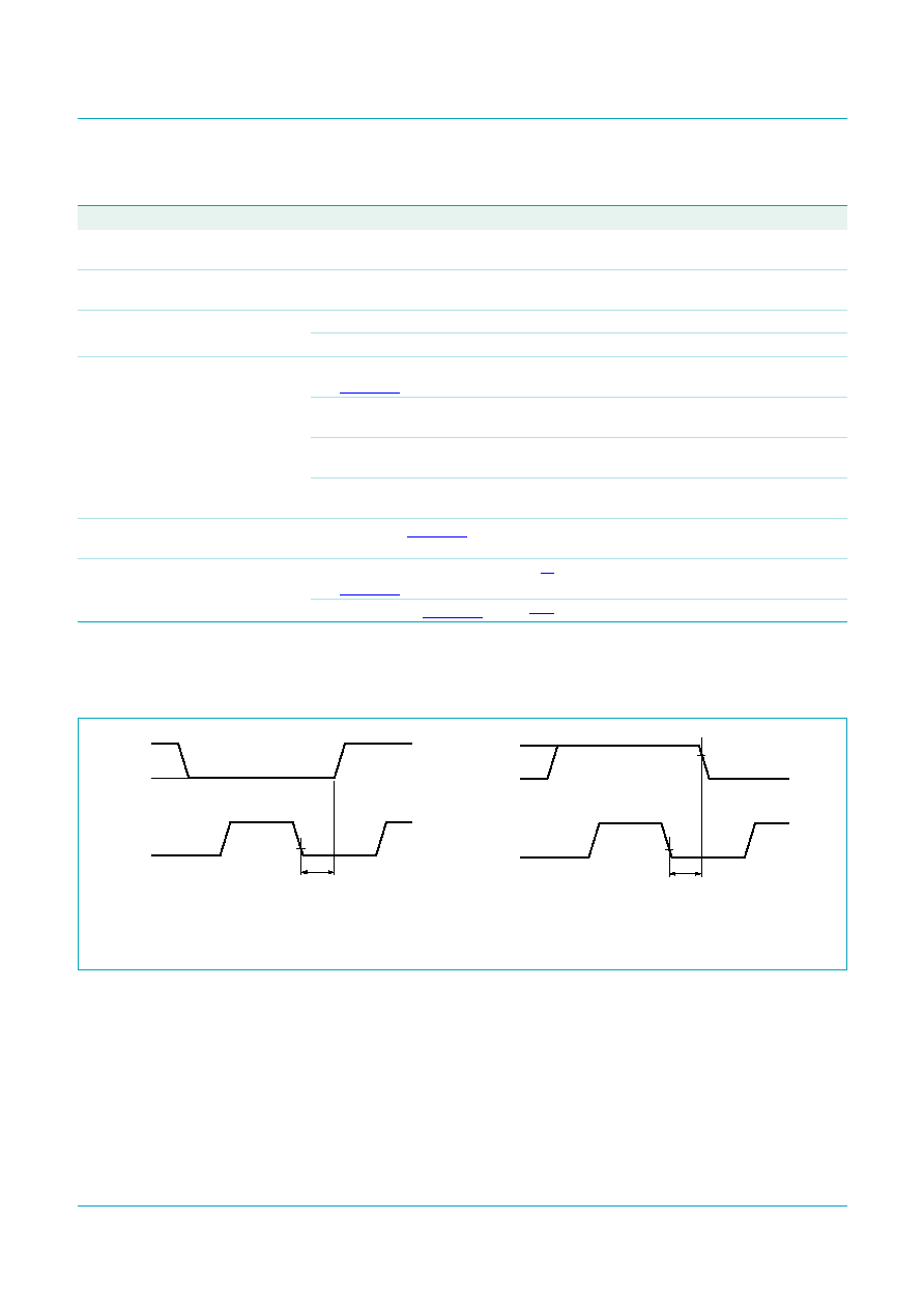
TEF6730_1
� Koninklijke Philips Electronics N.V. 2006. All rights reserved.
Product data sheet
Rev. 01 -- 10 July 2006
42 of 56
Philips Semiconductors
TEF6730
Front-end for digital-IF car radio
[1]
Minimum value of t
of
; C
b
= total capacitance of one I
2
C-bus line [pF].
[2]
Typical value of t
of
; the output fall time t
of
[ns] depends on the total load capacitance C
b
[pF] and the I
2
C-bus voltage V
DD
[V]:
t
of
=
1
/
12
�
V
DD
�
C
b
.
Table 37.
I
2
C-bus parameters
Symbol
Parameter
Conditions
Min
Typ
Max
Unit
V
IL
LOW-level input
voltage
-
-
1.09
V
V
IH
HIGH-level input
voltage
1.56
-
-
V
C
i
capacitance for each
I/O pin
pin SDA
-
4
6
pF
pin SCL
-
3
5
pF
t
resp(Q)HL
HIGH-to-LOW data
output response time
acknowledge and read data;
see
Figure 23
V
DD
= 5 V; I = 3 mA;
C
b
= 400 pF
-
700
863
ns
V
DD
= 3.3 V; R
p
= 1.8 k
;
C
b
= 400 pF
-
570
668
ns
V
DD
= 2.5 V; R
p
= 35 k
;
C
b
= 10 pF
-
520
593
ns
t
resp(Q)LH
LOW-to-HIGH data
output response time
read data; see
Figure 23
-
450
488
ns
t
of
output fall time from
V
IHmin
to V
ILmax
C
b
= 10 pF to 120 pF;
see
Figure 24
[1]
20 + 0.1C
b
10
�
V
DD
-
ns
C
b
120 pF; see
Figure 24
[1][2]
20 + 0.1C
b
-
250
ns
a. Data change from LOW to HIGH
b. Data change from HIGH to LOW
Fig 23. Data output response time of the IC
001aaf002
SDA
SCL
V
IL(max)
t
resp(Q)LH
001aaf001
V
IL(max)
0.7V
DD
t
resp(Q)HL

TEF6730_1
� Koninklijke Philips Electronics N.V. 2006. All rights reserved.
Product data sheet
Rev. 01 -- 10 July 2006
43 of 56
Philips Semiconductors
TEF6730
Front-end for digital-IF car radio
14. Overall system parameters
Fig 24. Definition of the fall time of the output signal
001aab803
V
DD
0.7V
DD
0.3V
DD
t
of
Table 38.
Overall system parameters
V
CCA
= 8.5 V; T
amb
= 25
�
C; see
Figure 25
; all AC values are given in RMS; unless otherwise specified.
Symbol
Parameter
Conditions
Min
Typ
Max
Unit
AM overall system parameters
[1]
f
i(RF)
RF input frequency
LW
144
-
288
kHz
MW
522
-
1710
kHz
SW
2.3
-
26.1
MHz
f
IF
IF frequency
-
10.7
-
MHz
V
sens
sensitivity voltage
(S+N)/N = 26 dB
-
50
-
�
V
V
i(RF)
RF input voltage
start level of wideband AGC
data byte AGC bits WBAGC[1:0] = 00
-
125
-
mV
data byte AGC bits WBAGC[1:0] = 01
-
100
-
mV
data byte AGC bits WBAGC[1:0] = 10
-
75
-
mV
data byte AGC bits WBAGC[1:0] = 11
-
35
-
mV
V
i(RF)M
peak RF input voltage
start level of narrow-band AGC; m = 0
data byte AGC bits NBAGC[1:0] = 00
-
200
-
mV
data byte AGC bits NBAGC[1:0] = 01
-
170
-
mV
data byte AGC bits NBAGC[1:0] = 10
-
140
-
mV
data byte AGC bits NBAGC[1:0] = 11
-
115
-
mV
IP2
second-order intercept point referenced to receiver input
-
152
-
dB
�
V
IP3
third-order intercept point
referenced to receiver input
f = 40 kHz
-
130
-
dB
�
V
f = 100 kHz
-
133
-
dB
�
V
ripple
ripple rejection
V
CC(ripple)
/V
audio
; f
ripple
= 100 Hz;
V
CC(ripple)
= 10 mV (RMS);
V
i(RF)
= 1 mV to 1 V
-
40
-
dB
FM overall system parameters
[2]
f
i(RF)
RF input frequency
FM standard
65
-
108
MHz
weather band
162.4 -
162.55 MHz
f
IF
IF frequency
-
10.7
-
MHz

TEF6730_1
� Koninklijke Philips Electronics N.V. 2006. All rights reserved.
Product data sheet
Rev. 01 -- 10 July 2006
44 of 56
Philips Semiconductors
TEF6730
Front-end for digital-IF car radio
[1]
Based on 15 pF/60 pF dummy aerial, voltages at dummy aerial input, f
mod
= 400 Hz, 2.5 kHz audio bandwidth, f
i(RF)
= 990 kHz, m = 0.3
and nominal maximum IF AGC gain, unless otherwise specified.
[2]
Based on 75
dummy aerial, voltages at dummy aerial input, f
mod
= 400 Hz, de-emphasis = 50
�
s, f
i(RF)
= 97.1 MHz,
f = 22.5 kHz,
nominal mixer gain and nominal maximum IF AGC gain, unless otherwise specified.
V
sens
sensitivity voltage
B
IF
= 170 kHz
-
2
-
�
V
threshold extension enabled; weak signal
handling enabled (SAF7730 N231)
-
1.1
-
�
V
V
i(RF)
RF input voltage
start level of wideband AGC
data byte AGC bits WBAGC[1:0] = 00
-
19
-
mV
data byte AGC bits WBAGC[1:0] = 01
-
14
-
mV
data byte AGC bits WBAGC[1:0] = 10
-
10
-
mV
data byte AGC bits WBAGC[1:0] = 11
-
7
-
mV
V
i(RF)M
peak RF input voltage
start level of narrow-band AGC; m = 0
data byte AGC bits NBAGC[1:0] = 00
-
17
-
mV
data byte AGC bits NBAGC[1:0] = 01
-
14
-
mV
data byte AGC bits NBAGC[1:0] = 10
-
11
-
mV
data byte AGC bits NBAGC[1:0] = 11
-
9
-
mV
IP3
third-order intercept point
f = 400 kHz
-
123
-
dB
�
V
ripple
ripple rejection
V
CC(ripple)
/V
audio
; f
ripple
= 100 Hz;
V
CC(ripple)
= 10 mV (RMS); V
i(RF)
= 500
�
V
-
64
-
dB
Table 38.
Overall system parameters
...continued
V
CCA
= 8.5 V; T
amb
= 25
�
C; see
Figure 25
; all AC values are given in RMS; unless otherwise specified.
Symbol
Parameter
Conditions
Min
Typ
Max
Unit

xxxx xxxxxxxxxxxxxxxxxxxxxxxxxxxxxx x xxxxxxxxxxxxxx xxxxxxxxxx xxx xxxxxx xxxxxxxxxxxxxxxxxxxxxxx xxxxxxxxxxxxxxxxxxxxxx
xxxxx xxxxxx xx xxxxxxxxxxxxxxxxxxxxxxxxxxxxx xxxxxxxxxxxxxxxxxxxxxx xxxxxxxxxxx xxxxxxx xxxxxxxxxxxxxxxxxxx
xxxxxxxxxxxxxxxx xxxxxxxxxxxxxx xxxxxx xx xxxxxxxxxxxxxxxxxxxxxxxxxxxxxxxx xxxxxxxxxxxxxxxxxxxxxxxx xxxxxxx
xxxxxxxxxxxxxxxxxxxxxxxxxxxxxxxxxxxxxxxxxxxxxx xxxxxxxxxxx xxxxx x x
TEF6730_1
� K
oninklijk
e Philips Electronics N.V
. 2006. All r
ights reser
v
ed.
Pr
oduct data sheet
Re
v
.
01 -- 10 J
u
l
y
2006
45 of 56
Philips Semiconductor
s
TEF6730
Fr
ont-end f
or digital-IF car radio
15.
Application inf
ormation
(1) For list of components see
Table 39
.
Fig 25. Application diagram of TEF6730HW
001aae108
100 nF
C1
270 pF
D1
BB208
D2
BB207
L1
50 nH
L2
100
nH
3.9
nF
33
pF
4.7 pF
3.3 nF
100 nF
1
nF
10 pF
1 nF
1 nF
22 nF
10.7 MHz
F1
22
nF
1
�
F
100 nF
100 nF
100
nF
1
�
F
220 nF
1 nF
100 nF
120 pF
1
nF
L6
18 pF
220
pF
D3
BAP70-02
D4
BAP70-02
D5
BAP70AM
6.8
�
H
10 k
2.2 k
1.2 k
22 k
470 k
82
2.2 k
1 nF
100
nF
330
2.2 M
430
10 k
470 k
560
6.8 pF
3.3
�
H
22 nF
47
�
F
100 nF
6.8 pF
4.7 k
22
L3
470 nH
390
�
H
680
�
H
L4
220 nH
L5
47 mH
ifagc
FM
ifagc
ifagc
V
P
V
P
V
P
V
P
lna rf
lna
rf
62
63
64
1
2
3
4
5
7
8
10 9
11
12
13
14
15
17
19
20
21
22
23
24
25
31
34
KEYED
AGC
30
26
27
28
29
32
33
35
36
39
40
37
38
41
53
54
55
56
57
45
52
16, 18, 48, 49
43
42
44
46
47
address
selection
50
51
58
59
60
61
6
antenna DAA
TEF6730HW
AM RF
AGC
FM RF
AGC
BAND
�
M
REF
f
ref
PLL
�
N
IF AGC
AM LNA
IFOUT1
am/fm
rf agc
IFOUT2
IFAGCMSB
IFAGCLSB
SDA
AFSAMPLE
AFHOLD
SCL
VCO
VCO
V
P
V
P
FREF
sup
sup
V
P
+8.5 V
fgnd
dig
i.c.
flag
pll
90
�
WX
90
�
1.8 nF
1 nF
10 nF
47
�
H
1 nF
TUNING
STATE
MACHINE
I
2
C-BUS
tuner
control
CTRL
BUF
read
address
pll in-lock
write
MIXER
MIXER
MIXER
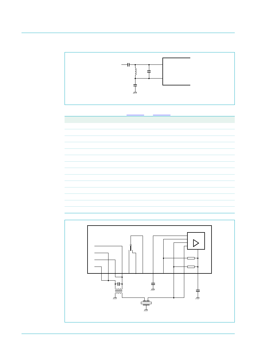
TEF6730_1
� Koninklijke Philips Electronics N.V. 2006. All rights reserved.
Product data sheet
Rev. 01 -- 10 July 2006
46 of 56
Philips Semiconductors
TEF6730
Front-end for digital-IF car radio
Fig 26. Weather band application
Table 39.
List of components of
Figure 25
and
Figure 26
Symbol Component
Type
Manufacturer
C1
capacitor for VCO tuning
270 pF; type NP0
-
L1
VCO coil
50 nH; E558CNA-100035 TOKO
L2
FM input coil
100 nH; C2520C-R10
Sagami
L3
FM antenna coil
470 nH; C2520C-R47
Sagami
L4
FM antenna coil
220 nH; C2520C-R22
Sagami
L5
AM mains suppression coil
47 mH; 388BN-1211Z
TOKO
L6
10.7 MHz IF coil
PF670CCS-A065DX
TOKO
L7
weather band input coil
47 nH; LQW31H
MURATA
D1
VCO variable capacitance diode
BB208
Philips
D2
FM RF selectivity variable capacitance diode BB207
Philips
D3
FM PIN diode
BAP70-02
Philips
D4
FM PIN diode
BAP70-02
Philips
D5
AM PIN diode
BAP70AM
Philips
F1
10.7 MHz IF ceramic filter
SFELA10M7HAA0-B0
MURATA
Fig 27. FM and AM mode
001aae109
10 pF
10 pF
12 pF
L7
47 nH
28
RF input
29
TEF6730HW
001aae110
22 nF
22 nF
330
330
AM
FM
10
11
9
8
7
6
5
4
3
2
1
64
TEF6730HW
IF AGC
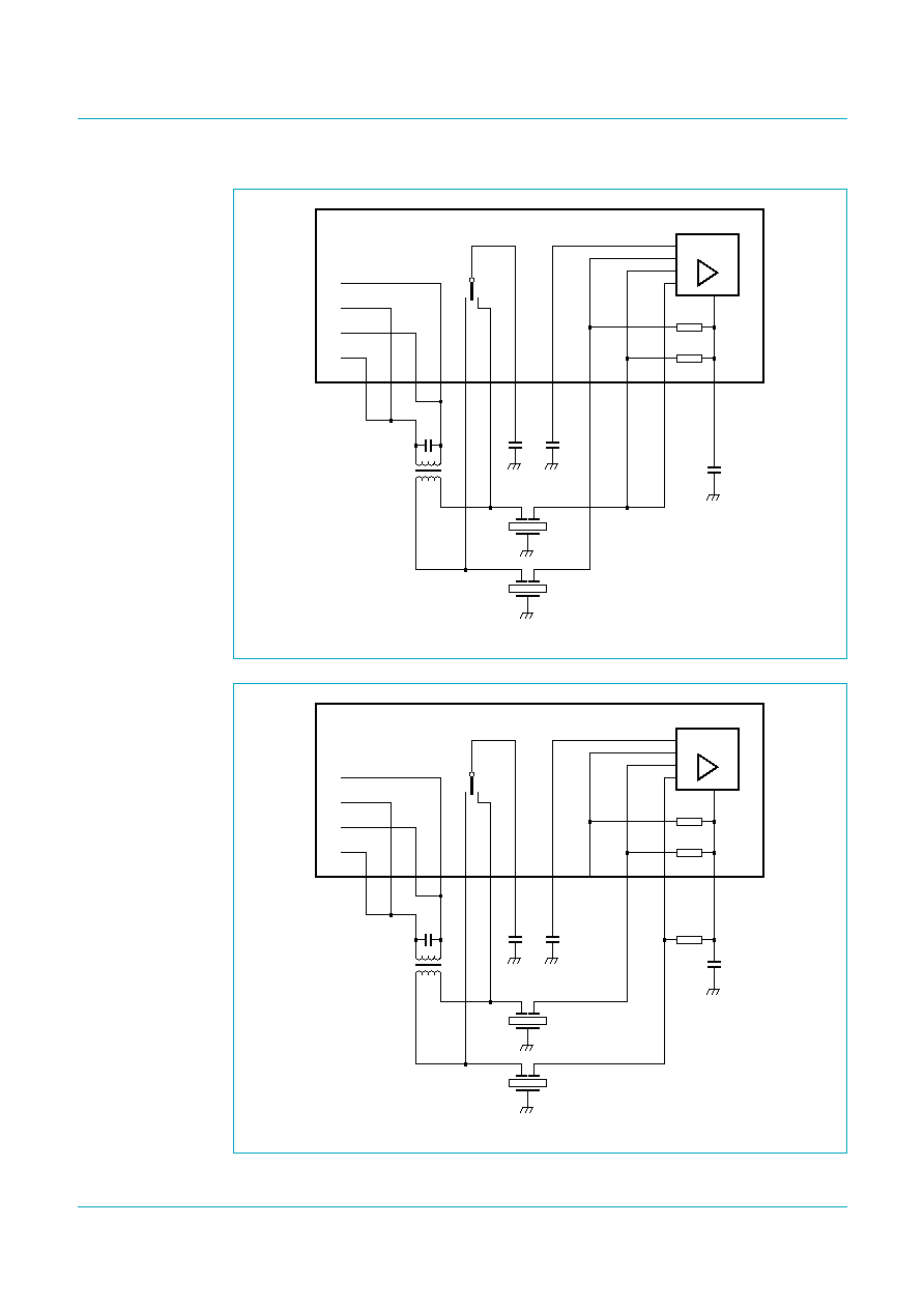
TEF6730_1
� Koninklijke Philips Electronics N.V. 2006. All rights reserved.
Product data sheet
Rev. 01 -- 10 July 2006
47 of 56
Philips Semiconductors
TEF6730
Front-end for digital-IF car radio
Fig 28. FM/AM and FM HD mode
Fig 29. FM and AM (narrow band) mode
001aae111
10
nF
22
nF
22 nF
330
330
AM
FM
10
11
9
8
7
6
5
4
3
2
1
64
TEF6730HW
IF AGC
FM HD
FM/AM
001aae112
10
nF
22 nF
22 nF
330
330
330
AM
FM
10
11
9
8
7
6
5
4
3
2
1
64
TEF6730HW
IF AGC
AM
FM

TEF6730_1
� Koninklijke Philips Electronics N.V. 2006. All rights reserved.
Product data sheet
Rev. 01 -- 10 July 2006
48 of 56
Philips Semiconductors
TEF6730
Front-end for digital-IF car radio
Fig 30. FM, AM, AM HD and FM HD mode
001aae113
10
nF
22
nF
22 nF
330
330
330
AM
FM
10
11
9
8
7
6
5
4
3
2
1
64
TEF6730HW
IF AGC
FM HD
AM and AM HD
FM

TEF6730_1
� Koninklijke Philips Electronics N.V. 2006. All rights reserved.
Product data sheet
Rev. 01 -- 10 July 2006
49 of 56
Philips Semiconductors
TEF6730
Front-end for digital-IF car radio
16. Package outline
Fig 31. Package outline SOT855-1 (HTQFP64)
REFERENCES
OUTLINE
VERSION
EUROPEAN
PROJECTION
ISSUE DATE
IEC
JEDEC
JEITA
SOT855-1
MS-026
SOT855-1
04-05-18
05-05-11
Note
1. Plastic or metal protrusions of 0.25 mm maximum per side are not included
DIMENSIONS (mm are the original dimensions)
HTQFP64: plastic thermal enhanced thin quad flat package; 64 leads; body 10 x 10 x 1 mm; exposed die pad
0
5
10 mm
scale
64
17
49
32
1
16
48
33
b
p
b
p
D
H
D
E
H
E
B
A
D
h
E
h
Z
D
Z
E
e
e
w
M
w
M
v
B
M
v
A
M
UNIT
A
max
mm
1.2
0.12
0.05
1.05
0.95
0.27
0.17
0.18
0.12
10.1
9.9
10.1
9.9
12.15
11.85
12.15
11.85
0.75
0.45
1.45
1.05
1.45
1.05
A
1
A
2
A
3
0.25
b
p
c
D
(1)
E
(1)
e
0.5
H
D
4.7
4.5
D
h
4.7
4.5
E
h
H
E
L
1
L
p
v
0.2
w
0.08
y
0.1
Z
D
(1)
Z
E
(1)
7
�
0
�
y
c
exposed die pad
A
L
p
detail X
L
(A
3
)
A
2
A
1
pin 1
index
X

TEF6730_1
� Koninklijke Philips Electronics N.V. 2006. All rights reserved.
Product data sheet
Rev. 01 -- 10 July 2006
50 of 56
Philips Semiconductors
TEF6730
Front-end for digital-IF car radio
17. Soldering
17.1 Introduction to soldering surface mount packages
There is no soldering method that is ideal for all surface mount IC packages. Wave
soldering can still be used for certain surface mount ICs, but it is not suitable for fine pitch
SMDs. In these situations reflow soldering is recommended.
17.2 Reflow soldering
Reflow soldering requires solder paste (a suspension of fine solder particles, flux and
binding agent) to be applied to the printed-circuit board by screen printing, stencilling or
pressure-syringe dispensing before package placement. Driven by legislation and
environmental forces the worldwide use of lead-free solder pastes is increasing.
Several methods exist for reflowing; for example, convection or convection/infrared
heating in a conveyor type oven. Throughput times (preheating, soldering and cooling)
vary between 100 seconds and 200 seconds depending on heating method.
Typical reflow temperatures range from 215
�
C to 260
�
C depending on solder paste
material. The peak top-surface temperature of the packages should be kept below:
Moisture sensitivity precautions, as indicated on packing, must be respected at all times.
17.3 Wave soldering
Conventional single wave soldering is not recommended for surface mount devices
(SMDs) or printed-circuit boards with a high component density, as solder bridging and
non-wetting can present major problems.
To overcome these problems the double-wave soldering method was specifically
developed.
If wave soldering is used the following conditions must be observed for optimal results:
�
Use a double-wave soldering method comprising a turbulent wave with high upward
pressure followed by a smooth laminar wave.
�
For packages with leads on two sides and a pitch (e):
Table 40.
SnPb eutectic process - package peak reflow temperatures (from
J-STD-020C
July 2004)
Package thickness
Volume mm
3
< 350
Volume mm
3
350
< 2.5 mm
240
�
C + 0/
-
5
�
C
225
�
C + 0/
-
5
�
C
2.5 mm
225
�
C + 0/
-
5
�
C
225
�
C + 0/
-
5
�
C
Table 41.
Pb-free process - package peak reflow temperatures (from
J-STD-020C July
2004)
Package thickness
Volume mm
3
< 350
Volume mm
3
350 to
2000
Volume mm
3
> 2000
< 1.6 mm
260
�
C + 0
�
C
260
�
C + 0
�
C
260
�
C + 0
�
C
1.6 mm to 2.5 mm
260
�
C + 0
�
C
250
�
C + 0
�
C
245
�
C + 0
�
C
2.5 mm
250
�
C + 0
�
C
245
�
C + 0
�
C
245
�
C + 0
�
C

TEF6730_1
� Koninklijke Philips Electronics N.V. 2006. All rights reserved.
Product data sheet
Rev. 01 -- 10 July 2006
51 of 56
Philips Semiconductors
TEF6730
Front-end for digital-IF car radio
� larger than or equal to 1.27 mm, the footprint longitudinal axis is preferred to be
parallel to the transport direction of the printed-circuit board;
� smaller than 1.27 mm, the footprint longitudinal axis must be parallel to the
transport direction of the printed-circuit board.
The footprint must incorporate solder thieves at the downstream end.
�
For packages with leads on four sides, the footprint must be placed at a 45
�
angle to
the transport direction of the printed-circuit board. The footprint must incorporate
solder thieves downstream and at the side corners.
During placement and before soldering, the package must be fixed with a droplet of
adhesive. The adhesive can be applied by screen printing, pin transfer or syringe
dispensing. The package can be soldered after the adhesive is cured.
Typical dwell time of the leads in the wave ranges from 3 seconds to 4 seconds at 250
�
C
or 265
�
C, depending on solder material applied, SnPb or Pb-free respectively.
A mildly-activated flux will eliminate the need for removal of corrosive residues in most
applications.
17.4 Manual soldering
Fix the component by first soldering two diagonally-opposite end leads. Use a low voltage
(24 V or less) soldering iron applied to the flat part of the lead. Contact time must be
limited to 10 seconds at up to 300
�
C.
When using a dedicated tool, all other leads can be soldered in one operation within
2 seconds to 5 seconds between 270
�
C and 320
�
C.
17.5 Package related soldering information
[1]
For more detailed information on the BGA packages refer to the
(LF)BGA Application Note (AN01026);
order a copy from your Philips Semiconductors sales office.
[2]
All surface mount (SMD) packages are moisture sensitive. Depending upon the moisture content, the
maximum temperature (with respect to time) and body size of the package, there is a risk that internal or
external package cracks may occur due to vaporization of the moisture in them (the so called popcorn
effect). For details, refer to the Drypack information in the
Data Handbook IC26; Integrated Circuit
Packages; Section: Packing Methods.
Table 42.
Suitability of surface mount IC packages for wave and reflow soldering methods
Package
[1]
Soldering method
Wave
Reflow
[2]
BGA, HTSSON..T
[3]
, LBGA, LFBGA, SQFP,
SSOP..T
[3]
, TFBGA, VFBGA, XSON
not suitable
suitable
DHVQFN, HBCC, HBGA, HLQFP, HSO, HSOP,
HSQFP, HSSON, HTQFP, HTSSOP, HVQFN,
HVSON, SMS
not suitable
[4]
suitable
PLCC
[5]
, SO, SOJ
suitable
suitable
LQFP, QFP, TQFP
not recommended
[5][6]
suitable
SSOP, TSSOP, VSO, VSSOP
not recommended
[7]
suitable
CWQCCN..L
[8]
, PMFP
[9]
, WQCCN..L
[8]
not suitable
not suitable

TEF6730_1
� Koninklijke Philips Electronics N.V. 2006. All rights reserved.
Product data sheet
Rev. 01 -- 10 July 2006
52 of 56
Philips Semiconductors
TEF6730
Front-end for digital-IF car radio
[3]
These transparent plastic packages are extremely sensitive to reflow soldering conditions and must on no
account be processed through more than one soldering cycle or subjected to infrared reflow soldering with
peak temperature exceeding 217
�
C
�
10
�
C measured in the atmosphere of the reflow oven. The package
body peak temperature must be kept as low as possible.
[4]
These packages are not suitable for wave soldering. On versions with the heatsink on the bottom side, the
solder cannot penetrate between the printed-circuit board and the heatsink. On versions with the heatsink
on the top side, the solder might be deposited on the heatsink surface.
[5]
If wave soldering is considered, then the package must be placed at a 45
�
angle to the solder wave
direction. The package footprint must incorporate solder thieves downstream and at the side corners.
[6]
Wave soldering is suitable for LQFP, QFP and TQFP packages with a pitch (e) larger than 0.8 mm; it is
definitely not suitable for packages with a pitch (e) equal to or smaller than 0.65 mm.
[7]
Wave soldering is suitable for SSOP, TSSOP, VSO and VSSOP packages with a pitch (e) equal to or larger
than 0.65 mm; it is definitely not suitable for packages with a pitch (e) equal to or smaller than 0.5 mm.
[8]
Image sensor packages in principle should not be soldered. They are mounted in sockets or delivered
pre-mounted on flex foil. However, the image sensor package can be mounted by the client on a flex foil by
using a hot bar soldering process. The appropriate soldering profile can be provided on request.
[9]
Hot bar soldering or manual soldering is suitable for PMFP packages.

TEF6730_1
� Koninklijke Philips Electronics N.V. 2006. All rights reserved.
Product data sheet
Rev. 01 -- 10 July 2006
53 of 56
Philips Semiconductors
TEF6730
Front-end for digital-IF car radio
18. Footprint for soldering
Fig 32. Footprint
0.500
0.285
(56
�
)
0.1425
(8
�
)
0.400
(3
�
)
0.400 (3
�
)
7.900 (4
�
)
10.250 (2
�
)
12.400 (2
�
)
13.650 (2
�
)
12.200 (2
�
)
10.400 (4
�
)
9.035 (4
�
)
4.700
(2
�
)
4.800
(2
�
)
solder land
solder paste deposit
solder land plus solder paste
placement area
occupied area
0.285
(8
�
)
SOT855-1
Dimensions in mm

TEF6730_1
� Koninklijke Philips Electronics N.V. 2006. All rights reserved.
Product data sheet
Rev. 01 -- 10 July 2006
54 of 56
Philips Semiconductors
TEF6730
Front-end for digital-IF car radio
19. Abbreviations
20. Revision history
Table 43.
Abbreviations
Acronym
Description
ADC
Analog-to-Digital Converter
AF
Alternative Frequency
AFU
Alternative Frequency Updating
AGC
Automatic Gain Control
DAA
Digital Auto Alignment
DSP
Digital Signal Processor
DX
Distance
HD
High Definition
IF
Intermediate Frequency
LNA
Low Noise Amplifier
LO
Local Oscillator
LSB
Least Significant Bit
LW
Long Wave
MSB
Most Significant Bit
MW
Medium Wave
PLL
Phase-Locked Loop
RF
Radio Frequency
SCL
Serial Clock
SDA
Serial Data
SW
Short Wave
VCO
Voltage-Controlled Oscillator
WB
Weather Band
Table 44.
Revision history
Document ID
Release date
Data sheet status
Change notice
Supersedes
TEF6730_1
20060710
Product data sheet
-
-

TEF6730_1
� Koninklijke Philips Electronics N.V. 2006. All rights reserved.
Product data sheet
Rev. 01 -- 10 July 2006
55 of 56
Philips Semiconductors
TEF6730
Front-end for digital-IF car radio
21. Legal information
21.1
Data sheet status
[1]
Please consult the most recently issued document before initiating or completing a design.
[2]
The term `short data sheet' is explained in section "Definitions".
[3]
The product status of device(s) described in this document may have changed since this document was published and may differ in case of multiple devices. The latest product status
information is available on the Internet at URL
http://www.semiconductors.philips.com.
21.2
Definitions
Draft -- The document is a draft version only. The content is still under
internal review and subject to formal approval, which may result in
modifications or additions. Philips Semiconductors does not give any
representations or warranties as to the accuracy or completeness of
information included herein and shall have no liability for the consequences of
use of such information.
Short data sheet -- A short data sheet is an extract from a full data sheet
with the same product type number(s) and title. A short data sheet is intended
for quick reference only and should not be relied upon to contain detailed and
full information. For detailed and full information see the relevant full data
sheet, which is available on request via the local Philips Semiconductors
sales office. In case of any inconsistency or conflict with the short data sheet,
the full data sheet shall prevail.
21.3
Disclaimers
General -- Information in this document is believed to be accurate and
reliable. However, Philips Semiconductors does not give any representations
or warranties, expressed or implied, as to the accuracy or completeness of
such information and shall have no liability for the consequences of use of
such information.
Right to make changes -- Philips Semiconductors reserves the right to
make changes to information published in this document, including without
limitation specifications and product descriptions, at any time and without
notice. This document supersedes and replaces all information supplied prior
to the publication hereof.
Suitability for use -- Philips Semiconductors products are not designed,
authorized or warranted to be suitable for use in medical, military, aircraft,
space or life support equipment, nor in applications where failure or
malfunction of a Philips Semiconductors product can reasonably be expected
to result in personal injury, death or severe property or environmental
damage. Philips Semiconductors accepts no liability for inclusion and/or use
of Philips Semiconductors products in such equipment or applications and
therefore such inclusion and/or use is at the customer's own risk.
Applications -- Applications that are described herein for any of these
products are for illustrative purposes only. Philips Semiconductors makes no
representation or warranty that such applications will be suitable for the
specified use without further testing or modification.
Limiting values -- Stress above one or more limiting values (as defined in
the Absolute Maximum Ratings System of IEC 60134) may cause permanent
damage to the device. Limiting values are stress ratings only and operation of
the device at these or any other conditions above those given in the
Characteristics sections of this document is not implied. Exposure to limiting
values for extended periods may affect device reliability.
Terms and conditions of sale -- Philips Semiconductors products are sold
subject to the general terms and conditions of commercial sale, as published
at
http://www.semiconductors.philips.com/profile/terms
, including those
pertaining to warranty, intellectual property rights infringement and limitation
of liability, unless explicitly otherwise agreed to in writing by Philips
Semiconductors. In case of any inconsistency or conflict between information
in this document and such terms and conditions, the latter will prevail.
No offer to sell or license -- Nothing in this document may be interpreted
or construed as an offer to sell products that is open for acceptance or the
grant, conveyance or implication of any license under any copyrights, patents
or other industrial or intellectual property rights.
21.4
Trademarks
Notice: All referenced brands, product names, service names and trademarks
are the property of their respective owners.
I
2
C-bus -- logo is a trademark of Koninklijke Philips Electronics N.V.
22. Contact information
For additional information, please visit: http://www.semiconductors.philips.com
For sales office addresses, send an email to: sales.addresses@www.semiconductors.philips.com
Document status
[1][2]
Product status
[3]
Definition
Objective [short] data sheet
Development
This document contains data from the objective specification for product development.
Preliminary [short] data sheet
Qualification
This document contains data from the preliminary specification.
Product [short] data sheet
Production
This document contains the product specification.

Philips Semiconductors
TEF6730
Front-end for digital-IF car radio
� Koninklijke Philips Electronics N.V. 2006.
All rights reserved.
For more information, please visit: http://www.semiconductors.philips.com.
For sales office addresses, email to: sales.addresses@www.semiconductors.philips.com.
Date of release: 10 July 2006
Document identifier: TEF6730_1
Please be aware that important notices concerning this document and the product(s)
described herein, have been included in section `Legal information'.
23. Contents
1
General description . . . . . . . . . . . . . . . . . . . . . . 1
2
Features . . . . . . . . . . . . . . . . . . . . . . . . . . . . . . . 1
3
Quick reference data . . . . . . . . . . . . . . . . . . . . . 2
4
Ordering information . . . . . . . . . . . . . . . . . . . . . 4
5
Block diagram . . . . . . . . . . . . . . . . . . . . . . . . . . 5
6
Pinning information . . . . . . . . . . . . . . . . . . . . . . 6
6.1
Pinning . . . . . . . . . . . . . . . . . . . . . . . . . . . . . . . 6
6.2
Pin description . . . . . . . . . . . . . . . . . . . . . . . . . 6
7
Functional description . . . . . . . . . . . . . . . . . . . 8
7.1
FM mixer 1 . . . . . . . . . . . . . . . . . . . . . . . . . . . . 8
7.2
FM RF AGC . . . . . . . . . . . . . . . . . . . . . . . . . . . 8
7.3
Antenna DAA1 and DAA2. . . . . . . . . . . . . . . . . 8
7.4
AM LNA . . . . . . . . . . . . . . . . . . . . . . . . . . . . . . 9
7.5
AM RF AGC . . . . . . . . . . . . . . . . . . . . . . . . . . . 9
7.6
AM mixer. . . . . . . . . . . . . . . . . . . . . . . . . . . . . . 9
7.7
VCO and dividers . . . . . . . . . . . . . . . . . . . . . . . 9
7.8
Tuning PLL . . . . . . . . . . . . . . . . . . . . . . . . . . . . 9
7.9
AM/FM IF AGC amplifier. . . . . . . . . . . . . . . . . . 9
8
I
2
C-bus protocol . . . . . . . . . . . . . . . . . . . . . . . . . 9
8.1
Read mode . . . . . . . . . . . . . . . . . . . . . . . . . . . 10
8.1.1
Read mode: data byte TUNER . . . . . . . . . . . . 10
8.1.2
Read mode: data byte ID . . . . . . . . . . . . . . . . 11
8.2
Write mode . . . . . . . . . . . . . . . . . . . . . . . . . . . 11
8.2.1
Mode and subaddress byte for write. . . . . . . . 16
8.2.2
Write mode: data byte CONTROL . . . . . . . . . 22
8.2.3
Write mode: data byte PLLM . . . . . . . . . . . . . 23
8.2.4
Write mode: data byte PLLL . . . . . . . . . . . . . . 23
8.2.5
Write mode: data byte DAA . . . . . . . . . . . . . . 23
8.2.6
Write mode: data byte AGC . . . . . . . . . . . . . . 24
8.2.7
Write mode: data byte BAND . . . . . . . . . . . . . 25
8.2.7.1
Tuning overview . . . . . . . . . . . . . . . . . . . . . . . 26
8.2.8
Write mode: data byte TEST . . . . . . . . . . . . . 26
9
Limiting values. . . . . . . . . . . . . . . . . . . . . . . . . 27
10
Thermal characteristics. . . . . . . . . . . . . . . . . . 27
11
Static characteristics. . . . . . . . . . . . . . . . . . . . 28
12
Dynamic characteristics . . . . . . . . . . . . . . . . . 29
13
I
2
C-bus characteristics . . . . . . . . . . . . . . . . . . 41
14
Overall system parameters . . . . . . . . . . . . . . . 43
15
Application information. . . . . . . . . . . . . . . . . . 45
16
Package outline . . . . . . . . . . . . . . . . . . . . . . . . 49
17
Soldering . . . . . . . . . . . . . . . . . . . . . . . . . . . . . 50
17.1
Introduction to soldering surface mount
packages . . . . . . . . . . . . . . . . . . . . . . . . . . . . 50
17.2
Reflow soldering . . . . . . . . . . . . . . . . . . . . . . . 50
17.3
Wave soldering . . . . . . . . . . . . . . . . . . . . . . . . 50
17.4
Manual soldering . . . . . . . . . . . . . . . . . . . . . . 51
17.5
Package related soldering information . . . . . . 51
18
Footprint for soldering . . . . . . . . . . . . . . . . . . 53
19
Abbreviations . . . . . . . . . . . . . . . . . . . . . . . . . 54
20
Revision history . . . . . . . . . . . . . . . . . . . . . . . 54
21
Legal information . . . . . . . . . . . . . . . . . . . . . . 55
21.1
Data sheet status . . . . . . . . . . . . . . . . . . . . . . 55
21.2
Definitions . . . . . . . . . . . . . . . . . . . . . . . . . . . 55
21.3
Disclaimers. . . . . . . . . . . . . . . . . . . . . . . . . . . 55
21.4
Trademarks . . . . . . . . . . . . . . . . . . . . . . . . . . 55
22
Contact information . . . . . . . . . . . . . . . . . . . . 55
23
Contents. . . . . . . . . . . . . . . . . . . . . . . . . . . . . . 56