
DATA SHEET
Preliminary specification
File under Integrated Circuits, IC01
May 1991
INTEGRATED CIRCUITS
TEA6360
5-band stereo equalizer circuit

May 1991
2
Philips Semiconductors
Preliminary specification
5-band stereo equalizer circuit
TEA6360
FEATURES
À
Monolithic integrated 5-band stereo equalizer circuit
À
Five filters for each channel
À
Centre frequency, bandwidth and maximum boost/cut
defined by external components
À
Choise for variable or constant Q-factor via I
2
C software
À
Defeat mode
À
All stages are DC-coupled
À
I
2
C-bus control for all functions
À
Two different modul addresses programmable.
GENERAL DESCRIPTION
The 5-band stereo equalizer is an 1
2
C-bus controlled tone
processor for application in car radio sets, TV sets and
music centres. It offers the possibility of sound control as
well as equalization of sound pressure behaviour of
different rooms or loudspeakers, especially in cars.
QUICK REFERENCE DATA
ORDERING INFORMATION
Notes
1. SOT232; SOT232-1; 1996 August 08.
2. SOT287; SOT287-1; 1996 August 08.
SYMBOL
PARAMETER
MIN.
TYP.
MAX.
UNIT
V
p
supply voltage (pin 14)
7
8.5
13.2
V
I
p
supply current
-
24.5
-
mA
V
1,32
input voltage range
-
2.1 to
V
P
-
1
-
V
V
o
maximum output signal level
-
(RMS value, pins 13 and 20)
1.1
-
V
G
v
total signal gain, all filters linear
-
0.5
-
0
dB
B
-
1 dB frequency response (linear)
0 to 20
-
-
kHz
T
amb
operating ambient temperature
-
40
-
85
░
C
EXTENDED
TYPE NUMBER
PACKAGE
PINS
PIN POSITION
MATERIAL
CODE
TEA6360
(1)
32
shrink DIL
plastic
SOT232
TEA6360/T
(2)
32
mini-pack
plastic
SOT287
May 1991
3
Philips Semiconductors
Preliminary specification
5-band stereo equalizer circuit
TEA6360
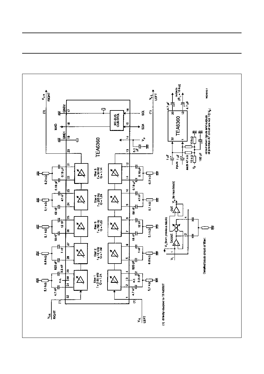
Fig.1 Block diagram, test and application circuit.
May 1991
4
Philips Semiconductors
Preliminary specification
5-band stereo equalizer circuit
TEA6360
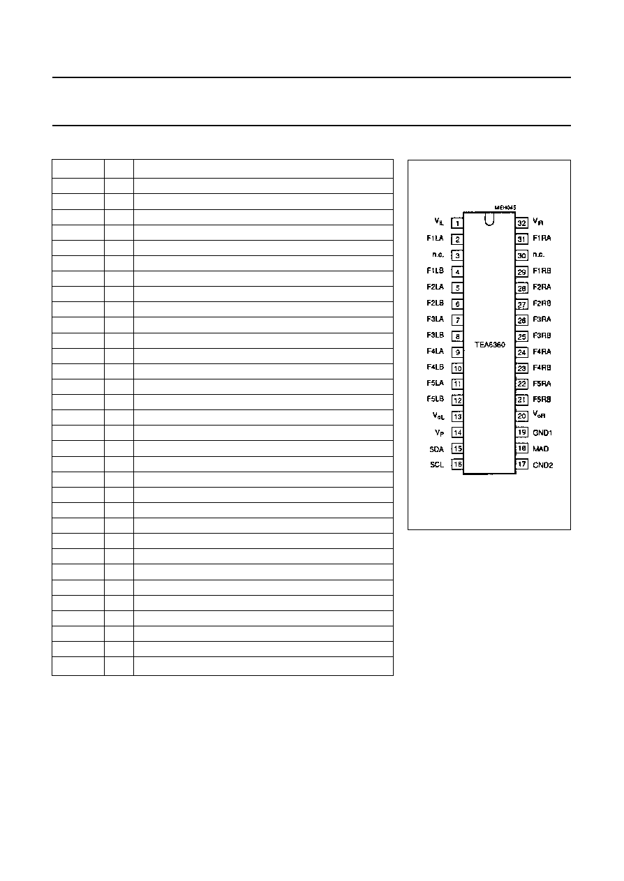
PINNING
SYMBOL
PIN
DESCRIPTION
V
iL
1
audio frequency input LEFT
F1LA
2
connection A for filter 1 LEFT (f = 2.95 kHz)
n.c.
3
not connected
F1LB
4
connection B for filter 1 LEFT (f = 2.95 kHz)
F2LA
5
connection A for filter 2 LEFT (f = 12 kHz)
F2LB
6
connection B for filter 2 LEFT (f = 12 kHz)
F3LA
7
connection A for filter 3 LEFT (f = 790 Hz)
F3LB
8
connection B for filter 3 LEFT (f = 790 Hz)
F4LA
9
connection A for filter 4 LEFT (f = 205 Hz)
F4LB
10
connection B for filter 4 LEFT (f = 205 Hz)
F5LA
11
connection A for filter 5 LEFT (f = 59 Hz)
F5LB
12
connection B for filter 5 LEFT (f = 59 Hz)
V
oL
13
audio frequency output LEFT
V
P
14
supply voltage (
+
8.5 V)
SDA
15
I
2
C-bus data line
SCL
16
I
2
C-bus clock line
GND2
17
ground 2 (I
2
C-bus ground)
MAD
18
modul address
GND1
19
ground 1 (analog ground)
V
oR
20
audio frequency output RIGHT
F5RB
21
connection B for filter 5 RIGHT (f = 59 Hz)
F5RA
22
connection A for filter 5 RIGHT (f = 59 Hz)
F4RB
23
connection B for filter 4 RIGHT (f = 205 Hz)
F4RA
24
connection A for filter 4 RIGHT (f = 205 Hz)
F3RB
25
connection B for filter 3 RIGHT (f = 790 Hz)
F3RA
26
connection A for filter 3 RIGHT (f = 790 Hz)
F2RB
27
connection B for filter 2 RIGHT (f = 12 kHz)
F2RA
28
connection A for filter 2 RIGHT (f = 12 kHz)
F1RB
29
connection B for filter 1 RIGHT (f = 2.95 kHz)
n.c.
30
not connected
F1RA
31
connection A for filter 1 RIGHT (f = 2.95 kHz)
V
iR
32
audio frequency input RIGHT
Fig.2 Pin configuration
May 1991
5
Philips Semiconductors
Preliminary specification
5-band stereo equalizer circuit
TEA6360
FUNCTIONAL DESCRIPTION
The TEA6360 is performed with two stereo channels
(RIGHT and LEFT), each one consists of five equal filter
amplifiers (Fig.1).
The centre frequencies for the different filters as well as
the bandwidth and the control ranges for boost and cut
depend on the external components. Each filter can have
different external components but for one definite pair of
filters the centre frequency as well as the control range for
boost and cut are the same. That means, they have
symmetrical curves for boost and cut.
The control range (maximum value in dB) is divided into
five steps and one extra step for the linear position.
At maximum gain of 12 dB the typical step resolution is
2.4 dB. The internal resistor chain of each filter amplifier is
optimized for 12 dB maximum gain. Therefore the typical
gain factors for 15 dB application are as follows:
The control of the different filters is obtained by selecting
the appropriate subaddress byte (Table 1).
step 1
= 2.7
dB
step 2
= 5.5
dB
step 3
= 8.4
dB
step 4
= 11.6
dB
step 5
= 15.0
dB
The position of the filter in the left channel and that in the
right channel is always the same (stereo).
The position of the boost part and the cut part is
independently controllable (Tables 2 and 3).
The quality factor of the filter has its maximum in the
maximum position (steps 5), if boost (cut on step 0) or cut
(boost on step 0) is used. The quality factor decreases also
with the step number (variable quality factor).
In this mode the control pattern are according to Table 4.
A different control is necessary to achieve a constant
quality factor over the whole control range. For boost with
a constant quality factor over the boost range position
+
5
is selected and boost control is then performed using cut.
This control technique is applied to the cut range with
position
-
5 selected and the boost is varied (Table 5).
The cut part has to follow the boost part in each filter for
economic reasons. So the signal is first amplified and then
attenuated. This has to be taken into account for the
internal level diagram in case of constant quality factor.
This may result in a mode between constant Q and
non-constant Q mode; for example for the position
+
2 it is
not necessary to amplify by step
+
5 and then attenuate by
-
3 step. The combination of step
+
4 and step
-
2 to reach
position
+
2 is a good result (quasi constant quality factor,
Table 6).
LIMITING VALUES
In accordance with the Absolute Maximum System (IEC 134).
Ground pins 19, 28 and 43 connected together.
Note
1. Equivalent to discharging a 200 pF capacitor through a 0
series resistor.
SYMBOL
PARAMETER
MIN.
MAX.
UNIT
V
P
supply voltage (pin 14)
0
13.2
V
V
n
voltage on all pins, grounds excluded
0
V
P
V
P
tot
total power dissipation
0
500
mW
T
stg
storage temperature range
-
40
150
░
C
storage temperature range
-
40
150
░
C
T
amb
operating ambient temperature range
-
40
85
░
C
V
ESD
electrostatic handling
(1)
for all pins
▒
500
V

May 1991
6
Philips Semiconductors
Preliminary specification
5-band stereo equalizer circuit
TEA6360
CHARACTERISTICS
V
P
= 8.5 V; f
i
= 1 kHz (R
S
= 600
), R
L
= 10 k
, T
amb
= 25
░
C and measurements taken in Fig.1, unless otherwise
specified.
SYMBOL
PARAMETER
CONDITIONS
MIN.
TYP.
MAX.
UNIT
V
P
supply voltage. range (pin 14)
7
8.5
13.2
V
I
P
supply current (pin 14)
V
P
= 8.5 V
-
25.5
-
mA
V
P
= 12 V
-
26.0
-
mA
Analog part
R
i
input resistor (pins 1 and 32)
1
-
-
M
V
1,32
input voltage range at any stage
2.1 to
V
P
-
1
-
-
V
V
13,20
output voltage range at any stage
1.0 to
V
P
-
1
-
-
V
V
o
output signal level (RMS value, pins 13
control range 0 to
+
5,
and 20)
variable Q-factor or
quasi constant Q-factor 1.1
-
-
V
R
o
output resistor (pins 13 and 20)
-
100
-
R
L
admissable load resistance at outputs
(pins 13 and 20)
2
-
-
k
C
L
admissable load capacitance at outputs
(pins 13 and 20)
-
-
2.5
nF
G
v
total signal gain (G = V
o
/ V
i
)
all filters linear
-
0.5
-
0
dB
B
frequency response
all filters linear, roll off
frequency for
-
1 dB
minimum value
(DC-coupled)
0
-
-
Hz
maximum value
20
-
-
kHz
Cr
crosstalk attenuation between channels
f = 250 to 10000 Hz
all filters linear
60
75
-
dB
all filters maximum boost
55
-
-
dB
all filters maximum cut
55
-
-
dB
THD
distortion (pins 13 and 20)
f = 20 to 12500 Hz
V
P
= 8.5 to 12 V
V
o (rms)
= 1.1 V
all fIlters linear
-
0.2
0.5
%
V
o (rms)
= 0.1 V
all fIlters linear
-
0.05
0.2
%
V
o (rms)
= 1.1 V
all fIlters max. boost
-
0.5
1.0
%
V
o (rms)
= 0.1 V
all fIlters max. boost
-
0.1
0.3
%
V
o (rms)
= 0.1 V
all fIlters maximum cut
-
0.2
0.5
%
V
o (rms)
= 1 V
all fIlters max. boost
f = 1 kHz
-
-
0.35
%

May 1991
7
Philips Semiconductors
Preliminary specification
5-band stereo equalizer circuit
TEA6360
V
N
weighted output noise voltage
CCIR 468-3, maximum
(RMS value)
gain/filter of 12 dB
defeat mode
-
8
16
Á
V
all filters linear
-
23
46
Á
V
all filters maximum boost
-
70
140
Á
V
all filters maximum cut
-
23
46
Á
V
Cr
crosstalk between bus inputs and signal
outputs, 20 log (V
bus
(p-p)/V
o
rms)
all filters linear
-
120
-
dB
RR
ripple rejection at V
ripple
rms < 200 mV
all filters linear
for f = 100 Hz
-
70
-
dB
for f = 40 to 12500 Hz
-
60
-
dB
Internal filters of analog part
Q
Q-factor dependent on maximum gain
maximum gain 10 dB
0.1
-
1.2
maximum gain 12 dB
0.1
-
1.4
maximum gain 15 dB
0.1
-
1.8
R
tot
total resistor of different filter sections
29.6
37.0
44.4
k
R
tot
tolerance between any filter section
-
-
▒
4
%
Internal controls of analog part via I
2
C-bus
Step
number of steps for boost or for cut
-
5
-
position for linear
-
1
-
step resolution
maximum gain 12 dB
-
2.4
-
dB
step set error
-
0.5
-
dB
V
o
DC offset between any step or
neighbouring step or defeat
-
-
▒
10
mV
I
2
C-bus control SDA and SCL (pins 15 and 16)
V
IH
input level HIGH
3
-
V
P
V
V
lL
input level LOW
0
-
1.5
V
I
I
input current
-
-
▒
10
Á
A
V
ACK
acknowledge voltage on SDA
l
15
= 3 mA at LOW
-
-
0.4
V
Module address bit (pin 18)
V
IH
input level HIGH for address 1000 0110
3
-
V
p
V
V
IL
input level LOW for address 1000 0100
0
-
1.5
V
I
I
input current
-
-
▒
10
Á
A
Power on reset: When reset is active the DEF-bit (defeat) is set and the I
2
C-bus receiver is in reset position.
RESET
start of reset
increasing V
P
-
-
2.5
V
decreasing V
P
4.2
5.0
5.8
V
end of reset
increasing V
P
5.2
6.0
6.8
V
SYMBOL
PARAMETER
CONDITIONS
MIN.
TYP.
MAX.
UNIT

May 1991
8
Philips Semiconductors
Preliminary specification
5-band stereo equalizer circuit
TEA6360
Fig.3
Frequency response for maximum boost of
+
12 dB according to Fig.1.
For maximum cut the curves are symmetrical to negative gain values.
Fig.4 Application for car radio (V
p
< 8.5 V).

May 1991
9
Philips Semiconductors
Preliminary specification
5-band stereo equalizer circuit
TEA6360
I
2
C-BUS PROTOCOL
I
2
C-bus format
If more than 1 byte DATA are transmitted, then auto-increment of the subaddress is performed.
Byte organisation
Table 1 I
2
C-bus transmission
Function of the bits of Table 1:
S
SLAVE ADDRESS
A
SUBADDRESS
A
DATA
P
S
=
start condition
SLAVE ADDRESS
=
1000 0100 when pin 18 is set LOW
or 1000 0110 when pin 18 is set HIGH or open-circuit
A
=
acknowledge, generated by the slave
SUBADDRESS
=
subadress byte, see Table 1
DATA
=
data byte, see Table 1
P
=
stop condition
FUNCTION
SUBADDRESS BYTE
DATA BYTE
D7
D6
D5
D4
D3
D2
D1
D0
filter 1/defeat
0
0
0
0
0
0
0
0
DEF
1B2
1B1
1B0
0
1C2
1C1
1C0
filter 2
0
0
0
0
0
0
0
1
0
2B2
2B1
2B0
0
2C2
2C1
2C0
filter 3
0
0
0
0
0
0
1
0
0
3B2
3B1
3B0
0
3C2
3C1
3C0
filter 4
0
0
0
0
0
0
1
1
0
4B2
4B1
4B0
0
4C2
4C1
4C0
filter 5
0
0
0
0
0
1
0
0
0
5B2
5B1
5B0
0
5C2
5C1
5C0
1B0
to
1B2
boost control for filter 1
1B0
to
1B2
cut control for filter 1
2B0
to
2B2
boost control for filter 2
2B0
to
2B2
cut control for filter 2
3B0
to
3B2
boost control for filter 3
3B0
to
3B2
cut control for filter 3
4B0
to
4B2
boost control for filter 4
4B0
to
4B2
cut control for filter 4
5B0
to
5B2
boost control for filter 5
5B0
to
5B2
cut control for filter 5
DEF
DEF = 0 (defeat bit):
All filters operating.
DEF = 1:
Linear frequency response, input is directly connected to the output of the
output amplifier. The filter settings are stored but the internal amplification
is controlled to 0 dB, independent on bits nB2 to nB0.

May 1991
10
Philips Semiconductors
Preliminary specification
5-band stereo equalizer circuit
TEA6360
Table 2
Boost control for filter n
DATA
POSITION
nB2
nB1
nB0
step 0
(no boost)
0
0
0
step 1
0
0
1
step 2
0
1
0
step 3
0
1
1
step 4
1
0
0
step 5
(maximum boost)
1
0
1
step 5
(maximum boost)
1
1
0
step 5
(maximum boost)
1
1
1
Table 3
Cut control for filter n
DATA
POSITION
nB2
nB1
nB0
step 0
(no cut)
0
0
0
step 1
0
0
1
step 2
0
1
0
step 3
0
1
1
step 4
1
0
0
step 5
(maximum cut)
1
0
1
step 5
(maximum cut)
1
1
0
step 5
(maximum cut)
1
1
1
Table 4
Filter control with variable quality factor
POSITION
D7
D6
D5
D4
D3
D2
D1
D0
COMMENT
X
nB2
nB1
nB0
X
nC2
nC1
nC0
+
5
(maximum boost)
0
1
0
1
0
0
0
0
(
+
5)
+
(
-
0)
=
+
5
+
4
0
1
0
0
0
0
0
0
(
+
4)
+
(
-
0)
=
+
4
+
3
0
0
1
1
0
0
0
0
(
+
3)
+
(
-
0)
=
+
3
+
2
0
0
1
0
0
0
0
0
(
+
2)
+
(
-
0)
=
+
2
+
1
0
0
0
1
0
0
0
0
(
+
1)
+
(
-
0)
=
+
1
0
(linear)
0
0
0
0
0
0
0
0
(
+
0)
+
(
-
0)
=
0
-
1
0
0
0
0
0
0
0
1
(
+
0)
+
(
-
1)
=
-
1
-
2
0
0
0
0
0
0
1
0
(
+
0)
+
(
-
2)
=
-
2
-
3
0
0
0
0
0
0
1
1
(
+
0)
+
(
-
3)
=
-
3
-
4
0
0
0
0
0
1
0
0
(
+
0)
+
(
-
4)
=
-
4
-
5
(maximum cut)
0
0
0
0
0
1
0
1
(
+
0)
+
(
-
5)
=
-
5

May 1991
11
Philips Semiconductors
Preliminary specification
5-band stereo equalizer circuit
TEA6360
Table 5
Filter control with constant quality factor
Table 6
Filter control with quasi-constant quality factor
POSITION
D7
D6
D5
D4
D3
D2
D1
D0
COMMENT
X
nB2
nB1
nB0
X
nC2
nC1
nC0
+
5
(maximum boost)
0
1
0
1
0
0
0
0
(
+
5)
+
(
-
0)
=
+
5
+
4
0
1
0
1
0
0
0
1
(
+
5)
+
(
-
1)
=
+
4
+
3
0
1
0
1
0
0
1
0
(
+
5)
+
(
-
2)
=
+
3
+
2
0
1
0
1
0
0
1
1
(
+
5)
+
(
-
3)
=
+
2
+
1
0
1
0
1
0
1
0
0
(
+
5)
+
(
-
4)
=
+
1
0
(linear)
0
0
0
0
0
0
0
0
(
+
0)
+
(
-
0)
=
0
-
1
0
1
0
0
0
1
0
1
(
+
4)
+
(
-
5)
=
-1
-
2
0
0
1
1
0
1
0
1
(
+
3)
+
(
-
5)
=
-2
-
3
0
0
1
0
0
1
0
1
(
+
2)
+
(
-
5)
=
-
3
-
4
0
0
0
1
0
1
0
1
(
+
1)
+
(
-
5)
=
-
4
-
5
(maximum cut)
0
0
0
0
0
1
0
1
(
+
0)
+
(
-
5)
=
-
5
POSITION
D7
D6
D5
D4
D3
D2
D1
D0
COMMENT
X
nB2
nB1
nB0
X
nC2
nC1
nC0
+
5
(maximum boost)
0
1
0
1
0
0
0
0
(
+
5)
+
(
-
0)
=
+
5
+
4
0
1
0
1
0
0
0
1
(
+
5)
+
(
-
1)
=
+
4
+
3
0
1
0
1
0
0
1
0
(
+
5)
+
(
-
2)
=
+
3
+
2
0
1
0
0
0
0
1
0
(
+
4)
+
(
-
2)
=
+
2
+
1
0
0
1
1
0
0
1
0
(
+
3)
+
(
-
2)
=
+
1
0
(linear)
0
0
0
0
0
0
0
0
(
+
0)
+
(
-
0)
=
0
-
1
0
0
1
0
0
0
1
1
(
+
2)
+
(
-
3)
=
-
1
-
2
0
0
1
0
0
1
0
0
(
+
2)
+
(
-
4)
=
-
2
-
3
0
0
1
0
0
1
0
1
(
+
2)
+
(
-
5)
=
-
3
-
4
0
0
0
1
0
1
0
1
(
+
1)
+
(
-
5)
=
-
4
-
5
(maximum cut)
0
0
0
0
0
1
0
1
(
+
0)
+
(
-
5)
=
-
5

May 1991
12
Philips Semiconductors
Preliminary specification
5-band stereo equalizer circuit
TEA6360
PACKAGE OUTLINES
UNIT
b
1
c
E
e
M
H
L
REFERENCES
OUTLINE
VERSION
EUROPEAN
PROJECTION
ISSUE DATE
IEC
JEDEC
EIAJ
mm
DIMENSIONS (mm are the original dimensions)
SOT232-1
92-11-17
95-02-04
b
max.
w
M
E
e
1
1.3
0.8
0.53
0.40
0.32
0.23
29.4
28.5
9.1
8.7
3.2
2.8
0.18
1.778
10.16
10.7
10.2
12.2
10.5
1.6
4.7
0.51
3.8
M
H
c
(e )
1
M
E
A
L
seating plane
A
1
w
M
b
1
e
D
A
2
Z
32
1
17
16
b
E
pin 1 index
0
5
10 mm
scale
Note
1. Plastic or metal protrusions of 0.25 mm maximum per side are not included.
(1)
(1)
D
(1)
Z
A
max.
1
2
A
min.
A
max.
SDIP32: plastic shrink dual in-line package; 32 leads (400 mil)
SOT232-1
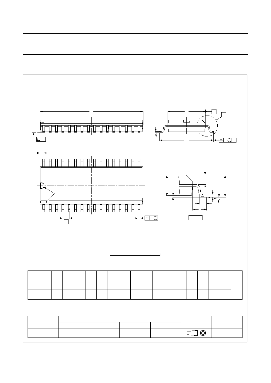
May 1991
13
Philips Semiconductors
Preliminary specification
5-band stereo equalizer circuit
TEA6360
UNIT
A
max.
A
1
A
2
A
3
b
p
c
D
(1)
E
(1)
e
H
E
L
L
p
Q
Z
y
w
v
REFERENCES
OUTLINE
VERSION
EUROPEAN
PROJECTION
ISSUE DATE
IEC
JEDEC
EIAJ
mm
inches
2.65
0.10
0.25
0.01
1.4
0.055
0.3
0.1
2.45
2.25
0.49
0.36
0.27
0.18
20.7
20.3
7.6
7.4
1.27
10.65
10.00
1.2
1.0
0.95
0.55
8
0
o
o
0.25
0.1
0.004
0.25
DIMENSIONS (inch dimensions are derived from the original mm dimensions)
Note
1. Plastic or metal protrusions of 0.15 mm maximum per side are not included.
1.1
0.4
SOT287-1
92-11-17
95-01-25
(1)
0.012
0.004
0.096
0.086
0.02
0.01
0.050
0.047
0.039
0.42
0.39
0.30
0.29
0.81
0.80
0.011
0.007
0.037
0.022
0.01
0.01
0.043
0.016
w
M
b
p
D
H
E
Z
e
c
v
M
A
X
A
y
32
17
16
1
A
A
1
A
2
L
p
Q
detail X
L
(A )
3
E
pin 1 index
0
5
10 mm
scale
SO32: plastic small outline package; 32 leads; body width 7.5 mm
SOT287-1

May 1991
14
Philips Semiconductors
Preliminary specification
5-band stereo equalizer circuit
TEA6360
SOLDERING
Introduction
There is no soldering method that is ideal for all IC
packages. Wave soldering is often preferred when
through-hole and surface mounted components are mixed
on one printed-circuit board. However, wave soldering is
not always suitable for surface mounted ICs, or for
printed-circuits with high population densities. In these
situations reflow soldering is often used.
This text gives a very brief insight to a complex technology.
A more in-depth account of soldering ICs can be found in
our
"IC Package Databook" (order code 9398 652 90011).
SDIP
S
OLDERING BY DIPPING OR BY WAVE
The maximum permissible temperature of the solder is
260
░
C; solder at this temperature must not be in contact
with the joint for more than 5 seconds. The total contact
time of successive solder waves must not exceed
5 seconds.
The device may be mounted up to the seating plane, but
the temperature of the plastic body must not exceed the
specified maximum storage temperature (T
stg max
). If the
printed-circuit board has been pre-heated, forced cooling
may be necessary immediately after soldering to keep the
temperature within the permissible limit.
R
EPAIRING SOLDERED JOINTS
Apply a low voltage soldering iron (less than 24 V) to the
lead(s) of the package, below the seating plane or not
more than 2 mm above it. If the temperature of the
soldering iron bit is less than 300
░
C it may remain in
contact for up to 10 seconds. If the bit temperature is
between 300 and 400
░
C, contact may be up to 5 seconds.
SO
R
EFLOW SOLDERING
Reflow soldering techniques are suitable for all SO
packages.
Reflow soldering requires solder paste (a suspension of
fine solder particles, flux and binding agent) to be applied
to the printed-circuit board by screen printing, stencilling or
pressure-syringe dispensing before package placement.
Several techniques exist for reflowing; for example,
thermal conduction by heated belt. Dwell times vary
between 50 and 300 seconds depending on heating
method. Typical reflow temperatures range from
215 to 250
░
C.
Preheating is necessary to dry the paste and evaporate
the binding agent. Preheating duration: 45 minutes at
45
░
C.
W
AVE SOLDERING
Wave soldering techniques can be used for all SO
packages if the following conditions are observed:
À
A double-wave (a turbulent wave with high upward
pressure followed by a smooth laminar wave) soldering
technique should be used.
À
The longitudinal axis of the package footprint must be
parallel to the solder flow.
À
The package footprint must incorporate solder thieves at
the downstream end.
During placement and before soldering, the package must
be fixed with a droplet of adhesive. The adhesive can be
applied by screen printing, pin transfer or syringe
dispensing. The package can be soldered after the
adhesive is cured.
Maximum permissible solder temperature is 260
░
C, and
maximum duration of package immersion in solder is
10 seconds, if cooled to less than 150
░
C within
6 seconds. Typical dwell time is 4 seconds at 250
░
C.
A mildly-activated flux will eliminate the need for removal
of corrosive residues in most applications.
R
EPAIRING SOLDERED JOINTS
Fix the component by first soldering two diagonally-
opposite end leads. Use only a low voltage soldering iron
(less than 24 V) applied to the flat part of the lead. Contact
time must be limited to 10 seconds at up to 300
░
C. When
using a dedicated tool, all other leads can be soldered in
one operation within 2 to 5 seconds between
270 and 320
░
C.

May 1991
15
Philips Semiconductors
Preliminary specification
5-band stereo equalizer circuit
TEA6360
DEFINITIONS
LIFE SUPPORT APPLICATIONS
These products are not designed for use in life support appliances, devices, or systems where malfunction of these
products can reasonably be expected to result in personal injury. Philips customers using or selling these products for
use in such applications do so at their own risk and agree to fully indemnify Philips for any damages resulting from such
improper use or sale.
PURCHASE OF PHILIPS I
2
C COMPONENTS
Data sheet status
Objective specification
This data sheet contains target or goal specifications for product development.
Preliminary specification
This data sheet contains preliminary data; supplementary data may be published later.
Product specification
This data sheet contains final product specifications.
Limiting values
Limiting values given are in accordance with the Absolute Maximum Rating System (IEC 134). Stress above one or
more of the limiting values may cause permanent damage to the device. These are stress ratings only and operation
of the device at these or at any other conditions above those given in the Characteristics sections of the specification
is not implied. Exposure to limiting values for extended periods may affect device reliability.
Application information
Where application information is given, it is advisory and does not form part of the specification.
Purchase of Philips I
2
C components conveys a license under the Philips' I
2
C patent to use the
components in the I
2
C system provided the system conforms to the I
2
C specification defined by
Philips. This specification can be ordered using the code 9398 393 40011.