Document Outline
- FEATURES
- APPLICATIONS
- GENERAL DESCRIPTION
- ORDERING INFORMATION
- QUICK REFERENCE DATA
- BLOCK DIAGRAM
- PINNING
- LIMITING VALUES
- HANDLING
- THERMAL CHARACTERISTICS
- CHARACTERISTICS
- APPLICATION INFORMATION
- PACKAGE OUTLINE
- SOLDERING
- DATA SHEET STATUS
- DEFINITIONS
- DISCLAIMERS

DATA SHEET
Product specification
Supersedes data of 2000 Oct 12
File under Integrated Circuits, IC02
2000 Nov 14
INTEGRATED CIRCUITS
TDA8787A
10-bit, 3.0 V, up to 25 Msps
analog-to-digital interface for CCD
cameras

2000 Nov 14
2
Philips Semiconductors
Product specification
10-bit, 3.0 V, up to 25 Msps analog-to-digital
interface for CCD cameras
TDA8787A
FEATURES
À
Correlated Double Sampling (CDS), Programmable
Gain Amplifier (PGA), 10-bit Analog-to-Digital Converter
(ADC) and reference regulator included
À
Fully programmable via a 3-wire serial interface
À
Sampling frequency up to 25 MHz;
(TDA8787AHL = 18 MHz; TDA8787AHL/S1 = 25 MHz)
À
PGA gain range of 36 dB (in steps of 0.1 dB)
À
Low power consumption of only 170 mW at 2.7 V
À
Power consumption in standby mode of 4.5 mW
(typical value)
À
3.0 V operation; 2.5 to 3.6 V operation for the digital
outputs
À
Active control pulses polarity selectable via serial
interface
À
8-bit DAC included for analog settings
À
TTL compatible inputs, CMOS compatible outputs.
APPLICATIONS
À
Low-power, low-voltage CCD camera systems.
GENERAL DESCRIPTION
The TDA8787A is a 10-bit analog-to-digital interface for
CCD cameras. The device includes a correlated double
sampling circuit, a PGA, clamp loops and a low-power
10-bit ADC, together with its reference voltage regulator.
The PGA gain and the ADC input clamp level are
controlled via the serial interface.
An additional DAC is provided for additional system
controls. Its output voltage range is 1.0 V peak-to-peak
which is available at pin OFDOUT.
ORDERING INFORMATION
TYPE NUMBER
PACKAGE
NAME
DESCRIPTION
VERSION
PIXEL
FREQUENCY
TDA8787AHL
LQFP48
plastic low profile quad flat package; 48 leads;
body 7
Î
7
Î
1.4 mm
SOT313-2
18 MHz
TDA8787AHL/S1
LQFP48
SOT313-2
25 MHz

2000 Nov 14
3
Philips Semiconductors
Product specification
10-bit, 3.0 V, up to 25 Msps analog-to-digital
interface for CCD cameras
TDA8787A
QUICK REFERENCE DATA
SYMBOL
PARAMETER
CONDITIONS
MIN.
TYP.
MAX.
UNIT
V
CCA
analog supply voltage
2.7
3.0
3.6
V
V
CCD
digital supply voltage
2.7
3.0
3.6
V
V
CCO
digital outputs stages supply
voltage
2.5
2.6
3.6
V
I
CCA
analog supply current
all clamps active; f
pix
= 18 MHz
-
50
60
mA
I
CCD
digital supply current
f
pix
= 18 MHz
-
13
17
mA
I
CCO
digital outputs supply current
f
pix
= 18 MHz; C
L
= 20 pF; input ramp
response time is 800
Á
s
-
1
2
mA
ADC
res
ADC resolution
-
10
-
bits
V
i(CDS)(p-p)
CDS input amplitude (video
signal) (peak-to-peak value)
V
CC
= 2.85 V
650
-
-
mV
V
CC
3.0 V
800
-
-
mV
f
pix(max)
maximum pixel frequency
25
-
-
MHz
f
pix(min)
minimum pixel frequency
2
-
-
MHz
DR
PGA
PGA dynamic range
-
36
-
dB
N
tot(rms)
total noise (RMS value) at
CDS input to ADC output
PGA code = 0; see Fig.8
-
0.15
-
LSB
V
n(i)(eq)(rms)
equivalent input noise
voltage (RMS value)
PGA code = 383
-
70
-
Á
V
P
tot
total power consumption
V
CCA
= V
CCD
= V
CCO
= 3 V
-
190
-
mW
V
CCA
= V
CCD
= V
CCO
= 2.7 V
-
170
-
mW
2000
Nov
14
4
Philips Semiconductors
Product specification
10-bit, 3.0 V
,
up to 25 Msps analog-to-digital
interf
ace f
or CCD camer
as
TD
A8787A
This text is here in white to force landscape pages to be rotated correctly when browsing through the pdf in the Acrobat reader.This text is here in
_
white to force landscape pages to be rotated correctly when browsing through the pdf in the Acrobat reader.This text is here inThis text is here in
white to force landscape pages to be rotated correctly when browsing through the pdf in the Acrobat reader. white to force landscape pages to be ...
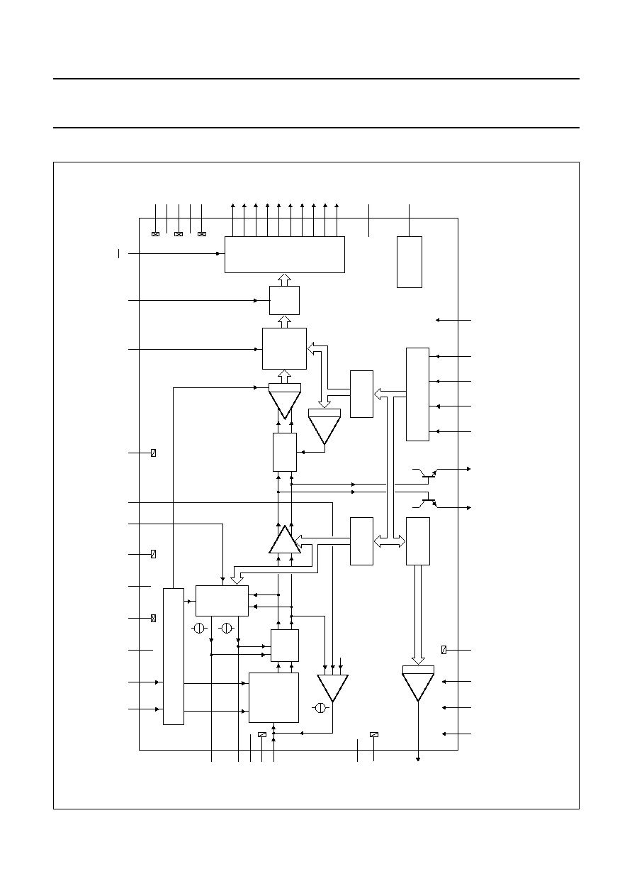
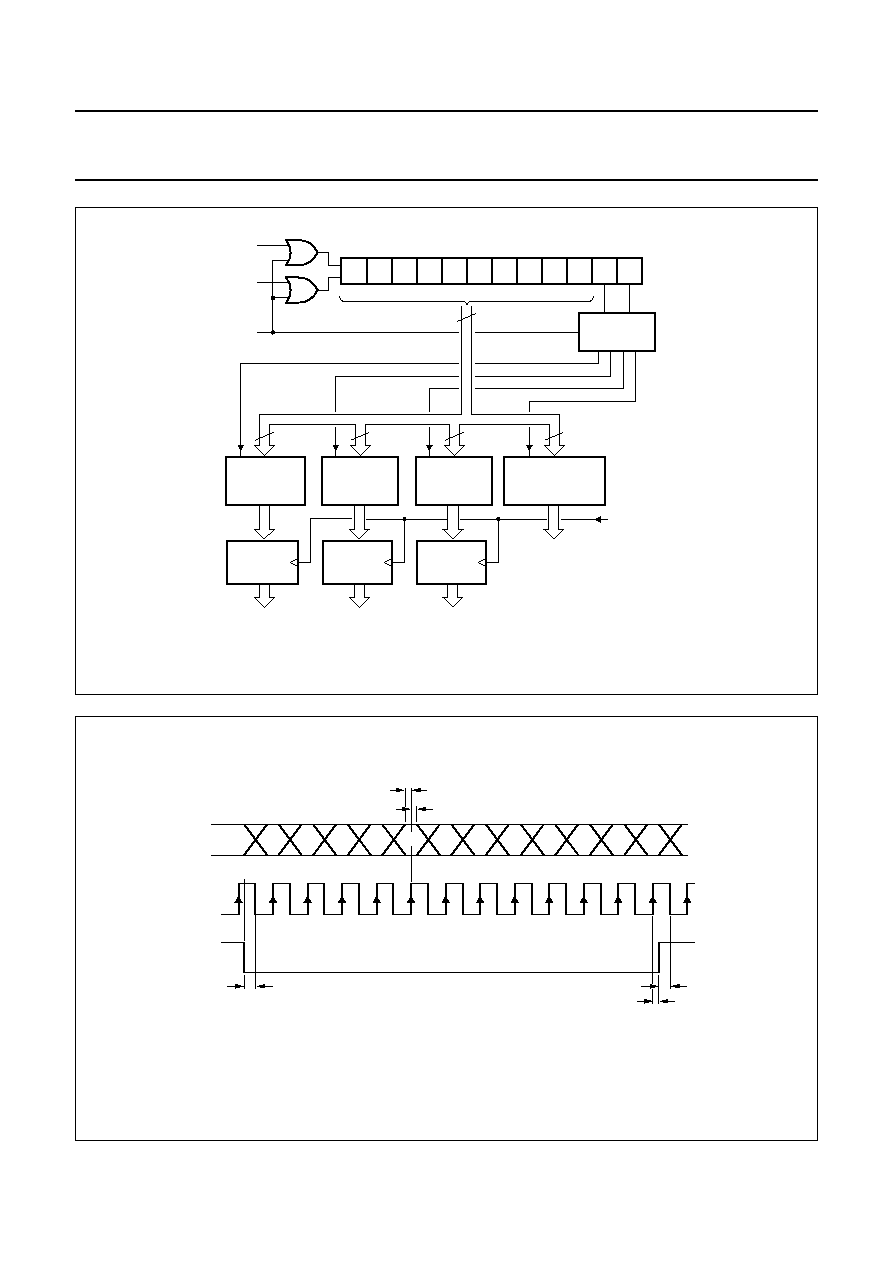
BLOCK DIA
GRAM
d
book, full pagewidth
FCE330
10-bit ADC
REGULATOR
CDS CLOCK GENERATOR
BLANKING
OUTPUT
BUFFER
26
27
28
29
30
31
32
33
34
35
36
37
D9
D8
D7
D6
D5
D4
D3
D2
D1
D0
OGND
25
VCCO
44
DCLPC
38
VCCD2
39
DGND2
19
VCCD1
20
DGND1
41
AGND3
42
VCCA3
8
CPCDS2
7
CPCDS1
4
IN
5
AGND1
9
OFDOUT
6
VCCA1
OE
11
BLK
40
CLK
43
AGND5
17
AGND2
2
DGND3
1
VCCD3
18
VCCA2
12
CLPDM
13
CLPOB
47
SHP
SHIFTER
SHIFT
CORRELATED
DOUBLE
SAMPLING
7-BIT
REGISTER
9-BIT
REGISTER
8-BIT
REGISTER
46
45
OPGA
OPGAC
16
15
14
3
TEST1
AGND4
TEST2
TEST3
48
SHD
SERIAL
INTERFACE
21
22
23
SEN
SCLK SDATA
24
VSYNC
10
STDBY
PGA
DAC
input
clamp
Vref
OFD DAC
LATCH
CLAMP
TDA8787AHL
Fig.1 Block diagram.

2000 Nov 14
5
Philips Semiconductors
Product specification
10-bit, 3.0 V, up to 25 Msps analog-to-digital
interface for CCD cameras
TDA8787A
PINNING
SYMBOL
PIN
DESCRIPTION
V
CCD3
1
digital supply voltage 3
DGND3
2
digital ground 3
AGND4
3
analog ground 4
IN
4
input signal from CCD
AGND1
5
analog ground 1
V
CCA1
6
analog supply voltage 1
CPCDS1
7
clamp storage capacitor 1
CPCDS2
8
clamp storage capacitor 2
OFDOUT
9
analog output of the additional 8-bit control DAC
STDBY
10
standby mode control input (LOW: TDA8787A active; HIGH: TDA8787A standby)
BLK
11
blanking control input
CLPDM
12
clamp pulse input at dummy pixel (should be connected to ground)
CLPOB
13
clamp pulse input for optical black
TEST1
14
test pin input 1 (should be connected to AGND2)
TEST2
15
test pin input 2 (should be connected to AGND2)
TEST3
16
test pin input 3 (should be connected to AGND2)
AGND2
17
analog ground 2
V
CCA2
18
analog supply voltage 2
V
CCD1
19
digital supply voltage 1
DGND1
20
digital ground 1
SDATA
21
serial data input for serial interface control
SCLK
22
serial clock input for serial interface control
SEN
23
strobe pin for serial interface control
VSYNC
24
vertical sync pulse input
V
CCO
25
output stages supply voltage
OGND
26
digital output ground
D0
27
ADC digital output 0 (LSB)
D1
28
ADC digital output 1
D2
29
ADC digital output 2
D3
30
ADC digital output 3
D4
31
ADC digital output 4
D5
32
ADC digital output 5
D6
33
ADC digital output 6
D7
34
ADC digital output 7
D8
35
ADC digital output 8
D9
36
ADC digital output 9 (MSB)
OE
37
output enable control input (LOW: outputs active; HIGH: outputs in high impedance)
V
CCD2
38
digital supply 2
DGND2
39
digital ground 2
CLK
40
data clock input

2000 Nov 14
6
Philips Semiconductors
Product specification
10-bit, 3.0 V, up to 25 Msps analog-to-digital
interface for CCD cameras
TDA8787A
AGND3
41
analog ground 3
V
CCA3
42
analog supply 3
AGND5
43
analog ground 5
DCLPC
44
regulator decoupling pin
OPGA
45
PGA output (test pin)
OPGAC
46
PGA complementary output (test pin)
SHP
47
preset sample-and-hold pulse input
SHD
48
data sample-and-hold pulse input
SYMBOL
PIN
DESCRIPTION
1
2
3
4
5
6
7
8
9
10
11
36
35
34
33
32
31
30
29
28
27
26
13
14
15
16
17
18
19
20
21
22
23
48
47
46
45
44
43
42
41
40
39
38
12
24
37
25
TDA8787AHL
FCE331
D9
D8
D7
D6
D4
D3
D2
D1
D0
OGND
VCCO
VCCD3
DGND3
AGND4
IN
AGND1
VCCA1
CPCDS2
OFDOUT
BLK
CLPDM
D5
SHP
OPGAC
OPGA
DCLPC
AGND5
V
CCA3
CLK
DGND2
OE
V
CCD2
SHD
AGND3
CPCDS1
STDBY
TEST1
TEST2
TEST3
AGND2
V
CCA2
V
CCD1
DGND1
SCLK
SEN
VSYNC
CLPOB
SDATA
Fig.2 Pin configuration.
2000 Nov 14
7
Philips Semiconductors
Product specification
10-bit, 3.0 V, up to 25 Msps analog-to-digital
interface for CCD cameras
TDA8787A
LIMITING VALUES
In accordance with the Absolute Maximum Rating System (IEC 60134).
Note
1. The supply voltages V
CCA
, V
CCD
and V
CCO
may have any value between
-
0.3 and +5.0 V provided that the supply
voltage difference
V
CC
remains as indicated.
HANDLING
Inputs and outputs are protected against electrostatic discharges in normal handling. However, to be totally safe, it is
desirable to take normal precautions appropriate to handling integrated circuits.
THERMAL CHARACTERISTICS
SYMBOL
PARAMETER
CONDITIONS
MIN.
MAX.
UNIT
V
CCA
analog supply voltage
note 1
-
0.3
+5.0
V
V
CCD
digital supply voltage
note 1
-
0.3
+5.0
V
V
CCO
output stages supply voltage
note 1
-
0.3
+5.0
V
V
CC
supply voltage difference
between V
CCA
and V
CCD
-
0.5
+0.5
V
between V
CCA
and V
CCO
-
0.5
+1.2
V
between V
CCD
and V
CCO
-
0.5
+1.2
V
V
i
input voltage
referenced to AGND
-
0.3
+5.0
V
I
o
data output current
-
▒
10
mA
T
stg
storage temperature
-
55
+150
░
C
T
amb
ambient temperature
-
20
+75
░
C
T
j
junction temperature
-
150
░
C
SYMBOL
PARAMETER
CONDITIONS
VALUE
UNIT
R
th(j-a)
thermal resistance from junction to ambient
in free air
76
K/W

2000 Nov 14
8
Philips Semiconductors
Product specification
10-bit, 3.0 V, up to 25 Msps analog-to-digital
interface for CCD cameras
TDA8787A
CHARACTERISTICS
V
CCA
= V
CCD
= 3.0 V; V
CCO
= 2.6 V; f
pix
= 18 MHz; T
amb
=
-
20 to +75
░
C; unless otherwise specified.
SYMBOL
PARAMETER
CONDITIONS
MIN.
TYP.
MAX.
UNIT
Supplies
V
CCA
analog supply voltage
2.7
3.0
3.6
V
V
CCD
digital supply voltage
2.7
3.0
3.6
V
V
CCO
digital outputs stages
supply voltage
2.5
2.6
3.6
V
I
CCA
analog supply current
all clamps active
-
50
60
mA
I
CCD
digital supply current
-
13
17
mA
I
CCO
digital outputs supply
current
C
L
= 20 pF on all data outputs;
input ramp response time is
800
Á
s
-
1
2
mA
P
tot
total power consumption
V
CCA
= V
CCD
= V
CCO
= 3 V
-
190
-
mW
V
CCA
= V
CCD
= V
CCO
= 2.7 V
-
170
-
mW
Digital inputs
I
NPUTS
:
PINS
STDBY, CLPDM, CLPOB, SCLK, SDATA, SEN, VSYNC, OE, CLK
AND
BLK
V
IL
LOW-level input voltage
0
-
0.6
V
V
IH
HIGH-level input voltage
2.2
-
5.0
V
I
i
input current
0
V
i
V
CCD
-
2
-
+2
Á
A
I
NPUTS
:
PINS
SHP
AND
SHD
V
IL
LOW-level input voltage
0
-
0.6
V
V
IH
HIGH-level input voltage
2.2
-
5.0
V
I
i
input current
0
V
i
V
CCD
-
10
-
+10
Á
A
Clamps
G
LOBAL CHARACTERISTICS OF THE CLAMP LOOPS
t
W(clamp)
clamp active pulse width
in numbers of pixels
PGA input code = 255 for
maximum 4 LSB error
12
-
-
pixels
I
NPUT CLAMP
:
PIN
CLPDM
g
m(CDS)
CDS input clamp
transconductance
1.5
2.7
3.5
mS
O
PTICAL BLACK CLAMP
:
PIN
CLPOB
G
shift
gain from CPCDS1 and 2
to PGA inputs
-
0.27
-
I
LSB(cp)
charge pump current for
▒
1 LSB error at ADC
output
PGA input code = 0
-
▒
20
-
Á
A
PGA input code = 383
-
▒
0.60
-
Á
A
2000 Nov 14
9
Philips Semiconductors
Product specification
10-bit, 3.0 V, up to 25 Msps analog-to-digital
interface for CCD cameras
TDA8787A
Correlated Double Sampling (CDS) (pin IN)
V
i(CDS)(p-p)
CDS input amplitude
(video signal)
(peak-to-peak value)
V
CC
= 2.85 V
650
-
-
mV
V
CC
3.0 V
800
-
-
mV
V
i(rst)(max)
maximum CDS input reset
pulse amplitude
500
-
-
mV
I
i
input current
at floating gate level
-
1
-
+1
Á
A
C
i
input capacitance
-
2
-
pF
t
CDS(min)
CDS control pulses
minimum active time
V
i(CDS)(p-p)
= 800 mV;
black-to-white transition in
1 pixel (
▒
2 LSB typical);
T
amb
= 25
░
C; note 1
f
pix
= 18 MHz
(TDA8787AHL)
11
15
-
ns
f
pix
= 25 MHz
(TDA8787AHL/S1)
9
11
-
ns
t
h(IN-SHP)
hold time SHP to IN
T
amb
= 25
░
C; see
Figs 3 and 4
-
1
2
ns
t
h(IN-SHD)
hold time SHD to IN
T
amb
= 25
░
C; see
Figs 3 and 4
-
1
2
ns
Amplifier
DR
PGA
PGA dynamic range
-
36
-
dB
G
PGA
PGA gain step
-
0.3
-
+0.3
dB
Analog-to-Digital Converter (ADC)
LE
(i)
integral non-linearity error
f
pix
= 18 MHz; ramp input
-
▒
1.3
▒
2.5
LSB
LE
(d)
differential non-linearity
error
f
pix
= 18 MHz; ramp input
-
▒
0.5
▒
0.9
LSB
Total chain characteristics (CDS, PGA and ADC)
f
pix(max)
maximum pixel frequency
25
-
-
MHz
f
pix(min)
minimum pixel frequency
2
-
-
MHz
t
CLKH
clock HIGH time
15
-
-
ns
t
CLKL
clock LOW time
15
-
-
ns
t
d(SHD-CLK)
time delay SHD to CLK
see Fig.3
10
-
-
ns
t
su(BLK-CLK)
set-up time of
BLK compared to CLK
10
-
-
ns
V
i(IN)
video input dynamic signal
for ADC full-scale output
PGA input code = 0
800
-
-
mV
PGA input code = 383
12.7
-
-
mV
N
tot(rms)
total noise from CDS input
to ADC output
(RMS value)
see Fig.8
PGA input code = 0
-
0.15
-
LSB
PGA input code = 96
-
0.8
-
LSB
V
n(i)(eq)(rms)
equivalent input noise
voltage (RMS value)
PGA input code = 383
-
70
-
Á
V
PGA input code = 0
-
120
-
Á
V
SYMBOL
PARAMETER
CONDITIONS
MIN.
TYP.
MAX.
UNIT

2000 Nov 14
10
Philips Semiconductors
Product specification
10-bit, 3.0 V, up to 25 Msps analog-to-digital
interface for CCD cameras
TDA8787A
Note
1. Depending on application environments and especially in case of high gain operation and digital supply with jitter, it
is preferable to apply 12 ns or higher CDS pulses.
O
CCD(max)
maximum offset between
CCD floating level and
CCD dark pixel level
-
80
-
+80
mV
Digital-to-Analog Converter (OFDOUT DAC)
V
OFDOUT(p-p)
additional 8-bit control
DAC (OFD) output voltage
(peak-to-peak value)
R
L
= 1 M
-
1.0
-
V
V
OFDOUT
DC output voltage
OFD input code 0
-
AGND
-
V
OFD input code 255
-
AGND + 1.0
-
V
TC
OFD
OFD output range
temperature coefficient
-
250
-
ppm/
░
C
Z
OFDOUT
OFD output impedance
-
2000
-
I
OFDOUT
OFD output drive current
static
-
-
100
Á
A
Digital outputs (f
pix
= 18 MHz; C
L
= 10 pF); see Figs 3 and 4
V
OH
HIGH-level output voltage
I
OH
=
-
1 mA
V
CCO
-
0.5
-
V
CCO
V
V
OL
LOW-level output voltage
I
OL
= 1 mA
0
-
0.5
V
I
OZ
OFF-state output current
0.5 V < V
OZ
< V
CCO
-
20
-
+20
Á
A
t
h(o)
output hold time
9
-
-
ns
t
d(o)
output delay time
V
CCO
= 3.0 V
-
17
23
ns
V
CCO
= 2.7 V
-
19
25
ns
C
L
load capacitance
-
-
22
pF
Serial interface
f
SCLK(max)
maximum frequency
pin SCLK
5
-
-
MHz
SYMBOL
PARAMETER
CONDITIONS
MIN.
TYP.
MAX.
UNIT

2000 Nov 14
11
Philips Semiconductors
Product specification
10-bit, 3.0 V, up to 25 Msps analog-to-digital
interface for CCD cameras
TDA8787A
handbook, full pagewidth
N
0.6 V
0.6 V
2.2 V
N
+
1
N
+
2
N
+
3
tCDS(min)
tCLKH
th(IN-SHP)
0.6 V
0.6 V
0.6 V
0.6 V
0.6 V
th(IN-SHD)
0.6 V
2.2 V
2.2 V
tCDS(min)
td(SHD-CLK)
tsu(BLK-CLK)
2.2 V
FCE337
IN
SHP
SHD
CLK
DATA
BLK
th(o)
td(o)
N
-
1
N
50%
Fig.3 Pixel frequency timing diagram with active HIGH-level polarities.

2000 Nov 14
12
Philips Semiconductors
Product specification
10-bit, 3.0 V, up to 25 Msps analog-to-digital
interface for CCD cameras
TDA8787A
handbook, full pagewidth
N
0.6 V
0.6 V
2.2 V
N
+
1
N
+
2
N
+
3
tCLKL
th(IN-SHP)
2.2 V
2.2 V
2.2 V
2.2 V
th(IN-SHD)
0.6 V
2.2 V
0.6 V
tCDS(min)
tCDS(min)
td(SHD-CLK)
tsu(BLK-CLK)
0.6 V
0.6 V
FCE328
IN
SHP
SHD
CLK
DATA
BLK
th(o)
td(o)
N
-
1
N
50%
Fig.4 Pixel frequency timing diagram with active LOW-level polarities.

2000 Nov 14
13
Philips Semiconductors
Product specification
10-bit, 3.0 V, up to 25 Msps analog-to-digital
interface for CCD cameras
TDA8787A
handbook, full pagewidth
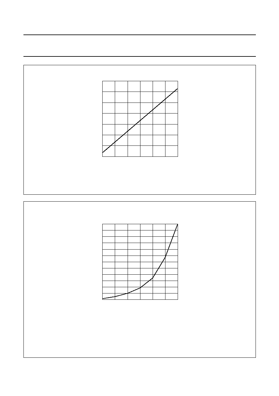
FCE332
0
VOFDOUT
(V)
1.0
0
255
OFD control DAC input code
Fig.5 DAC output voltage output as a function of DAC input code.
handbook, full pagewidth
FCE333
BLK
(active HIGH)
CLPOB
(active HIGH)
PGA output
4 pixels
(1)
VIDEO
OPTICAL BLACK
CLPOB
WINDOW
HORIZONTAL FLYBACK
DUMMY
VIDEO
BLK window
Fig.6 Line frequency timing diagram.
(1) In case the number of clamp pixels is limited to 18
Î
(t
W(clamp)
); otherwise this timing interval can be smaller.
2000 Nov 14
14
Philips Semiconductors
Product specification
10-bit, 3.0 V, up to 25 Msps analog-to-digital
interface for CCD cameras
TDA8787A
0
64
192
320
PGA input code
128
Total
gain
(dB)
256
383
42
30
6
0
12
24
36
18
FCE327
ADC input range is 1 V
pp
.
Fig.7 Total gain as a function of PGA input code.
handbook, halfpage
FCE329
Ntot(rms)
(LSB)
5
4
3
2
0
6
1
0
64
192
320
PGA input code
128
256
383
Noise measurement at ADC outputs; coupling capacitor at input is grounded, so only noise contribution of the front-end is evaluated. Front-end works
at 18 Mpixels with line of 1024 pixels whose first 40 are used to run CLPOB and the last 40 for CLPDM. Data at the ADC outputs are measured during
the other pixels. As a result of this, the standard deviation of the codes statistic is computed, resulting in the noise.
Fig.8 Typical total noise performance as a function of PGA gain.
2000 Nov 14
15
Philips Semiconductors
Product specification
10-bit, 3.0 V, up to 25 Msps analog-to-digital
interface for CCD cameras
TDA8787A
handbook, full pagewidth
OFDOUT DAC
LATCHES
PGA GAIN
LATCHES
ADC CLAMP
LATCHES
CONTROL PULSE
POLARITY
LATCHES
LATCH
SELECTION
SD0
LSB
MSB
SDATA
SCLK
SEN
8-bit DAC
FCE334
PGA
control
ADC clamp
control
control pulses
polarity
settings
VSYNC
SD1 SD2 SD3 SD4 SD5
10
SD6
SHIFT REGISTER
SD7 SD8 SD9
A0
A1
8
9
7
6
FLIP-FLOP
FLIP-FLOP
FLIP-FLOP
Fig.9 Serial interface block diagram.
handbook, full pagewidth
FCE335
SDATA
SCLK
SEN
A1
A0
SD9
SD7
SD6
SD5
SD4
SD3
MSB
LSB
SD2
SD1
SD0
thd3
tsu3
tsu1
thd4
tsu2
SD8
Fig.10 Loading sequence of control input data via the serial interface.
t
su1
= t
su2
= t
su3
= 10 ns (minimum); t
hd3
= t
hd4
= 10 ns (minimum).

2000 Nov 14
16
Philips Semiconductors
Product specification
10-bit, 3.0 V, up to 25 Msps analog-to-digital
interface for CCD cameras
TDA8787A
Table 1
Serial interface programming; see Figs 9 and 10
Table 2
Polarity settings
Note
1. Bit SD4 is not used.
Table 3
Standby mode selection; pin STDBY
Table 4
Output enable (OE) pin 37
ADDRESS BITS
DATA BITS SD9 TO SD0
A1
A0
0
0
PGA gain control (bits SD8 to SD0); bit SD9 should be set to logic 0
0
1
DAC OFDOUT output control (bits SD7 to SD0); bits SD8 and SD9 should be set to
logic 0
1
0
ADC clamp reference control (SD6 to SD0); from code 0 to 127; bits SD7, SD8 and
SD9 should be set to logic 0
1
1
control pulses polarity settings (pins SHP, SHD, CLPDM, CLPOB, BLK and CLK)
SYMBOL
PIN
SERIAL CONTROL BIT
(1)
ACTIVE EDGE OR LEVEL
SHP and SHD
47 and 48
SD0
1 = HIGH; 0 = LOW
CLK
40
SD1
1 = HIGH; 0 = LOW
CLPDM
12 (connected to ground)
SD2
always 0 = LOW
CLPOB
13
SD3
1 = HIGH; 0 = LOW
BLK
11
SD5
1 = HIGH; 0 = LOW
VSYNC
24
SD6
0 = rising; 1 = falling
STDBY
ADC DIGITAL OUTPUTS; PINS D9 TO D0
I
CCA
+ I
CCO
+ I
CCD
(typical)
1
logic state LOW
1.5 mA
0
active
64 mA
OE
ADC DIGITAL OUTPUTS; PINS D9 TO D0
0
active, binary
1
high impedance

2000 Nov 14
17
Philips Semiconductors
Product specification
10-bit, 3.0 V, up to 25 Msps analog-to-digital
interface for CCD cameras
TDA8787A
APPLICATION INFORMATION
Power and grounding recommendations
When designing a printed-circuit board for applications
such as PC cameras, surveillance cameras, camcorders
and digital still cameras, care should be taken to minimize
the noise.
For the front-end integrated circuit, the basic rules
of printed-circuit board design and implementation
of analog components (such as additional operational
amplifiers) must be respected, particularly with respect
to power and ground connections.
The following additional recommendation is given for the
CDS input pin(s) which is /are internally connected to the
programmable gain amplifier.
The connections between the CCD interface and
CDS input should be as short as possible and a ground
ring protection around these connections can be
beneficial. Separate analog and digital supplies provide
the best solution. If this is not possible to do this on the
board then the analog supply pins must be decoupled
effectively from the digital supply pins. If the same power
supply and ground are used for all the pins then the
decoupling capacitors must be placed as close as possible
to the IC package.
In order to minimize the noise due to package and die
parasitics in a two-ground system, the following measures
must be implemented:
À
All the analog and digital supply pins must be decoupled
to the analog ground plane. Only the ground pin
associated with the digital outputs must be connected to
the digital ground plane. All the other ground pins should
be connected to the analog ground plane. The analog
and digital ground planes must be connected together at
one point as close as possible to the ground pin
associated with the digital outputs.
À
The digital output pins and their associated lines should
be shielded by the digital ground plane which can then
be used as a return path for digital signals.
2000 Nov 14
18
Philips Semiconductors
Product specification
10-bit, 3.0 V, up to 25 Msps analog-to-digital
interface for CCD cameras
TDA8787A
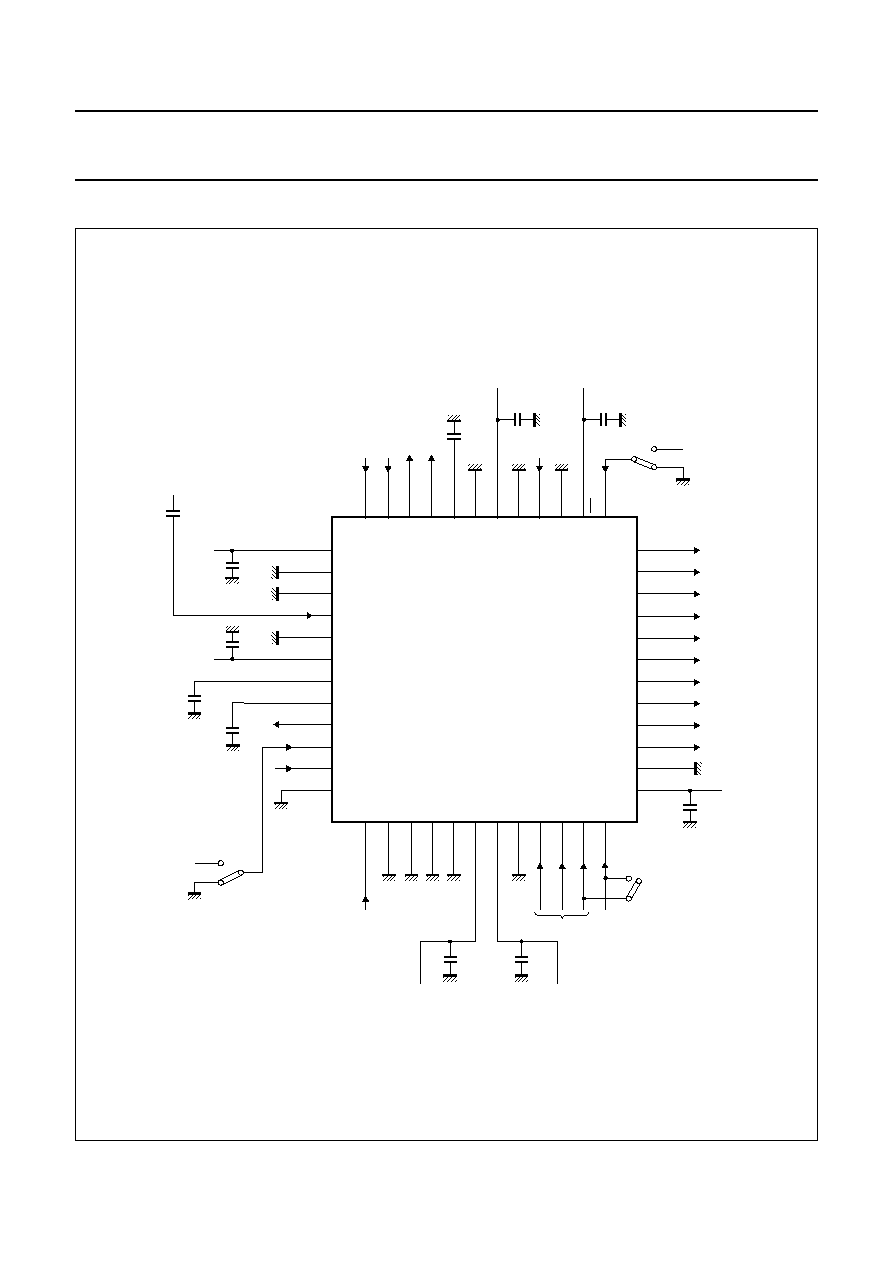
Application diagram
handbook, full pagewidth
FCE336
1
2
3
4
5
6
7
8
9
10
11
36
48
(2)
(2)
47
46
45
44
43
42
41
40
39
38
37
13
14
15
16
17
18
19
20
21
22
23
24
35
34
33
32
31
30
29
28
27
26
12
25
TDA8787AHL
D9
D8
D7
D6
D4
D3
D2
D1
D0
OGND
VCCO
VCCD3
DGND3
AGND4
IN
AGND1
VCCA1
CPCDS2
OFDOUT
BLK
CLPDM
D5
SHP
OPGAC
OPGA
DCLPC
AGND5
V
CCA3
CLK
DGND2
OE
V
CCD2
SHD
AGND3
CPCDS1
STDBY
TEST1
TEST2
TEST3
AGND2
V
CCA2
V
CCD1
DGND1
SCLK
SEN
VSYNC
CLPOB
SDATA
serial interface
VCCA
VCCD
CCD
(2)
VCCD
VCCD
VCCD
VCCA
100 nF
VCCD
100 nF
VCCD
100
nF
100
nF
100
nF
VCCA
100
nF
1
Á
F
1
Á
F
1
Á
F
1
Á
F
1
Á
F
(1)
Fig.11 Application diagram.
(1) Pins SEN and VSYNC should be interconnected when no vertical synchronization signal is available, while control pin VSYNC should be
programmed by serial interface as LOW-level active.
(2) The timing of the signals on pins IN, SHD and SHP has to comply with the hold times t
h(IN-SHP)
and t
h(IN-SHD)
(see Fig.3).

2000 Nov 14
19
Philips Semiconductors
Product specification
10-bit, 3.0 V, up to 25 Msps analog-to-digital
interface for CCD cameras
TDA8787A
PACKAGE OUTLINE
UNIT
A
max.
A
1
A
2
A
3
b
p
c
E
(1)
e
H
E
L
L
p
Z
y
w
v
REFERENCES
OUTLINE
VERSION
EUROPEAN
PROJECTION
ISSUE DATE
IEC
JEDEC
EIAJ
mm
1.60
0.20
0.05
1.45
1.35
0.25
0.27
0.17
0.18
0.12
7.1
6.9
0.5
9.15
8.85
0.95
0.55
7
0
o
o
0.12
0.1
0.2
1.0
DIMENSIONS (mm are the original dimensions)
Note
1. Plastic or metal protrusions of 0.25 mm maximum per side are not included.
0.75
0.45
SOT313-2
MS-026
136E05
99-12-27
00-01-19
D
(1)
(1)
(1)
7.1
6.9
H
D
9.15
8.85
E
Z
0.95
0.55
D
b
p
e
E
B
12
D
H
b
p
E
H
v
M
B
D
ZD
A
Z E
e
v
M
A
1
48
37
36
25
24
13
A
1
A
L
p
detail X
L
(A )
3
A
2
X
y
c
w
M
w
M
0
2.5
5 mm
scale
pin 1 index
LQFP48: plastic low profile quad flat package; 48 leads; body 7 x 7 x 1.4 mm
SOT313-2

2000 Nov 14
20
Philips Semiconductors
Product specification
10-bit, 3.0 V, up to 25 Msps analog-to-digital
interface for CCD cameras
TDA8787A
SOLDERING
Introduction to soldering surface mount packages
This text gives a very brief insight to a complex technology.
A more in-depth account of soldering ICs can be found in
our
"Data Handbook IC26; Integrated Circuit Packages"
(document order number 9398 652 90011).
There is no soldering method that is ideal for all surface
mount IC packages. Wave soldering is not always suitable
for surface mount ICs, or for printed-circuit boards with
high population densities. In these situations reflow
soldering is often used.
Reflow soldering
Reflow soldering requires solder paste (a suspension of
fine solder particles, flux and binding agent) to be applied
to the printed-circuit board by screen printing, stencilling or
pressure-syringe dispensing before package placement.
Several methods exist for reflowing; for example,
infrared/convection heating in a conveyor type oven.
Throughput times (preheating, soldering and cooling) vary
between 100 and 200 seconds depending on heating
method.
Typical reflow peak temperatures range from
215 to 250
░
C. The top-surface temperature of the
packages should preferable be kept below 230
░
C.
Wave soldering
Conventional single wave soldering is not recommended
for surface mount devices (SMDs) or printed-circuit boards
with a high component density, as solder bridging and
non-wetting can present major problems.
To overcome these problems the double-wave soldering
method was specifically developed.
If wave soldering is used the following conditions must be
observed for optimal results:
À
Use a double-wave soldering method comprising a
turbulent wave with high upward pressure followed by a
smooth laminar wave.
À
For packages with leads on two sides and a pitch (e):
¡ larger than or equal to 1.27 mm, the footprint
longitudinal axis is preferred to be parallel to the
transport direction of the printed-circuit board;
¡ smaller than 1.27 mm, the footprint longitudinal axis
must be parallel to the transport direction of the
printed-circuit board.
The footprint must incorporate solder thieves at the
downstream end.
À
For packages with leads on four sides, the footprint must
be placed at a 45
░
angle to the transport direction of the
printed-circuit board. The footprint must incorporate
solder thieves downstream and at the side corners.
During placement and before soldering, the package must
be fixed with a droplet of adhesive. The adhesive can be
applied by screen printing, pin transfer or syringe
dispensing. The package can be soldered after the
adhesive is cured.
Typical dwell time is 4 seconds at 250
░
C.
A mildly-activated flux will eliminate the need for removal
of corrosive residues in most applications.
Manual soldering
Fix the component by first soldering two
diagonally-opposite end leads. Use a low voltage (24 V or
less) soldering iron applied to the flat part of the lead.
Contact time must be limited to 10 seconds at up to
300
░
C.
When using a dedicated tool, all other leads can be
soldered in one operation within 2 to 5 seconds between
270 and 320
░
C.

2000 Nov 14
21
Philips Semiconductors
Product specification
10-bit, 3.0 V, up to 25 Msps analog-to-digital
interface for CCD cameras
TDA8787A
Suitability of surface mount IC packages for wave and reflow soldering methods
Notes
1. All surface mount (SMD) packages are moisture sensitive. Depending upon the moisture content, the maximum
temperature (with respect to time) and body size of the package, there is a risk that internal or external package
cracks may occur due to vaporization of the moisture in them (the so called popcorn effect). For details, refer to the
Drypack information in the
"Data Handbook IC26; Integrated Circuit Packages; Section: Packing Methods".
2. These packages are not suitable for wave soldering as a solder joint between the printed-circuit board and heatsink
(at bottom version) can not be achieved, and as solder may stick to the heatsink (on top version).
3. If wave soldering is considered, then the package must be placed at a 45
░
angle to the solder wave direction.
The package footprint must incorporate solder thieves downstream and at the side corners.
4. Wave soldering is only suitable for LQFP, TQFP and QFP packages with a pitch (e) equal to or larger than 0.8 mm;
it is definitely not suitable for packages with a pitch (e) equal to or smaller than 0.65 mm.
5. Wave soldering is only suitable for SSOP and TSSOP packages with a pitch (e) equal to or larger than 0.65 mm; it is
definitely not suitable for packages with a pitch (e) equal to or smaller than 0.5 mm.
PACKAGE
SOLDERING METHOD
WAVE
REFLOW
(1)
BGA, SQFP
not suitable
suitable
HLQFP, HSQFP, HSOP, HTSSOP, SMS
not suitable
(2)
suitable
PLCC
(3)
, SO, SOJ
suitable
suitable
LQFP, QFP, TQFP
not recommended
(3)(4)
suitable
SSOP, TSSOP, VSO
not recommended
(5)
suitable

2000 Nov 14
22
Philips Semiconductors
Product specification
10-bit, 3.0 V, up to 25 Msps analog-to-digital
interface for CCD cameras
TDA8787A
DATA SHEET STATUS
Note
1. Please consult the most recently issued data sheet before initiating or completing a design.
DATA SHEET STATUS
PRODUCT
STATUS
DEFINITIONS
(1)
Objective specification
Development
This data sheet contains the design target or goal specifications for
product development. Specification may change in any manner without
notice.
Preliminary specification
Qualification
This data sheet contains preliminary data, and supplementary data will be
published at a later date. Philips Semiconductors reserves the right to
make changes at any time without notice in order to improve design and
supply the best possible product.
Product specification
Production
This data sheet contains final specifications. Philips Semiconductors
reserves the right to make changes at any time without notice in order to
improve design and supply the best possible product.
DEFINITIONS
Short-form specification
The data in a short-form
specification is extracted from a full data sheet with the
same type number and title. For detailed information see
the relevant data sheet or data handbook.
Limiting values definition
Limiting values given are in
accordance with the Absolute Maximum Rating System
(IEC 60134). Stress above one or more of the limiting
values may cause permanent damage to the device.
These are stress ratings only and operation of the device
at these or at any other conditions above those given in the
Characteristics sections of the specification is not implied.
Exposure to limiting values for extended periods may
affect device reliability.
Application information
Applications that are
described herein for any of these products are for
illustrative purposes only. Philips Semiconductors make
no representation or warranty that such applications will be
suitable for the specified use without further testing or
modification.
DISCLAIMERS
Life support applications
These products are not
designed for use in life support appliances, devices, or
systems where malfunction of these products can
reasonably be expected to result in personal injury. Philips
Semiconductors customers using or selling these products
for use in such applications do so at their own risk and
agree to fully indemnify Philips Semiconductors for any
damages resulting from such application.
Right to make changes
Philips Semiconductors
reserves the right to make changes, without notice, in the
products, including circuits, standard cells, and/or
software, described or contained herein in order to
improve design and/or performance. Philips
Semiconductors assumes no responsibility or liability for
the use of any of these products, conveys no licence or title
under any patent, copyright, or mask work right to these
products, and makes no representations or warranties that
these products are free from patent, copyright, or mask
work right infringement, unless otherwise specified.

2000 Nov 14
23
Philips Semiconductors
Product specification
10-bit, 3.0 V, up to 25 Msps analog-to-digital
interface for CCD cameras
TDA8787A
NOTES

® Philips Electronics N.V.
SCA
All rights are reserved. Reproduction in whole or in part is prohibited without the prior written consent of the copyright owner.
The information presented in this document does not form part of any quotation or contract, is believed to be accurate and reliable and may be changed
without notice. No liability will be accepted by the publisher for any consequence of its use. Publication thereof does not convey nor imply any license
under patent- or other industrial or intellectual property rights.
Internet: http://www.semiconductors.philips.com
2000
70
Philips Semiconductors ¡ a worldwide company
For all other countries apply to: Philips Semiconductors,
Marketing Communications, Building BE-p, P.O. Box 218, 5600 MD EINDHOVEN,
The Netherlands, Fax. +31 40 27 24825
Argentina: see South America
Australia: 3 Figtree Drive, HOMEBUSH, NSW 2140,
Tel. +61 2 9704 8141, Fax. +61 2 9704 8139
Austria: Computerstr. 6, A-1101 WIEN, P.O. Box 213,
Tel. +43 1 60 101 1248, Fax. +43 1 60 101 1210
Belarus: Hotel Minsk Business Center, Bld. 3, r. 1211, Volodarski Str. 6,
220050 MINSK, Tel. +375 172 20 0733, Fax. +375 172 20 0773
Belgium: see The Netherlands
Brazil: see South America
Bulgaria: Philips Bulgaria Ltd., Energoproject, 15th floor,
51 James Bourchier Blvd., 1407 SOFIA,
Tel. +359 2 68 9211, Fax. +359 2 68 9102
Canada: PHILIPS SEMICONDUCTORS/COMPONENTS,
Tel. +1 800 234 7381, Fax. +1 800 943 0087
China/Hong Kong: 501 Hong Kong Industrial Technology Centre,
72 Tat Chee Avenue, Kowloon Tong, HONG KONG,
Tel. +852 2319 7888, Fax. +852 2319 7700
Colombia: see South America
Czech Republic: see Austria
Denmark: Sydhavnsgade 23, 1780 COPENHAGEN V,
Tel. +45 33 29 3333, Fax. +45 33 29 3905
Finland: Sinikalliontie 3, FIN-02630 ESPOO,
Tel. +358 9 615 800, Fax. +358 9 6158 0920
France: 51 Rue Carnot, BP317, 92156 SURESNES Cedex,
Tel. +33 1 4099 6161, Fax. +33 1 4099 6427
Germany: Hammerbrookstra▀e 69, D-20097 HAMBURG,
Tel. +49 40 2353 60, Fax. +49 40 2353 6300
Hungary: see Austria
India: Philips INDIA Ltd, Band Box Building, 2nd floor,
254-D, Dr. Annie Besant Road, Worli, MUMBAI 400 025,
Tel. +91 22 493 8541, Fax. +91 22 493 0966
Indonesia: PT Philips Development Corporation, Semiconductors Division,
Gedung Philips, Jl. Buncit Raya Kav.99-100, JAKARTA 12510,
Tel. +62 21 794 0040 ext. 2501, Fax. +62 21 794 0080
Ireland: Newstead, Clonskeagh, DUBLIN 14,
Tel. +353 1 7640 000, Fax. +353 1 7640 200
Israel: RAPAC Electronics, 7 Kehilat Saloniki St, PO Box 18053,
TEL AVIV 61180, Tel. +972 3 645 0444, Fax. +972 3 649 1007
Italy: PHILIPS SEMICONDUCTORS, Via Casati, 23 - 20052 MONZA (MI),
Tel. +39 039 203 6838, Fax +39 039 203 6800
Japan: Philips Bldg 13-37, Kohnan 2-chome, Minato-ku,
TOKYO 108-8507, Tel. +81 3 3740 5130, Fax. +81 3 3740 5057
Korea: Philips House, 260-199 Itaewon-dong, Yongsan-ku, SEOUL,
Tel. +82 2 709 1412, Fax. +82 2 709 1415
Malaysia: No. 76 Jalan Universiti, 46200 PETALING JAYA, SELANGOR,
Tel. +60 3 750 5214, Fax. +60 3 757 4880
Mexico: 5900 Gateway East, Suite 200, EL PASO, TEXAS 79905,
Tel. +9-5 800 234 7381, Fax +9-5 800 943 0087
Middle East: see Italy
Netherlands: Postbus 90050, 5600 PB EINDHOVEN, Bldg. VB,
Tel. +31 40 27 82785, Fax. +31 40 27 88399
New Zealand: 2 Wagener Place, C.P.O. Box 1041, AUCKLAND,
Tel. +64 9 849 4160, Fax. +64 9 849 7811
Norway: Box 1, Manglerud 0612, OSLO,
Tel. +47 22 74 8000, Fax. +47 22 74 8341
Pakistan: see Singapore
Philippines: Philips Semiconductors Philippines Inc.,
106 Valero St. Salcedo Village, P.O. Box 2108 MCC, MAKATI,
Metro MANILA, Tel. +63 2 816 6380, Fax. +63 2 817 3474
Poland: Al.Jerozolimskie 195 B, 02-222 WARSAW,
Tel. +48 22 5710 000, Fax. +48 22 5710 001
Portugal: see Spain
Romania: see Italy
Russia: Philips Russia, Ul. Usatcheva 35A, 119048 MOSCOW,
Tel. +7 095 755 6918, Fax. +7 095 755 6919
Singapore: Lorong 1, Toa Payoh, SINGAPORE 319762,
Tel. +65 350 2538, Fax. +65 251 6500
Slovakia: see Austria
Slovenia: see Italy
South Africa: S.A. PHILIPS Pty Ltd., 195-215 Main Road Martindale,
2092 JOHANNESBURG, P.O. Box 58088 Newville 2114,
Tel. +27 11 471 5401, Fax. +27 11 471 5398
South America: Al. Vicente Pinzon, 173, 6th floor,
04547-130 S├O PAULO, SP, Brazil,
Tel. +55 11 821 2333, Fax. +55 11 821 2382
Spain: Balmes 22, 08007 BARCELONA,
Tel. +34 93 301 6312, Fax. +34 93 301 4107
Sweden: Kottbygatan 7, Akalla, S-16485 STOCKHOLM,
Tel. +46 8 5985 2000, Fax. +46 8 5985 2745
Switzerland: Allmendstrasse 140, CH-8027 Z▄RICH,
Tel. +41 1 488 2741 Fax. +41 1 488 3263
Taiwan: Philips Semiconductors, 5F, No. 96, Chien Kuo N. Rd., Sec. 1,
TAIPEI, Taiwan Tel. +886 2 2134 2451, Fax. +886 2 2134 2874
Thailand: PHILIPS ELECTRONICS (THAILAND) Ltd.,
60/14 MOO 11, Bangna Trad Road KM. 3, Bagna, BANGKOK 10260,
Tel. +66 2 361 7910, Fax. +66 2 398 3447
Turkey: Yukari Dudullu, Org. San. Blg., 2.Cad. Nr. 28 81260 Umraniye,
ISTANBUL, Tel. +90 216 522 1500, Fax. +90 216 522 1813
Ukraine: PHILIPS UKRAINE, 4 Patrice Lumumba str., Building B, Floor 7,
252042 KIEV, Tel. +380 44 264 2776, Fax. +380 44 268 0461
United Kingdom: Philips Semiconductors Ltd., 276 Bath Road, Hayes,
MIDDLESEX UB3 5BX, Tel. +44 208 730 5000, Fax. +44 208 754 8421
United States: 811 East Arques Avenue, SUNNYVALE, CA 94088-3409,
Tel. +1 800 234 7381, Fax. +1 800 943 0087
Uruguay: see South America
Vietnam: see Singapore
Yugoslavia: PHILIPS, Trg N. Pasica 5/v, 11000 BEOGRAD,
Tel. +381 11 3341 299, Fax.+381 11 3342 553
Printed in The Netherlands
753504/03/pp
24
Date of release:
2000 Nov 14
Document order number:
9397 750 07755