Philips Semiconductors RF Communications Products
Product specification
SA620
Low voltage LNA, mixer and VCO -- 1GHz
2
December 15, 1993
853-1725 11658
DESCRIPTION
The SA620 is a combined RF amplifier, VCO
with tracking bandpass filter and mixer
designed for high-performance low-power
communication systems from 800-1200MHz.
The low-noise preamplifier has a 1.6dB noise
figure at 900MHz with 11.5dB gain and an
IP3 intercept of -3dBm at the input. The gain
is stabilized by on-chip compensation to vary
less than
±
0.2dB over -40 to +85
°
C
temperature range. The wide-dynamic-range
mixer has an 9dB noise figure and IP3 of
6dBm at the input at 900MHz. An external
LO can be used in place of the internal VCO
for improved mixer input IP3 and a 3mA
reduction in current. The chip incorporates a
through-mode option so the RF amplifier can
be disabled and replaced by an attenuator
(S
21
= 7.5dB). This is useful for improving
the overall dynamic range of the receiver
when in an overload situation. The nominal
current drawn from a single 3V supply is
10.4mA and 7.2mA in the thru-mode.
Additionally, the VCO and Mixer can be
powered down to further reduce the supply
current to 1.2mA.
FEATURES
·
Low current consumption: 10.4mA nominal,
7.2mA with thru-mode activated
·
Outstanding noise figure: 1.6dB for the
amplifier and 9dB for the mixer at 900MHz
·
Excellent gain stability versus temperature
and supply voltage
·
Switchable overload capability
·
Independent LNA, mixer and VCO power
down capability
·
Internal VCO automatic leveling loop
·
Monotonic VCO frequency vs control
voltage
APPLICATIONS
·
900MHz cellular front-end
·
900MHz cordless front-end
·
Spread spectrum receivers
·
RF data links
·
UHF frequency conversion
·
Portable radio
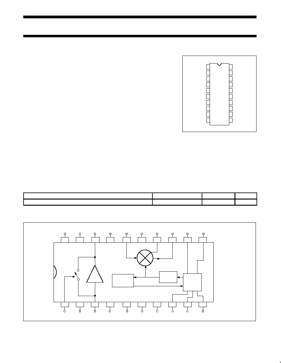
PIN CONFIGURATION
DK Package
1
2
3
4
5
6
7
8
9
10
11
12
13
14
20
19
18
17
16
15
VCC
LNA GND
LNA OUT
LNA BIAS
MIXER IN
MIXER GND
MIXER BYPASS
MIXER OUT
OSC GND
VCO OUT
LNA ENABLE
LNA GND
LNA IN
LNA GND
LNA GND
OSC GND
MIXER PWRDN
OSC PWRDN
OSC1
OSC2
ORDERING INFORMATION
DESCRIPTION
TEMPERATURE RANGE
ORDER CODE
DWG #
20-Pin Plastic Shrink Small Outline Package (Surface-mount, SSOP)
-40 to +85
°
C
SA620DK
1563
BLOCK DIAGRAM
4
3
2
1
5
20
19
18
17
16
7
6
10
9
8
15
14
13
12
11
MIXER
OSC
PWRDN
OSC1
OSC2
VCC
LNA
LNA
BIAS
MIXER
IN
MIXER
GND
MIXER
OUT
OSC
GND
VCO
OUT
LNA
LO
VCO
RF
IF
LNA
ENABLE
LNA
GND
LNA IN
LNA
OSC
GND
AUTOMATIC
LEVELING
LOOP
TRACKING
BANDPASS
FILTER
GND
LNA
OUT
GND
LNA
GND
PWRDN
MIXER
BYPASS
Philips Semiconductors RF Communications Products
Product specification
SA620
Low voltage LNA, mixer and VCO -- 1GHz
December 15, 1993
3
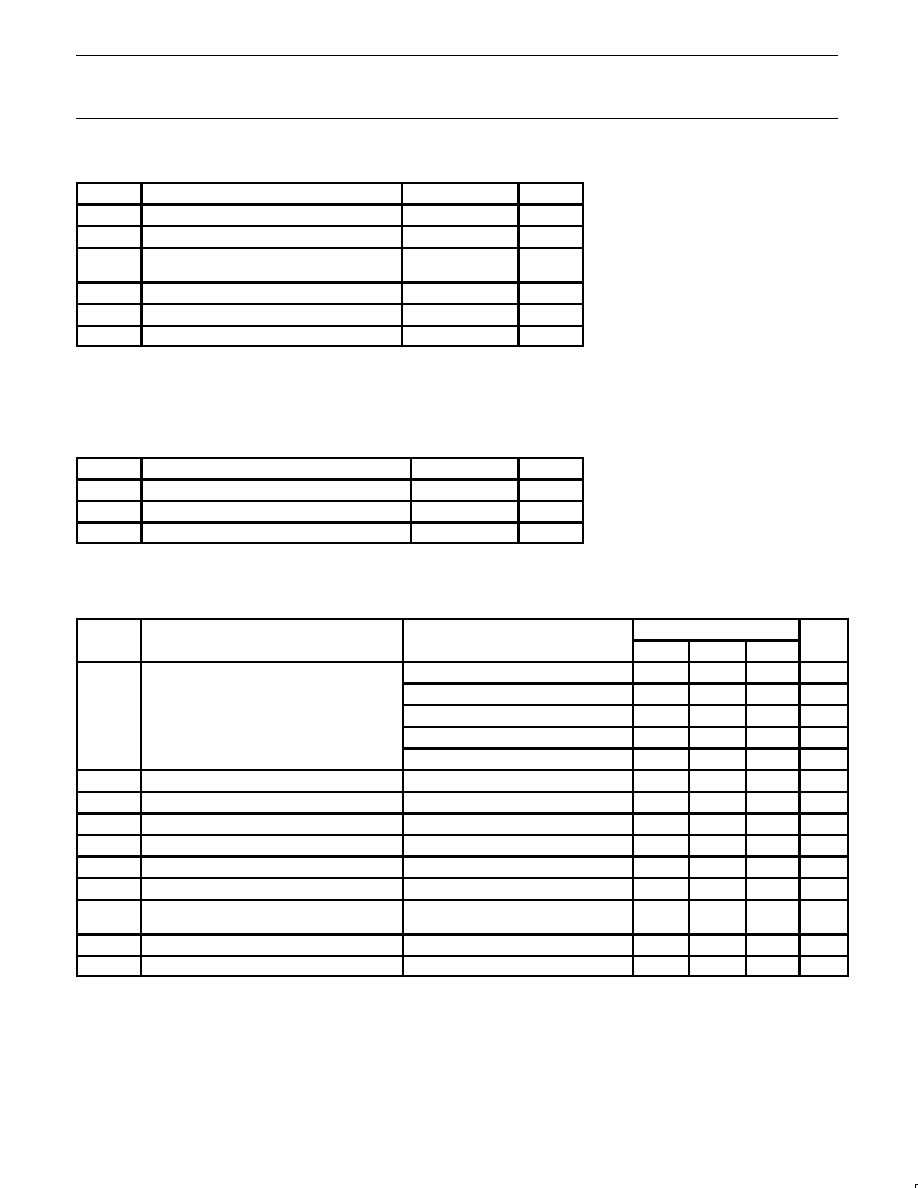
ABSOLUTE MAXIMUM RATINGS
SYMBOL
PARAMETER
RATING
UNITS
V
CC
Supply voltage
1
-0.3 to +6
V
V
IN
Voltage applied to any other pin
-0.3 to (V
CC
+ 0.3)
V
P
D
Power dissipation, T
A
= 25
°
C (still air)
2
20-Pin Plastic SSOP
980
mW
T
JMAX
Maximum operating junction temperature
150
°
C
P
MAX
Maximum power input/output
+20
dBm
T
STG
Storage temperature range
65 to +150
°
C
NOTE:
1. Transients exceeding 8V on V
CC
pin may damage product.
2. Maximum dissipation is determined by the operating ambient temperature and the thermal resistance,
JA
: 20-Pin SSOP
= 110
°
C/W
RECOMMENDED OPERATING CONDITIONS
SYMBOL
PARAMETER
RATING
UNITS
V
CC
Supply voltage
2.7 to 5.5
V
T
A
Operating ambient temperature range
-40 to +85
°
C
T
J
Operating junction temperature
-40 to +105
°
C
DC ELECTRICAL CHARACTERISTICS
V
CC
= +3V, T
A
= 25
°
C; unless otherwise stated.
SYMBOL
PARAMETER
TEST CONDITIONS
LIMITS
UNITS
MIN
TYP
MAX
LNA enable input high
10.4
mA
LNA enable input low
7.2
mA
I
CC
Supply current
VCO power-down input low
7.4
mA
Mixer power-down input low
7.4
mA
Full chip power-down
1.2
mA
V
T
Enable logic threshold voltage
NO TAG
1.2
1.5
1.8
V
V
IH
Logic 1 level
RF amp on
2.0
V
CC
V
V
IL
Logic 0 level
RF amp off
0.3
0.8
V
I
IL
Enable input current
Enable = 0.4V
-1
0
1
µ
A
I
IH
Enable input current
Enable = 2.4V
-1
0
1
µ
A
V
LNAIN
LNA input bias voltage
Enable = 2.4V
0.78
V
V
LNAOU
T
LNA output bias voltage
Enable = 2.4V
2.1
V
V
B
LNA bias voltage
Enable = 2.4V
2.1
V
V
MXIN
Mixer RF input bias voltage
0.94
V
NOTE:
1. The ENABLE input must be connected to a valid logic level for proper operation of the SA620 LNA.
Philips Semiconductors RF Communications Products
Product specification
SA620
Low voltage LNA, mixer and VCO -- 1GHz
December 15, 1993
4
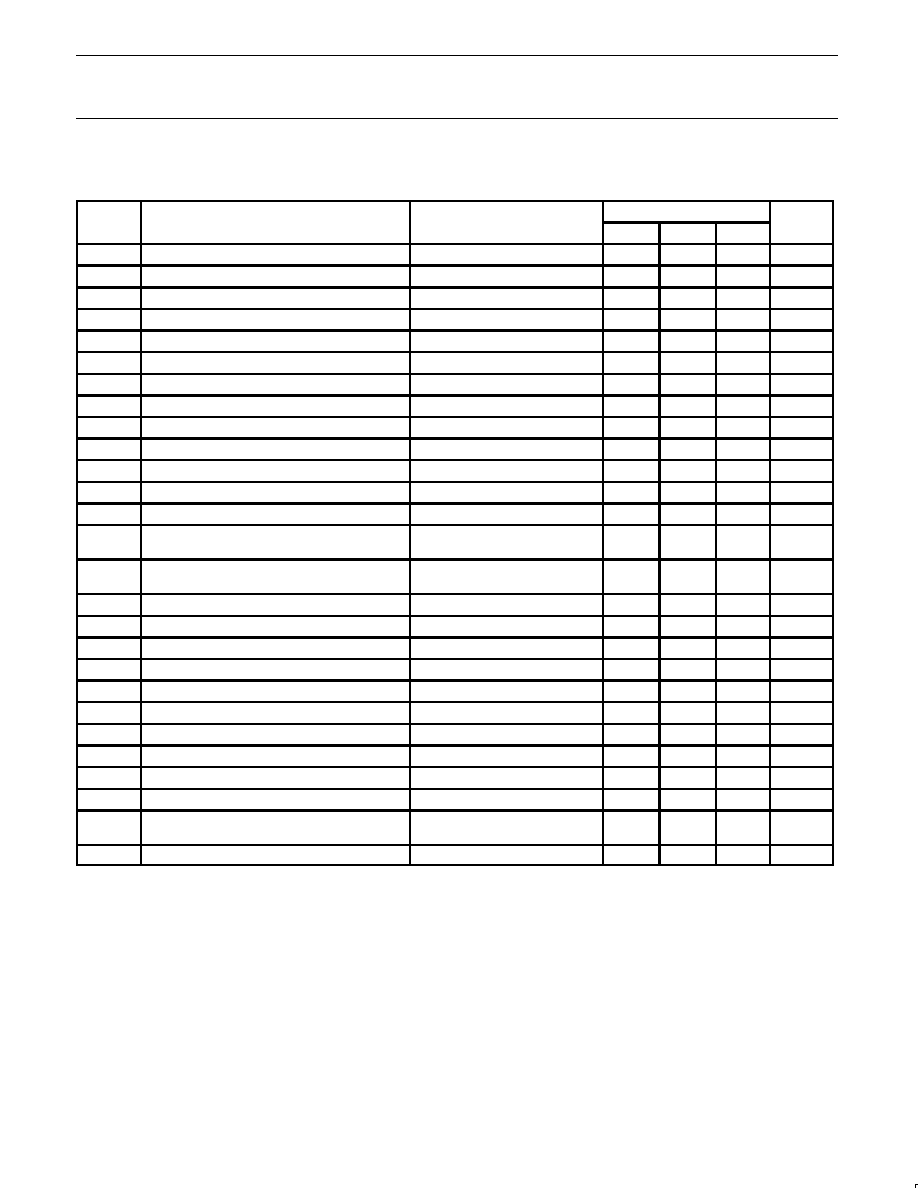
AC ELECTRICAL CHARACTERISTICS
V
CC
= +3V, T
A
= 25
°
C; Enable = +3V; unless otherwise stated.
SYMBOL
PARAMETER
TEST CONDITIONS
LIMITS
UNITS
-3
TYP
+3
S
21
Amplifier gain
900MHz
10
11.5
13
dB
S
21
Amplifier gain in through mode
Enable = 0.4V, 900MHz
-9
-7.5
-6
dB
S
21
/
T
Gain temperature sensitivity in pwr-dwn mode
900MHz
-0.014
dB/
°
C
S
21
/
T
Gain temperature sensitivity enabled
900MHz
0.003
dB/
°
C
S
21
/
f
Gain frequency variation
800MHz - 1.2GHz
0.01
dB/MHz
S
12
Amplifier reverse isolation
900MHz
-20
dB
S
11
Amplifier input match
1
900MHz
-10
dB
S
22
Amplifier output match
1
900MHz
-12
dB
P
-1dB
Amplifier input 1dB gain compression
900MHz
-16
dBm
IP3
Amplifier input third order intercept
900MHz
-4.5
-3
-1.5
dBm
NF
Amplifier noise figure
900MHz
1.3
1.6
1.9
dB
t
ON
Amplifier turn-on time (Enable Lo
Hi)
See Figure 1
50
µ
s
t
OFF
Amplifier turn-off time (Enable Hi
Lo)
See Figure 1
5
µ
s
VG
C
Mixer voltage conversion gain: R
P
= R
L
= 1k
,
f
S
= 0.9GHz, f
LO
= 0.8GHz,
f
IF
= 100MHz
14.5
16
17.5
dB
PG
C
Mixer power conversion gain: R
P
= R
L
= 1k
,
f
S
= 0.9GHz, f
LO
= 0.8GHz,
f
IF
= 100MHz
1.5
3
4.5
dB
S
11M
Mixer input match
1
900MHz
-10
dB
NF
M
Mixer SSB noise figure
900MHz
7.5
9
10.5
dB
P
-1dB
Mixer input 1dB gain compression
900MHz
-13
dBm
IP3
M
Mixer input third order intercept
f
2
f
1
= 1MHz, 900MHz
-7.5
-6
-4.5
dBm
IP
2INT
Mixer input second order intercept
900MHz
12
dBm
P
RFM-IF
Mixer RF feedthrough
900MHz
-20
dB
P
LO-IF
LO feedthrough to IF
900MHz
-25
dBm
P
LO-RFM
LO to mixer input feedthrough
900MHz
-30
dBm
P
LO-RF
LO to LNA input feedthrough
900MHz
-45
dBm
P
VCO
VCO buffer out
900MHz
-16
dBm
VCO frequency range
300
(min)
1200
(max)
MHz
VCO phase noise
Offset = 60kHz
-105
dBc/Hz
NOTE:
1. Simple L/C elements are needed to achieve specified return loss.
Philips Semiconductors RF Communications Products
Product specification
SA620
Low voltage LNA, mixer and VCO -- 1GHz
December 15, 1993
5
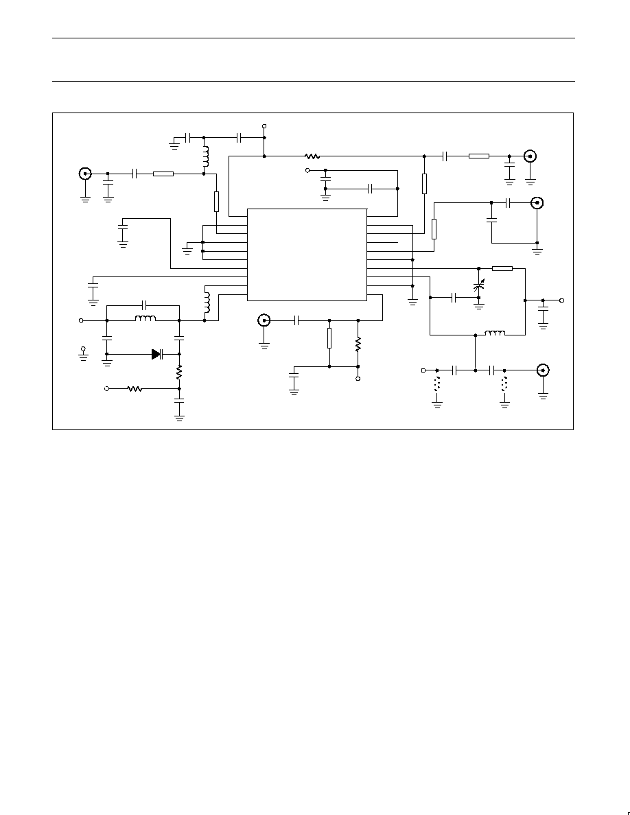
Figure 1. A Complete LNA, Mixer and VCO
1
2
3
4
5
6
7
8
9
10
20
19
18
17
16
15
14
13
12
11
LNA ENABLE
LNA GND
LNA IN
LNA GND
LNA GND
MIXER PD
OSC PD
OSC1
OSC2
Vcc
LNA GND
LNA OUT
LNA BIAS
MIXER IN
MIXER GND
MIXER BYPASS
MIXER OUT
OSC GND
OSC GND
VCO OUT
LNA IN
C1
C23
C22
L1
56nH
C2
1.8pF
C3
C4
C6
L3
2.7nH
C7
3.3pF
D1
SMV 1204 - 099
Alpha Industries
R2
R1
C8
GND
100pF
R6
C19
100pF
C18
2.2pF
LNA OUT
C17
100pF
MIXER IN
C16
5.6pF
C14
1-5pF
R = 9k x (VCC 1)
VCC
C20
100pF
C21
C13
12pF
L4
150nH
C15
R5
C12
10pF
MIXER OUT
L = 260 mils
w = 15 mils
VCO OUT
C9
100pF
R3
C10
100pF
VCC
1
µ
F
0.44
µ
F/(VCC1)
0.1
µ
F
0.1
µ
F
10
µ
F
100pF
0.1
µ
F
0.1
µ
F
(50
)
V_CONTROL
(0 to VCC)
VCC
SA620
VCC
LNA ENABLE
51
(1k
, 83MHz)
10k
22
10k
L = 260 mils
w = 15 mils
L2
2.7nH
C5
3.9pF
4.7nH
535 mils
4.7nH
535 mils
4.7nH
535 mils
4.7nH
535 mils
L = 160 mils
w = 15 mils
C11
1000pF
R4
1k
MIXER OUT
(50
, 83MHz)
CIRCUIT TECHNOLOGY
LNA
Impedance Match: Intrinsic return loss at the
input and output ports is 7dB and 9dB,
respectively. With no external matching, the
associated LNA gain is
10dB and the noise
figure is
1.4dB. However, the return loss
can be improved at 900MHz using suggested
L/C elements (Figure NO TAG) as the LNA is
unconditionally stable.
Noise Match: The LNA achieves 1.6dB
noise figure at 900MHz when S
11
= -10dB.
Further improvements in S
11
will slightly
increase the NF and S
21
.
Thru-Mode: A series switch can be activated
to feed RF signals from LNA input to output
with an attenuator (S
21
= 7.5dB). As a
result, the power handling is greatly improved
and current consumption is decreased by
3.2mA as well. However, if this mode is not
required, C23 and R6 can be deleted.
Temperature Compensation: The LNA has
a built-in temperature compensation scheme
to reduce the gain drift to 0.003dB/
°
C from
40
°
C to +85
°
C.
Supply Voltage Compensation: Unique
circuitry provides gain stabilization over wide
supply voltage range. The gain changes no
more than 0.5dB when V
CC
increases from
3V to 5V.
Mixer
Input Match: The mixer is configured for
maximum gain and best noise figure. The
user needs to supply L/C elements to
achieve this performance.
Mixer Bypass: To optimize the IP3 of the
mixer input, one must adjust the value of C14
for the given board layout. The value
typically lies between 1 and 5pF. Once a
value if selected, a fixed capacitor can be
used. Further improvements in mixer IP3 can
be achieved by inserting a resistive loss at
the mixer input, at the expense of system
gain and noise figure.
Tracking Bandpass Filter: At the LO input
port of the mixer there is a second-order
bandpass filter (approx. 50MHz bandwidth)
which will track the VCO center frequency.
The result is the elimination of low frequency
noise injected into the mixer LO port without
the need for an external LO filter.
Power Down: The mixer can be disabled by
connecting Pin 7 to ground. If a Schottky
diode is connected between Pin 1 (cathode)
and Pin 7 (anode), the LNA disable signal will
control both LNA and mixer simultaneously
When the mixer is disabled, 3mA is saved.
Test Port: Resistor R5 can be substituted
with an external test port of 50
input
impedance. Since R5 and MIXER OUT have
the same output power, the result is a direct
power gain measurement.
VCO
Automatic Leveling Loop: An on-chip
detector and loop amplifier will adjust VCO
bias current to regulate the VCO amplitude
regardless of the Q-factor (>10) of the
resonator and varactor diode. However, the
real current reduction will not occur until the
VCO frequency falls below 500MHz. For a
typical resonator the steady-state current is
3mA at 800MHz.
Buffered VCO Output: The VCO OUT (Pin
11) signal can drive an external prescaler
directly (see also the Philips SA7025 low
voltage, fractional-N synthesizer). The
extracted signal levels need to be limited to
16dBm or less to maintain mixer IIP3.
Phase Noise: If close-in phase noise is not
critical, or if an external synthesizer is used,
C4 (Pin 8) can be decreased to a lower
value.
Power-Down: The VCO can be disabled by
connecting Pin 8 to ground. If a Schottky
diode is connected between Pin 1 (cathode)
and Pin 8 (anode), the LNA disable signal will
control both LNA and VCO simultaneously.
When the VCO is disabled, 3mA is saved.
Philips Semiconductors RF Communications Products
Product specification
SA620
Low voltage LNA, mixer and VCO -- 1GHz
December 15, 1993
6
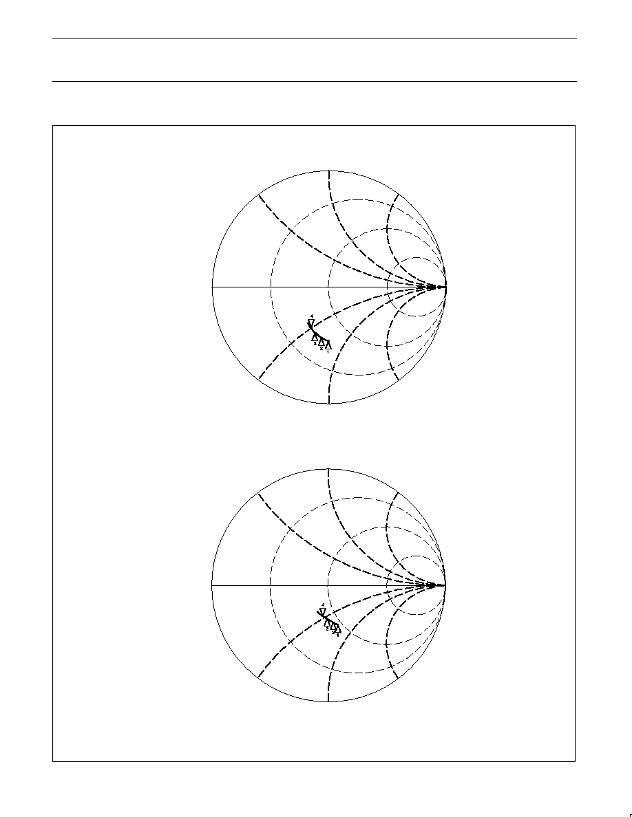
TYPICAL PERFORMANCE CHARACTERISTICS
CH1
S11
1
U
FS
4:
30.707
-24.89
5.86 pF
1100.000 000 MHz
START
800.000 000 MHz
STOP
1200.000 000 MHz
1:
2:
3:
33.184
-39.105
800 MHz
31.879
-33.66
900 MHz
30.594
-28.695
1 GHz
CH1
S22
1
U
FS
4:
39.811
-22.93
6.31 pF
START
800.000 000 MHz
STOP
1200.000 000 MHz
1:
2:
3:
48.164
-35.754
800 MHz
44.574
-31.246
900 MHz
42.068
-25.799
1 GHz
1100.000 000 MHz
Figure 2. LNA Input and Output Match (at Device Pin)