
1.
Product profile
1.1 General description
PESD1LIN in very small SOD323 (SC-76) SMD plastic package designed to protect one
automotive LIN bus line from the damage caused by ElectroStatic Discharge (ESD) and
other transients.
1.2 Features
s
ESD protection of one automotive LIN bus line
s
Asymmetrical diode configuration ensures an optimized Electromagnetical Immunity of
a LIN Electronic Control Unit (ECU)
s
Due to the integrated diode structure only one very small SOD323 package is needed
s
Max. peak pulse power: P
PP
= 160 W at t
p
= 8/20
�
s
s
Low clamping voltage: V
(CL)R
= 40 V at I
PP
= 1 A
s
Ultra low leakage current: I
RM
< 1 nA
s
ESD protection of up to 23 kV
s
IEC 61000-4-2, level 4 (ESD)
s
IEC 61000-4-5 (surge); I
PP
= 3 A at t
p
= 8/20
�
s
1.3 Applications
s
LIN bus protection
s
Automotive applications
1.4 Quick reference data
PESD1LIN
LIN bus ESD protection diode in SOD323
Rev. 01 -- 26 October 2004
Product data sheet
Table 1:
Quick reference data
Symbol
Parameter
Conditions
Min
Typ
Max
Unit
V
RWM
reverse stand-off voltage
PESD1LIN (15 V)
-
-
15
V
PESD1LIN (24 V)
-
-
24
V
C
d
diode capacitance
V
R
= 0 V;
f = 1 MHz
-
13
17
pF

9397 750 14032
� Koninklijke Philips Electronics N.V. 2004. All rights reserved.
Product data sheet
Rev. 01 -- 26 October 2004
2 of 12
Philips Semiconductors
PESD1LIN
LIN bus ESD protection diode in SOD323
2.
Pinning information
3.
Ordering information
4.
Marking
5.
Limiting values
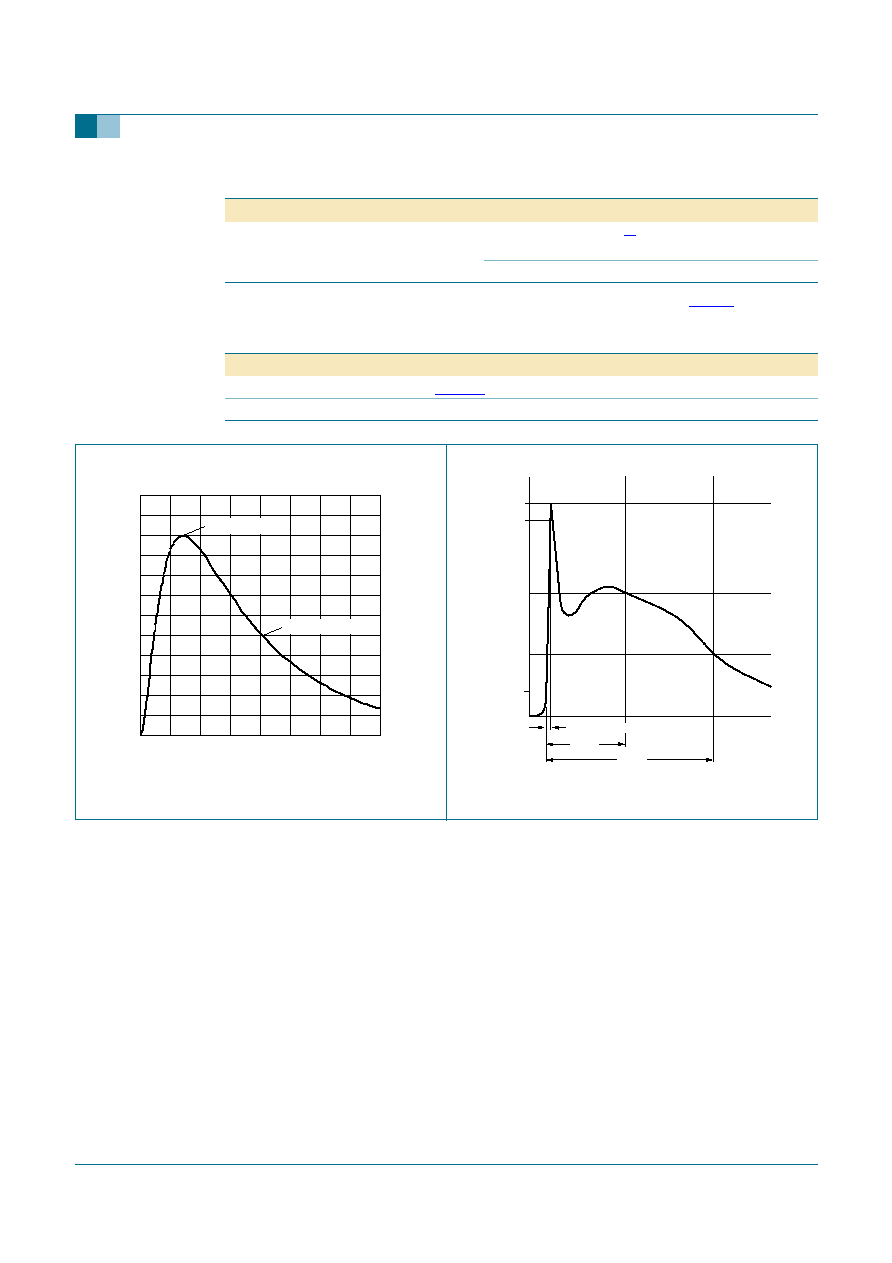
[1]
Non-repetitive current pulse 8/20
�
s exponentially decaying waveform; see
Figure 1
.
Table 2:
Pinning
Pin
Description
Simplified outline
Symbol
1
cathode 1 (15 V)
2
cathode 2 (24 V)
2
1
sym045
2
1
Table 3:
Ordering information
Type number
Package
Name
Description
Version
PESD1LIN
SC-76
plastic surface mounted package; 2 leads
SOD323
Table 4:
Marking codes
Type number
Marking code
PESD1LIN
AM
Table 5:
Limiting values
In accordance with the Absolute Maximum Rating System (IEC 60134).
Symbol
Parameter
Conditions
Min
Max
Unit
P
PP
peak pulse power
8/20
�
s
[1]
-
160
W
I
PP
peak pulse current
8/20
�
s
[1]
-
3
A
T
j
junction temperature
-
150
�
C
T
amb
ambient temperature
-
65
+150
�
C
T
stg
storage temperature
-
65
+150
�
C
9397 750 14032
� Koninklijke Philips Electronics N.V. 2004. All rights reserved.
Product data sheet
Rev. 01 -- 26 October 2004
3 of 12
Philips Semiconductors
PESD1LIN
LIN bus ESD protection diode in SOD323
[1]
Device stressed with ten non-repetitive ElectroStatic Discharge (ESD) pulses; see
Figure 2
.
Table 6:
ESD maximum ratings
Symbol
Parameter
Conditions
Min
Max
Unit
ESD
electrostatic discharge
capability
IEC 61000-4-2
(contact discharge)
[1]
-
23
kV
HBM MIL-STD883
-
10
kV
Table 7:
ESD standards compliance
ESD Standard
Conditions
IEC 61000-4-2, level 4 (ESD); see
Figure 2
> 15 kV (air); > 8 kV (contact)
HBM MIL-STD883, class 3
> 4 kV
Fig 1.
8/20
�
s pulse waveform according to
IEC 61000-4-5.
Fig 2.
ElectroStatic Discharge (ESD) pulse waveform
according to IEC 61000-4-2.
t (
�
s)
0
40
30
10
20
001aaa630
40
80
120
I
pp
(%)
0
e
-
t
100 % I
pp
; 8
�
s
50 % I
pp
; 20
�
s
001aaa631
I
pp
100 %
90 %
t
30 ns
60 ns
10 %
t
r
=
0.7 to 1 ns

9397 750 14032
� Koninklijke Philips Electronics N.V. 2004. All rights reserved.
Product data sheet
Rev. 01 -- 26 October 2004
4 of 12
Philips Semiconductors
PESD1LIN
LIN bus ESD protection diode in SOD323
6.
Characteristics
[1]
Non-repetitive current pulse 8/20
�
s exponentially decaying waveform; see
Figure 1
.
Table 8:
Characteristics
T
amb
= 25
�
C unless otherwise specified.
Symbol
Parameter
Conditions
Min
Typ
Max
Unit
V
RWM
reverse stand-off voltage
PESD1LIN (15 V)
-
-
15
V
PESD1LIN (24 V)
-
-
24
V
I
RM
reverse leakage current
PESD1LIN (15 V)
V
RWM
= 15 V
-
< 1
50
nA
PESD1LIN (24 V)
V
RWM
= 24 V
-
< 1
50
nA
V
(BR)
breakdown voltage
I
R
= 5 mA
PESD1LIN (15 V)
17.1
18.9
20.3
V
PESD1LIN (24 V)
25.4
27.8
30.3
V
C
d
diode capacitance
V
R
= 0 V; f = 1 MHz
-
13
17
pF
V
(CL)R
clamping voltage
[1]
PESD1LIN (15 V)
I
PP
= 1 A
-
-
25
V
I
PP
= 5 A
-
-
44
V
PESD1LIN (24 V)
I
PP
= 1 A
-
-
40
V
I
PP
= 3 A
-
-
70
V
r
dif
differential resistance
PESD1LIN (15 V)
I
R
= 1 mA
-
-
225
PESD1LIN (24 V)
I
R
= 1 mA
-
-
300
9397 750 14032
� Koninklijke Philips Electronics N.V. 2004. All rights reserved.
Product data sheet
Rev. 01 -- 26 October 2004
5 of 12
Philips Semiconductors
PESD1LIN
LIN bus ESD protection diode in SOD323
T
amb
= 25
�
C.
t
p
= 8/20
�
s exponentially decaying waveform; see
Figure 1
.
Fig 3.
Peak pulse power dissipation as a function of
pulse time; typical values.
Fig 4.
Relative variation of peak pulse power as a
function of junction temperature; typical
values.
006aaa164
10
3
10
2
10
4
P
PP
(W)
10
t
p
(
�
s)
1
10
4
10
3
10
10
2
T
j
(
�
C)
0
200
150
50
100
001aaa193
0.4
0.8
1.2
P
pp
0
P
pp(25�C)
9397 750 14032
� Koninklijke Philips Electronics N.V. 2004. All rights reserved.
Product data sheet
Rev. 01 -- 26 October 2004
6 of 12
Philips Semiconductors
PESD1LIN
LIN bus ESD protection diode in SOD323
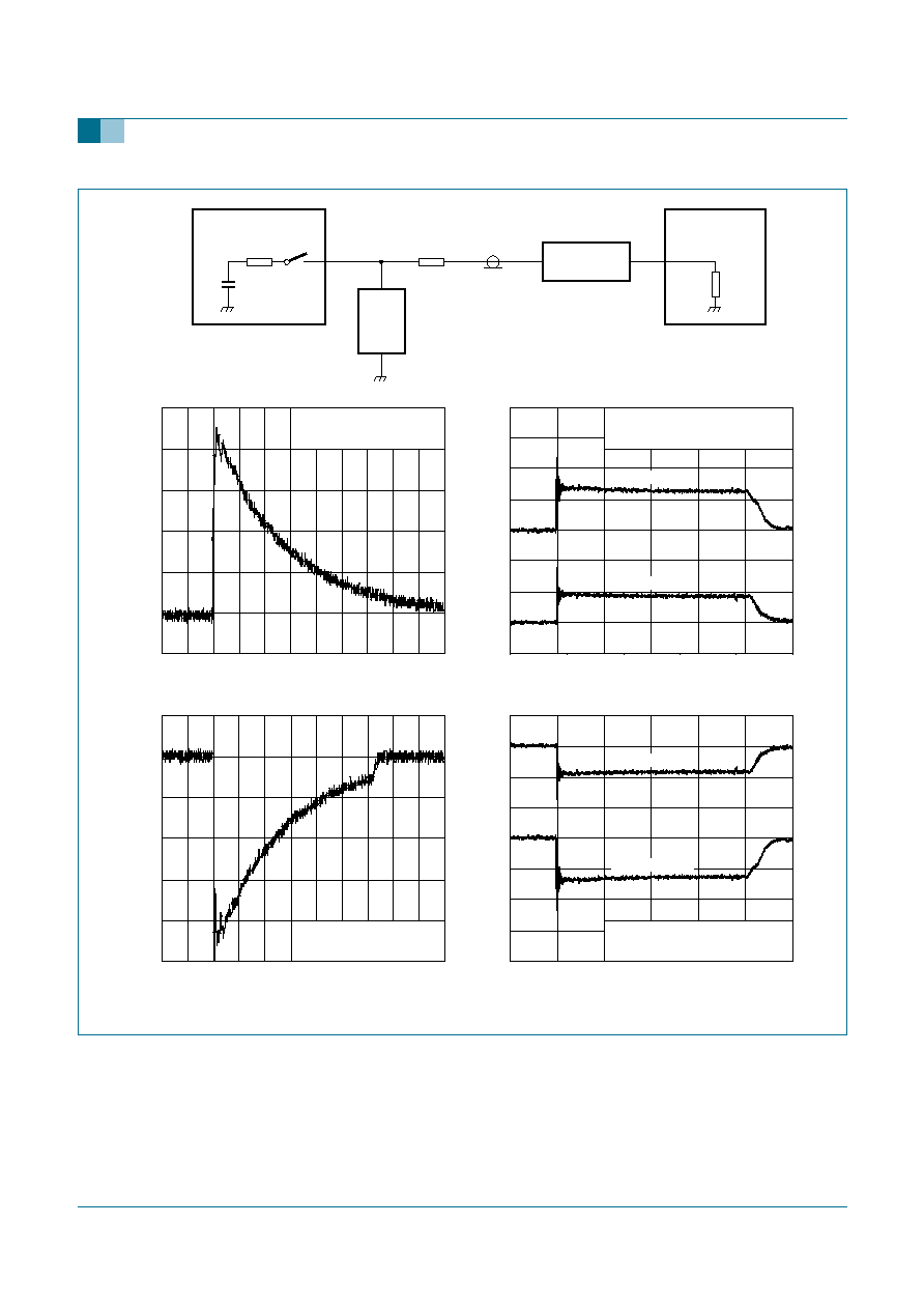
Fig 5.
ESD clamping test set-up and waveforms.
006aaa166
50
R
Z
C
Z
vertical scale = 200 V/div
horizontal scale = 50 ns/div
unclamped
+
1 kV ESD voltage waveform
(IEC 61000-4-2 network)
clamped
+
1 kV ESD voltage waveform
(IEC 61000-4-2 network)
unclamped
-
1 kV ESD voltage waveform
(IEC 61000-4-2 network)
clamped
-
1 kV ESD voltage waveform
(IEC 61000-4-2 network)
vertical scale = 20 V/div
horizontal scale = 50 ns/div
vertical scale = 200 V/div
horizontal scale = 50 ns/div
vertical scale = 20 V/div
horizontal scale = 50 ns/div
GND
GND
GND
GND
GND
GND
450
RG 223/U
50
coax
ESD TESTER
IEC 61000-4-2 network
C
Z
= 150 pF; R
Z
= 330
4 GHz DIGITAL
OSCILLOSCOPE
10
�
ATTENUATOR
D.U.T.
(Device
Under
Test)
PESD1LIN (15V)
PESD1LIN (15V)
PESD1LIN (24V)
PESD1LIN (24V)

9397 750 14032
� Koninklijke Philips Electronics N.V. 2004. All rights reserved.
Product data sheet
Rev. 01 -- 26 October 2004
7 of 12
Philips Semiconductors
PESD1LIN
LIN bus ESD protection diode in SOD323
7.
Application information
The PESD1LIN is designed for protection of one LIN bus signal line from the damage
caused by ElectroStatic Discharge (ESD) and surge pulses. The PESD1LIN provides a
surge capability of up to 160 W per line for a 8/20
�
s waveform.
Circuit board layout and protection device placement
Circuit board layout is critical for the suppression of ESD, Electrical Fast Transient (EFT)
and surge transients. The following guidelines are recommended:
1. Place the protection device as close to the input terminal or connector as possible.
2. The path length between the protection device and the protected line should be
minimized.
3. Keep parallel signal paths to a minimum.
4. Avoid running protection conductors in parallel with unprotected conductor.
5. Minimize all printed-circuit board conductive loops including power and ground loops.
6. Minimize the length of the transient return path to ground.
7. Avoid using shared transient return paths to a common ground point.
8. Ground planes should be used whenever possible. For multilayer printed-circuit
boards, use ground vias.
Fig 6.
Typical application: ESD protection of one automotive LIN bus line.
006aaa167
ground
PESD1LIN
24 V
15 V
line to be protected

Philips Semiconductors
PESD1LIN
LIN bus ESD protection diode in SOD323
9397 750 14032
� Koninklijke Philips Electronics N.V. 2004. All rights reserved.
Product data sheet
Rev. 01 -- 26 October 2004
8 of 12
8.
Package outline
Fig 7.
Package outline SOD323 (SC-76).
REFERENCES
OUTLINE
VERSION
EUROPEAN
PROJECTION
ISSUE DATE
IEC
JEDEC
JEITA
SOD323
SC-76
SOD323
99-09-13
03-12-17
Note
1. The marking bar indicates the cathode
UNIT
A
mm
0.05
1.1
0.8
0.40
0.25
0.25
0.10
1.8
1.6
1.35
1.15
2.7
2.3
0.45
0.15
A
1
max
DIMENSIONS (mm are the original dimensions)
Plastic surface mounted package; 2 leads
0
1
(1)
2
1
2 mm
scale
b
p
c
D
E
H
D
Q
0.25
0.15
L
p
v
0.2
A
D
A
E
L
p
b
p
detail X
A
1
c
Q
H
D
v
A
M
X

9397 750 14032
� Koninklijke Philips Electronics N.V. 2004. All rights reserved.
Product data sheet
Rev. 01 -- 26 October 2004
9 of 12
Philips Semiconductors
PESD1LIN
LIN bus ESD protection diode in SOD323
9.
Packing information
[1]
For further information and the availability of packing methods, see
Section 14
.
Table 9:
Packing methods
The indicated -xxx are the last three digits of the 12NC ordering code.
[1]
Type number
Package
Description
Packing quantity
3000
10000
PESD1LIN
SOD323
4 mm pitch, 8 mm tape and reel
-115
-135

9397 750 14032
� Koninklijke Philips Electronics N.V. 2004. All rights reserved.
Product data sheet
Rev. 01 -- 26 October 2004
10 of 12
Philips Semiconductors
PESD1LIN
LIN bus ESD protection diode in SOD323
10. Revision history
Table 10:
Revision history
Document ID
Release date
Data sheet status
Change notice
Doc. number
Supersedes
PESD1LIN_1
20041026
Product data sheet
-
9397 750 14032
-

Philips Semiconductors
PESD1LIN
LIN bus ESD protection diode in SOD323
9397 750 14032
� Koninklijke Philips Electronics N.V. 2004. All rights reserved.
Product data sheet
Rev. 01 -- 26 October 2004
11 of 12
11. Data sheet status
[1]
Please consult the most recently issued data sheet before initiating or completing a design.
[2]
The product status of the device(s) described in this data sheet may have changed since this data sheet was published. The latest information is available on the Internet at
URL http://www.semiconductors.philips.com.
[3]
For data sheets describing multiple type numbers, the highest-level product status determines the data sheet status.
12. Definitions
Short-form specification -- The data in a short-form specification is
extracted from a full data sheet with the same type number and title. For
detailed information see the relevant data sheet or data handbook.
Limiting values definition -- Limiting values given are in accordance with
the Absolute Maximum Rating System (IEC 60134). Stress above one or
more of the limiting values may cause permanent damage to the device.
These are stress ratings only and operation of the device at these or at any
other conditions above those given in the Characteristics sections of the
specification is not implied. Exposure to limiting values for extended periods
may affect device reliability.
Application information -- Applications that are described herein for any
of these products are for illustrative purposes only. Philips Semiconductors
make no representation or warranty that such applications will be suitable for
the specified use without further testing or modification.
13. Disclaimers
Life support -- These products are not designed for use in life support
appliances, devices, or systems where malfunction of these products can
reasonably be expected to result in personal injury. Philips Semiconductors
customers using or selling these products for use in such applications do so
at their own risk and agree to fully indemnify Philips Semiconductors for any
damages resulting from such application.
Right to make changes -- Philips Semiconductors reserves the right to
make changes in the products - including circuits, standard cells, and/or
software - described or contained herein in order to improve design and/or
performance. When the product is in full production (status `Production'),
relevant changes will be communicated via a Customer Product/Process
Change Notification (CPCN). Philips Semiconductors assumes no
responsibility or liability for the use of any of these products, conveys no
license or title under any patent, copyright, or mask work right to these
products, and makes no representations or warranties that these products are
free from patent, copyright, or mask work right infringement, unless otherwise
specified.
14. Contact information
For additional information, please visit: http://www.semiconductors.philips.com
For sales office addresses, send an email to: sales.addresses@www.semiconductors.philips.com
Level
Data sheet status
[1]
Product status
[2] [3]
Definition
I
Objective data
Development
This data sheet contains data from the objective specification for product development. Philips
Semiconductors reserves the right to change the specification in any manner without notice.
II
Preliminary data
Qualification
This data sheet contains data from the preliminary specification. Supplementary data will be published
at a later date. Philips Semiconductors reserves the right to change the specification without notice, in
order to improve the design and supply the best possible product.
III
Product data
Production
This data sheet contains data from the product specification. Philips Semiconductors reserves the
right to make changes at any time in order to improve the design, manufacturing and supply. Relevant
changes will be communicated via a Customer Product/Process Change Notification (CPCN).

� Koninklijke Philips Electronics N.V. 2004
All rights are reserved. Reproduction in whole or in part is prohibited without the prior
written consent of the copyright owner. The information presented in this document does
not form part of any quotation or contract, is believed to be accurate and reliable and may
be changed without notice. No liability will be accepted by the publisher for any
consequence of its use. Publication thereof does not convey nor imply any license under
patent- or other industrial or intellectual property rights.
Date of release: 26 October 2004
Document number: 9397 750 14032
Published in The Netherlands
Philips Semiconductors
PESD1LIN
LIN bus ESD protection diode in SOD323
15. Contents
1
Product profile . . . . . . . . . . . . . . . . . . . . . . . . . . 1
1.1
General description. . . . . . . . . . . . . . . . . . . . . . 1
1.2
Features . . . . . . . . . . . . . . . . . . . . . . . . . . . . . . 1
1.3
Applications . . . . . . . . . . . . . . . . . . . . . . . . . . . 1
1.4
Quick reference data. . . . . . . . . . . . . . . . . . . . . 1
2
Pinning information . . . . . . . . . . . . . . . . . . . . . . 2
3
Ordering information . . . . . . . . . . . . . . . . . . . . . 2
4
Marking . . . . . . . . . . . . . . . . . . . . . . . . . . . . . . . . 2
5
Limiting values. . . . . . . . . . . . . . . . . . . . . . . . . . 2
6
Characteristics . . . . . . . . . . . . . . . . . . . . . . . . . . 4
7
Application information. . . . . . . . . . . . . . . . . . . 7
8
Package outline . . . . . . . . . . . . . . . . . . . . . . . . . 8
9
Packing information. . . . . . . . . . . . . . . . . . . . . . 9
10
Revision history . . . . . . . . . . . . . . . . . . . . . . . . 10
11
Data sheet status . . . . . . . . . . . . . . . . . . . . . . . 11
12
Definitions . . . . . . . . . . . . . . . . . . . . . . . . . . . . 11
13
Disclaimers . . . . . . . . . . . . . . . . . . . . . . . . . . . . 11
14
Contact information . . . . . . . . . . . . . . . . . . . . 11