
Philips
Semiconductors
PDIUSBP11A
Universal Serial Bus Transceiver
Product specification
Supersedes data of 1997 Aug 01
1999 Jun 04
INTEGRATED CIRCUITS

Philips Semiconductors
Product specification
PDIUSBP11A
Universal Serial Bus transceiver
2
1999 Jun 04
853-2008 21712
FEATURES
À
Complies with Universal Serial Bus specification 1.1
À
Utilizes digital inputs and outputs to transmit and receive USB
cable data
À
Supports 12Mbit/s "Full Speed" and 1.5Mbit/s "Low Speed" serial
data transmission
À
Compatible with the VHDL "Serial Interface Engine" from USB
Implementers' Forum
À
Supports single-ended data interface
À
Single 3.3V supply
À
Available in SO-14, SSOP-14 and TSSOP-14 packages
DESCRIPTION
The PDIUSBP11A is a one chip generic USB transceiver. It is
designed to allow 5.0V or 3.3V programmable and standard logic to
interface with the physical layer of the Universal Serial Bus. It is
capable of transmitting and receiving serial data at both full speed
(12Mbit/s) and low speed (1.5Mbit/s) data rates.
The pinout conforms with the "Serial Interface Engine".
Implementation of the Serial Interface Engine along with the USB
transceiver allows the designer to make USB compatible devices
with off-the-shelf logic and easily modify and update the application.
The PDIUSBP11A is backward compatible to the PDIUSBP11 and
allows for single-ended data interfacing.
ORDERING INFORMATION
PACKAGES
TEMPERATURE RANGE
OUTSIDE NORTH AMERICA
NORTH AMERICA
PKG. DWG. #
14-pin plastic SO
¡40
░
C to +85
░
C
PDIUSBP11A D
PDIUSBP11A D
SOT108-1
14-pin plastic SSOP
¡40
░
C to +85
░
C
PDIUSBP11A DB
PDIUSBP11A DB
SOT337-1
14-pin plastic TSSOP
¡40
░
C to +85
░
C
PDIUSBP11APW
PDUSBP11APW DH
SOT402-1
PIN CONFIGURATION
8
1
2
3
4
5
6
7
9
10
11
12
13
14
MODE
OE#
RCV
VP
VM
SUSPND
GND
NC
SPEED
D¡
D
)
VPO
VMO/FSEO
VCC
SV00559
FUNCTIONAL DIAGRAM
D¡
D+
+
¡
OE#
SPEED
VMO/FSEO
VPO
RCV
VP
VM
SV00560

Philips Semiconductors
Product specification
PDIUSBP11A
Universal Serial Bus transceiver
1999 Jun 04
3
PIN DESCRIPTION
PIN
No.
PIN
SYMBOL
I/O
NAME AND FUNCTION
3
RCV
O
Receive data. CMOS level output for USB differential input
2
OE#
I
Output Enable. Active LOW, enables the transceiver to transmit data on the bus.
When not active the transceiver is in receive mode
1
MODE
I
Mode. When left unconnected, a weak pull-up transistor pulls it to V
CC
and in this
mode, the PDIUSBP11A is backward compatible to PDIUSBP11. When connected to
GND, the VMO/FSEO pin takes the function of FSEO (Force SEO).
Inputs to differential driver. (Outputs from SIE).
MODE
VPO
VMO/FSEO
RESULT
0
0
0
Logic "0"
0
1
SE0#
12, 13
V
PO
, V
MO
/F
SEO
I
1
0
Logic "1"
12, 13
V
PO
, V
MO
/F
SEO
I
1
1
SEO#
1
0
0
SE0#
0
1
Logic "0"
1
0
Logic "1"
1
1
Illegal code
Gated version of D¡ and D+. Outputs are logic "0" and logic "1". Used to detect single
ended zero (SE0#), error conditions, and interconnect speed. (Inputs to SIE).
VP
VM
RESULT
4, 5
V
P
, V
M
O
0
0
SE0#
0
1
Low Speed
1
0
Full Speed
1
1
Error
11, 10
D+, D¡
AI/O
Data+, Data¡. Differential data bus conforming to the Universal Serial Bus standard.
6
SUSPND
I
Suspend. Enables a low power state while the USB bus is inactive. While the suspnd
pin is active it will drive the RCV pin to a logic "0" state. Both D+ and D¡ are tri-stated.
9
SPEED
I
Edge rate control. Logic "1" operates at edge rates for "full speed". Logic "0" operates
edge rates for "low speed".
14
V
CC
3.0V to 3.6V power supply
7
GND
Ground reference

Philips Semiconductors
Product specification
PDIUSBP11A
Universal Serial Bus transceiver
1999 Jun 04
4
RECOMMENDED OPERATING CONDITIONS
SYMBOL
PARAMETER
CONDITIONS
LIMITS
UNIT
SYMBOL
PARAMETER
CONDITIONS
MIN
MAX
UNIT
MIN.
MAX.
V
CC
DC supply voltage
3.0
3.6
V
V
I
DC Input voltage range
0
5.5
V
V
AI/O
DC input range for AI/O's
0
V
CC
V
V
O
DC output voltage range
0
V
CC
V
T
amb
Operating ambient temperature range in free air
See DC and AC characteristics
per device
¡40
+85
░
C
ABSOLUTE MAXIMUM RATINGS
1
In accordance with the Absolute Maximum Rating System (IEC 134) Voltages are referenced to GND (ground = 0V)
SYMBOL
PARAMETER
CONDITIONS
LIMITS
UNIT
SYMBOL
PARAMETER
CONDITIONS
MIN
MAX
UNIT
V
CC
DC supply voltage
¡0.5
+6.5
V
I
latchup
Latchup current
V
I
< 0 or V
I
> V
CC
¡
200
mA
V
I
DC input voltage
Note 2
¡0.5
+5.5
V
V
I/O
DC input voltage range for I/O's
¡0.5
V
CC
+0.5
V
V
O
DC output voltage
Note 2
¡0.5
V
CC
+0.5
V
I
CC
, I
GND
DC V
CC
or GND current
¡
▒
100
mA
T
STO
Storage temperature range
¡60
+150
░
C
P
TOT
Power dissipation per package
mW
NOTES:
1. Stresses beyond those listed may cause permanent damage to the device. These are stress ratings only and functional operation of the
device at these or any other conditions beyond those indicated under "recommended operating conditions" is not implied. Exposure to
absolute-maximum-rated conditions for extended periods may affect device reliability.
2. The input and output voltage ratings may be exceeded if the input and output clamp current ratings are observed.
Philips Semiconductors
Product specification
PDIUSBP11A
Universal Serial Bus transceiver
1999 Jun 04
5
DC CHARACTERISTICS (DIGITAL PINS)
LIMITS
SYMBOL
PARAMETER
TEST CONDITIONS
Temp = ¡40
░
C to +85
░
C
UNIT
MIN
TYP
MAX
INPUT LEVELS
V
IL
LOW level input voltage
0.8
V
V
IH
HIGH level input voltage
2.0
V
OUTPUT LEVELS
V
O
LOW level output voltage
I
OL
= 4mA
0.4
V
V
OL
LOW level output voltage
I
OL
= 20
Á
A
0.1
V
V
O
HIGH level output voltage
I
OH
= 4mA
2.4
V
V
OH
HIGH level output voltage
I
OH
= 20
Á
A
V
CC
¡0.1
V
LEAKAGE CURRENT
I
L
Input leakage current
▒
5
Á
A
I
CCS
Supply current in Suspend
¡
5
Á
A
SUPPLY CURRENT
I
CC
Operating supply current
¡
6
¡
mA
DC CHARACTERISTICS (AI/O PINS)
LIMITS
SYMBOL
PARAMETER
TEST CONDITIONS
Temp = ¡40
░
C to +85
░
C
UNIT
MIN
MAX
INPUT LEVELS
V
DI
Differential input sensitivity
|(D+) ¡ (D¡)|
0.2
V
V
CM
Differential common mode range
Includes V
DI
range
0.8
2.5
V
V
SE
Single ended receiver threshold
0.8
2.0
V
OUTPUT LEVELS
V
OL
Static output LOW voltage
R
L
of 1.5 k
to 3.6V
0.3
V
V
OH
Static output HIGH voltage
R
L
of 15 k
to GND
2.8
3.6
V
LEAKAGE CURRENT
I
LO
Hi-Z State data line leakage current
0V
<
V
IN
<
3.3V
▒
10
Á
A
CAPACITANCE
C
IN
Transceiver capacitance
Pin to GND
20
pF
OUTPUT RESISTANCE
Z
DRV
1
Driver output resistance
Steady state drive
6
18
NOTE:
1. Excludes external resistor. In order to comply with USB Specifications 1.1, external series resistors of 24
▒
1% each on D+ and D¡ are
recommended.
Philips Semiconductors
Product specification
PDIUSBP11A
Universal Serial Bus transceiver
1999 Jun 04
6
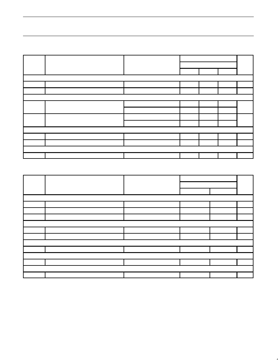
AC CHARACTERISTICS (AI/O PINS. FULL SPEED)
LIMITS
SYMBOL
PARAMETER
TEST CONDITIONS
T
amb
= ¡40
░
C to +85
░
C
UNIT
MIN
TYP
MAX
Driver Characteristics
C
L
= 50pF;
R
pu
= 1.5k
on D+ to V
CC
Transition Time:
Between 10% and 90%
t
R
Rise time
Waveform 1
4
1
20
ns
t
F
Fall time
Waveform 1
4
1
20
ns
t
RFM
Rise / Fall time matching
(t
R
/t
F
)
90
111.1
%
V
CRS
Output signal crossover voltage
1.3
2.0
V
Driver Timings
tp
LH
Driver propagation delay
Waveform 2
18
ns
tp
HL
(VPO, VMO/FSEO to D+/D¡)
Waveform 2
19
ns
tp
HZ
Driver disable delay
Waveform 4
13
ns
tp
LZ
(OE# to D+/D¡)
Waveform 4
13
ns
tp
ZH
Driver enable delay
Waveform 4
17
ns
tp
ZL
(OE# to D+/D¡)
Waveform 4
17
ns
Receiver Timings
tp
LH
Receiver propagation delay
Waveform 3
16
ns
tp
HL
(D+, D¡ to RCV)
Waveform 3
19
ns
tp
LH
Single-ended receiver delay
Waveform 3
8
ns
tp
HL
(D+, D¡ to VP, VM)
Waveform 3
8
ns
NOTE:
1. The 4ns specification is only for 0
░
C to +85
░
C.
AC CHARACTERISTICS (AI/O PINS. LOW SPEED)
LIMITS
SYMBOL
PARAMETER
TEST CONDITIONS
T
amb
= ¡40
░
C to +85
░
C
UNIT
MIN
TYP
MAX
Driver Characteristics
C
L
= 200pF and 600pF;
R
pu
= 1.5k
on D¡ to V
CC
Transition Time:
Between 10% and 90%
t
LR
Rise time
C
L
= 200pF. Waveform 1
75
ns
t
LR
Rise time
C
L
= 600pF. Waveform 1
300
ns
t
LF
Fall time
C
L
= 200pF. Waveform 1
75
ns
t
LF
Fall time
C
L
= 600pF. Waveform 1
300
ns
t
LRFM
Rise / Fall time matching
(t
LR
/t
LF
)
80
125
%
V
LCRS
Output signal crossover voltage
1.3
2.0
V
Driver Timings
tp
LH
Driver propagation delay
Waveform 2
300
ns
tp
HL
(VPO, VMO/FSEO to D+/D¡)
Waveform 2
300
ns
tp
HZ
Driver disable delay
Waveform 4
13
ns
tp
LZ
(OE# to D+/D¡)
Waveform 4
13
ns
tp
ZH
Driver enable delay
Waveform 4
205
ns
tp
ZL
(OE# to D+/D¡)
Waveform 4
205
ns
Receiver Timings
tp
LH
Receiver propagation delay
Waveform 3
18
ns
tp
HL
(D+, D¡ to RCV)
Waveform 3
18
ns
tp
LH
Single-ended receiver delay
Waveform 3
28
ns
tp
HL
(D+, D¡ to VP, VM)
Waveform 3
28
ns

Philips Semiconductors
Product specification
PDIUSBP11A
Universal Serial Bus transceiver
1999 Jun 04
7
AC WAVEFORMS
V
OL
and V
OH
are the typical output voltage drops that occur with the
output load. (V
CC
never goes below 3.0V).
V
OH
V
OL
90%
90%
t
RISE
t
FALL
SV00186
10%
10%
Waveform 1. Rise and Fall Times
t
PHL
t
PLH
D+
D¡
V
CR
GND
2.7V
V
CR
1.5V
1.5V
INPUT
SV00598
Waveform 2. VPO, VMO/FSEO to D+/D¡
t
PHL
t
PLH
V
OH
V
OL
1.5V
D¡
D+
1.5V
V
CR
2.0V
1.0V
V
CR
SV00599
Waveform 3. D+/D¡ to RCV, VP/VM
t
PHZ
t
PLZ
t
PZH
t
PZL
V
OH
V
OL
V
M
0V
2.7V
0.5V
CC
1.5V
1.5V
OE#
0.5V
CC
V
OH
¡0.3
V
OL
+0.3
D+/D¡
SV00597
Waveform 4. OE# to D+/D¡
TEST CIRCUITS AND WAVEFORMS
SV00149
D.U.T.
Test Point
25pF
Load for VM/VP and RCV
SV00150
D.U.T.
Test Point
50pF
+
¡
24
500
V
V = 0 for t
PZH
, t
PHZ
V = V
CC
for t
PZL
, t
PLZ
Load for Enable and Disable Times
SV01097
D.U.T.
Test Point
24
V
CC
1.5k
*
S1
C
L
= 50pF, Full Speed
C
L
= 200pF, Low Speed (Min Timing)
C
L
= 600pF, Low Speed (Max Timing)
* 1.5K
on D¡ (Low Speed) or D+ (Full Speed) Only
Test
S1
D¡/LS
D+/LS
D¡/FS
D+/FS
close
open
open
close
15k
C
L
Load for D+/D¡
Philips Semiconductors
Poduct specification
PDIUSBP11A
Universal Serial Bus Transceiver
1999 Jun 04
8
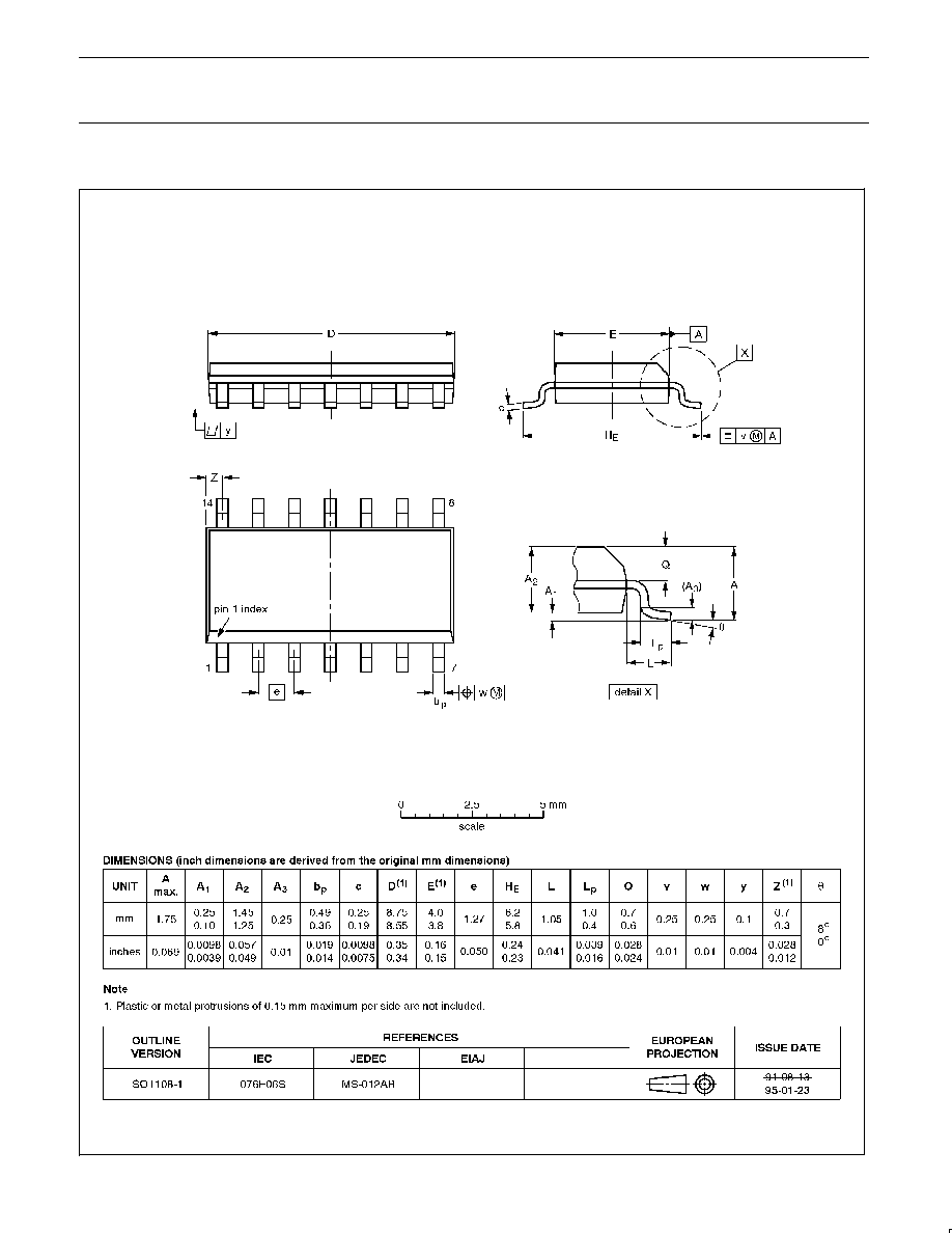
SO14:
plastic small outline package; 14 leads; body width 3.9 mm
SOT108-1
Philips Semiconductors
Poduct specification
PDIUSBP11A
Universal Serial Bus Transceiver
1999 Jun 04
9
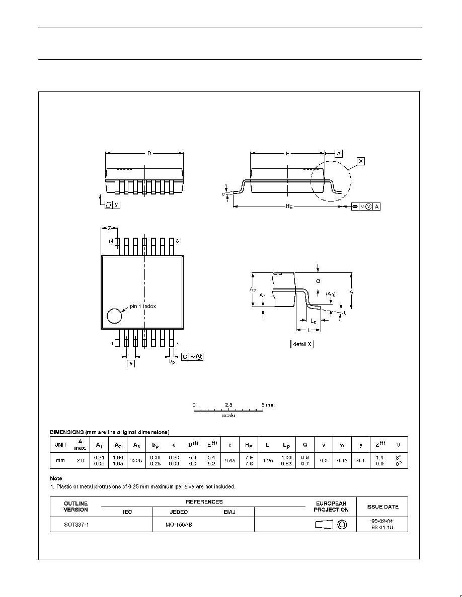
SSOP14:
plastic shrink small outline package; 14 leads; body width 5.3 mm
SOT337-1
Philips Semiconductors
Poduct specification
PDIUSBP11A
Universal Serial Bus Transceiver
1999 Jun 04
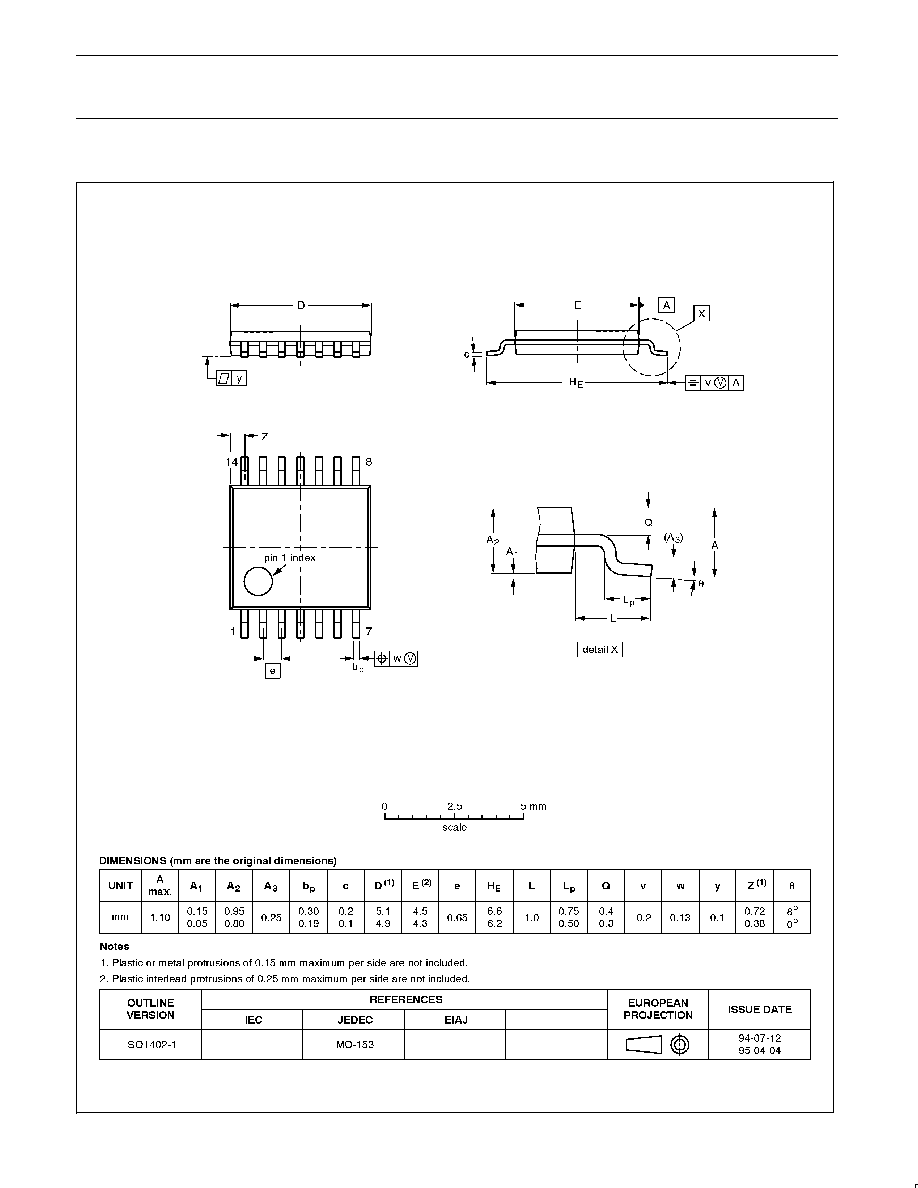
10
TSSOP14:
plastic thin shrink small outline package; 14 leads; body width 4.4 mm
SOT402-1

Philips Semiconductors
Poduct specification
PDIUSBP11A
Universal Serial Bus Transceiver
1999 Jun 04
11
NOTES

Philips Semiconductors
Poduct specification
PDIUSBP11A
Universal Serial Bus Transceiver
1999 Jun 04
12
Definitions
Short-form specification -- The data in a short-form specification is extracted from a full data sheet with the same type number and title. For
detailed information see the relevant data sheet or data handbook.
Limiting values definition -- Limiting values given are in accordance with the Absolute Maximum Rating System (IEC 134). Stress above one
or more of the limiting values may cause permanent damage to the device. These are stress ratings only and operation of the device at these or
at any other conditions above those given in the Characteristics sections of the specification is not implied. Exposure to limiting values for extended
periods may affect device reliability.
Application information -- Applications that are described herein for any of these products are for illustrative purposes only. Philips
Semiconductors make no representation or warranty that such applications will be suitable for the specified use without further testing or
modification.
Disclaimers
Life support -- These products are not designed for use in life support appliances, devices or systems where malfunction of these products can
reasonably be expected to result in personal injury. Philips Semiconductors customers using or selling these products for use in such applications
do so at their own risk and agree to fully indemnify Philips Semiconductors for any damages resulting from such application.
Right to make changes -- Philips Semiconductors reserves the right to make changes, without notice, in the products, including circuits, standard
cells, and/or software, described or contained herein in order to improve design and/or performance. Philips Semiconductors assumes no
responsibility or liability for the use of any of these products, conveys no license or title under any patent, copyright, or mask work right to these
products, and makes no representations or warranties that these products are free from patent, copyright, or mask work right infringement, unless
otherwise specified.
Philips Semiconductors
811 East Arques Avenue
P.O. Box 3409
Sunnyvale, California 94088¡3409
Telephone 800-234-7381
®
Copyright Philips Electronics North America Corporation 1999
All rights reserved. Printed in U.S.A.
Date of release: 06-99
Document order number:
9397 750 06063
Philips
Semiconductors
Data sheet
status
Objective
specification
Preliminary
specification
Product
specification
Product
status
Development
Qualification
Production
Definition
[1]
This data sheet contains the design target or goal specifications for product development.
Specification may change in any manner without notice.
This data sheet contains preliminary data, and supplementary data will be published at a later date.
Philips Semiconductors reserves the right to make chages at any time without notice in order to
improve design and supply the best possible product.
This data sheet contains final specifications. Philips Semiconductors reserves the right to make
changes at any time without notice in order to improve design and supply the best possible product.
Data sheet status
[1]
Please consult the most recently issued datasheet before initiating or completing a design.