Document Outline
- FEATURES
- DESCRIPTION
- ORDERING INFORMATION
- BLOCK DIAGRAM
- Analog Transceivers
- Hub Repeater
- End of Frame Timers
- General and Individual Port Controller
- Bit Clock Recovery
- Philips Serial Interface Engine (PSIE)
- Memory Management Unit (MMU) and Integrated RAM
- I 2 C Slave Interface
- ENDPOINT DESCRIPTIONS
- PIN DESCRIPTION
- APPLICATION DIAGRAM
- I 2 C Interface.
- Protocol
- Timing
- ADDRESS TABLE
- COMMAND SUMMARY
- COMMAND DESCRIPTIONS
- Command Procedure
- Initialization Commands
- Data Flow Commands
- Hub Commands
- GENERAL COMMANDS
- EMBEDDED FUNCTION
- Host Requests
- Babbling Condition
- Remote WakeUp
- RECOMMENDED OPERATING CONDITIONS
- ABSOLUTE MAXIMUM RATINGS
- DC CHARACTERISTICS (DIGITAL PINS)
- DC CHARACTERISTICS (AI/O PINS)
- LOAD FOR D+/D…
- AC CHARACTERISTICS
- AI/O PINS. FULL SPEED
- AI/O PINS. LOW SPEED
- I 2 C
- PACKAGE OUTLINES
- DEFINITIONS

Philips
Semiconductors
PDIUSBH11
Universal Serial Bus Hub
Product specification
Supersedes data of 1997 Apr 17
1997 Aug 01
INTEGRATED CIRCUITS

Philips Semiconductors
Product specification
PDIUSBH11
Universal Serial Bus Hub
2
1997 Aug 01
8531968 18238
FEATURES
·
Complies with the Universal Serial Bus specification Rev. 1.0
·
Four downstream ports with per packet connectivity
·
Embedded function with two endpoints (control and interrupt)
·
Integrated FIFO memory for hub and embedded function
·
Automatic protocol handling
·
Versatile I
2
C interface
·
Allows software control of monitor
·
Compliant with USB Human Interface and Display Device Class
·
Single 3.3V supply with 5V tolerant I/O
DESCRIPTION
The Philips Semiconductors PDIUSBH11 is a compound USB hub
IC (hub plus embedded function).
It is used in a microcontroller based system and communicates with
the system microcontroller over the I
2
C serial bus. This modular
approach to implementing a hub and embedded function allows the
designer to maintain the system microcontroller of choice and retain
existing architecture. This cuts down development time and offers
the most cost-effective solution.
Ideal applications for the IC include computer monitors and
keyboards.
The PDIUSBH11 conforms to the USB specification 1.0 and I
2
C
serial interface specification. It is also compliant with the USB
Human Input Device and Monitor Control Class specifications.
The embedded function of the PDIUSBH11 appears as PORT1 to
the host system and the four downstream ports are numbered 2
through 5.
ORDERING INFORMATION
PACKAGES
TEMPERATURE RANGE
OUTSIDE NORTH AMERICA
NORTH AMERICA
PKG. DWG. #
32-pin plastic SO
0
°
C to +70
°
C
PDIUSBH11 D
PDIUSBH11 D
SOT287-1
32-pin plastic SDIP
0
°
C to +70
°
C
PDIUSBH11 NB
PDIUSBH11 NB
SOT232-1
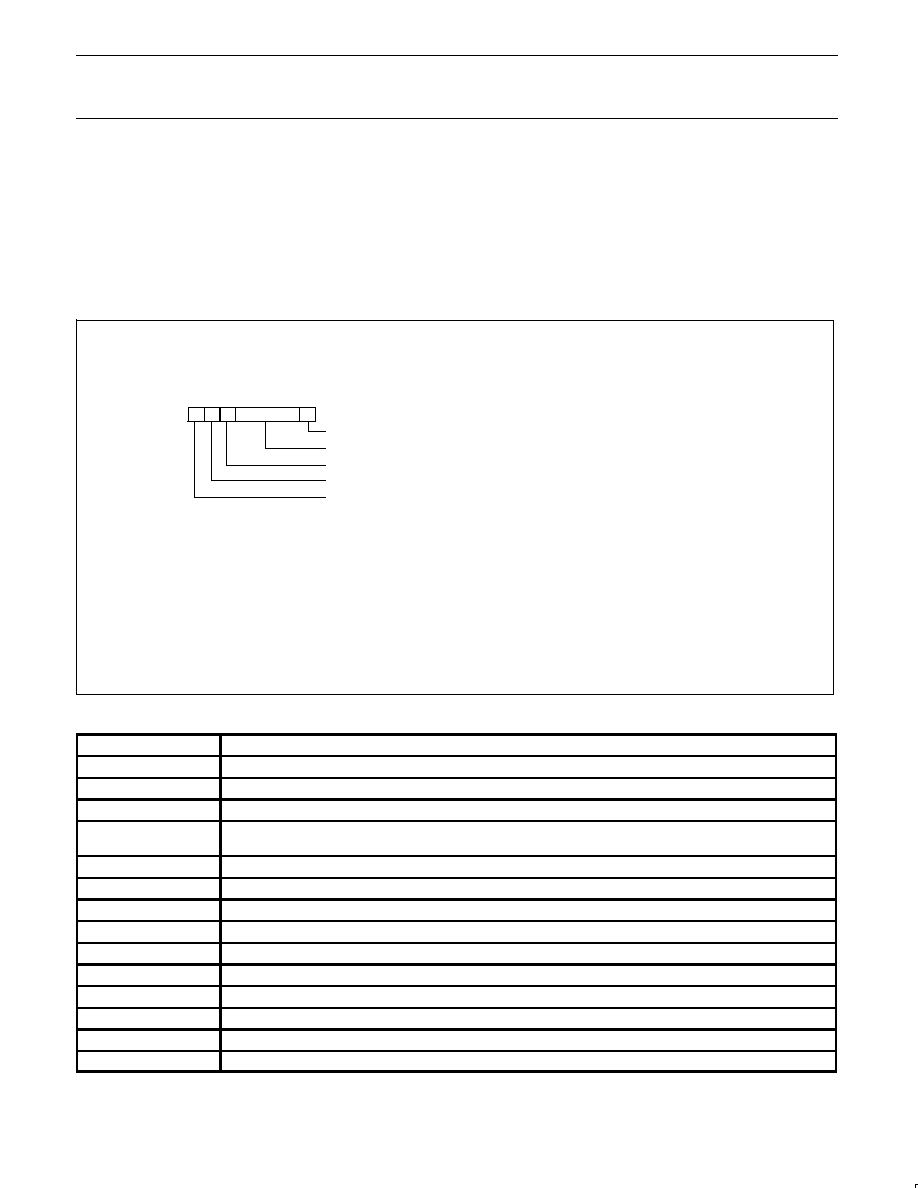
BLOCK DIAGRAM
ANALOG
T
X
/R
X
PORT
CONTROL
ANALOG
T
X
/R
X
PORT
CONTROL
ANALOG
T
X
/R
X
PORT
CONTROL
ANALOG
T
X
/R
X
PORT
CONTROL
GENERAL
PORT
CONTROLLER
HUB
REPEATER
END OF
FRAME
TIMERS
ANALOG
T
X
/R
X
PHILIPS
SIE
INTEGRATED
RAM
BIT CLOCK
RECOVERY
MEMORY
MANAGEMENT
UNIT
I
2
C
SLAVE
INTERFACE
48 MHz
FULL SPEED
INTERRUPT
SDA
SCL
LED
ENABLE
D
D+
LED
ENABLE
D
D+
LED
ENABLE
D
D+
LED
ENABLE
D
D+
DOWNSTREAM
PORT 2
DOWNSTREAM
PORT 3
DOWNSTREAM
PORT 4
DOWNSTREAM
PORT 5
D+
D
UPSTREAM
PORT
SV00226
NOTE:
1. This is a conceptual block diagram and does not include each individual signal.

Philips Semiconductors
Product specification
PDIUSBH11
Universal Serial Bus Hub
1997 Aug 01
3
Analog Transceivers
These transceivers interface directly to the USB cables through
some termination resistors. They are capable of transmitting and
receiving serial data at both "full speed" (12 Mbit/s) and "low speed"
(1.5 Mbit/s) data rates.
Hub Repeater
The hub repeater is responsible for managing connectivity on a per
packet basis. It implements packet signaling connectivity and
resume connectivity.
Low speed devices can be connected to downstream ports since the
repeater will not propagate upstream packets to downstream ports,
to which low speed devices are connected, unless they are
preceded by a PREAMBLE PID.
End of Frame Timers
This block contains the specified EOF1 and EOF2 timers which are
used to detect loss-of-activity and babble error conditions in the hub
repeater. The timers also maintain the low-speed keep-alive strobe
which is sent at the beginning of a frame.
General and Individual Port Controller
The general and individual port controllers together provide status
and control of individual downstream ports. Via the I
2
C-interface a
microcontroller can access the downstream ports and request or
change the status of each individual port.
Any change in the status or settings of the individual port will result
in an interrupt request. Via an interrupt register, the servicing
microcontroller can look up the downstream port which generated
the interrupt and request its new status. Any port status change can
then be reported to the host via the hub status change (interrupt)
endpoint.
Bit Clock Recovery
The bit clock recovery circuit recovers the clock from the incoming
USB data stream using (4X) over-sampling principle. It is able to
track jitter and frequency drift specified by the USB spec.
Philips Serial Interface Engine (PSIE)
The Philips SIE implements the full USB protocol layer. It is
completely hardwired for speed and needs no firmware intervention.
The functions of this block include: synchronization pattern
recognition, parallel / serial conversion, bit stuffing / destuffing, CRC
checking / generation, PID verification / generation, address
recognition, handshake evaluation / generation.
Memory Management Unit (MMU) and Integrated RAM
The MMU and the integrated RAM is used to handle the large
difference in data-rate between USB, running in burst of 12 Mbit/s
and the I
2
C interface to the microcontroller, running at 100 kbit/s.
This allows the microcontroller to read and write USB packets at its
own (low) speed through I
2
C.
I
2
C Slave Interface
This block implements the necessary I
2
C interface protocol. A slave
I
2
C allows for simple micro-coding. An interrupt is used to alert the
microcontroller whenever the PDIUSBH11 needs attention. As a
slave I
2
C device, the PDIUSBH11 I
2
C clock: SCL is an input and is
controlled by the microcontroller.
ENDPOINT DESCRIPTIONS
The following table summarizes the endpoints supported by the PDIUSBH11.
FUNCTION
ENDPOINT
NUMBER
ENDPOINT TYPE
TRANSFER TYPE
DIRECTION
MAXIMUM PACKET SIZE
(bytes)
HUB
0
Default
Control
IN, OUT
8
HUB
1
Status change
Interrupt
IN
1
EMBEDDED
0
Default
Control
IN, OUT
8
1
Interrupt
Interrupt
IN
8
PIN DESCRIPTION
The PDIUSBH11 has two modes of operation. The first mode
(Mode 0) enables the pins DNx_EN_N to power a LED indicating
the port is enabled. The second mode (Mode 1) utilizes the LED
enable pins as per port overcurrent condition pins.
The voltage level at power up on the TEST1 and TEST2 pins
determine the PDIUSBH11 mode of operation. When both of the
pins are connected to Ground, Mode 0 is enabled. When pins
TEST1 and TEST2 are connected to Vcc, Mode 1 is enabled. Note
that in Mode 1 the pin DN2_EN_N remains an LED enable pin. Pin
TEST3 should always be connected to Ground at all times.

Philips Semiconductors
Product specification
PDIUSBH11
Universal Serial Bus Hub
1997 Aug 01
4
PIN DESCRIPTION (MODE 0)
PIN NO
PIN SYMBOL
I/O
DRIVE
NAME AND FUNCTION
1
TEST1
I
Connect to Ground
2
TEST2
I
Connect to Ground
3
TEST3
I
Connect to Ground
4
RESET_N
I
ST
Power-on reset
5
GND
POWER
Ground reference
6
XTAL1
I/O
Crystal connection 1 (48MHz)
7
XTAL2
I/O
Crystal connection 2 (48MHz)
8
CLK12MHZ
O
2mA
12MHz output clock for external devices
9
V
CC
POWER
Voltage supply 3.3V
"
0.3V
10
OCURRENT_N
I
ST
Over-current notice to the device
11
SWITCH_N
O
OD8
Enables power to downstream ports
12
SUSPEND
O
4mA
Device is in suspended state
13
DN2_EN_N
O
OD8
Downstream port 2 LED enable indicator
14
DN3_EN_N
O
OD8
Downstream port 3 LED enable indicator
15
DN4_EN_N
O
OD8
Downstream port 4 LED enable indicator
16
DN5_EN_N
O
OD8
Downstream port 5 LED enable indicator
17
INT_N
O
OD4
Connect to microcontroller interrupt
18
SDA
I/O
OD4
I
2
C bi-directional data
19
SCL
I/O
OD4
I
2
C bit-clock
20
GND
POWER
Ground reference
21
DN5_DP
AI/O
Downstream port 5 D
+
connection
22
DN5_DM
AI/O
Downstream port 5 D
connection
23
DN4_DP
AI/O
Downstream port 4 D
+
connection
24
DN4_DM
AI/O
Downstream port 4 D
connection
25
DN3_DP
AI/O
Downstream port 3 D
+
connection
26
DN3_DM
AI/O
Downstream port 3 D
connection
27
DN2_DP
AI/O
Downstream port 2 D
+
connection
28
DN2_DM
AI/O
Downstream port 2 D
-
connection
29
AGND
POWER
Analog Ground reference
30
AV
CC
POWER
Analog voltage supply 3.3V
"
0.3V
31
UP_DP
AI/O
Upstream D
+
connection
32
UP_DM
AI/O
Upstream D
-
connection

Philips Semiconductors
Product specification
PDIUSBH11
Universal Serial Bus Hub
1997 Aug 01
5
PIN DESCRIPTION (MODE 1)
PIN NO
PIN SYMBOL
I/O
DRIVE
NAME AND FUNCTION
1
TEST1
I
Connect to V
CC
2
TEST2
I
Connect to V
CC
3
TEST3
I
Connect to Ground
4
RESET_N
I
ST
Power-on reset
5
GND
POWER
Ground reference
6
XTAL1
I/O
Crystal connection 1 (48MHz)
7
XTAL2
I/O
Crystal connection 2 (48MHz)
8
CLK12MHZ
O
2mA
12MHz output clock for external devices
9
V
CC
POWER
Voltage supply 3.3V
"
0.3V
10
OCURRENT2_N
I
ST
Downstream port 2 over-current notice
11
SWITCH_N
O
OD8
Enables power to downstream ports
12
SUSPEND
O
4mA
Device is in suspended state
13
DN2_EN_N
O
OD8
Downstream port 2 LED enable indicator
14
OCURRENT3_N
I
ST
Downstream port 3 over-current notice
15
OCURRENT4_N
I
ST
Downstream port 4 over-current notice
16
OCURRENT5_N
I
ST
Downstream port 5 over-current notice
17
INT_N
O
OD4
Connect to microcontroller interrupt
18
SDA
I/O
OD4
I
2
C bi-directional data
19
SCL
I/O
OD4
I
2
C bit-clock
20
GND
POWER
Ground reference
21
DN5_DP
AI/O
Downstream port 5 D
+
connection
22
DN5_DM
AI/O
Downstream port 5 D
connection
23
DN4_DP
AI/O
Downstream port 4 D
+
connection
24
DN4_DM
AI/O
Downstream port 4 D
-
connection
25
DN3_DP
AI/O
Downstream port 3 D
+
connection
26
DN3_DM
AI/O
Downstream port 3 D
-
connection
27
DN2_DP
AI/O
Downstream port 2 D
+
connection
28
DN2_DM
AI/O
Downstream port 2 D
-
connection
29
AGND
POWER
Analog Ground reference
30
AV
CC
POWER
Analog voltage supply 3.3V
"
0.3V
31
UP_DP
AI/O
Upstream D
+
connection
32
UP_DM
AI/O
Upstream D
-
connection
NOTES:
1. Signals ending in _N indicate active low signals.
ST: Schmitt Trigger
OD4, OD8: Open Drain with 4 or 8 mA drive
AI/O: Analog I/O

Philips Semiconductors
Product specification
PDIUSBH11
Universal Serial Bus Hub
1997 Aug 01
6
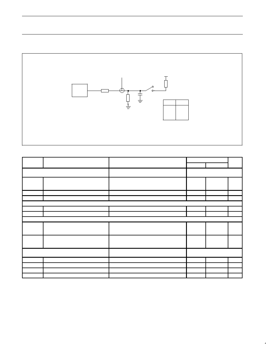
APPLICATION DIAGRAM
I
2
C
ENABLE LED
POWER SWITCH
AND
OVERCURRENT CIRCUIT
5V
SWITCHED
5V
H11
µ
C
12MHz
48MHz
USB
DOWNSTREAM
USB
UPSTREAM
3.3V
SV00227
I
2
C Interface
.
The I
2
C bus is used to interface to an external microcontroller
needed to control the operation of the hub. For cost consideration,
the target system microcontroller can be shared and utilized for this
purpose. The PDIUSBH11 implements a slave I
2
C interface. When
the PDIUSBH11 needs to communicate with the microcontroller it
asserts an interrupt signal. The microcontroller services this
interrupt by reading the appropriate status register on the
PDIUSBH11 through the I
2
C bus. (For more information about the
I
2
C serial bus, refer to the I
2
C handbook, Philips order number 9397
750 00013).
The I
2
C interface on the PDIUSBH11 defines two types of
transactions :
1. command transaction
A command transaction is used to define which data (e.g., status
byte, buffer data, ...) will be read from / written to the USB
interface in the next data transaction. A data transaction usually
follows a command transaction.
2. data transaction
A data transaction reads data from / writes data to the USB
interface. The meaning of the data is dependent on the
command transaction which was sent before the data
transaction.
Two addresses are used to differentiate between command and
data transactions. Writing to the command address is interpreted as
a command, while reading from / writing to the data address is used
to transfer data between the PDIUSBH11 and the controller.
ADDRESS TABLE
TYPE OF ADDRESS
PHYSICAL ADDRESS
(MSB to LSB)
Command
0011 011 (binary)
Data
0011 010 (binary)
Protocol
An I
2
C transaction starts with a `Start Condition', followed by an
address. When the address matches either the command or data
address the transaction starts and runs until a `Stop Condition' or
another `Start Condition' (repeated start) occurs.
The command address is write-only and is unable to do a read. The
next bytes in the message are interpreted as commands. Several
command bytes can be sent after one command address. Each of
the command bytes is acknowledged and passed on to the Memory
Management Unit inside the PDIUSBH11.
When the start condition address matches the data address, the
next bytes are interpreted as data. When the RW bit in the address
indicates a `master writes data to slave' (=`0') the bytes are received,
acknowledged and passed on to the Memory Management Unit. If
the RW bit in the address indicates a `master reads data from slave'
(=`1') the PDIUSBH11 will send data to the master. The I
2
C-master
must acknowledge all data bytes except the last one. In this way the
I
2
C interface knows when the last byte has been transmitted and it
then releases the SDA line so that the master controller can
generate the STOP condition.
Repeated start support allows another packet to be sent without
generating a Stop Condition.
Timing
When the master writes data to the PDIUSBH11, the data is
sampled 1 micro-second after the rising edge of SCL. When the
PDIUSBH11 writes data to the master, the data is driven 1
micro-second after the falling edge of SCL.

Philips Semiconductors
Product specification
PDIUSBH11
Universal Serial Bus Hub
1997 Aug 01
7
COMMAND SUMMARY
Some commands have the same command code (e.g., Read Buffer and Write Buffer). In these cases, the direction of the Data Phase (read or
write) indicates which command is executed.
COMMAND NAME
RECIPIENT
CODING
DATA PHASE
Initialization Commands
Set Address / Enable
Hub
D0h
Write 1 byte
Embedded Function
D1h
Write 1 byte
Set Endpoint Enable
Hub + Embedded Function
D8h
Write 1 byte
Data Flow Commands
Read Interrupt Register
F4h
Read 1 byte
Select Endpoint
Hub Control OUT
00h
Read 1 byte (optional)
Hub Control IN
01h
Read 1 byte (optional)
Embedded Function Control OUT
02h
Read 1 byte (optional)
Embedded Function Control IN
03h
Read 1 byte (optional)
Embedded Function Interrupt
04h
Read 1 byte (optional)
Read Last Transaction Status
Hub Control OUT
40h
Read 1 byte
Hub Control IN
41h
Read 1 byte
Embedded Function Control OUT
42h
Read 1 byte
Embedded Function Control IN
43h
Read 1 byte
Embedded Function Interrupt
44h
Read 1 byte
Read Endpoint Status
Hub Control OUT
80h
Read 1 byte
Hub Control IN
81h
Read 1 byte
Embedded Function Control OUT
82h
Read 1 byte
Embedded Function Control IN
83h
Read 1 byte
Embedded Function Interrupt
84h
Read 1 byte
Read Buffer
Selected Endpoint
F0h
Read n bytes
Write Buffer
Selected Endpoint
F0h
Write n bytes
Set Endpoint Status
Hub Control OUT
40h
Write 1 byte
Hub Control IN
41h
Write 1 byte
Embedded Function Control OUT
42h
Write 1 byte
Embedded Function Control IN
43h
Write 1 byte
Embedded Function Interrupt
44h
Write 1 byte
Acknowledge Setup
Selected Endpoint
F1h
None
Clear Buffer
Selected Endpoint
F2h
None
Validate Buffer
Selected Endpoint
FAh
None
Hub Commands
Clear Port Feature
Port 2
E0h
Write 1 byte
Port 3
E1h
Write 1 byte
Port 4
E2h
Write 1 byte
Port 5
E3h
Write 1 byte
Set Port Feature
Port 2
E8h
Write 1 byte
Port 3
E9h
Write 1 byte
Port 4
EAh
Write 1 byte
Port 5
EBh
Write 1 byte
Get Port Status
Port 2
E0h
Read 1 or 2 bytes
Port 3
E1h
Read 1 or 2 bytes
Port 4
E2h
Read 1 or 2 bytes
Port 5
E3h
Read 1 or 2 bytes
Set Status Change Bits
F7h
Write 1 byte
General Commands
Send Resume
F6h
None
Read Current Frame Number
F5h
Read 1 or 2 bytes

Philips Semiconductors
Product specification
PDIUSBH11
Universal Serial Bus Hub
1997 Aug 01
8
COMMAND DESCRIPTIONS
Command Procedure
There are four basic types of commands: Initialization, Data, Hub Specific and General commands. Respectively, these are used to initialize the
hub and embedded function; for data flow between the hub, embedded function and the host; some hub specific commands for controlling
individual downstream ports; and some general commands.
Initialization Commands
Initialization commands are used during the enumeration process of the USB network. These commands are used to enable the hub and
embedded function endpoints. They are also used to set the USB assigned address.
Set Address / Enable
Command
: D0h (Hub), D1h (Embedded Function)
Data
: Write 1 byte
This command is used to set the USB assigned address and enable the hub or embedded function respectively. The hub always powers up
disabled and should be enabled after a bus RESET.
0
7
0
6
0
5
0
4
0
3
0
2
0
1
0
0
POWER ON VALUE
ADDRESS
ENABLE
SV00385
ADDRESS THE VALUE WRITTEN BECOMES THE ADDRESS
ENABLE A `1' ENABLES THIS FUNCTION
Set Endpoint Enable
Command
: D8h
Data
: Write 1 byte
Interrupt endpoints can only be enabled when the hub/function is enabled via the Set Address/Enable command.
X
7
X
6
X
5
X
4
X
3
X
2
0
1
0
0
POWER ON VALUE
HUB'S INTERRUPT ENDPOINT
FUNCTION'S INTERRUPT ENDPOINT
RESERVED
HUB'S INTERRUPT ENDPOINT A VALUE OF `1' INDICATES THE HUB'S INTERRUPT ENDPOINT IS ENABLED.
FUNCTION'S INTERRUPT ENDPOINT A VALUE OF `1' INDICATES THE EMBEDDED FUNCTION'S INTERRUPT ENDPOINT IS ENABLED.
SV00387

Philips Semiconductors
Product specification
PDIUSBH11
Universal Serial Bus Hub
1997 Aug 01
9
Data Flow Commands
Data flow commands are used to manage the data transmission between the USB endpoints and the monitor. Much of the data flow is initiated
via an interrupt to the microcontroller. The microcontroller utilizes these commands to access and determine whether the endpoint FIFOs have
valid data.
Read Interrupt Register
Command
: F4h
Data
: Read 1 byte
This command indicates the origin of an interrupt. A "1" indicates an interrupt occurred at this endpoint. The bits are cleared by reading the
endpoint status register through Read Endpoint Status command.
After a bus reset an interrupt will be generated, however all bits in the interrupt register will be 0. The interrupt is internally cleared by reading
the interrupt register. A bus reset is completely identical to the hardware reset through the RESET_N pin with the sole difference of interrupt
notification.
The hub interrupt endpoint is handled internally by the PDIUSBH11 hardware without the need of microcontroller intervention.
X
7
X
6
X
5
0
4
0
3
0
2
0
1
0
0
POWER ON VALUE
HUB CONTROL OUT ENDPOINT
HUB CONTROL IN ENDPOINT
FUNCTION CONTROL OUT ENDPOINT
FUNCTION CONTROL IN ENDPOINT
FUNCTION INTERRUPT ENDPOINT
RESERVED
SV00505
Select Endpoint
Command
: 0004h
Data
: Optional Read 1 byte
The Select Endpoint command initializes an internal pointer to the start of the Selected buffer. Optionally, this command can be followed by a
data read, which returns 0 if the buffer is empty and 1 if the buffer is full.
X
7
X
6
X
5
X
4
X
3
X
2
X
1
0
0
POWER ON VALUE
FULL / EMPTY
RESERVED
FULL / EMPTY A `1' INDICATES THE BUFFER IS FULL, `0' INDICATES AN EMPTY BUFFER
SV00506
Philips Semiconductors
Product specification
PDIUSBH11
Universal Serial Bus Hub
1997 Aug 01
10
Read Last Transaction Status
Command
: 4044h
Data
: Read 1 byte
The
Read Last Transaction Status command is followed by one data read that returns the status of the last transaction of the endpoint. This
command also resets the corresponding interrupt flag in the interrupt register, and clears the status, indicating that it was read.
This command is useful for debugging purposes. Since it keeps track of every transaction, the status information is overwritten for each new
transaction.
0
7
0
6
0
5
0
4
0
3
0
2
0
1
0
0
POWER ON VALUE
DATA RECEIVE / TRANSMIT SUCCESS
ERROR CODE (SEE TABLE 1)
SETUP PACKET
DATA 0/1 PACKET
PREVIOUS STATUS NOT READ
DATA RECEIVE / TRANSMIT SUCCESS A `1' INDICATES DATA HAS BEEN RECEIVED OR TRANSMITTED SUCCESSFULLY
ERROR CODE SEE TABLE 1
SETUP PACKET A `1' INDICATES THE LAST RECEIVED PACKET HAD A SETUP TOKEN (THIS ALWAYS READ `0' FOR IN BUFFERS.
DATA 0/1 PACKET A `1' INDICATES THAT THE LAST RECEIVED OR SENT PACKET HAD A DATA1 PID
PREVIOUS STATUS NOT READ A `1' INDICATES A SECOND EVENT OCCURRED BEFORE THE PREVIOUS STATUS WAS READ.
SV00507
Table 1.
ERROR CODE
RESULT
0000
No Error
0001
PID Encoding Error, Bits 74 are not the inversion of bits 30
0010
PID Unknown, encoding is valid, but PID does not exist
0011
Unexpected Packet, Packet is not of the type expected (= token, data or acknowledge), or SETUP token to a
non-control endpoint
0100
Token CRC Error
0101
Data CRC Error
0110
Time Out Error
0111
Babble Error
1000
Unexpected End of Packet
1001
Sent or Received NAK
1010
Sent Stall, a token was received, but the endpoint was stalled
1011
Overflow Error, the received packet was longer than the available buffer space
1101
Bitstuff Error
1111
Wrong DATA PID, the received DATA PID was not the expected one

Philips Semiconductors
Product specification
PDIUSBH11
Universal Serial Bus Hub
1997 Aug 01
11
Read Endpoint Status
Command
: 8084h
Data
: Read 1 byte
0
7
0
6
0
5
0
4
0
3
0
2
0
1
0
0
POWER ON VALUE
RESERVED
SETUP PACKET
STALL
DATA 0/1 PACKET
BUFFER FULL
SETUP PACKET A `1' INDICATES THE LAST RECEIVED PACKET WAS A SETUP TOKEN
STALL A `1' INDICATES THE ENDPOINT IS STALLED
DATA 0/1 PACKET A `1' INDICATES THAT THE LAST RECEIVED OR SENT PACKET HAD A DATA1 PID
SV00508
RESERVED
BUFFER FULL A `1' INDICATES THAT THE BUFFER IS FULL
Read Buffer
Command
: F0h
Data
: Read multiple bytes (max 10)
The Read Buffer command is followed by a number of data reads, which return the contents of the selected endpoint data buffer. After each
read, the internal buffer pointer is incremented by 1.
The buffer pointer is not reset to the buffer start by the Read Buffer command. This means that reading or writing a buffer can be interrupted by
any other command (except for Select Endpoint), or can be done by more than one I2C transaction (read the first 2 bytes to get the number of
data bytes, then read the rest in other transactions).
The data in the buffer are organized as follows:
·
byte 0:
reserved: can have any value
·
byte 1:
Number / length of data bytes
·
byte 2:
Data byte 1
·
byte 3:
Data byte 2
Write Buffer
Command
: F0h
Data
: Write multiple bytes (max 10)
The Write Buffer command is followed by a number of data writes, which load the endpoints buffer. The data must be organized in the same
way as described in the Read Buffer command. The first byte (reserved) should always be 0. As in the Read Buffer command, the data can be
split up into different I2C data transactions.
WARNING
There is no protection against writing or reading over a buffer's boundary or against writing into an OUT buffer or reading from an IN buffer. Any
of these actions could cause an incorrect operation. Data in an OUT buffer are only meaningful after a successful transaction.

Philips Semiconductors
Product specification
PDIUSBH11
Universal Serial Bus Hub
1997 Aug 01
12
Clear Buffer
Command
: F2h
Data
: None
When a packet is received completely, an internal endpoint buffer full flag is set. All subsequent packets will be refused by returning a NACK.
When the microcontroller has read the data, it should free the buffer by the Clear Buffer command. When the buffer is cleared new packets will
be accepted.
Validate Buffer
Command
: FAh
Data
: None
When the microprocessor has written data into an IN buffer, it should set the buffer full flag by the Validate Buffer command. This indicates that
the data in the buffer are valid and can be sent to the host when the next IN token is received.
Set Endpoint Status
Command
: 4044h
Data
: Write 1 byte
A stalled control endpoint is automatically unstalled when it receives a SETUP token, regardless of the content of the packet. If the endpoint
should stay in its stalled state, the microcontroller can restall it.
When a stalled endpoint is unstalled (either by the Set Endpoint Status command or by receiving a SETUP token), it is also reinitialized. This
flushes the buffer and if it is an OUT buffer it waits for a DATA 0 PID, if it is an IN buffer it writes a DATA 0 PID.
Even when unstalled, writing Set Endpoint Status to `0' initializes the endpoint.
X
7
X
6
X
5
X
4
X
3
X
2
X
1
0
0
POWER ON VALUE
STALLED
RESERVED
STALLED A `1' INDICATES THE ENDPOINT IS STALLED
SV00509
Acknowledge Setup
Command
: F1h
Data
: None
The arrival of a SETUP packet flushes the IN buffer and disables the Validate Buffer
and Clear Buffer commands for both IN and OUT
endpoints.
The microcontroller needs to reenable these commands by the
Acknowledge Setup command. This ensures that the last SETUP packet stays
in the buffer and no packet can be sent back to the host until the microcontroller has acknowledged explicitly that it has seen the SETUP packet.
The microcontroller must send the Acknowledge Setup
command to both the IN and OUT endpoints.

Philips Semiconductors
Product specification
PDIUSBH11
Universal Serial Bus Hub
1997 Aug 01
13
Hub Commands
Hub commands are used to report connectivity and power status between the hub and the host. These commands allow the host to enable
each port individually and get any change of status such as new connectivity information.
Clear/Set Port Feature
Command
: E0E3h (Clear) and E8hEBh (Set)
Data
: Write 1 byte
When the controller receives a
Set Feature or a Clear Feature request, there are two possibilities:
·
The request applies to port 1, the embedded port. In this case the request should be handled internally by the controller.
·
If the request applies to ports 2 through 5, the controller should translate the request into a Set Feature or Clear Feature command towards
the PDIUSBH11.
When the PDIUSBH11 is configured in mode 0, there is only one power switch output and one overcurrent input. This means that the
F_PORT_POWER and C_PORT_OVERCURRENT features are not port specific. For these features, any of the Set / Clear Feature commands
can be used. The specific port assignment is ignored.
When the PDIUSBH11 is configured in mode 1, there is still only one power switch output but there are four individual overcurrent input pins
corresponding to each port. This means that the F_PORT_POWER feature is port specific and the C_PORT_OVERCURRENT feature is not
port specific.
Setting the F_PORT_POWER feature turns the power on when it is off and turns the overcurrent detection on only when the power is already
on. This allows to have a short period of overcurrent condition at the moment that power is switched on. For this reason, the F_PORT_POWER
feature needs to be set twice. Clearing this feature turns both the power and the overcurrent detection off.
The data written in the data phase is the feature code described in Table 2.
Table 2.
FEATURE
FEATURE CODE
SET
CLEAR
F_PORT_ENABLE
0
Enables a port
Disables a port
F_PORT_SUSPEND
1
Suspends a port
Resumes a port
FC_PORT_RESET
2
Resets a port
Clears a port Reset Change bit
F_PORT_POWER
3
Powers all ports
Unpowers all ports
C_PORT_CONNECTION
4
Clears a port Connection Change bit
C_PORT_ENABLE
5
Clears a port Enable Change bit
C_PORT_SUSPEND
6
Clears a port Suspend Change bit
C_PORT_OVERCURRENT
7
Clears a port (Mode 1) or hub (Mode 0) Overcurrent Change bit

Philips Semiconductors
Product specification
PDIUSBH11
Universal Serial Bus Hub
1997 Aug 01
14
Get Port Status
Command
: E0hE3h
Data
: Read 1 or 2 bytes
The Get Port Status Command can be followed by one or two data reads. The first byte returned contains the port status. The second byte
returned is the port status change byte.
X
7
0
6
0
5
0
4
0
3
0
2
0
1
0
0
PORT STATUS BYTE
POWER ON VALUE
CONNECT
ENABLED
SUSPEND
OVER-CURRENT
RESET
POWER
LOW SPEED
RESERVED
SV00503
CONNECT A `1' INDICATES THAT A DEVICE IS CONNECTED ON THIS PORT OF THE HUB
ENABLED A `1' INDICATES THAT THIS PORT IS ENABLED
SUSPEND A `1' INDICATES THAT THIS PORT IS SUSPENDED
OVERCURRENT A `1' INDICATES THAT OVERCURRENT CONDITION EXISTS ON THIS PORT.
RESET A `1' INDICATES THAT BUS RESET ON THIS PORT IS IN PROGRESS.
POWER A `1' INDICATES THAT POWER IS SUPPLIED TO DOWNSTREAM PORTS.
LOW SPEED A `1' INDICATES THAT LOW SPEED DEVICE IS CONNECTED TO THIS PORT.
IN MODE 0 OF OPERATION, THIS BIT IS THE SAME FOR ALL PORTS.
IN MODE 1, INDIVIDUAL PORT OVERCURRENT INDICATION IS POSSIBLE.
WHEN RESET IS COMPLETED (NORMAL DURATION OF 10MS), THIS BIT INDICATES A `0'.
SINCE THE PDIUSBH11 SUPPORTS GANG MODE POWER SWITCHING,
THIS BIT IS THE SAME FOR ALL PORTS.
THIS BIT IS ONLY VALID WHEN CONNECT BIT IS A `1'.
Port Status Change Byte
The description for the Port Status Change Byte is similar to the Port Status Byte except that the value of the bits are `1' only when a change
has occurred.
X
7
X
6
X
5
0
4
0
3
0
2
0
1
0
0
POWER ON VALUE
CONNECT
ENABLED
SUSPEND
OVERCURRENT
RESET
RESERVED
SV00510

Philips Semiconductors
Product specification
PDIUSBH11
Universal Serial Bus Hub
1997 Aug 01
15
Set Status Change Bits
Command
: F7h
Data
: Write 1 byte
For assembling the hub's status change register, the device needs some additional information from the controller, i.e. the Local Power Status
Change bit and the embedded function Status Change bit.
These are provided by the Set Status Change Bits command. This command is always followed by one data write which contains the Local
Power Status Change bit at the LSB and the embedded function Status Change bit at position 1. All other bits should be 0.
X
7
X
6
X
5
X
4
X
3
X
2
0
1
0
0
POWER ON VALUE
LOCAL POWER
EMBEDDED FUNCTION
RESERVED
SV00511
GENERAL COMMANDS
Send Resume
Command
: F6h
Data
: None
Sends an upstream resume signal for 10 ms. This command is normally issued when the device is in suspend. The RESUME command is not
followed by a data read or write.
The PDIUSBH11 automatically sends a RESUME command when an event occurs downstream.
Read Current Frame Number
Command
: F5h
Data
: Read 1 or 2 bytes
This command is followed by one or two data reads and returns the frame number of the last successfully received SOF. The frame number is
returned Least Significant Byte first.
X
7
X
6
X
5
X
4
X
3
X
2
X
1
X
0
LEAST SIGNIFICANT BYTE
X
7
X
6
X
5
X
4
X
3
X
2
X
1
X
0
MOST SIGNIFICANT BYTE
SV00512
EMBEDDED FUNCTION
The USB host sees no difference between the embedded function and a function connected to one of the downstream ports. Some of the port
commands sent by the host must be handled appropriately by the embedded function to appear as any other downstream port.
The micro controller maintains a series of status and status change bits for the embedded function as described in the Get Port Status
command section. From these bits, the Status Change bit for the embedded function is derived (i.e. the port specific Status Change bits). This
Status Change bit is then provided to the PDIUSBH11 by the Set Status Change Bits command.

Philips Semiconductors
Product specification
PDIUSBH11
Universal Serial Bus Hub
1997 Aug 01
16
Host Requests
SetFeature PORT_RESET
Reinitialize the embedded function and set the Reset Change bit to indicate that the reset has completed. Reset the Enable Status bit, enable
the embedded function and set its address to 0 by the Set embedded function Address / Enable command. Disable the embedded function
interrupt endpoint by the Set Endpoint Enable command.
SetFeature PORT_ENABLE
Enable the function by the Set embedded function Address / Enable command. Set the Enable Status bit.
SetFeature PORT_SUSPEND
Disable the function by the
Set embedded function Address / Enable command. Reset the Enable Status bit and set the Suspend Status bit.
ClearFeature PORT_ENABLE
Disable the function by the
Set embedded function Address / Enable command. Reset the Enable Status bit.
ClearFeature PORT_SUSPEND
Enable the function by the
Set embedded function Address / Enable command. Set the Enable Status bit, reset the Suspend Status bit; set the
Resume Status Change bit to indicate that the resume has completed.
ClearFeature any Change Indicator
Clear the corresponding status change bit.
Babbling Condition
When the embedded function causes a babbling condition, the function is automatically disabled by the PDIUSBH11. As soon as the micro
controller detects the babbling error, it must set the Enable Status Change bit and reset the Enable Status bit.
Remote WakeUp
There are three scenarios a remote wakeup can occur. The following describes the course of actions for each of the cases:
1. The device is not suspended and the embedded port is suspended
Enable back the function by setting the enable bit in the Set Address/Enable register and update the following status bits in the
microcontroller program: reset the Suspend Status bit, set the Enable Status bit and set the Suspend Status Change bit.
2. The device is suspended and the embedded port is suspended.
Send an upstream Resume using the Send Resume command, enable back the function by setting the enable bit in the Set
Address/Enable register and update the following status bits in the microcontroller program: reset the Suspend Status bit, set the Enable
Status bit and set the Suspend Status Change bit.
3. The device is suspended and the embedded port is enabled
Send an upstream resume using the Send Resume command
RECOMMENDED OPERATING CONDITIONS
SYMBOL
PARAMETER
CONDITIONS
LIMITS
UNIT
SYMBOL
PARAMETER
CONDITIONS
MIN
MAX
UNIT
MIN.
MAX.
V
CC
DC supply voltage
3.0
3.6
V
V
I
DC Input voltage range
0
5.5
V
V
I/O
DC input range for I/O
0
5.5
V
V
AI/O
DC input range for analog I/O
0
V
CC
V
V
O
DC output voltage range
0
V
CC
V
T
amb
Operating ambient temperature range in
free air
See DC and AC characteristics
per device
0
+70
°
C

Philips Semiconductors
Product specification
PDIUSBH11
Universal Serial Bus Hub
1997 Aug 01
17
ABSOLUTE MAXIMUM RATINGS
1
In accordance with the Absolute Maximum Rating System (IEC 134) Voltages are referenced to GND (ground = 0V)
SYMBOL
PARAMETER
CONDITIONS
LIMITS
UNIT
SYMBOL
PARAMETER
CONDITIONS
MIN
MAX
UNIT
V
CC
DC supply voltage
0.5
+4.6
V
I
IK
DC input diode current
V
I
< 0
-50
mA
V
I
DC input voltage
Note 2
0.5
+5.5
V
V
I/O
DC input voltage range for I/O's
0.5
V
CC
+0.5
V
I
OK
DC output diode current
V
O
> V
CC
or V
O
< 0
"
50
mA
V
O
DC output voltage
Note 2
0.5
V
CC
+0.5
V
I
O
DC output source or sink current for digital
pins
V
O
= 0 to V
CC
"
15
mA
I
O
DC output source or sink current for D+/D
pins
V
O
= 0 to V
CC
"
50
mA
I
GND
, I
CC
DC V
CC
or GND current
"
100
mA
T
stg
Storage temperature range
60
+150
°
C
P
tot
Power dissipation per package
mW
NOTES:
1. Stresses beyond those listed may cause permanent damage to the device. These are stress ratings only and functional operation of the
device at these or any other conditions beyond those indicated under "recommended operating conditions" is not implied. Exposure to
absolute-maximum-rated conditions for extended periods may affect device reliability.
2. The input and output voltage ratings may be exceeded if the input and output clamp current ratings are observed.

Philips Semiconductors
Product specification
PDIUSBH11
Universal Serial Bus Hub
1997 Aug 01
18
DC CHARACTERISTICS (DIGITAL PINS)
PARAMETER
LIMITS
PARAMETER
MIN
TYP
MAX
Input Levels:
V
IL
LOW level input voltage
0.9
V
V
IH
HIGH level input voltage
2.5
V
VTLH
LOW to HIGH threshold voltage
ST (Schmitt Trigger) pins
80
%V
CC
VTHL
HIGH to LOW threshold voltage
ST (Schmitt Trigger) pins
20
%V
CC
VHYS
Hysteresis voltage
ST (Schmitt Trigger) pins
1.1
V
Output Levels:
V
OL
LOW level output
I
OL
= rated drive
0.4
V
V
OL
LOW level out ut
I
OL
= 20
µ
A
0.1
V
V
OH
HIGH level output
I
OH
= rated drive
V
CC
0.4
V
V
OH
HIGH level out ut
I
OH
= 20
µ
A
V
CC
0.1
V
Leakage Current:
I
OZ
OFF-state current
OD (Open Drain) pins
"
5
µ
A
I
I
Input leakage current
"
1
µ
A
DC CHARACTERISTICS (AI/O PINS)
PARAMETER
LIMITS
PARAMETER
MIN
MAX
Leakage Current:
I
LO
HiZ state data line leakage
0V < V
IN
< 3.3V
"
10
µ
A
Input Levels:
VDI
Differential input sensitivity
|(D+) (D)|
1
0.2
V
VCM
Differential common mode range
Includes VDI range
0.8
2.5
V
VSE
Single ended receiver threshold
0.8
2.0
V
Output Levels:
V
OL
Static output LOW
RL of 1.5K
W
to 3.6V
0.3
V
V
OH
Static output HIGH
RL of 15K
W
to GND
2.8
3.6
V
Capacitance:
C
IN
Transceiver capacitance
Pin to GND
20
pF
Output Resistance:
ZDRV
2
Driver output resistance
Steady state drive
28
43
W
NOTES:
1. D+ is the generic symbol for the USB positive data pins: UP_DP, DN2_DP, DN3_DP, DN4_DP, DN5_DP. D is the generic symbol for the
USB negative data pins: UP_DM, DN2_DM, DN3_DM, DN4_DM, DN5_DM.
2. Includes external resistors of 24
W "
1% each on D+ and D.
Philips Semiconductors
Product specification
PDIUSBH11
Universal Serial Bus Hub
1997 Aug 01
19
LOAD FOR D+/D
D. U. T.
V
CC
TEST POINT
S1
C
L
C
L
= 50pF, FULL SPEED
C
L
= 50 pF, LOW SPEED (MIN TIMING)
C
L
= 350pF, LOW SPEED (MAX TIMING)
* 1.5K OHM ON D (LOW SPEED) OR D+ (FULL SPEED) ONLY
TEST
S1
D/LS
D+/LS
D/FS
D+/FS
CLOSE
OPEN
OPEN
CLOSE
24 OHM
1.5K OHM*
SV00237
15K OHM
AC CHARACTERISTICS (AI/O PINS. FULL SPEED)
SYMBOL
PARAMETER
TEST CONDITIONS
LIMITS
UNIT
SYMBOL
PARAMETER
TEST CONDITIONS
MIN
MAX
UNIT
Driver Characteristics:
C
L
= 50pF;
R
pu
= 1.5K
on D+ to V
CC
T
R
T
F
Transition time:
Rise time
Fall tIme
Between 10% and 90%
4
4
20
20
ns
T
RFM
Rise/Fall tIme matching
(T
R
/T
F
)
90
110
%
V
CRS
Output signal crossover voltage
1.3
2.0
V
Driver Timings:
T
EOPT
Source EOP width
Figure 1
160
175
ns
T
DEOP
Differential data to EOP transition skew
Figure 1
2
5
ns
Receiver Timings:
T
JR1
T
JR2
Receiver data jitter tolerance
To next transition
For paired transitions
Characterized and not Tested.
Guaranteed by Design.
18.5
9
18.5
9
ns
T
EOPR1
T
EOPR2
EOP width at receiver
Must reject as EOP
Must accept
Figure 1
40
82
ns
Hub Timings:
C
L
= 50pF;
R
pu
= 1.5K
on D+ to V
CC
T
HDD
Hub differential data delay
Figure 2
40
ns
T
SOP
Data bit width distortion after SOP
Figure 2
5
3
ns
T
EOPDR
Hub EOP delay relative to T
HDD
Figure 3
0
15
ns
T
HESK
Hub EOP output width skew
Figure 3
15
+15
ns

Philips Semiconductors
Product specification
PDIUSBH11
Universal Serial Bus Hub
1997 Aug 01
20
AC CHARACTERISTICS (AI/O PINS. LOW SPEED)
SYMBOL
PARAMETER
TEST CONDITIONS
LIMITS
UNIT
SYMBOL
PARAMETER
TEST CONDITIONS
MIN
MAX
UNIT
Driver Characteristics:
C
L
= 50pF and 350pF;
R
pu
= 1.5K
on D to V
CC
T
LR
T
LF
Transition time:
Rise time
Fall tIme
Between 10% and 90%
C
L
= 50pF
C
L
= 350pF
C
L
= 50pF
C
L
= 350pF
75
75
300
300
ns
V
LCRS
Output signal crossover voltage
1.3
2.0
V
Driver Timings:
T
LEOPT
Source EOP width
Figure 1
1.25
1.50
ns
T
LDEOP
Differential data to EOP transition skew
Figure 1
40
100
ns
Receiver Timings:
T
LEOPR1
T
LEOPR2
EOP width at receiver
Must reject as EOP
Must accept
Figure 1
330
675
ns
Hub Timings:
C
L
= 50pF and 350pF;
R
pu
= 1.5K
on D to V
CC
T
LHDD
Hub differential data delay
Figure 2
300
ns
T
LSOP
Data bit width distortion after SOP
Figure 2
65
45
ns
T
LEOPDR
Hub EOP delay relative to T
HDD
Figure 3
0
200
ns
T
LHESK
Hub EOP output width skew
Figure 3
300
+300
ns
SV00513
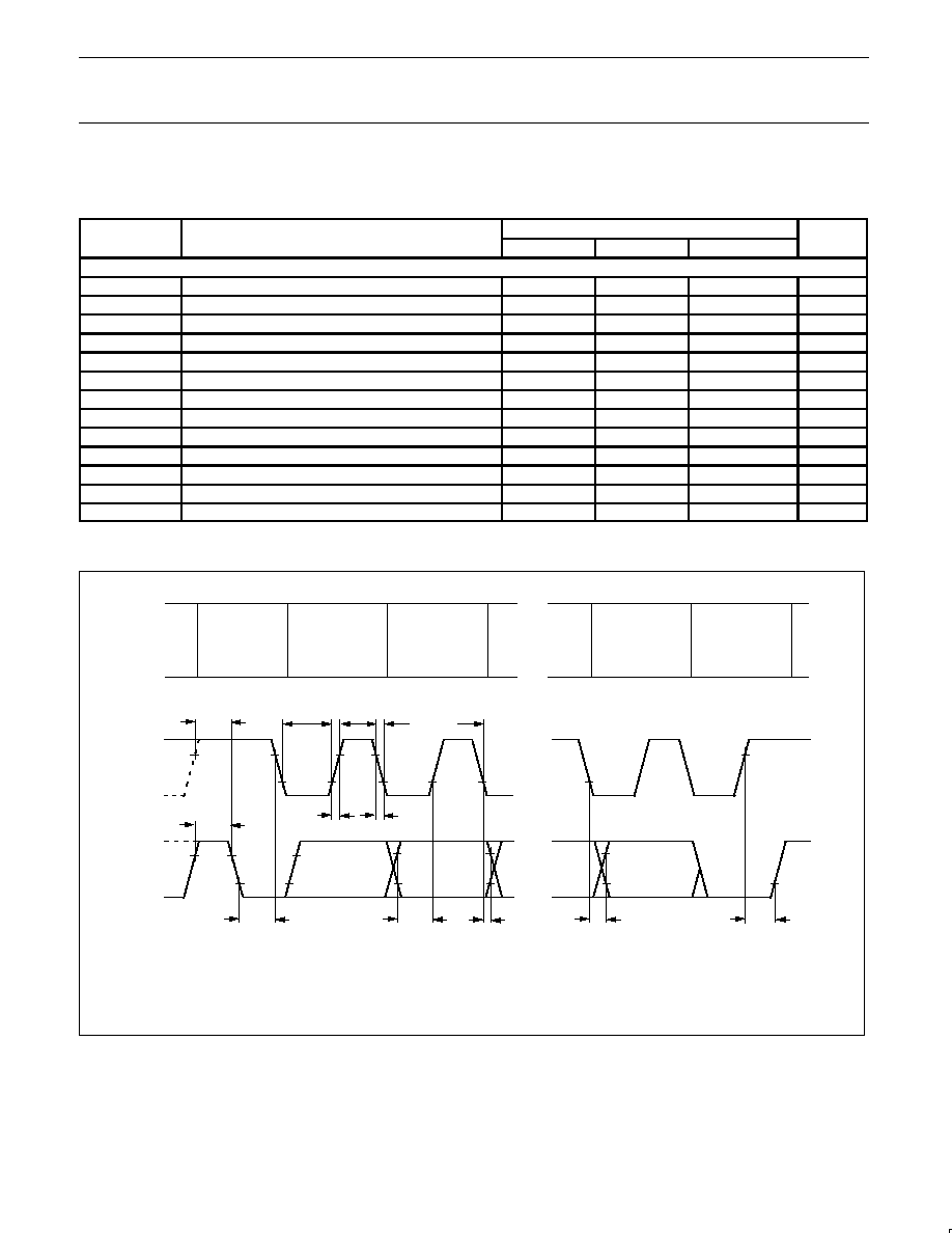
DIFFERENTIAL
DATA LINES
T
PERIOD
CROSSOVER
POINT EXTENDED
CROSSOVER
POINT
SOURCE EOP WIDTH: T
EOPT
RECEIVER EOP WIDTH: T
EOPR1
, T
EOPR2
DIFFERENTIAL DATA TO
SEO/EOP SKEW
N* T
PERIOD
+ T
DEOP
Figure 1. Differential Data to EOP Transition Skew and EOP Width

Philips Semiconductors
Product specification
PDIUSBH11
Universal Serial Bus Hub
1997 Aug 01
21
CROSSOVER
POINT
CROSSOVER
POINT
CROSSOVER
POINT
SV00514
CROSSOVER
POINT
Hub Delay
Downstream
T
HDD
Hub Delay
Upstream
T
HDD
DOWNSTREAM
DIFFERENTIAL
DATA
UPSTREAM-
DIFFERENTIAL
DATA
UPSTREAM
DIFFERENTIAL
DATA
DOWNSTREAM-
DIFFERENTIAL
DATA
V
DD
V
SS
V
SS
A. DOWNSTREAM HUB DELAY
B. UPSTREAM HUB DELAY
SOP DISTORTION
T
SOP
= T
HDD
(SOP) T
HDD
(NEXT J)
LOW SPEED TIMINGS ARE DETERMINED IN THE SAME WAY FOR:
T
LHDD
AND T
LSOP
Figure 2. Hub Differential Data Delay and SOP Distortion
UPSTREAM-
DIFFERENTIAL
DATA
DOWNSTREAM-
DIFFERENTIAL
DATA
V
DD
V
SS
V
SS
A. DOWNSTREAM EOP DELAY
B. UPSTREAM EOP DELAY
EOP DELAY
T
EOPD
= T
EOP
EOP DELAY RELATIVE TO T
HDD
T
EOPDR
= T
EOPD
T
HDD
EOP SKEW
T
HESK
= T
EOP+
T
EOP
LOW SPEED TIMINGS ARE DETERMINED IN THE SAME WAY FOR:
T
LEOPD
, T
LEOPDR
, AND T
LHESK
T
EOP+
T
EOP
CROSSOVER
POINT
EXTENDED
CROSSOVER
POINT
EXTENDED
UPSTREAM
END OF CABLE
DOWNSTREAM
PORT
T
EOP+
T
EOP
CROSSOVER
POINT
EXTENDED
CROSSOVER
POINT
EXTENDED
SV00515
Figure 3. Hub EOP Delay and EOP Skew
Philips Semiconductors
Product specification
PDIUSBH11
Universal Serial Bus Hub
1997 Aug 01
22
AC CHARACTERISTICS (I
2
C)
All timing values are valid within the operating supply voltage and ambient temperature range and reference to V
IL
and V
IH
with an input voltage
swing of V
SS
and V
DD
.
SYMBOL
PARAMETER
LIMITS
UNIT
SYMBOL
PARAMETER
MIN
TYP
MAX
UNIT
I
2
C-bus timing (see Figure ; Note )
f
SCL
SCL clock frequency
100
kHZ
t
SP
Tolerable spike width on bus
100
ns
t
BUF
Bus free time
4.7
µ
s
t
SU;STA
Start condition set-up time
4.7
µ
s
t
HD;STA
Start condition hold time
4.0
µ
s
t
LOW
SCL LOW time
4.7
µ
s
t
HIGH
SCL HIGH time
4.0
µ
s
t
r
SCL and SDA rise times
1.0
µ
s
t
f
SCL and SDA fall times
0.3
µ
s
t
SU;DAT
Data set-up time
250
ns
t
HD;DAT
Data hold time
0
ns
t
VD;DAT
SCL LOW to data out valid
3.4
µ
s
t
SU;STO
Stop condition set-up time
4.0
µ
s
1. A detailed description of the I
2
C-bus specification, with applications, is given in brochure ``
The I
2
C-bus and how to use it". This brochure
may be ordered using the code 9398 393 40011.
SV00756
SCL
SDA
PROTOCOL
t
SU;STA
t
LOW
t
HIGH
1/f
SCL
t
BUF
t
r
t
f
t
HD;STA
t
SU;DAT
t
HD;DAT
t
VD:DAT
t
SU;STO
BIT 0
LSB
(R/W)
ACKNOWLEDGE
(A)
STOP
CONDITION
(P)
START
CONDITION
(S)
BIT 7
MSB
(A7)
BIT 6
(A6)
Figure 4. I
2
C-bus timing diagram; rise and fall times refer to V
IL
and V
IH

Philips Semiconductors
Product specification
PDIUSBH11
Universal Serial Bus Hub
1997 Aug 01
23
SO32:
plastic small outline package; 32 leads; body width 7.5mm
SOT287-1
Philips Semiconductors
Product specification
PDIUSBH11
Universal Serial Bus Hub
1997 Aug 01
24
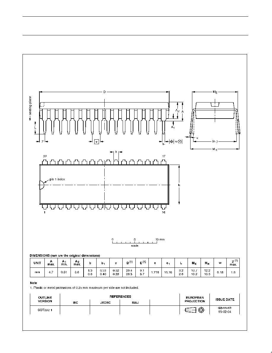
SDIP32:
plastic shrink dual in-line package; 32 leads (400 mil)
SOT232-1

Philips Semiconductors
Product specification
PDIUSBH11
Universal Serial Bus Hub
1997 Aug 01
25
NOTES

Philips Semiconductors
Product specification
PDIUSBH11
Universal serial bus hub
1997 Apr 17
26
Philips Semiconductors and Philips Electronics North America Corporation reserve the right to make changes, without notice, in the products,
including circuits, standard cells, and/or software, described or contained herein in order to improve design and/or performance. Philips
Semiconductors assumes no responsibility or liability for the use of any of these products, conveys no license or title under any patent, copyright,
or mask work right to these products, and makes no representations or warranties that these products are free from patent, copyright, or mask
work right infringement, unless otherwise specified. Applications that are described herein for any of these products are for illustrative purposes
only. Philips Semiconductors makes no representation or warranty that such applications will be suitable for the specified use without further testing
or modification.
LIFE SUPPORT APPLICATIONS
Philips Semiconductors and Philips Electronics North America Corporation Products are not designed for use in life support appliances, devices,
or systems where malfunction of a Philips Semiconductors and Philips Electronics North America Corporation Product can reasonably be expected
to result in a personal injury. Philips Semiconductors and Philips Electronics North America Corporation customers using or selling Philips
Semiconductors and Philips Electronics North America Corporation Products for use in such applications do so at their own risk and agree to fully
indemnify Philips Semiconductors and Philips Electronics North America Corporation for any damages resulting from such improper use or sale.
This data sheet contains preliminary data, and supplementary data will be published at a later date. Philips
Semiconductors reserves the right to make changes at any time without notice in order to improve design
and supply the best possible product.
Philips Semiconductors
811 East Arques Avenue
P.O. Box 3409
Sunnyvale, California 940883409
Telephone 800-234-7381
DEFINITIONS
Data Sheet Identification
Product Status
Definition
Objective Specification
Preliminary Specification
Product Specification
Formative or in Design
Preproduction Product
Full Production
This data sheet contains the design target or goal specifications for product development. Specifications
may change in any manner without notice.
This data sheet contains Final Specifications. Philips Semiconductors reserves the right to make changes
at any time without notice, in order to improve design and supply the best possible product.
©
Copyright Philips Electronics North America Corporation 1997
All rights reserved. Printed in U.S.A.
Philips
Semiconductors