
Philips
Semiconductors
PDI1394L21
1394 full duplex AV link layer controller
Preliminary specification
Supersedes data of 1999 Mar 30
1999 Aug 06
INTEGRATED CIRCUITS
NOTICE:
SEE ATTACHED ERRATA WHICH FOLLOWS THIS DOCUMENT FOR INFORMATION
REGARDING CHANGED SPECIFICATIONS
Philips Semiconductors
Preliminary specification
PDI1394L21
1394 full duplex AV link layer controller
2
1999 Aug 06
1.0
FEATURES
·
IEEE 13941995 Standard Link Layer Controller
·
Hardware Support for the IEC61883 International Standard of
Digital Interface for Consumer Electronics
·
Interface to any IEEE 13941995 Physical Layer Interface
·
5V Tolerant I/Os
·
Single 3.3V supply voltage
·
Full-duplex isochronous operation
·
Operates with 400/200/100 Mbps physical layer devices
·
Dual 4K Byte FIFOs for isochronous data
·
Supports single capacitor isolation mode and IEEE 13941995,
Annex J. isolation
·
4-field deep SYT buffer added to enhance real-time isochronous
synchronization using the AVFSYNC pin
·
Generates its own AV port clocks under software control. Select
one of three frequencies: 24.576, 12.288, or 6.144 MHz
2.0
DESCRIPTION
The PDI1394L21, Philips Semiconductors Full Duplex 1394
Audio/Video (AV) Link Layer Controller, is an IEEE 13941995
compliant link layer controller featuring 2 embedded AV layer
interfaces. The AV layers are designed to pack and un-pack
application data packets for transmission over the IEEE 1394 bus
using isochronous data transfers. Because of its full duplex
architecture, the PDI1394L21 is capable of receiving and
transmitting isochronous data during the same bus cycle. Two 8 bit
AV ports, each with its own buffer (FIFO), receive and output
isochronous data for transmission and reception of bus packets.
Each port can be configured to receive or transmit, however, the
other port always performs the opposite function. Half duplex
operation is also permitted.
The application data is packetized according to the IEC 61883
International Standard of Interface for Consumer Electronic
Audio/Video Equipment. Both AV layer interfaces are byte-wide
ports capable of accommodating various MPEG2 and DVC
codecs. An 80C51 compatible byte-wide host interface is provided
for internal register configuration as well as performing
asynchronous data transfers.
The PDI1394L21 is powered by a single 3.3V power supply and the
inputs and outputs are 5V tolerant. It is available in the LQFP100
and TQFP100 packages.
3.0
QUICK REFERENCE DATA
GND = 0V; T
amb
= 25
°
C
SYMBOL
PARAMETER
CONDITIONS
MIN
TYP
MAX
UNIT
V
DD
Functional supply voltage range
3.0
3.3
3.6
V
I
DD
Supply current @ V
DD
= 3.3V
Operating
75
mA
SCLK
Device clock
49.147
49.152
49.157
MHz
4.0
ORDERING INFORMATION
PACKAGES
TEMPERATURE RANGE
OUTSIDE NORTH AMERICA
NORTH AMERICA
PKG. DWG. #
100-pin plastic LQFP100
0
°
C to +70
°
C
PDI1394L21BE
PDI1394L21BE
SOT407 AB15
100-pin plastic TQFP100
0
°
C to +70
°
C
PDI1394L21BP
PDI1394L21BP
SOT386 BB2
NOTE:
This datasheet is subject to change.
Please visit out internet website www.semiconductors.philips.com/1394 for latest changes.

Philips Semiconductors
Preliminary specification
PDI1394L21
1394 full duplex AV link layer controller
1999 Aug 06
3
5.0
PIN CONFIGURATION
Pin
Function
1
HIF D7
2
HIF D6
3
HIF D5
4
HIF D4
5
GND
6
V
DD
7
HIF D3
8
HIF D2
9
HIF D1
10
HIF D0
11
CLK25
12
GND
13
V
DD
14
HIF A8
15
HIF A7
16
HIF A6
17
HIF A5
18
HIF A4
19
HIF A3
20
HIF A2
21
HIF A1
22
HIF A0
23
GND
24
V
DD
25
HIF CS_N
26
HIF WR_N
27
HIF RD_N
28
HIF INT_N
29
RESET_N
30
CYCLE IN
31
GND
32
V
DD
33
CYCLE OUT
34
PHY D7*
Pin
Function
35
PHY D6*
36
PHY D5*
37
PHY D4*
38
GND
39
V
DD
40
PHY D3*
41
PHY D2*
42
PHY D1*
43
PHY D0*
44
GND
45
V
DD
46
PHY CTL1*
47
PHY CTL0*
48
ISO_N
49
V
DD
50
GND
51
N/C
52
AV1ERR1
53
AV1ERR0
54
LREQ*
55
SCLK
56
AV1ENDPCK
57
AV1SYNC
58
AV1CLK
59
AV1FSYNC
60
AV1ENKEY
61
AV1VALID
62
N/C
63
GND
64
V
DD
65
RESESRVED
66
RESERVED
67
RESERVED
68
AV1 D0
Pin
Function
69
AV1 D1
70
AV1 D2
71
AV1 D3
72
V
DD
73
GND
74
AV1 D4
75
AV1 D5
76
AV1 D6
77
AV1 D7
78
V
DD
79
GND
80
AV2ERR1
81
AV2ERR0
82
AV2ENDPCK
83
AV2SYNC
84
AV2CLK
85
AV2FSYNC
86
AV2VALID
87
GND
88
V
DD
89
AV2 D0
90
AV2 D1
91
AV2 D2
92
AV2 D3
93
GND
94
V
DD
95
AV2D4
96
AV2 D5
97
AV2 D6
98
AV2 D7
99
AV2ENKEY
100
N/C
* INDICATES PIN EQUIPPED WITH INTERNAL BUS HOLD CIRCUIT
ACTIVATED BY THE STATE OF THE ISO_N PIN.
TQFP
LQFP
100
76
1
25
75
51
26
50
SV00877

Philips Semiconductors
Preliminary specification
PDI1394L21
1394 full duplex AV link layer controller
1999 Aug 06
4
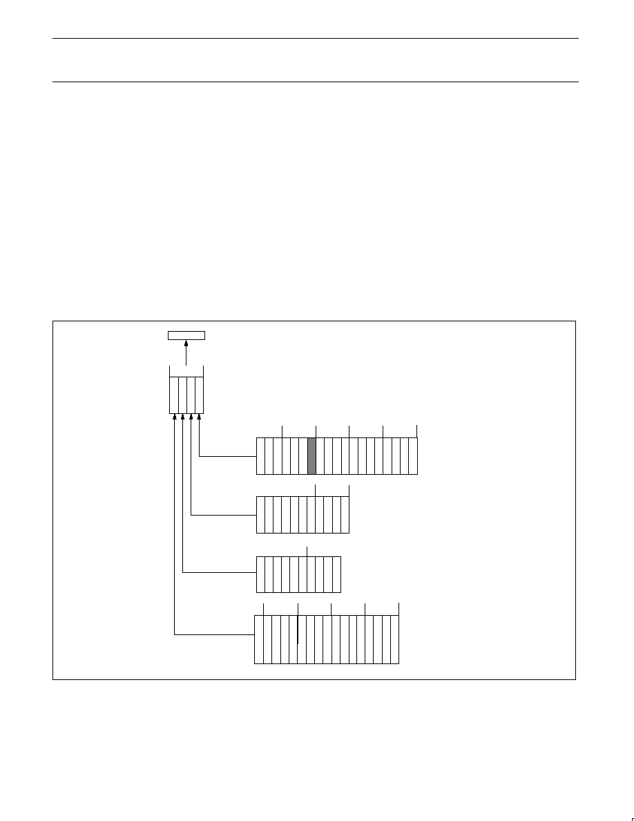
6.0
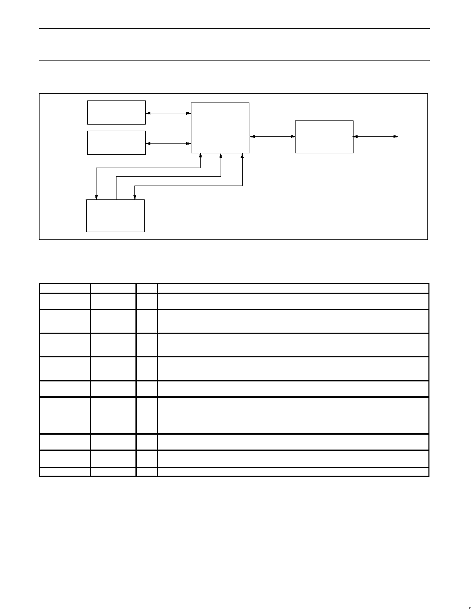
FUNCTIONAL DIAGRAM
A
V
LA
YER
1
HOST
PHY
HIF A[8:0]
HIF D[7:0]
HIF WR_N
HIF RD_N
HIF CS_N
HIF INT_N
RESET_N
CYCLEIN
CYCLEOUT
AV1 D[7:0]
AV1CLK
AV1SYNC
AV1FSYNC
AV2FSYNC
AV1ENDPCK
AV1ERR[1:0]
PHY D[0:7]
PHY CTL[0:1]
LREQ
ISO_N
SCLK
VDD
GND
PDI1394L21
IEEE 1394
FULL DUPLEX
AV LINK LAYER CONTROLLER
AV1VALID
SV00878
A
V
LA
YER
2
AV2D[7:0]
AV2CLK
AV2VALID
AV2SYNC
AV2ENDPCK
AV2ERR[1:0]
AV1ENKEY
AV2ENKEY
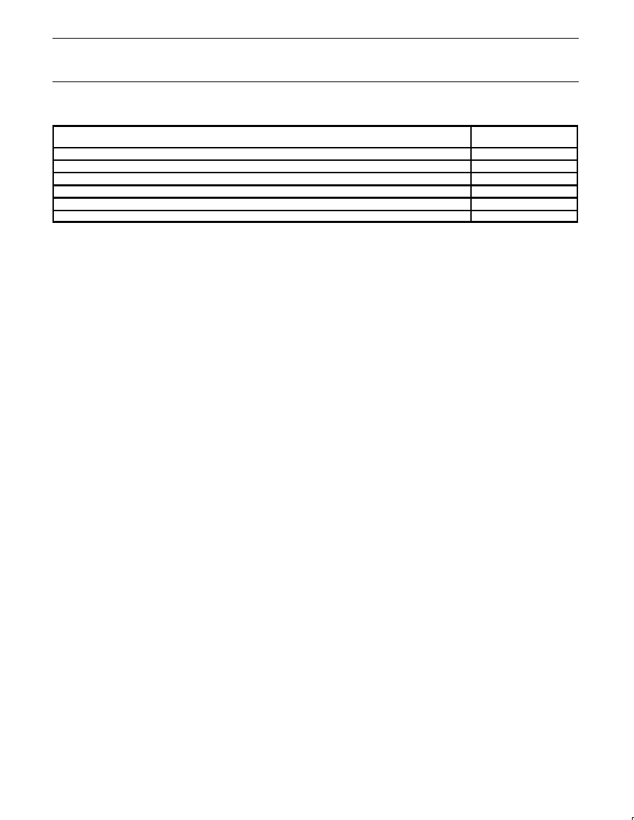
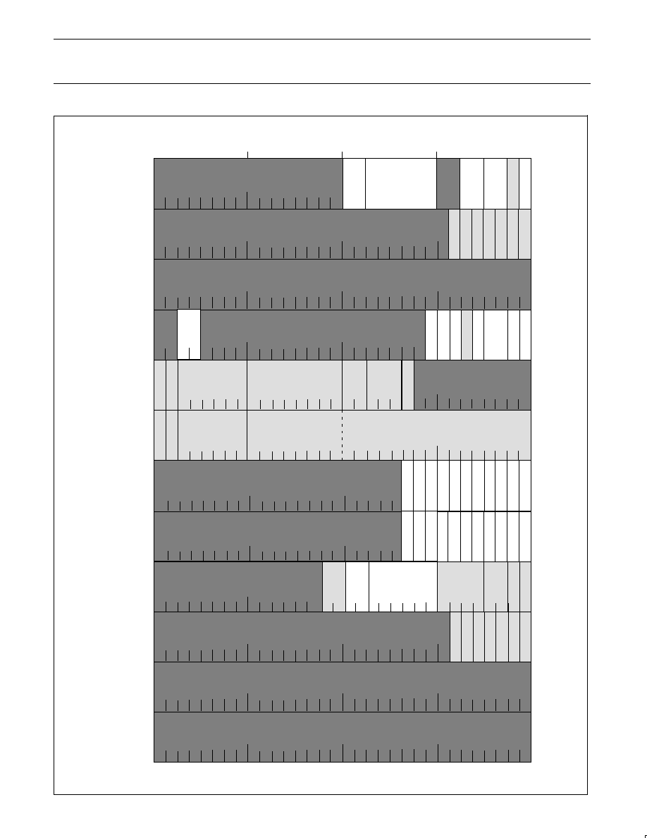
7.0
INTERNAL BLOCK DIAGRAM
HIF A[8:0]
HIF D[7:0]
HIF WR_N
HIF RD_N
HIF CS_N
HIF INT_N
RESET_N
CYCLEIN
CYCLEOUT
AV1 D[7:0]
AV1CLK
AV1SYNC
AV1FSYNC
AV1ENDPCK
AV1ERR[0:1]
PHY D[0:7]
PHY CTL[0:1]
LREQ
ISO_N
SCLK
AV1VALID
AV1 LAYER
ISOCHRONOUS
TRANSMITTER/
RECEIVER
9KB BUFFER
MEMORY
(ISOCH & ASYNC
PACKETS)
LINK CORE
8-BIT
INTERFACE
ASYNC
TRANSMITTER
AND
RECEIVER
CONTROL
AND
STATUS
REGISTERS
AV2 D[7:0]
AV2CLK
AV2SYNC
AV2FSYNC
AV2ENDPCK
AV2VALID
AV2 LAYER
ISOCHRONOUS
TRANSMITTER/
RECEIVER
A
V
LA
YER2
A
V
LA
YER1
AV2ERR[0:1]
SV00879
AV1ENKEY
AV2ENKEY
NOTE: THERE IS ONLY ONE
ISOCHRONOUS RECEIVER
AND ONE ISOCHRONOUS
TRANSMITTER--THEREFORE,
WHEN EITHER AVPORT IS SET
TO TRANSMIT, THE OTHER
AVPORT IS AUTOMATICALLY
SET TO RECEIVE.
Philips Semiconductors
Preliminary specification
PDI1394L21
1394 full duplex AV link layer controller
1999 Aug 06
5
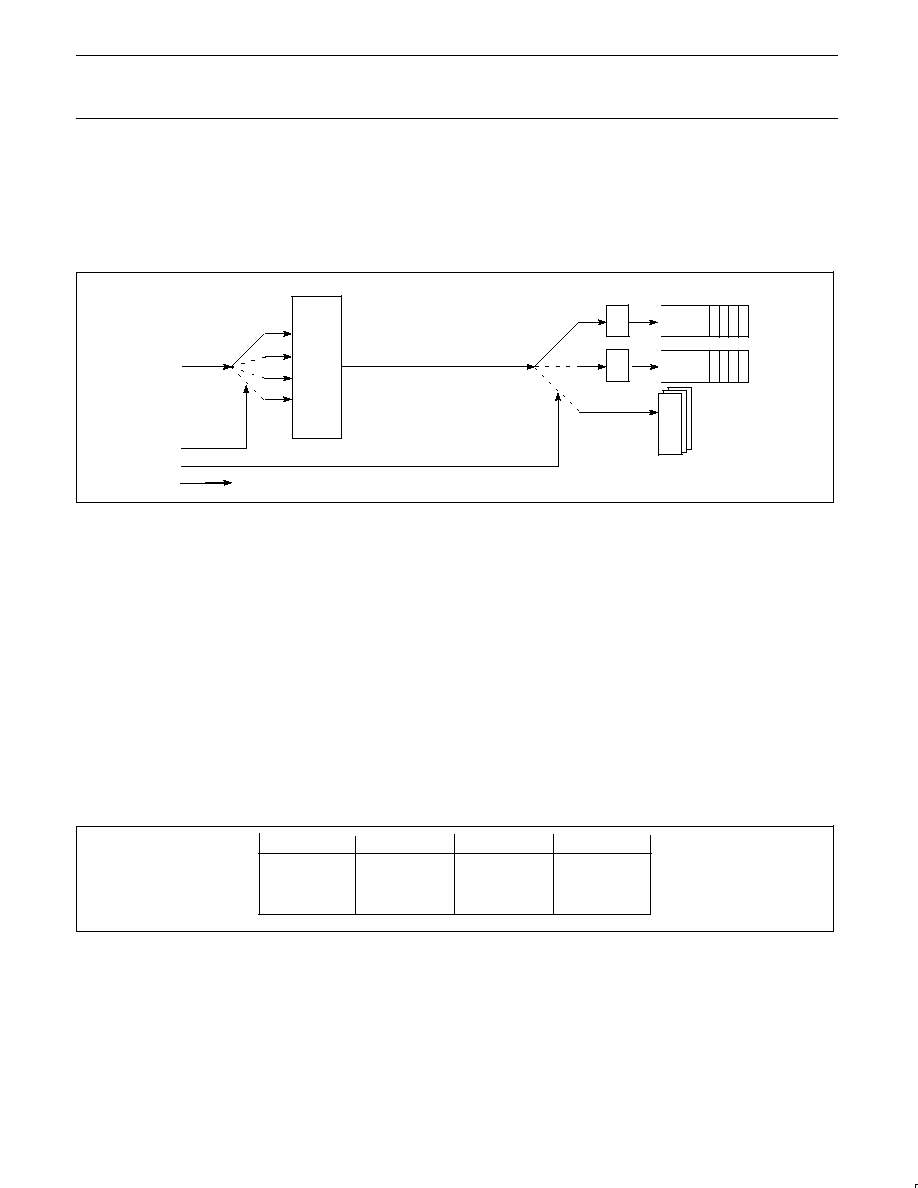
8.0
APPLICATION DIAGRAM
MPEG OR DVC
DECODER
PDI1394L21
AV LINK
AV
INTERFACE
PDI1394Pxx
PHY
PHYLINK
INTERFACE
HOST CONTROLLER
DATA 8/
ADDRESS 9/
INTERRUPT & CONTROL
1394 CABLE
INTERFACE
MPEG OR DVC
DECODER
AV
INTERFACE
SV00880
9.0
PIN DESCRIPTION
9.1
Host Interface
PIN No.
PIN SYMBOL
I/O
NAME AND FUNCTION
1, 2, 3, 4, 7, 8,
9, 10
HIF D[7:0]
I/O
Host Interface Data 7 (MSB) through 0. Byte wide data path to internal registers.
5, 12, 23, 31,
38, 44, 50, 63,
73, 79, 87, 93
GND
Ground reference
6, 13, 24, 32,
39, 45, 49, 64,
72, 78, 88, 94
V
DD
3.3V
±
0.3V power supply
14, 15, 16, 17,
18, 19, 20, 21,
22
HIF A[8:0]
I
Host Interface Address 0 through 8. Provides the host with a byte wide interface to internal
registers. See description of Host Interface for addressing rules.
25
HIF CS_N
I
Chip Select (active LOW). Host bus control signal to enable access to the FIFO and control and
status registers.
26
HIF WR_N
I
Write enable. When asserted (LOW) in conjunction with HIF CS_N, a write to the PDI1394L21
internal registers is requested. (NOTE: HIF WR_N and HIF RD_N : if these are both LOW in
conjunction with HIF CS_N, then a write cycle takes place. This can be used to connect CPUs
that use R/W_N line rather than separate RD_N and WR_N lines. In that case, connect the
R/W_N line to the HIF WR_N and tie HIF RD_N LOW.)
27
HIF RD_N
I
Read enable. When asserted (LOW) in conjunction with HIF CS_N, a read of the PDI1394L21
internal registers is requested.
28
HIF INT_N
O
Interrupt (active LOW). Indicates a interrupt internal to the PDI1394L21. Read the General
Interrupt Register for more information. This pin is open drain and requires a 1K
W
pull-up resistor.
29
RESET_N
I
Reset (active LOW). The asynchronous master reset to the PDI1394L21.

Philips Semiconductors
Preliminary specification
PDI1394L21
1394 full duplex AV link layer controller
1999 Aug 06
6
9.2
AV Interface 1
NOTE: This AV interface may be configured to transmit or receive according to the condition of "DIRAV1" bit in GLOBCSR register
(0X018)--default is transmit.
PIN No.
PIN SYMBOL
I/O
NAME AND FUNCTION
77, 76, 75, 74,
71, 70, 69, 68
AV1 D[7:0]
I/O
Audio/Video Data 7 (MSB) through 0. Byte-wide interface to the AV layer 1.
58
AV1CLK
I/O
External application clock. Rising edge active. This pin can be programmed to output the
application clock. Depending on the configuration of AV Port 1 as transmitter or receiver, the
output enable is located in the ITXPKCTL register (address 0x020) or IRXPKCTL register
(address 0x040).
57
AV1SYNC
I/O
Start of packet indicator; should only be used when AV1VALID is active.
59
AV1FSYNC
I/O
Programmable frame sync, can be set to input. Frame sync input used for Digital Video (DV). The
signal is time stamped and transmitted in the SYT field of ITXHQ2. Frame sync output. Signal is
derived from SYT field of IRXHQ2.
56
AV1ENDPCK
I
End of application packet indication from data source. Required only if input packet is not multiple
of 4 bytes. It can be tied LOW for data packets that are 4*N in size.
60
AV1ENKEY
I/O
Encryption key state. Indicates state "1" or "0" of encryption key which matches present port data
during receive mode. Used to input key state during transmit mode.
61
AV1VALID
I/O
Indicates data on AV1 D [7:0] is valid.
53
AV1ERR0
O
CRC error, indicates bus packet containing AV1 D [7:0] had a CRC error, the current AV packet is
unreliable.
52
AV1ERR1
O
Sequence Error. Indicates at least one source packet was lost before the current AV1 D [7:0] data.
9.3
AV Interface 2
NOTE: This AV interface may be configured to transmit or receive according to the condition of "DIRAV1" bit in GLOBCSR register--default is
receive.
PIN No.
PIN SYMBOL
I/O
NAME AND FUNCTION
98, 97, 96, 95,
92, 91, 90, 89
AV2 D[7:0]
I/O
Audio/Video Data 7 (MSB) through 0. Byte-wide interface to the AV layer 2.
84
AV2CLK
I/O
External application clock. Rising edge active. This pin can be programmed to output the
application clock. Depending on the configuration of AV Port 2 as transmitter or receiver, the
output enable is located in the ITXPKCTL register (address 0x020) or IRXPKCTL register
(address 0x040).
83
AV2SYNC
I/O
Start of packet indicator; should only be used when AV2VALID is active.
85
AV2FSYNC
I/O
Programmable frame sync, can be set to input or output. Frame sync input used for Digital Video
(DV). The signal is time stamped and transmitted in the SYT field of ITXHQ2. Frame sync output.
Signal is derived from SYT field of IRXHQ2.
82
AV2ENDPCK
I
End of application packet indication from data source. Required only if input packet is not multiple
of 4 bytes. It can be tied LOW for data packets that are 4*N in size.
86
AV2VALID
I/O
Indicates data on AV2 D [7:0] is valid.
81
AV2ERR0
O
CRC error, indicates bus packet containing AV2 D [7:0] had a CRC error, the current AV packet is
unreliable.
80
AV2ERR1
O
Sequence Error. Indicates at least one source packet was lost before the current AV2 D [7:0] data.
99
AV2ENKEY
I/O
Encryption key state. Indicates state "1" or "0" of encryption key which matches present port data
during receive mode. Used to input key state during transmit mode.
9.4
Phy Interface
PIN No.
PIN SYMBOL
I/O
NAME AND FUNCTION
43, 42, 41, 40,
37, 36, 35, 34
PHY D[0:7]
I/O
Data 0 (MSB) through 7 (NOTE: To preserve compatibility to the specified Link-Phy interface of
the IEEE 13941995 standard, Annex J, bit 0 is the most significant bit). Data is expected on
PHY D[0:1] for 100Mb/s, PHY D[0:3] for 200Mb/s, and PHY D[0:7] for 400Mb/s. See IEEE
13941995 standard, Annex J for more information.
47, 46
PHY CTL[0:1]
I/O
Control Lines between Link and Phy. See 1394 Specification for more information.
48
ISO_N
I
Isolation mode. This pin is asserted (LOW) when an Annex J type isolation barrier is used.
See IEEE 13941995 Annex J. for more information. When tied HIGH, this pin enables internal
bushold circuitry on the affected PHY interface pins (see below). Active bushold circuits allow
either the direct connection to PHY pins or the use of the single capacitor isolation mode.
54
LREQ
O
Link Request. Bus request to access the PHY. See IEEE 13941995 standard, Annex J for more
information. (Used to request arbitration or read/write PHY registers).
55
SCLK
I
System clock. 49.152MHz input from the PHY (the PHY-LINK interface operates at this frequency).

Philips Semiconductors
Preliminary specification
PDI1394L21
1394 full duplex AV link layer controller
1999 Aug 06
7
9.4.1
Bushold and Link/PHY single capacitor
galvanic isolation
9.4.1.1
Bushold
The PDI1394L21 uses an internal bushold circuit on each of the
indicated pins to keep these CMOS inputs from "floating" while being
driven by a 3-Stated device or input coupling capacitor.
Unterminated high impedance inputs react to ambient electrical
noise which cause internal oscillation and excess power supply
current draw.
The following pins have bushold circuitry enabled when the ISO_N
pin is in the logic "1" state:
Pin No.
Name
Function
47
PHYCTL0
PHY control line 0
46
PHYCTL1
PHY control line 1
54
LREQ
Link request line
43
PHYD0
PHY data bus bit 0
42
PHYD1
PHY data bus bit 1
41
PHYD2
PHY data bus bit 2
40
PHYD3
PHY data bus bit 3
37
PHYD4
PHY data bus bit 4
36
PHYD5
PHY data bus bit 5
35
PHYD6
PHY data bus bit 6
34
PHYD7
PHY data bus bit 7
Philips bushold circuitry is designed to provide a high resistance
pull-up or pull-down on the input pin. This high resistance is easily
overcome by the driving device when its state is switched. Figure 1
shows a typical bushold circuit applied to a CMOS input stage. Two
weak MOS transistors are connected to the input. An inverter is also
connected to the input pin and supplies gate drive to both
transistors. When the input is LOW, the inverter output drives the
lower MOS transistor and turns it on. This re-enforces the LOW on
the input pin. If the logic device which normally drives the input pin
were to be 3-Stated, the input pin would remain "pulled-down" by the
weak MOS transistor. If the driving logic device drives the input pin
HIGH, the inverter will turn the upper MOS transistor on,
re-enforcing the HIGH on the input pin. If the driving logic device is
then 3-Stated, the upper MOS transistor will weakly hold the input
pin HIGH.
The PHY's outputs can be 3-Stated and single capacitor isolation
can be used with the Link; both situations will allow the Link inputs to
float. With bushold circuitry enabled, these pins are provided with dc
paths to ground, and power by means of the bushold transistors;
this arrangement keeps the inputs in known logical states.
SV00911
INPUT PIN
INTERNAL
CIRCUITS
Figure 1. Bushold circuit
9.4.1.2
Single capacitor isolation
The circuit example (Figure 2) shows the connections required to
implement basic single capacitor Link/PHY isolation.
NOTE: The isolation enablement pins on both devices are in their
"1" states, activating the bushold circuits on each part. The bushold
circuits provide local dc ground references to each side of the
isolating/coupling capacitors. Also note that ground
isolation/signal-coupling must be provided in the form of a parallel
combination of resistance and capacitance as indicated in
IEEE 13941995.
D0
D1
D2
D3
PHYCTL0
PHYCTL1
LREQ
SYSCLK
ISO
Cc
PHY
PDI1394Pxx
ISOLATED PHY GROUND
Cc
Cc
Cr
Cc
Cc
Cc
1MEG
Cc
Cc
PHY D0
PHY D1
PHY D2
PHY D3
PHYCTL0
PHYCTL1
LREQ
SCLK
ISO_N
LINK
PDI1394L21
43
42
41
40
47
46
54
55
48
APPLICATION GROUND
APPLICATION
+3.3V
ISOLATED
+3.3V
SV00912
Cc = 0.001
µ
F; Cr = 0.1
µ
F
6, 13, 24, 32, etc.
Figure 2. Single capacitor Link/PHY isolation

Philips Semiconductors
Preliminary specification
PDI1394L21
1394 full duplex AV link layer controller
1999 Aug 06
8
9.5
Other Pins
PIN No.
PIN SYMBOL
I/O
NAME AND FUNCTION
65, 66, 67
RESERVED
NA
These pins are reserved for factory testing. For normal operation they should be connected to
ground.
51, 62, 100
N/C
NA
These pins should not be connected or terminated.
30
CYCLEIN
I
Provides the capability to supply an external cycle timer signal for the beginning of 1394 bus
cycles.
33
CYCLEOUT
O
Reproduces the 8kHz cycle clock of the cycle master.
11
CLK25
O
Auxiliary clock, value is SCLK/2 (usually 24.576 MHz)
10.0
RECOMMENDED OPERATING CONDITIONS
SYMBOL
PARAMETER
CONDITIONS
LIMITS
UNIT
SYMBOL
PARAMETER
CONDITIONS
MIN.
MAX.
UNIT
V
CC
DC supply voltage
3.0
3.6
V
V
I
Input voltage
0
5
V
V
IH
High-level input voltage
2.0
V
V
IL
Low-level input voltage
0.8
V
I
OH
High-level output current
8
mA
I
OL
Low-level output current
8
mA
dT/dV
Input transition rise or fall time
0
20
ns/V
T
amb
Operating ambient temperature range
0
+70
°
C
SCLK
System clock
49.147
49.157
MHz
AVCLK
AV interface clock
0
24
MHz
t
r
Input rise time
10
ns
t
f
input fall time
10
ns
11.0
ABSOLUTE MAXIMUM RATINGS
1, 2
In accordance with the Absolute Maximum Rating System (IEC 134). Voltages are referenced to GND (ground = 0V).
SYMBOL
PARAMETER
CONDITIONS
LIMITS
UNIT
SYMBOL
PARAMETER
CONDITIONS
MIN
MAX
UNIT
V
DD
DC supply voltage
0.5
+4.6
V
I
IK
DC input diode current
50
mA
V
I
DC input voltage
0.5
+5.5
V
I
OK
DC output diode current
±
50
mA
V
O
DC output voltage
0.5
V
DD
+0.5
V
I
O
DC output source or sink current
±
50
mA
I
GND
, I
CC
DC V
CC
or GND current
±
150
mA
T
stg
Storage temperature range
60
150
°
C
T
amb
Operating ambient temperature
0
70
°
C
P
tot
Power dissipation per package
0.6
W
NOTES:
1. Stresses beyond those listed may cause permanent damage to the device. These are stress ratings only and functional operation of the
device at these or any other conditions beyond those indicated under "recommended operating conditions" is not implied. Exposure to
absolute-maximum-rated conditions for extended periods may affect device reliability.
2. The performance capability of a high-performance integrated circuit in conjunction with its thermal environment can create junction
temperatures which are detrimental to reliability. The maximum junction temperature of this integrated circuit should not exceed 150
°
C.
Philips Semiconductors
Preliminary specification
PDI1394L21
1394 full duplex AV link layer controller
1999 Aug 06
9
11.1
Buffer Memory Sizes
BUFFER MEMORY
SIZE
(Quadlets)
Asynchronous Receive Response FIFO
64
Asynchronous Receive Request FIFO
128
Asynchronous Transmit Response FIFO
64
Asynchronous Transmit Request FIFO
64
Isochronous (AV) Transmit Buffer
1024
Isochronous (AV) Receive Buffer
1024
12.0
FUNCTIONAL DESCRIPTION
12.1
Overview
The PDI1394L21 is an IEEE 13941995 compliant link layer controller. It provides a direct interface between a 1394 bus and various MPEG2
and DVC codecs. Via this interface, the AV Link maps and unmaps these AV datastreams from these codecs onto 1394 isochronous bus
packets. The AV Link also provides an 8051 compatible microcontroller interface for an attached host controller. Through the host interface port,
the host controller can configure the AV layer for transmission or reception of AV datastreams. The host interface port also allows the host
controller to transmit and receive 1394 asynchronous data packets.
12.2
AV interface and AV layer
The AV interface and AV layer allow AV packets to be transmitted from one node to another. The AV transmitter and receiver within the AV layer
perform all the functions required to pack and unpack AV packet data for transfer over a 1394 network. Once the AV layer is properly configured
for operation, no further host controller service should be required. The operation of the AV layer is full-duplex, i.e., the AV layer can receive and
transmit AV packets at the same time.
12.2.1
The AV Interface
The AV Link provides an 8 bit data path to the AV layer. The 8 bit data path is designed with associated clock and control signals to be
compatible with various MPEG2 and DVC codecs.
The AV interface port buffer, if so programmed, can time stamp incoming AV packets. The AV packet data is stored in the embedded memory
buffer, along with its time stamp information. After the AV packet has been written into the AV layer, the AV layer creates an isochronous bus
packet with the appropriate CIP header. The bus packet along with the CIP header is transferred over the appropriate isochronous
channel/packet. The size and configuration of isochronous data packet payload transmitted is determined by the AV layer's configuration
registers accessible through the host interface.
The AV interface port waits for the assertion for AVxVALID and AVxSYNC. Note: Do not assert AVxSYNC without AVxVALID. AVxSYNC is
aligned with the rising edge of AVxCLK and the first byte of data on AVxDATA[7:0]. The duration of AVxSYNC is one AVxCLK cycle. AVxSYNC
signals the AV layer that the transfer of an AV packet has begun. At the time the AVxSYNC is asserted, the AV layer creates a new time stamp
in the buffer memory. (This only happens if so configured. The DVC format does not use these time stamps). The time stamp is then transmitted
as part of the source packet header. This allows the AV receiver to provide the AV packet for output at the appropriate time. Only one AVSYNC
pulse is allowed per application packet; if additional sync pulses are presented before the full packet is inputted, a new packet will be started
and the previously inputted packet data will be discarded (and not transmitted) in conjunction with the input error interrupt bit (INPERR, bit 3 of
register 0x02C) being set to flag the error.
When the DV video is enabled (via the format code of the CIP header), the frame synchronization signal AVxFSYNC is time stamped and
placed in the SYT field. The default timestamp value is 3 cycle times (duration of 125
m
s each) in the future and is transmitted in the SYT field of
the current CIP header; this value is programmable from 2 to 4 cycle times (see section 13.2.1). On the receiver side, when the SYT stamp
matches the cycle timer register, a pulse is generated on the AVxFSYNC output. The timing for AVxFSYNC is independent of AVxCLK.
12.2.2
IEC 61883 International Standard
The PDI1394L21 is specifically designed to support the IEC61883 International Standard of Digital Interface for Consumer Electronic
Audio/Video Equipment. The IEC specification defines a scheme for mapping various types of AV datastreams onto 1394 isochronous data
packets. The standard also defines a software protocol for managing isochronous connections in a 1394 bus called Connection Management
Protocol (CMP). It also provides a framework for transfer of functional commands, called Function Control Protocol (FCP).
12.2.3
CIP Headers
A feature of the IEC61883 International Standard is the definition of Common Isochronous Packet (CIP) headers. These CIP headers contain
information about the source and type of datastream mapped onto the isochronous packets.
The AV Layer supports the use of CIP headers. CIP headers are added to transmitted isochronous data packets at the AV data source. When
receiving isochronous data packets, the AV layer automatically analyzes their CIP headers. The analysis of the CIP headers determines the
method the AV layer uses to unpack the AV data from the isochronous data packets.
The information contained in the CIP headers is accessible via registers in the host interface.
(See IEC61883 International Standard of Digital Interface for Consumer Electronic Audio/Video Equipment for more details on CIP headers).

Philips Semiconductors
Preliminary specification
PDI1394L21
1394 full duplex AV link layer controller
1999 Aug 06
10
12.3
The host interface
The host interface allows an 8 bit CPU to access all registers and the asynchronous packet queues. It is specifically designed for an 8051
microcontroller but can also be used with other CPUs. There are 64 register addresses (for quadlet wide registers). To access bytes rather than
quadlets the address spaces is 256 bytes, requiring 8 address lines.
The use of an 8 bit interface introduces an inherent problem that must be solved: register fields can be more than 8 bits wide and be used
(control) or changed (status) at every internal clock tick. If such a field is accessed through an 8 bit interface it requires more than one read or
write cycle, and the value should not change in between to maintain consistency. To overcome this problem accesses to the chip's internal
register space are always 32 bits, and the host interface must act as a converter between the internal 32 bit accesses and external 8 bit
accesses. This is where the shadow registers are used.
12.3.1
Read accesses
To read an internal register the host interface can make a snapshot (copy) of that specific register which is then made available to the CPU 8
bits at a time. The register that holds the snapshot copy of the real register value inside the host interface is called the read shadow register.
During a read cycle address lines HIF A0 and HIF A1 are used to select which of the 4 bytes currently stored in the read shadow register is
output onto the CPU data bus. This selection is done by combinatorial logic only, enabling external hardware to toggle these lines through
values 0 to 3 while keeping the chip in a read access mode to get all 4 bytes out very fast (in a single extended read cycle), for example into an
external quadlet register.
This solution requires a control line to direct the host interface to make a snapshot of an internal register when needed, as well as the internal
address of the target register. The register address is connected to input address lines HIF A2..HIF A7, and the update control line to input
address line HIF A8. To let the host interface take a new snapshot the target address must be presented on HIF A2..HIF A7 and HIF A8 must be
raised while executing a read access. The new value will be stored in the read shadow register and the selected byte (HIF A0, HIF A1)
appears on the output.
SV00803
UPDATE/COPY CONTROL
HIF A8
HIF A2..7
HIF A0..1
CPU
READ SHADOW REGISTER
8
32
32
32
REGISTERS
TR
Q
Q
MUX
MUX
NOTES:
1. It is not required to read all 4 bytes of a register before reading another register. For example, if only byte 2 of register 0x54 is required a
read of byte address 0x100 + (0
×
54) + 2 = 0x156 is sufficient.
2. The update control line does not necessarily have to be connected to the CPU address line HIF A8. This input could also be controlled by
other means, for example a combinatorial circuit that activates the update control line whenever a read access is done for byte 0. This
makes the internal updating automatic for quadlet reading.
3. Reading the bytes of the read shadow register can be done in any order and as often as needed.
Philips Semiconductors
Preliminary specification
PDI1394L21
1394 full duplex AV link layer controller
1999 Aug 06
11
12.3.2
Write accesses
To write to an internal register the host interface must collect the 4 byte values into a 32 bit value and then write the result to the target register
in a single clock tick. This requires a register to hold the 32 bit value being compiled until it is ready to be written to the actual target register.
This temporary register inside the host interface is called the write shadow register. During all write cycles address lines HIF A0 and HIF A1
are used to select which of the 4 bytes of the write shadow register is to be written with the value on the CPU data bus. Only one byte can be
written in a single write access cycle.
UPDATE/COPY CONTROL
HIF A8
HIF A2..7
HIF A0..1
CPU
WRITE SHADOW REGISTER
8
32
32
REGISTERS
TR
Q
Q
MUX
MUX
SV00804
NOTES:
1. It is not required to write all 4 bytes of a register: those bytes that are either reserved (undefined) or don't care do not have to be written in
which case they will be assigned the value that was left in the corresponding byte of the write shadow register from a previous write
access. For example, to acknowledge an interrupt for the isochronous receiver (external address 0x04C), a single byte write to location
0x100+(0x4C)+3 = 0x14F is sufficient. The value 256 represents setting HIF A8=1. The host interface cannot directly access the FIFOs, but
instead reads from/writes into a transfer register (shown as TR in the Figures above). Data is moved between FIFO and TR by internal logic
as soon as possible without CPU intervention.
2. The update control line does not necessarily have to be connected to the CPU address line HIF A8. This input could also be controlled by
other means, for example a combinatorial circuit that activates the update control line whenever a write access is done for byte 3. This
makes the internal updating automatic for quadlet writing.
3. Writing the bytes of the read shadow register can be done in any order and as often as needed (new writes simply overwrite the old value).
12.3.3
Byte order
The bytes in each quadlet are numbered 0..3 from left (most significant) to right (least significant) as shown in Figure 3. To access a register at
internal address N the CPU should use addresses E:
E = N
; to access the upper 8 bits of the register.
E = N + 1
; to access the upper middle 8 bits of the register.
E = N + 2
; to access the lower middle 8 bits of the register.
E = N + 3
; to access the lower 8 bits of the register.
SV00656
29 28 27 26 25 24 23 22 21 20 19 18 17 16 15 14 13 12 11 10 9 8 7 6 5 4 3 2 1 0
BYTE 0
BYTE 1
BYTE 3
3130
BYTE 2
Figure 3. Byte order in quadlets as implemented in the host interface
12.3.4
Accessing the packet queues
Although entire incoming packets are stored in the receiver buffer memory they are not randomly accessible. These buffers act like FIFOs and
only the frontmost (oldest) data quadlet entry is accessible for reading. Therefore only one location (register address) is allocated to each of the
two receiver queues. Reading this location returns the head entry of the queue, and at the same time removes it from the queue, making the
next stored data quadlet accessible.
With the current host interface such a read is in fact a move operation of the data quadlet from the queue to the read shadow register. Once the
data is copied into the read shadow register it is no longer available in the queue itself so the CPU should always read all 4 bytes before
attempting any other read access (be careful with interrupt handlers for the PDI1394L21!).

Philips Semiconductors
Preliminary specification
PDI1394L21
1394 full duplex AV link layer controller
1999 Aug 06
12
12.3.5
The CPU bus interface signals
The CPU interface is directly compatible with an 8051 microcontroller. It uses a separate HIF RD_N and HIF WR_N inputs and a HIF CS_N chip
select line, all of which are active LOW. There are 9 address inputs (HIF A0..HIF A8) and 8 data in/out lines HIF D0..HIF D7. An open drain
HIF INT_N output is used to signal interrupts to the CPU.
The CPU is not required to run at a clock that is synchronous to the 1394 base clock. The control signals will be resampled by the host interface
before being used internally.
An access through the host interface starts when HIF CS_N = 0 and either HIF WR_N = 0 or HIF RD_N = 0. Typically the chip select signal is
derived from the upper address lines of the CPU (address decode stage), but it could also be connected to a port pin of the CPU to avoid the
need for an external address decoder in very simple CPU systems. When both HIF CS_N = 0 and HIF RD_N = 0 the host interface will start a
read access cycle, so the cycle is triggered at the falling edge of either HIF CS_N or HIF RD_N, whichever is later.
SV00686
TAS
HIF CS_N
HIF RD_N
HIF WR_N
HIF A0..HIF A7
HIF D0..HIF D7
TAS
TACC
TACC
RSRO
RSRn
RSRn
HIF A8
Figure 4. Read cycle signal timing (2 independent read cycles)
SV00687
TAS
HIF CS_N
HIF RD_N
HIF WR_N
HIF A0..HIF A8
HIF D0..HIF D7
TAS
<WRITE DATA>
<WRITE DATA>
<VALID ADDRESS>
<VALID ADDRESS>
Figure 5. Write cycle signal timing (2 independent write cycles)
12.4
The Asynchronous Packet Interface
The PDI1394L21 provides an interface to asynchronous data packets through the registers in the host interface. The format of the
asynchronous packets is specified in the following sections.
12.4.1
Reading an Asynchronous Packet
Upon reception of a packet, the packet data is stored in the appropriate receive FIFO, either the Request or Response FIFO. The location of the
packet is indicated by either the RREQQQAV or RRSPQAV status bit being set in the Asynchronous Interrupt Acknowledge (ASYINTACK)
register. The packet is transferred out of the FIFO by successive reads of the Asynchronous Receive Request (RREQ) or Asynchronous
Receive Response (RRSP) register. The end of the packet (the last quadlet) is indicated by either the RREQQLASTQ or RRSPQLASTQ bit set
in ASYINTACK. Attempting to read the FIFO when either RREQQQAV bit or RRSPQQAV bit is set to 0 (in the Asynchronous RX/TX interrupt
acknowledge (ASYINTACK) register) will result in a queue read error.

Philips Semiconductors
Preliminary specification
PDI1394L21
1394 full duplex AV link layer controller
1999 Aug 06
13
12.5
Link Packet Data Formats
The data formats for transmission and reception of data are shown below. The transmit format describes the expected organization for data
presented to the link at the asynchronous transmit, physical response, or isochronous transmit FIFO interfaces.
12.5.1
Asynchronous Transmit Packet Formats
These sections describe the formats in which packets need to be delivered to the queues (FIFOs) for transmission. There are four basic formats
as follows:
ITEM
FORMAT
USAGE
TRANSACTION CODE
(tCode)
1
No packet data
Quadlet read requests
4
1
No-packet data
Quadlet/block write responses
2
Quadlet write requests
0
2
Quadlet packet
Quadlet read responses
6
Block read requests
5
Block write requests
1
3
Block Packet
Block read responses
7
3
Block Packet
Lock requests
9
Lock responses
B
hex
4
Unformatted transmit
Concatenated self-ID / PHY packets
E
hex
Each packet format uses several fields (see names and descriptions below). More information about these fields (not the format) can be found
in the 1394 specification. Grey fields are reserved and should be set to zero values.
12.5.1.1
No-data Transmit
The no-data transmit formats are shown in Figures 6 and 7. The first quadlet contains packet control information. The second and third quadlets
contain 16-bit destination ID and either the 48-bit, quadlet aligned destination offset (for requests) or the response code (for responses).
destinationID
spd
tLabel
rt
tCode
0000
29 28 27 26 25 24 23 22 21 20 19 18 17 16 15 14 13 12 11 10 9 8 7 6 5 4 3 2 1 0
destinationOffsetHigh
SV00250
destinationOffsetLow
0
31 30
Figure 6. Quadlet Read Request Transmit Format
destinationID
spd
tLabel
rt
tCode
0000
SV00249
29 28 27 26 25 24 23 22 21 20 19 18 17 16 15 14 13 12 11 10 9 8 7 6 5 4 3 2 1 0
rCode
31 30
0
Figure 7. Quadlet/Block Write Response Packet Transmit Format
Philips Semiconductors
Preliminary specification
PDI1394L21
1394 full duplex AV link layer controller
1999 Aug 06
14
Table 1.
No-Data Transmit Format
Field Name
Description
spd
This field indicates the speed at which this packet is to be sent. 00=100 Mbs, 01=200 Mbs, and 10=400 Mbs.
11 = undefined
tLabel
This field is the transaction label, which is used to pair up a response packet with its corresponding request packet.
rt
The retry code for this packet. Supported values are: 00=retry1, and 01=retryX.
tCode
The transaction code for this packet.
DestinationID
Contains a node ID value.
DestinationOffsetHigh
DestinationOffsetLow
The concatenation of these two field addresses a quadlet in the destination node's address space.
rCode
Response code for write response packet.
rCode
Meaning
0
Node successfully completed requested operation.
13
Reserved
4
Resource conflict detected by responding agent. Request may be retried.
5
Hardware error. Data not available.
6
Field within request packet header contains unsupported or invalid value.
7
Address location within specified node not accessible.
8Fh
Reserved
12.5.1.2
Quadlet Transmit
Three quadlet transmit formats are shown below. In these figures: The first quadlet contains packet control information. The second and third
quadlets contain 16-bit destination ID and either the 48-bit quadlet-aligned destination offset (for requests) or the response code (for responses).
The fourth quadlet contains the quadlet data for read response and write quadlet request formats, or the upper 16 bits contain the data length
for the block read request format.
destinationID
spd
tLabel
rt
tCode
0000
29 28 27 26 25 24 23 22 21 20 19 18 17 16 15 14 13 12 11 10 9 8 7 6 5 4 3 2 1 0
destinationOffsetHigh
destinationOffsetLow
quadlet data
SV00251
31 30
0
Figure 8. Quadlet Write Request Transmit Format

Philips Semiconductors
Preliminary specification
PDI1394L21
1394 full duplex AV link layer controller
1999 Aug 06
15
destinationID
spd
tLabel
rt
tCode
0000
29 28 27 26 25 24 23 22 21 20 19 18 17 16 15 14 13 12 11 10 9 8 7 6 5 4 3 2 1 0
rCode
quadlet data
SV00252
31 30
0
Figure 9. Quadlet Read Response Transmit Format
destinationID
spd
tLabel
rt
tCode
0000
29 28 27 26 25 24 23 22 21 20 19 18 17 16 15 14 13 12 11 10 9 8 7 6 5 4 3 2 1 0
destinationOffsetHigh
destinationOffsetLow
data length
SV00253
31 30
0
Figure 10. Block Read Request Transmit Format
Table 2.
Quadlet Transmit Fields
Field Name
Description
spd, tLabel, rt, tCode, destinationID,
destinationOffsetHigh, destinationOffsetLow, rCode
See Table 1.
Quadlet data
For quadlet write requests and quadlet read responses, this field holds the data to
be transferred.
Data length
The number of bytes requested in a block read request.

Philips Semiconductors
Preliminary specification
PDI1394L21
1394 full duplex AV link layer controller
1999 Aug 06
16
12.5.1.3
Block Transmit
The block transmit format is shown below, this is the generic format for reads and writes. The first quadlet contains packet control information.
The second and third quadlets contain the 16-bit destination node ID and either the 48-bit destination offset (for requests) or the response code
and reserved data (for responses). The fourth quadlet contains the length of the data field and the extended transaction code (all zeros except
for lock transaction). The block data, if any, follows the extended transaction code.
destinationID
spd
tLabel
rt
tCode
0000
29 28 27 26 25 24 23 22 21 20 19 18 17 16 15 14 13 12 11 10 9 8 7 6 5 4 3 2 1 0
destinationOffsetHigh
destinationOffsetLow
dataLength
extendedTcode
Block data
padding (if needed)
SV00254
31 30
0
Figure 11. Block Packet Transmit Format
spd
tLabel
rt
tCode
0000
29 28 27 26 25 24 23 22 21 20 19 18 17 16 15 14 13 12 11 10 9 8 7 6 5 4 3 2 1 0
dataLength
extendedTcode
Block data
padding (if needed)
SV00255
destinationID
rCode
31 30
0
Figure 12. Block Read or Lock Response Transmit Format

Philips Semiconductors
Preliminary specification
PDI1394L21
1394 full duplex AV link layer controller
1999 Aug 06
17
Table 3.
Block Transmit Field
Field Name
Description
spd, tLabel, rt, tCode, destinationID,
destinationOffsetHigh, destinationOffsetLow, rCode
See Table 2.
dataLength
The number of bytes of data to be transmitted in this packet
extendedTcode
The tCode indicates a lock transaction, this specifies the actual lock action to be
performed with the data in this packet.
block data
The data to be sent. If dataLength=0, no data should be written into the FIFO for
this field. Regardless of the destination or source alignment of the data, the first
byte of the block must appear in the high order byte of the first quadlet.
padding
If the dataLength mod 4 is not zero, then zero-value bytes are added onto the end
of the packet to guarantee that a whole number of quadlets is sent.
12.5.1.4
Unformatted Transmit
The unformatted transmit format is shown in Figure 13. The first quadlet contains packet control information. The remaining quadlets contain
data that is transmitted without any formatting on the bus. No CRC is appended on the packet, nor is any data in the first quadlet sent. This is
used to send PHY configuration and Link-on packets. Note that the bit-inverted check quadlet must be included in the FIFO since the AV Link
core will not generate it.
spd
tLabel
1110
0000
29 28 27 26 25 24 23 22 21 20 19 18 17 16 15 14 13 12 11 10 9 8 7 6 5 4 3 2 1 0
unformatted packet data
SV00256
31 30
Figure 13. Unformatted Transmit Format
12.5.2
Asynchronous Receive Packet Formats
This section describes the asynchronous receive packet formats. Four basic asynchronous data packet formats and one confirmation format exist:
Table 4. Asynchronous Data Packet Formats
ITEM
FORMAT
USAGE
TRANSACTION CODE
1
No packet data
Quadlet read requests
4
1
No-packet data
Quadlet/block write responses
2
2
Quadlet packet
Qaudlet write requests
0
2
Quadlet packet
Quadlet read responses
6
Block read requests
5
Block write requests
1
3
Block Packet
Block read responses
7
Lock requests
9
Lock responses
B
hex
4
Self-ID / PHY packet
Concatenated self-ID / PHY packets
E
hex
5
Confirmation packet
Confirmation of packet transmission
8
Each packet format uses several fields. More information about most of these fields can be found in the 1394 specification.

Philips Semiconductors
Preliminary specification
PDI1394L21
1394 full duplex AV link layer controller
1999 Aug 06
18
Table 5.
Asynchronous Receive Fields
Field Name
Description
destinationID
This field is the concatenation of busNumbers (or all ones for "local bus") and nodeNumbers (or all ones for
broadcast) for this node.
tLabel
This field is the transaction label, which is used to pair up a response packet with its corresponding request packet.
rt
The retry code for this packet. 00=retry1, 01=retryX, 10=retryA, 11=retryB.
tCode
The transaction code for this packet.
priority
The priority level for this packet (0000 for cable environment).
sourceID
This is the node ID of the sender of this packet.
destinationOffsetHigh,
destinationOffsetLow
The concatenation of these two field addresses a quadlet in this node's address space.
rCode
Response code for response packets.
quadlet data
For quadlet write requests and quadlet read responses, this field holds the data received.
dataLength
The number of bytes of data to be received in a block packet.
extendedTcode
If the tCode indicates a lock transaction, this specifies the actual lock action to be performed with the data in this
packet.
block data
The data received. If dataLength=0, no data will be written into the FIFO for this field. Regardless of the destination
or source alignment of the data, the first byte of the block will appear in the high order byte of the first quadlet.
padding
If the dataLength mod 4 is not zero, then zero-value bytes are added onto the end of the packet to guarantee that a
whole number of quadlets is sent.
u
Unsolicited response tag bit. This bit is set to one (1) if the received response was unsolicited.
ackSent
This field contains the acknowledge code that the link layer returned to the sender of the received packet. For
packets that do not need to be acknowledged (such as broadcasts) the field contains the acknowledge value that
would have been sent if an acknowledge had been required. The values for this field are listed in Table 6 (they also
can be found in the IEEE 1394 standard).
Table 6.
Acknowledge codes
Code
Name
Description
0001
ack_complete
The node has successfully accepted the packet. If the packet was a request subaction, the
destination node has successfully completed the transaction and no response subaction shall follow.
0010
ack_pending
The node has successfully accepted the packet. If the packet was a request subaction, a response
subaction will follow at a later time. This code shall not be returned for a response subaction.
0100
ack_busy_X
The packet could not be accepted. The destination transaction layer may accept the packet on a
retry of the subaction.
0101
ack_busy_A
The packet could not be accepted. The destination transaction layer will accept the packet when the
node is not busy during the next occurrence of retry phase A.
0110
ack_busy_B
The packet could not be accepted. The destination transaction layer will accept the packet when the
node is not busy during the next occurrence of retry phase B.
1101
ack_data_error
The node could not accept the block packet because the data field failed the CRC check, or because
the length of the data block payload did not match the length contained in the dataLength field. This
code shall not be returned for any packet that does not have a data block payload.
1110
ack_type_error
A field in the request packet header was set to an unsupported or incorrect value, or an invalid
transaction was attempted (e.g., a write to a read-only address).
0000, 0011,
0111 1100,
and 1111
reserved
This revision of the AV Link will not generate other acknowledge codes, but may receive them from
newer (1394 A) links. In that case, these new values will show up here.
NOTE:
1. Upon receipt of a broadcast packet, if any ACK code other than ACK_DATA_ERROR is produced, asume packet receipt was OK.
ACK_DATA ERROR indicates the packet was received with an error, appropriate steps should be taken to ignore the packet and inform the
sending node of the error.
Philips Semiconductors
Preliminary specification
PDI1394L21
1394 full duplex AV link layer controller
1999 Aug 06
19
12.5.2.1
No-Data Receive
The no-data receive formats are shown below. The first quadlet contains the destination node ID and the rest of the packet header. The second
and third quadlet contain 16-bit source ID and either the 48-bit, quadlet-aligned destination offset (for requests) or the response code (for
responses). The last quadlet contains packet reception status.
destinationID
tLabel
rt
tCode
priority
29 28 27 26 25 24 23 22 21 20 19 18 17 16 15 14 13 12 11 10 9 8 7 6 5 4 3 2 1 0
destinationOffsetHigh
destinationOffsetLow
sourceID
SV00257
spd
ackSent
3130
Figure 14. Quadlet Read Request Receive Format
destinationID
tLabel
rt
tCode
priority
29 28 27 26 25 24 23 22 21 20 19 18 17 16 15 14 13 12 11 10 9 8 7 6 5 4 3 2 1 0
rCode
sourceID
SV00258
spd
ackSent
31 30
u
Figure 15. Write Response Receive Format

Philips Semiconductors
Preliminary specification
PDI1394L21
1394 full duplex AV link layer controller
1999 Aug 06
20
12.5.2.2
Quadlet Receive
The quadlet receive formats are shown below. The first quadlet contains the destination node ID and the rest of the packet header. The second
and third quadlets contain 16-bit source ID and either the 48-bit, quadlet-aligned destination offset (for requests) or the response code (for
responses). The fourth quadlet is the quadlet data for read responses and write quadlet requests, and is the data length and reserved for block
read requests. The last quadlet contains packet reception status.
destinationID
tLabel
rt
tCode
priority
29 28 27 26 25 24 23 22 21 20 19 18 17 16 15 14 13 12 11 10 9 8 7 6 5 4 3 2 1 0
destinationOffsetHigh
destinationOffsetLow
sourceID
quadlet data
SV00259
spd
ackSent
31 30
Figure 16. Quadlet Write Request Receive Format
destinationID
tLabel
rt
tCode
priority
29 28 27 26 25 24 23 22 21 20 19 18 17 16 15 14 13 12 11 10 9 8 7 6 5 4 3 2 1 0
rCode
sourceID
quadlet data
SV00260
spd
ackSent
31 30
u
Figure 17. Quadlet Read Response Receive Format
Philips Semiconductors
Preliminary specification
PDI1394L21
1394 full duplex AV link layer controller
1999 Aug 06
21
destinationID
tLabel
rt
tCode
priority
29 28 27 26 25 24 23 22 21 20 19 18 17 16 15 14 13 12 11 10 9 8 7 6 5 4 3 2 1 0
destinationOffsetHigh
destinationOffsetLow
sourceID
data length
SV00261
spd
ackSent
31 30
Figure 18. Block Read Request Receive Format
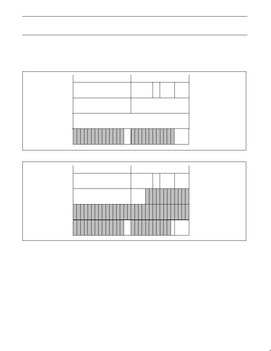
12.5.2.3
Block receive
The block receive format is shown below. The first quadlet contains the destination node ID and the rest of the packet header. The second and
third quadlets contain 16-bit sourceID and either the 48-bit destination offset (for requests) or the response code and reserved data (for
responses). The fourth quadlet contains the length of the data field and the extended transaction code (all zeros except for lock transactions).
The block data, if any, follows the extended code. The last quadlet contains packet reception status.
dataLength
extendedTcode
Block data
padding (if needed)
destinationID
tLabel
rt
tCode
priority
29 28 27 26 25 24 23 22 21 20 19 18 17 16 15 14 13 12 11 10 9 8 7 6 5 4 3 2 1 0
destinationOffsetHigh
destinationOffsetLow
sourceID
SV00262
spd
ackSent
31 30
Figure 19. Block Write or Lock Request Receive Format
Philips Semiconductors
Preliminary specification
PDI1394L21
1394 full duplex AV link layer controller
1999 Aug 06
22
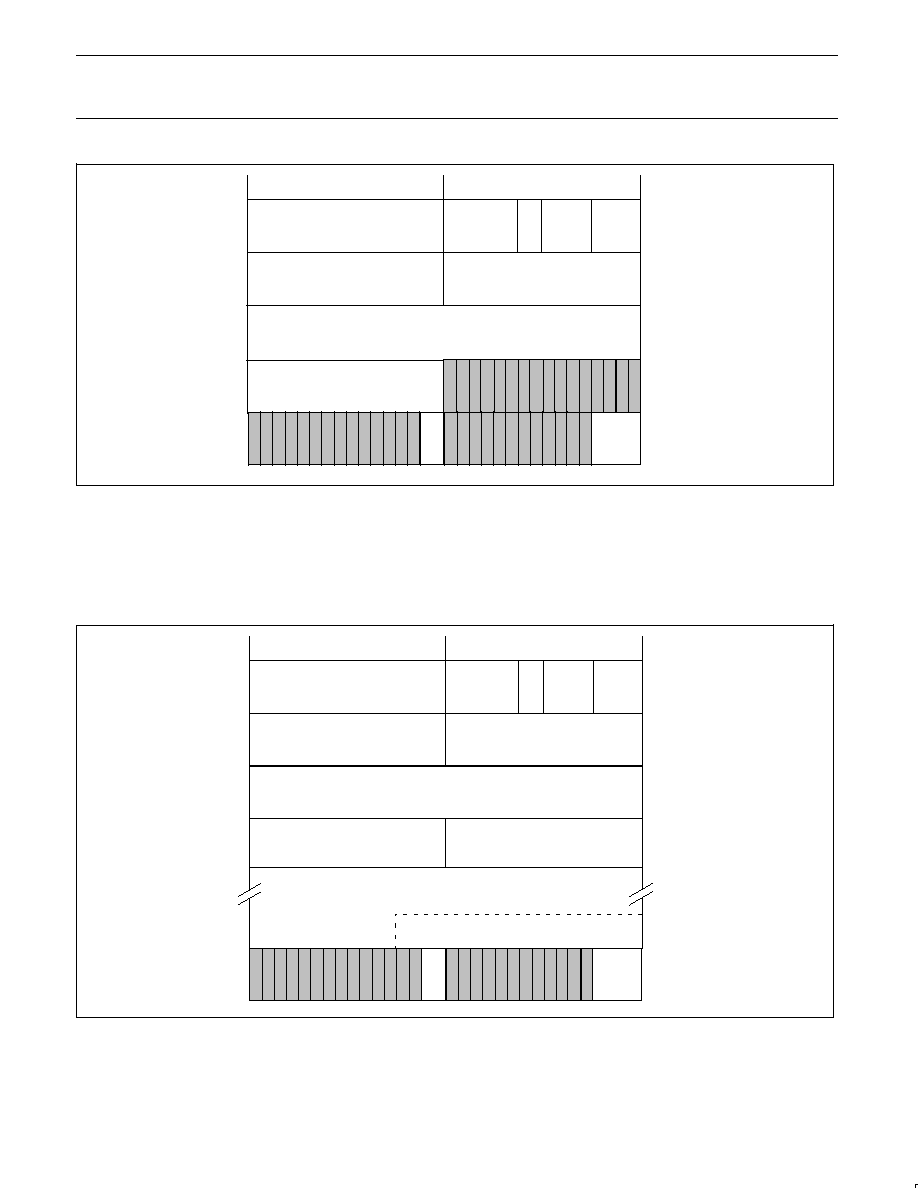
destinationID
tLabel
rt
tCode
priority
29 28 27 26 25 24 23 22 21 20 19 18 17 16 15 14 13 12 11 10 9 8 7 6 5 4 3 2 1 0
rCode
sourceID
dataLength
extendedTcode
Block data
padding (if needed)
SV00263
spd
ackSent
31 30
u
Figure 20. Block Read or Lock Response Receive Format
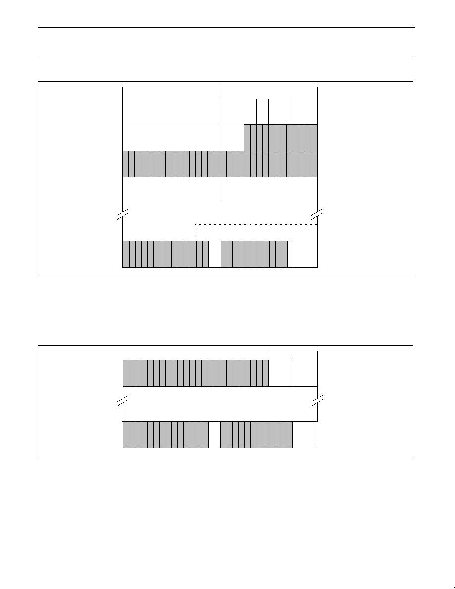
12.5.2.4
Self-ID and PHY packets receive
The self-ID and PHY packet receive formats are shown below. The first quadlet contains a synthesized packet header with a tCode of 0xE
(hex). For self-ID information, the remaining quadlets contain data that is received from the time a bus reset ends to the first subaction gap. This
is the concatenation of all the self-ID packets received. Note that the bit-inverted check quadlet is included in the Read Request FIFO and the
application must check it.
29 28 27 26 25 24 23 22 21 20 19 18 17 16 15 14 13 12 11 10 9 8 7 6 5 4 3 2 1 0
self ID packet data
1110
2
0000
2
SV00264
00
ackSent
3130
Figure 21. Self-ID Receive Format
The "ackSent" field will either be "ACK_DATA_ERROR" if a non-quadlet-aligned packet is received or there was a data overrun, or
"ACK_COMPLETE" if the entire string of self-ID packets was received.
Philips Semiconductors
Preliminary specification
PDI1394L21
1394 full duplex AV link layer controller
1999 Aug 06
23
29 28 27 26 25 24 23 22 21 20 19 18 17 16 15 14 13 12 11 10 9 8 7 6 5 4 3 2 1 0
PHY packet first quadlet
1110
2
0000
2
SV00265
31 30
Figure 22. PHY Packet Receive Format
For PHY packets, there is a single following quadlet which is the first quadlet of the PHY packet. The check quadlet has already been verified
and is not included.
12.5.2.5
Transaction data confirmation formats
After a packet from one of the queues has been transmitted, the asynchronous transmitter assembles a confirmation (see Figure 23) which is
used to confirm the result of the transmission to the higher layers. Separate confirmations are assembled for request and response
transmissions. Request confirmations are written into the receiver request queue and response confirmations are written into the receiver
response queue.
29 28 27 26 25 24 23 22 21 20 19 18 17 16 15 14 13 12 11 10 9 8 7 6 5 4 3 2 1 0
conf
destinationID
tLabel
3130
1000
2
00
2
SV00821
Figure 23. Request and response confirmation format
Table 7.
Confirmation codes
CODE
1
DESCRIPTION
0
Non-broadcast packet transmitted; addressed node returned no acknowledge (transaction complete).
1
Broadcast packet transmitted or non-broadcast packet transmitted; addressed node returned an acknowledge complete
(transaction complete).
2
Non-broadcast packet transmitted; addressed node returned an acknowledge pending.
4
Retry limit exceeded; destination node hasn't accepted the non-broadcast packet within the maximum number of retries
(transaction complete).
D
16
Acknowledge data error received (transaction complete).
E
16
Acknowledge type error received (transaction complete).
NOTE:
1. All other codes are reserved.
For every packet written in a transmitter queue by the CPU, there will be one confirmation written in the corresponding receiver queue by the AV
layer logic.
Philips Semiconductors
Preliminary specification
PDI1394L21
1394 full duplex AV link layer controller
1999 Aug 06
24
12.5.3
Interrupts
The PDI1394L21 provides a single interrupt line (HIF INT_N) for connection to a host controller. Status indications from four major areas of the
device are collected and ORed together to activate HIF INT_N. Status from four major areas of the device are collected in four status registers;
LNKPHYINTACK, ITXINTACK, IRXINTACK, and ASYINTACK. At this level, each individual status can be enabled to generate a chip-level
interrupt by activating HIF INT_N. To aid in determining the source of a chip-level interrupt, the major area of the device generating an interrupt
is indicated in the lower 4 bits of the GLOBCSR register. These bits are non-latching Read-Only status bits and do not need to be
acknowledged. To acknowledge and clear a standing interrupt, the bit in LNKPHYINTACK, ITXINTACK, IRXINTACK, or ASYINTACK causing
the interrupt status has to be written to a logic `1'; Note: Writing a value of `0' to the bit has no effect.
12.5.3.1
Determining and Clearing Interrupts
When responding to an interrupt event generated by the PDI1394L21, or operating in polled mode, the first register examined is the GLOBCSR
register. The least significant nibble contains interrupt status bits from general sections of the device; the link layer controller, the AV transmitter,
the AV receiver, and the asynchronous transceiver. The bits in GLOBCSR[3:0] are self clearing status bits. They represent the logical OR of all
the enabled interrupt status bits in their section of the AV Link Layer Controller.
Once an interrupt, or status is detected in GLOBCSR, the appropriate interrupt status register needs to be read, see the Interrupt Hierarchy
diagram for more detail. After all the interrupt indications are dealt with in the appropriate interrupt status register, the interrupt status indication
will automatically clear in the GLOBCSR.
All interrupt status bits in the various interrupt status registers are latching unless otherwise noted.
12.5.3.2
Interrupt Hierarchy
18 17 16 15 14 13 12 11 10 9 8 7 6 5 4 3 2 1 0
SV01076
7 6 5 4 3 2 1 0
3 2 1 0
ITXINTACK (0x02C)
IRXINTACK (0x04C)
ASYINTACK (0x0A0)
LNKPHYINTACK (0x008)
GLOBCSR (0x018)
HIF INT_N
PHYINT
CMDRST
F
AIRGAP
PHYRRX
ITBADFMT
PHYRST
A
TBADFMT
SNT_REJ
HDRERR
ARBGAP
CYST
AR
T
TCERR
CYTMOUT
CYDONE
CYPEND
CYLOST
CYSEC
INPERR
TRMSYT
TRMBP
DISCARD
ITXFULL
ITXEMPTY
DBCERR
SEQERR
IRXFULL
IRXEMPTY
CRCERR
CIPT
AGFL
T
RCVBP
FSYNC
SQOV
ASYTX/RX
ITXINT
IRXINT
LNKPHYINT
16 15 14 13 12 11 10 9 8 7 6 5 4 3 2 1 0
TIMEOUT
RCVDRSP
RRSPQFULL
RREQQFULL
RREQQQA
V
RRSPQRDERR
RREQQRDERR
RRSPQQA
V
SIDQA
V
RREQQLASTQ
TRSPQFULL
RRSPQLASTQ
TREQQWRERR
TRSPQWR
TRSPQWRERR
TREQQFULL
TREQQWR
6 5 4 3 2 1 0
RxDA
T
A
IR512LFT
8
IR256LFT
9
7
IT512LFT
IT256LFT
8
IR100LFT
10
IT100LFT
9
Figure 24. Interrupt Hierarchy

Philips Semiconductors
Preliminary specification
PDI1394L21
1394 full duplex AV link layer controller
1999 Aug 06
25
13.0
REGISTER MAP
Registers are 32 bits (quadlet) wide and all accesses are always done on a quadlet basis. This means that it is not possible to write just the
lower 8 bits, and leave the other bits unaffected (see Section 12.3.2 for more information). The values written to undefined fields/bits are ignored
and thus DON'T CARE.
A full bitmap of all registers is listed in Table 8. The meaning of shading and bit cell values is as follows:
A bit/field with no name written in it and dark shading is reserved and not used.
A bit/field with a name in it and light shading is a READ ONLY (status) bit/field.
A one bit value (0 or 1) written at the bottom of a writeable (control) bit is the default value after power-on-reset.
Table 8.
Full Bitmap of all Registers (consists of three tables shown on the following pages)

Philips Semiconductors
Preliminary specification
PDI1394L21
1394 full duplex AV link layer controller
1999 Aug 06
26
REGISTER
ADDRESS
IDREG
0x000
LNKCTL
0x004
LNKPHYINTE
0x00C
CYCTM
0x010
PHYACS
0x014
GLOBCSR
0x018
ITXPKCTL
0x020
ITXHQ1
0x024
<RESERVED>
0x01C
24
23
16
15
8
7
0
31
LNKPHYINTACK
0x008
ITXHQ2
0x028
ITXINTACK
0x02C
ITXINTE
0x030
EDISCARD
EITXFULL
EITXEMPTY
EDBCERR
EINPERR
ETRMBP
ETRMSYT
DISCARD
ITXFULL
ITXEMPTY
DBCERR
INPERR
TRMBP
TRMSYT
FMT
FDF
SYT
SPH
QPC
FN
DBS
EN_ITX
EN_FS
RST_ITX
PM
TRDEL
MAXBL
DIRA
V1
ASYTX/RX
ITXINT
IRXINT
LNKIPHYINT
EASYTX/RX
EITXINT
EIRXINT
ELNKPHYINT
RDPHY
WRPHY
PHYRGAD
PHYRGDATA
PHYRXAD
PHYRXDATA
CYCLE_SECONDS
CYCLE_NUMBER
CYCLE_OFFSET
ECMDRST
EF
AIRGAP
EHDRERR
ETCERR
EARBGAP
EPHYINT
ESNT_REJ
EITBADFMT
EA
TBADFMT
EPHYRRX
ECYTMOUT
EPHYRST
ECYPEND
ECYST
AR
T
ECYSEC
ECYLOST
CMDRST
F
AIRGAP
HDRERR
TCERR
ARBGAP
PHYINT
SNT_REJ
ITBADFMT
A
TBADFMT
PHYRRX
CYTMOUT
PHYRST
CYDONE
CYPEND
CYST
AR
T
CYSEC
CYLOST
IDV
ALID
RCVSELFI
D
ROOT
BUSYFLAG
CYTMREN
STRICTISOCH
CYMASTER
CYSOURCE
RST
Tx
RST
Rx
TxENABLE
RxENABLE
BSYCTRL
ATACK
NODE ID
BUS ID
0
0
0
0
0
0
0
0
0
0
0 0
0
0
0
0
0
0
0
0
0
0
0
0
0
0
0
0
0
0
0
0
0
0
0
1
0
0 0
0
0
0
0
0
0 0
0
0
0
0
0
0
0
0
0
0
0
0
0 0
0
0
0
0
0
0
0
0
0
0
0
0
0
0
0
0
0
0
0
0
0
0
0
0
0
1
0
0
0
0
0
0
0
0
0
0
0
0
0
0
0
0
0
0
0
0
0
0
0
0
0
0
0 0
0
0
0
0
0
0
0
0
0
0
0
0
0
0
0
0
0
0
0
0
0
0
0
0
0
0
0
0
0 0
0
0
0
0
0
0
0
0
0
0
0
0
0
0
0 0
0
0
0
0
0
0
0
0
0
0
0
0
0
0
0
0
1
1
0
1
VERSION CODE
SV00883
ENOUT
A
V
2
ENOUT
A
V
1
0
0
TXAP_CLK
0
0
SYT_DELA
Y
0
0
TxRDY
0
IT512LFT
0
IT256LFT
0
EIT256LFT
0
EIT512LFT
0
1
1
PART CODE
RxDA
T
A
0
ERxDA
T
A
0
ECYDONE
0
ENXTMSTP
0
IT100LFT
0
EIT100LFT
0
Philips Semiconductors
Preliminary specification
PDI1394L21
1394 full duplex AV link layer controller
1999 Aug 06
27
REGISTER
ADDRESS
ITXCTL
0x034
ITXMEM
0x038
IRXPKCTL
0x040
IRXHQ1
0x044
IRXHQ2
0x048
IRXINTACK
0x04C
IRXINTE
0x050
IRXCTL
0x054
IRXMEM
0x058
<RESERVED>
0x05C
<RESERVED>
0x07C
SV00884
IRXMAF
IRXM5A
V
IRXME
IRXMF
TAG
CHANNEL
ERR
SPD
0
0
0
0
0
0
0
0
ECIPT
AGFL
T
ERCVBP
ESQOV
ECRCERR
EIRXEMPTY
EFSYNC
ESEQERR
EIRXFULL
0
0
0
0
0
0
0
0
CIPT
AGFL
T
RCVBP
SQOV
CRCERR
IRXEMPTY
FSYNC
SEQERR
IRXFULL
0
0
0
0
0
0
0
0
E1
F1
FMT
SYT
FDF
SPH
QPC
FN
DBS
E0
F0
SID
24
23
16
15
8
7
0
31
EN_FS
RST_IRX
EN_IRX
SP
A
V
RMVUAP
BPAD
<RESERVED>
0x03C
.
.
.
ITXMAF
ITXM5A
V
ITXME
ITXMF
TAG
CHANNEL
SPD
0
0
0
0
0
0
0
0
0
0
0
0
0
1
0
0
0
0
1
RXAP_CLK
0
0
DIS_TSC
0
IR512LFT
0
IR256LFT
0
EIR256LFT
0
EIR512LFT
0
SNDIMM
0
ITM512LFT
ITM256LFT
IRM512LFT
IRM256LFT
ODD/EVEN
ODD/EVEN
ITM100LFT
IR100LFT
0
EIR100LFT
0
IRM100LFT

Philips Semiconductors
Preliminary specification
PDI1394L21
1394 full duplex AV link layer controller
1999 Aug 06
28
ETIMEOUT
ERCVDRSP
ERRSPQFULL
ERREQQFULL
ERREQQQA
V
ERRSPQRDERR
ERREQQRDERR
ERRSPQQA
V
ESIDQA
V
ERREQQLASTQ
ETRSPQFULL
ERRSPQLASTQ
ETREQQWRERR
ETRSPQWR
ETRSPQWRERR
ETREQQFULL
ETREQQWR
TIMEOUT
RCVDRSP
RRSPQFULL
RREQQFULL
RREQQQA
V
RRSPQRDERR
RREQQRDERR
RRSPQQA
V
SIDQA
V
RREQQLASTQ
TRSPQFULL
RRSPQLASTQ
TRSPQWR
TRSPQWRERR
TREQQFULL
TREQQWR
(WRITE ONLY)
LAST QUADLET OF PACKET FOR TRANSMITTER REQUEST QUEUE
(WRITE ONLY)
FIRST/MIDDLE QUADLET OF PACKET FOR TRANSMITTER REQUEST QUEUE
TRSPQF
TRSPQAF
RRSPQF
RREQQE
RREQQF
RREQQAF
RREQQ5A
V
RRSPQAF
RRSPQE
TRSPQ5A
V
RRSPQ5A
V
TREQQAF
TREQQ5A
V
TREQQF
TRSPQE
TREQQE
24
23
16
15
8
7
0
ARXALL
A
TXRST
ARXRST
MAXRC
TOS
TOF
31
SV00914
(WRITE ONLY)
LAST QUADLET OF PACKET FOR TRANSMITTER RESPONSE QUEUE
(WRITE ONLY)
FIRST/MIDDLE QUADLET OF PACKET FOR TRANSMITTER RESPONSE QUEUE
QUADLET OF PACKET FROM RECEIVER REQUEST QUEUE (TRANSFER REGISTER)
QUADLET OF PACKET FROM RECEIVER RESPONSE QUEUE (TRANSFER REGISTER)
TREQQWRERR
0
1
1
0
0
0
0
0
0
0
0
0
0
1
1
0
0 1
0
0
0
0
0
0
0
0
0
0
0
0
0
0
0
0 0
0
0
0
0
0
0
0
0
0
0
0
0
0
0
0
0 0
0
0
0
0
0
REGISTER
ADDRESS
ASYCTL
0x080
ASYMEM
0x084
TX_RQ_NEXT
0x088
TX_RQ_LAST
0x08C
TX_RP_NEXT
0x090
TX_RP_LAST
0x094
RREQ
0x098
RRSP
0x09C
ASYINTACK
0x0A0
ASYINTE
0x0A4
<RESERVED>
0x0A8
<RESERVED>
0x0F8
.
.
.
DIS_BCAST
0
TRSPQIDLE
TREQQIDLE
Philips Semiconductors
Preliminary specification
PDI1394L21
1394 full duplex AV link layer controller
1999 Aug 06
29
13.1
Link Control Registers
13.1.1
ID Register (IDREG) Base Address: 0x000
The ID register is automatically updated by the attached PHY with the proper Node ID after completion of the bus reset.
29 28 27 26 25 24 23 22 21 20 19 18 17 16 15 14 13 12 11 10 9 8 7 6 5 4 3 2 1 0
SV00915
NODE ID
BUS ID
VERSION CODE
3130
PART CODE
Reset Value 0xFFFF0101
Bit 31..22:
R/W
BUS ID: The 10-bit bus number that is used with the Node ID in the source address for outgoing packets and used to
accept or reject incoming packets. This field reverts to all `1's (0x3FF) upon bus reset.
Bit 21..16:
R/W
NODE ID: Used in conjunction with Bus ID in the source address for outgoing packets and used to accept or reject
incoming packets. This register auto-updates with the node ID assigned after the 1394 bus Tree-ID sequence.
Bit 15..8:
R
PART CODE: "01" designates PDI1394L21.
Bit 7..0:
R
VERSION CODE: "02" shows this is revision level 2 of this part.
13.1.2
General Link Control (LNKCTL) Base Address: 0x004
The General Link control register is used to program the Link Layer isochronous transceiver, as well as the overall link transceiver. It also
provides general link status.
29 28 27 26 25 24 23 22 21 20 19 18 17 16 15 14 13 12 11 10 9 8 7
6
5 4 3
2 1
0
SV00892
IDV
ALID
RCVSELFID
ROOT
BUSYFLAG
CYTMREN
STRICTISOCH
CYMASTER
CYSOURCE
RST
Tx
RST
Rx
TxENABLE
RxENABLE
BSYCTRL
ATACK
31 30
TxRDY
RPL
DA
T
AINV
L
TLEND
Reset Value 0x46000002
Bit 31:
R/W
IDValid (IDVALID): When equal to one, the PDI1394L21 accepts the packets addressed to this node. This bit is
automatically set after selfID complete and node ID is updated.
Bit 30:
R/W
Receive Self ID (RCVSELFID): When asserted, the self-identification packets, generated by each PHY device on the
bus, during bus initialization are received and placed into the asynchronous request queue as a single packet. Bit 30
also enables the reception of PHY configuration packets in the asynchronous request queue.
Bit 29..27:
R/W
Busy Control (BSYCTRL): These bits control what busy status the chip returns to incoming packets. The field is
defined below:
000 = use protocol requested by received packet (either dual phase or single phase)
001 = send busy A when it is necessary to send a busy acknowledge (testing/diagnostics)
010 = send a busy B when it is necessary to send a busy acknowledge (testing/diagnostics)
011 = use single phase retry protocol
100 = use protocol requested in packet, always send a busy ack (for all packets)
101 = busy A all incoming packets
110 = busy B all incoming packets are `1'
111 = use single phase retry protocol, always send a busy ack
Bit 26:
R/W
Transmitter Enable (TxENABLE): When this bit is set, the link layer transmitter will arbitrate and send packets.
Bit 25:
R/W
Receiver Enable (RxENABLE): When this bit is set, the link layer receiver will receive and respond to bus packets.
Bit 21:
R/W
Reset Transmitter (RSTTx): When set to one, this synchronously resets the transmitter within the link layer.
Bit 20:
R/W
Reset Receiver (RSTRx): When set to one, this synchronously resets the receiver within the link layer.
Bit 12:
R/W
Strict Isochronous (STRICTISOCH): Used to accept or reject isochronous packets sent outside of specified
isochronous cycles (between a Cycle Start and subaction gap). A `1' rejects packets sent outside the specified
cycles, a "0" accepts isochronous packets sent outside the specified cycle.
Bit 11:
R/W
Cycle Master (CYMASTER): When asserted and the PDI1394L21 is attached to the root PHY (ROOT bit = 1), and
the cycle_count field of the cycle timer register increments, the transmitter sends a cycle-start packet. Cycle Master
function will be disabled if a cycle timeout is detected (CYTMOUT bit 5 in LNKPHYINTACK). To restart the Cycle
Master function in such a case, first reset CYMASTER, then set it again.

Philips Semiconductors
Preliminary specification
PDI1394L21
1394 full duplex AV link layer controller
1999 Aug 06
30
Bit 10:
R/W
Cycle Source (CYSOURCE): When asserted, the cycle_count field increments and the cycle_offset field resets for
each positive transition of CYCLEIN. When deasserted, the cycle count field increments when the cycle_offset field
rolls over.
Bit 9:
R/W
Cycle Timer Enable (CYTIMREN): When asserted, the cycle offset field increments.
Bit 6:
R
Transmitter Ready (TxRDY): The transmitter is idle and ready.
Bit 5:
R
Root (ROOT): Indicates this device is the root on the bus. This automatically updates after the self_ID phase.
Bit 4:
R
Busy Flag (BUSYFLAG): The type of busy acknowledge which will be sent next time an acknowledge is required.
0 = Busy A, 1 = Busy B (only meaningful during a dual-phase busy/retry operation).
Bit 3..0:
R
AT acknowledge received (ATACK): The last acknowledge received by the transmitter in response to a packet sent
from the transmit-FIFO interface while the ATF is selected (diagnostic purposes).
13.1.3
Link /Phy Interrupt Acknowledge (LNKPHYINTACK) Base Address: 0x008
The Link/Phy Interrupt Acknowledge register indicates various status and error conditions in the Link and Phy which can be programmed to
generate an interrupt. The interrupt enable register (LNKPHYINTE) is a mirror of this register. Acknowledgment of an interrupt is accomplished
by writing a `1' to a bit in this register that is set. This action reset the bit indication to a `0'. Writing a `1' to a bit that is already "0" will have no
effect on the register.
29 28 27 26 25 24 23 22 21 20 19 18 17 16 15 14 13 12 11 10 9 8 7 6 5 4 3 2 1 0
SV00893
CMDRST
F
AIRGAP
HDRERR
TCERR
ARBGAP
PHYINT
SNT_REJ
ITBADFMT
A
TBADFMT
PHYRRX
CYTMOUT
PHYRST
CYDONE
CYPEND
CYST
AR
T
CYSEC
CYLOST
31 30
RxDA
T
A
Reset Value 0x00000000
Bit 18:
R/W
Command Reset Received (CMDRST): A write request to RESET-START has been received.
Bit 17:
R/W
Fair Gap (FAIRGAP): The serial bus has been idle for a fair-gap time (called subaction gap in the IEEE 1394
specification).
Bit 16:
R/W
Arbitration Reset Gap (ARBGAP): The serial bus has been idle for an arbitration reset gap.
Bit 15:
R/W
Phy Chip Int (PHYINT): The Phy chip has signaled an interrupt through the Phy interface. This bit becomes active for
any of the following reasons (1) PHY has detected a loop on the bus, (2) cable power has fallen below the minimum
voltage, (3) the PHY arbitration state machine has timed-out usually indicative of a bus loop, (4) a bus cable has
been disconnected. Typically, recognition and notification of any of the above events by the PHY requires between
166 and 500 microseconds; therefore, this bit is not instantaneously set.
Bit 14:
R/W
Phy Register Information Received (PHYRRX): A register has been transferred by the Physical Layer device into the
Link.
Bit 13:
R/W
Phy Reset Started (PHYRST): A Phy-layer reconfiguration has started. This interrupt clears the ID valid bit. (Called
Bus Reset in the IEEE 1394 specification).
Bit 11:
R/W
Receiver has data (RxDATA): The receiver has confirmed data to the receiver response/request FIFO.
Bit 10:
R/W
Isochronous Transmitter is Stuck (ITBADFMT): The transmitter has detected invalid data at the transmit-FIFO
interface when the ITF is selected.
Bit 9:
R/W
Asynchronous Transmitter is Stuck (ATBADFMT): The transmitter expected start of new async packet in queue, but
found other data (out of sync with user). Reset to clear.
Bit 8:
R/W
Busy Acknowledge Sent by Receiver (SNT_REJ): The receiver was forced to send a busy acknowledge to a packet
addressed to this node because the receiver response/request FIFO overflowed.
Bit 7:
R/W
Header Error (HDRERR): The receiver detected a header CRC error on an incoming packet that may have been
addressed to this node.
Bit 6:
R/W
Transaction Code Error (TCERR): The transmitter detected an invalid transaction code in the data at the transmit
FIFO interface.
Bit 5:
R/W
Cycle Timed Out (CYTMOUT): ISOCH cycle lasted more than 125
µ
s from Cycle-Start to Fair Gap: Disables cycle
master function
Bit 4:
R/W
Cycle Second incremented (CYSEC): The cycle second field in the cycle-timer register incremented. This occurs
approximately every second when the cycle timer is enabled.
Bit 3:
R/W
Cycle Started (CYSTART): The transmitter has sent or the receiver has received a cycle start packet.
Bit 2:
R/W
Cycle Done (CYDONE): A fair gap has been detected on the bus after the transmission or reception of a cycle start
packet. This indicates that the isochronous cycle is over; Note: Writing a value of `0' to the bit has no effect.
Bit 1:
R/W
Cycle Pending (CYPEND): Cycle pending is asserted when cycle timer offset is set to zero (rolled over or reset) and
stays asserted until the isochronous cycle has ended.
Bit 0:
R/W
Cycle Lost (CYLOST): The cycle timer has rolled over twice without the reception of a cycle start packet. This only
occurs when cycle master is not asserted.

Philips Semiconductors
Preliminary specification
PDI1394L21
1394 full duplex AV link layer controller
1999 Aug 06
31
13.1.4
Link / Phy Interrupt Enable (LNKPHYINTE) Base Address: 0x00C
This register is a mirror of the Link/Phy Interrupt Acknowledge (LNKPHYINTACK) register. Enabling an interrupt is accomplished by writing a `1'
to the bit corresponding to the interrupt desired.
This register enables the interrupts described in the Link /Phy Interrupt Acknowledge register (LNKPHYINTACK) description. A one in any of the
bits enables that function to create an interrupt. A zero disables the interrupt, however the status is readable in the Link /Phy Interrupt
Acknowledge register.
29 28 27 26 25 24 23 22 21 20 19 18 17 16 15 14 13 12 11 10 9 8
7 6
5 4 3
2 1
0
ECMDRST
EF
AIRGAP
EHDRERR
ETCERR
EARBGAP
EPHYINT
ESNT_REJ
EITBADFMT
EA
TBADFMT
EPHYRRX
ECYTMOUT
EPHYRST
ECYDONE
ECYPEND
ECYST
AR
T
ECYSEC
ECYLOST
SV00894
31 30
ETIMER
EAUTH DN
Reset Value 0x00000000
Bits 18..0 are interrupt enable bits for the Link/Phy Interrupt Acknowledge (LNKPHYINTACK).
13.1.5
Cycle Timer Register (CYCTM) Base Address: 0x010
Cycle Timer Register operation is controlled by the Cycle Timer Enable (CYTMREN) bit in the Link Control Register (LNKCTL, 0x004).
29 28 27 26 25 24 23 22 21 20 19 18 17 16 15 14 13 12 11 10 9 8 7 6 5 4 3 2 1 0
CYCLE_SECONDS
CYCLE_NUMBER
CYCLE_OFFSET
SV00276
3130
Reset Value 0x00000000
Bit 31..25:
R/W
Seconds count: 1-Hz cycle timer counter.
Bit 24..12:
R/W
Cycle Number: 8kHz cycle timer counter.
Bit 11..0:
R/W
Cycle Offset: 24.576MHz cycle timer counter.
13.1.6
Phy Register Access (PHYACS) Base Address: 0x014
This register provides access to the internal registers on the Phy. There are special considerations when reading or writing to this register. When
reading a PHY register, the address of the register is written to the PHYRGAD field with the RDPHY bit set. The PHY data will be valid when the
PHYRRX bit (LNKPHYINTACK register bit 14) is set. Once this happens the register data is available in the PHYRXDATA, the address of the
register just read is also available in the PHYRXAD fields. When writing a Phy register, the address of the register to be written is set in the
PHYRGAD field and the data to be written to the register is set in PHYRGDATA, along with the WRPHY bit being set. Once the write is
complete, the WRPHY bit will be cleared. Do not write a new Read/Write command until the previous one has been completed. After the Self-ID
phase, PHY register 0 will be read automatically.
29 28 27 26 25 24 23 22 21 20 19 18 17 16 15 14 13 12 11 10 9 8 7 6 5 4 3 2 1 0
RDPHY
WRPHY
SV00277
PHYRGAD
PHYRGDATA
PHYRXAD
PHYRXDATA
31 30
Reset Value 0x00000000
Bit 31:
R/W
Read Phy Chip Register (RDPHY): When asserted, the PDI1394L21 sends a read register request with address
equal to Phy Rg Ad to the Phy interface. This bit is cleared when the request is sent.
Bit 30:
R/W
Write Phy Chip Register (WRPHY): When asserted, the PDI1394L21 sends a write register request with address
equal to Phy Rg Ad to the Phy interface. This bit is cleared when the request is sent.
Bit 27..24:
R/W
Phy Chip Register Address (PHYRGAD): This is the address of the Phy-chip register that is to be accessed.
Bit 23..16:
R/W
Phy Chip Register Data (PHYRGDATA): This is the data to be written to the Phy-chip register indicated in Phy Rg Ad.
Bit 11..8:
R
Phy Chip Register Received Address (PHYRXAD): Address of register from which Phy Rx Data came.
Bit 7..0:
R
Phy Chip Register Received Data (PHYRXDATA): Data from register addressed by Phy Rx Ad.
Philips Semiconductors
Preliminary specification
PDI1394L21
1394 full duplex AV link layer controller
1999 Aug 06
32
13.1.7
Global Interrupt Status and TX Control (GLOBCSR) Base Address: 0x018
This register is the top level interrupt status register. If the external interrupt line is set, this register will indicate which major portion of the AV
Link generated the interrupt. There is no interrupt acknowledge required at this level. These bits auto clear when the interrupts in the
appropriate section of the device are cleared or disabled. Control of the AV transceiver is also provided by this register.
Bits 0 to 3 are used to identify which internal modules are currently generating an interrupt. After identifying the module, the appropriate register
in that module must be read to determine the exact cause of the interrupt.
NOTES
1. There can be more than one interrupt source active at the same time.
2. The HIF INT_N signal (pin 28) remains active as long as there is at least one more enabled active interrupt status bit.
29 28 27 26 25 24 23 22 21 20 19 18 17 16 15 14 13 12 11 10
9
8
7
6
5
4
3
2
1
0
ASYTX/RX
ITXINT
IRXINT
LNKPHYINT
31 30
EASYTX/RX
EITXINT
EIRXINT
ELNKPHYINT
DIRA
V1
ENOUT
A
V
2
ENOUT
A
V
1
SV00857
Reset Value 0x00010000
Bit 18:
R/W
Enable output AVPORT2: A `1' enables AVPORT2 as an output. A `0' sets the 3-State condition on the port. In
3-State condition the port may be used as an input or unused output according to the state of DIRAV1 (bit 16).
Bit 17:
R/W
Enable output AVPORT1: A `1' enables AVPORT1 as an output. A `0' sets the 3-State condition on the port. In
3-State condition the port may be used as an input or unused output according to the state of DIRAV1 (bit 16).
Bit 16:
R/W
Direction of AVPORT1 (DIRAV1): A `1' enables AVPORT1 as a transmitter, thus AVPORT1 pins are inputs. A `0'
configures AVPORT1 as a receiver, AVPORT1 pins are outputs in this configuration. The configuration of AVPORT2
pins is opposite of AVPORT1 pins. When AVPORT1 is set to transmit, AVPORT2 receives and vice versa.
Bit 11:
R/W
Enables generation of external interrupt by asynchronous transmitter and receiver module (ASYTX/RX, bit 3) when
set (1). Disables such interrupts when clear (0) (regardless of ASYINTE contents).
Bit 10:
R/W
Enables generation of external interrupt by the isochronous transmitter module (ITXINT, bit 2) when set (1).
Disables such interrupts when clear (0) (regardless of ITXINTE contents).
Bit 9:
R/W
Enables generation of external interrupt by the isochronous receiver module (IRXINT, bit 1) when set (1).
Disables such interrupts when clear (0) (regardless of IRXINTE contents).
Bit 8:
R/W
Enables generation of external interrupt by general link/phy module (LKPHYINT, bit 0) when set (1). Disables such
interrupts when clear (0) (regardless of LNKPHYINTE contents).
Bit 3:
R
Asynchronous Transmitter/Receiver Interrupt (ASYITX/RX): Interrupt source is in the Asynchronous Transmitter/
Receiver Interrupt Acknowledge/Source register.
Bit 2:
R
AV Transmitter Interrupt (ITXINT): Interrupt source is in the AV Transmitter Interrupt Acknowledge/Source register.
Bit 1:
R
AV Receiver Interrupt (IRXINT): Interrupt source is in the AV Receiver Interrupt Acknowledge/Source register.
Bit 0:
R
Link-Phy Interrupt (LNKPHYINT): Interrupt source is in the Link Phy Interrupt Acknowledge register.
Philips Semiconductors
Preliminary specification
PDI1394L21
1394 full duplex AV link layer controller
1999 Aug 06
33
13.2
AV (Isochronous) Transmitter and Receiver Registers
13.2.1
Isochronous
Transmit Packing Control and Status (ITXPKCTL) Base Address: 0x020
This register allows the user to set up the appropriate AV packets from data entered into the AV interface. The packing and control parameters
(TRDEL, MAXBL, DBS, FN, QPC, and SPH) should never be changed while the transmitter is operating. The only exception to this is the
MAXBL parameter when in MPEG-2 packing mode.
NOTE: When reset of isochronous transmitter is necessary, first disable the transmitter (place bit 4, EN_ITX, LOW), wait for FIFO to empty, then
reset the transmitter (place RST_ITX, bit 0, HIGH). This procedure will ensure that data in the FIFO is transmitted before reset.
29 28 27 26 25 24 23 22 21 20 19 18 17 16 15 14 13 12 11 10 9 8 7 6 5 4 3 2 1 0
EN_ITX
EN_FS
RST_ITX
SV00886
PM
TRDEL
MAXBL
31 30
TXAP_CLK
SYT_DELA
Y
ENXTMSTP
mLAN
Reset Value 0x00000001
Bit 29..28:
R/W
TXAP_CLK: Application Clock, default mode, `00' the AVxCLK pin is an input. This pin can become an application
clock for the isochronous Transmitter (and output) by programming it to `01', `10', or `11'.
The programming values are:
00
Input
01
24.576MHz
10
12.288MHz
11
6.144MHz
Note that when enabled as `01', `10', or `11', the AV port that is configured as transmitter and enabled will output this
clock signal on its AVxCLK pin.
Bit 27..16:
R/W
TRDEL: Transport delay. Value added to cycle timer to produce time stamps. Lower 4 bits add to upper 4 bits of
cycle_offset, (Cycle Timer Register, CYCTM). Remainder adds to cycle_count field.
Bit 15..8:
R/W
MAXBL: The (maximum) number of data blocks to be put in a payload.
Bit 7:
R/W
ENXTMSTP: Enable External time stamp control. Allows an external time stamp (generated by the application) to be
inserted in place of the link-generated time stamp. Defaults to link generated time stamp. The application must
present the first byte of a quadlet-wide time stamp accompanied by the AVSYNC pulse (and AVVALID) to the
AVPORT. The external time stamp quadlet is inputted first, followed by the application data packet. The transmitted
packet size is now one quadlet larger than the original isochronous data packet--Set up the isochronous
transmitter accordingly with SPH = 1. CAUTION: Unless valid IEC 61883 time stamp format (based on the link cycle
timer) is used, the receiving node link chip must be equipped with a time stamp check disabling function similar to
the DIS_TSC bit (register 0X040, Bit 7). Please see section 13.2.8 for details.
Bit 6..5:
R/W
SYT_DELAY: Programmable delay of AV1FSYNC and AV2FSYNC. Each cycle is 1 bus cycle, 125
m
s.
Reset value is "00", a 3 cycle delay.
01 = 2 cycles
00 = 3 cycles
10 = 4 cycles
11 = Reserved
Bit 4:
R/W
EN_ITX: Enable receipt of new application packets and generation of isochronous bus packets in every cycle. This
bit also enables the Link Layer to arbitrate for the transmitter in each subsequent bus cycle. When this bit is disabled
(0), the current packet will be transmitted and then the transmitter will shut down.
Bit 3..2:
R/W
PM: packing mode:
00 = variable sized bus packets, most generic mode.
01 = fixed size bus packets.
10 = MPEG2 packing mode.
11 = No data, just CIP headers are transmitted.
Bit 1:
R/W
EN_FS:enable generation/insertion of SYT stamps (Time Stamps) in CIP header.
Bit 0:
R/W
Reset Isochronous Transmitter (RST_ITX): causes transmitter to be reset when `1'. In order for synchronous reset of
ITX to work properly, an AVxCLK (from either the internal or external source) must be present and ensure that the
reset bit is kept (programmed) HIGH for at least the duration of one AVxCLK period. Failure to do so may cause
the application interface of this module to be improperly reset (or not reset at all). When reset is enabled, all bytes
will be flushed from the FIFO and transmission will cease immediately.

Philips Semiconductors
Preliminary specification
PDI1394L21
1394 full duplex AV link layer controller
1999 Aug 06
34
13.2.2
Common Isochronous Transmit Packet Header Quadlet 1 (ITXHQ1) Base Address: 0x024
The AV Transmit Packing Control register holds the specification for the packing scheme used on the AV data stream. This information is
included in Common Isochronous Packet (CIP) header quadlet 1.
29 28 27 26 25 24 23 22 21 20 19 18 17 16 15 14 13 12 11 10 9 8 7 6 5 4 3 2 1 0
SPH
QPC
FN
DBS
SV01747
31 30
Reset Value 0x00000000
Bit 16..23:
R/W
DBS: Size of the data blocks from which AV payload is constructed. The value 0 represents a length of 256 quadlets.
Bit 14..15:
R/W
FN: (Fraction Number) The encoding for the number of data blocks into which each source packet shall be divided
(00 = 1, 01 = 2, 10 = 4, 11 = 8).
Bit 11..13:
R/W
QPC: Number of dummy quadlets to append to each source packet before it is divided into data blocks of the
specified size. The value QPC must be less than DBS and less than 2
FN
.
Bit 10:
R/W
SPH: Indicates that a 25-bit CYCTM based time stamp has to be inserted before each application packet.
13.2.3
Common Isochronous Transmit Packet Header Quadlet 2 (ITXHQ2) Base Address: 0x028
The contents of this register are copied to the second quadlet of the CIP header and transmitted with each isochronous packet.
29 28 27 26 25 24 23 22 21 20 19 18 17 16 15 14 13 12 11 10 9 8 7 6 5 4 3 2 1 0
FMT
FDF
SV00281
31 30
SYT
Reset Value 0x00000000
Bit 29..24:
R/W
FMT: Value to be inserted in the FMT field in the AV header.
Bit 23..0:
R/W
FDF/SYT: Value to be inserted in the FDF field. When the EN_FS bit in the Transmit Control and Status Register
(ITXPKCTL) is set (=1), the lower 16 bits of this register are replaced by an SYT stamp if a rising edge on
AVFSYNCIN has been detected or all `1's if no such edge was detected since the previous packet. The upper 8 bits
of the register are sent as they appear in the FDF register. When the EN_FS bit in the Transmit Control and Status
Register is unset (=0), the full 24 bits can be set to any application specified value.

Philips Semiconductors
Preliminary specification
PDI1394L21
1394 full duplex AV link layer controller
1999 Aug 06
35
13.2.4
Isochronous Transmitter Interrupt Acknowledge (ITXINTACK) Base Address: 0x02C
The AV Transmitter Interrupt Control and Status register is the interrupt register for the AV transmitter.
Bits 2, 3, and 4 "auto repair" themselves, i.e. AVLINK will detect the situation and attempt to recover on its own. The host controller still needs to
clear these interrupts to be alerted the next time.
29 28 27 26 25 24 23 22 21 20 19 18 17 16 15 14 13 12 11 10 9 8 7 6 5 4 3 2 1 0
DISCARD
ITXFULL
ITXEMPTY
DBCERR
INPERR
TRMBP
TRMSYT
SV00882
31 30
IT512LFT
IT256LFT
IT100LFT
Reset Value 0x00000000
Bits 9 .. 0 are interrupt acknowledge bits; and are defined as:
Bit 9:
R/W
IT100LFT: Interrupt when transmitter queue reaches 100 quadlets from full. (924 of 1024 quadlets in queue)
Bit 8:
R/W
IT256LFT: Interrupt when transmitter queue reaches 256 quadlets from full. (768 of 1024 quadlets in queue)
Bit 7:
R/W
IT512LFT: Interrupt when transmitter queue reaches 50% of full. (512 of 1024 quadlets in queue)
Bit 6:
R/W
TRMSYT: Interrupt on transmission of a SYT in CIP header quadlet 2
Bit 5:
R/W
TRMBP: Interrupt on payload transmission/discard complete.
Bit 4:
R/W
DBCERR: Acknowledge interrupt on Data Block Count (DBC) synchronization loss.
Bit 3:
R/W
INPERR: Acknowledge interrupt on input error (input data discarded).
Bit 2:
R/W
DISCARD: Interrupt on lost cycle (payload discarded).
Bit 1:
R/W
ITXFULL: Interrupt on isochronous memory bank full. This is a fatal error, the recommended action is to reset and
re-initialize the transmitter.
Bit 0:
R/W
ITXEMPTY: Interrupt on isochronous memory bank empty.
Other bits will always read `0'.
13.2.5
Isochronous Transmitter Interrupt Enable (ITXINTE) Base Address: 0x030
These are the enabled bits for the AV Transmitter Control.
29 28 27 26 25 24 23 22 21 20 19 18 17 16 15 14 13 12 11 10 9
8
7
6
5 4
3
2 1
0
EDISCARD
EITXFULL
EITXEMPTY
EDBCERR
EINPERR
ETRMBP
ETRMSYT
31 30
SV00891
EIT512LFT
EIT256LFT
EIT100LFT
Reset Value 0x00000000
Bits 9..0 are interrupt enable bits for the Isochronous Transmitter Interrupt Acknowledge register (ITXINTACK).

Philips Semiconductors
Preliminary specification
PDI1394L21
1394 full duplex AV link layer controller
1999 Aug 06
36
13.2.6
Isochronous Transmitter Control Register (ITXCTL) Base Address: 0x34
29 28 27 26 25 24 23 22 21 20 19 18 17 16 15 14 13 12 11 10 9 8 7 6 5 4 3 2 1 0
SV01016
TAG
CHANNEL
SPD
31 30
ODD/EVEN
EMI_PE
CPHR_EN
SY
EMI
Reset Value 0x00000000
Bit 15..14:
R/W
Tag: Tag code to insert in isochronous bus packet header. Should be `01' for IEC 61883 International Standard data.
Bit 13..8:
R/W
Channel: Isochronous channel number.
Bit 5..4:
R/W
Speed: Cable transmission speed (S100, S200, S400).
00 = 100Mbs
01 = 200Mbs
10 = 400Mbs
11 = reserved
Bit 3..0
R
Sync: Code to insert in SY field of isochronous bus packet header. Bit 1 is odd/even bit used for encryption key
(0 = even, 1 = odd). Bit value determined by state of transmit port AVxENKEY pin. Some data encryption schemes
require that an ODD/EVEN bit accompany each application packet sent for the purpose of changing "keys" after
short intervals of time (makes breaking an encryption code more difficult). The PDI1394L21 uses the sync field
ODD/EVEN bit for this purpose. Data is inputted to the transmitting AV port accompanied by the state of the
ODD/EVEN bit presented to the AVx ENKEY pin. The pin state at the rising edge of the AVCLK as the first byte of
the packet determines the ODD/EVEN "key" state for that packet. The ODD/EVEN key state may change as often as
required, provided that 2 key changes do not appear in the transmit FIFO simultaneously. If this rule is observed, the
proper "key" state will accompany the packet on to the 1394 bus and through the receiving node's receive FIFO. As
the packet is being outputted at the receive node's PDI1394L21, the accompanying ODD/EVEN key state will be
output. The key state remains for all bytes of the packet. Typical change rates for the ODD/EVEN key are between
1 change per second and a change every 30 seconds.
13.2.7
Isochronous Transmitter Memory Status (ITXMEM) Base Address: 0x038
The AV Transmitter Memory Status register reports on the condition of the internal memory buffer used to store incoming AV data streams
before transmission over the 1394 bus.
29 28 27 26 25 24 23 22 21 20 19 18 17 16 15 14 13 12 11 10 9 8 7 6 5 4 3 2 1 0
ITXMAF
ITXM5A
V
ITXME
ITXMF
SV00916
3130
ITM512LFT
ITM256LFT
ITM100LFT
Reset Value 0x00000003
Bit 6:
R
ITM100LFT: Memory has 100 quadlets of space remaining before becoming full.
Bit 5:
R
ITM256LFT: Memory has 256 quadlets of space remaining before becoming full.
Bit 4:
R
IITM512LFT: Memory is
1
/
2
full.
Bit 3:
R
ITXMF: memory is completely full, no storage available.
Bit 2:
R
ITXMAF: almost full, exactly one quadlet of storage available.
Bit 1:
R
ITXM5AV: at least 5 more quadlets of storage available.
Bit 0:
R
ITXME: memory bank is empty (zero quadlets stored).
Philips Semiconductors
Preliminary specification
PDI1394L21
1394 full duplex AV link layer controller
1999 Aug 06
37
13.2.8
Isochronous Receiver Unpacking Control (IRXPKCTL) Base Address: 0x040
NOTE: When receiver reset is required, first disable receiver (EN_IRX = 0), then wait until Rx FIFO is emptied, then perform the reset. This will
allow previously received packets to go to the application instead of being lost.
29 28 27 26 25 24 23 22 21 20 19 18 17 16 15 14 13 12 11 10 9 8 7 6 5 4 3 2 1 0
EN_FS
RST_IRX
EN_IRX
SP
A
V
RMVUAP
SV00887
BPAD
31 30
RXAP_CLK
DIS_TSC
SNDIMM
Reset Value 0x00000041
AV Receiver Control Bits.
Bit 29..28:
R/W
RXAP_CLK: Receiver Application Clock, default mode, `00' the AVxCLK pin is an input. This pin can become an
application clock and output for the isochronous Receiver by programming it to `01', `10', or `11'.
The programming values are:
00
Input
01
24.576MHz
10
12.288MHz
11
6.144MHz
Note that when enabled as `01', `10', or `11', the AV port that is configured as receiver and enabled will output this
clock signal on its AVxCLK pin.
Bit 8:
R/W
SNDIMM: Send immediately; when set to "1", this bit will allow a received isochronous packet containing a CRC
error to be output immediately (without regard to the time stamp value). This bit defaults to "0". In default (reset)
mode, the packet will be output with respect to the time stamp value, even if there is a CRC error.
CAUTION: If there is an error in the time stamp, the packet may be held far into the future. This will affect
subsequently received packets.
Bit 7:
R/W
DIS_TSC: Disable Time Stamp Checking. Defaults to "0", time stamp checking is enabled. When time stamp
checking is disabled, the time stamp accompanying a packet is output before the packet to the application for use
by the application. This adds an extra quadlet of data to the received data stream; the application must be capable
of handling this extra 4 bytes. Note: The term "Time Stamp" used here refers only to source packet header (full
quadlet) time stamps; it does not mean SYT field hardware synchronization stamps. Also see ENXTMSTP bit in
register X020 for transmit node application time stamp formatting and inputting.
Bit 6:
R/W
RMVUAP: Remove unreliable packets from memory, do not attempt delivery
Bit 5:
R
SPAV: Source packet available for delivery in buffer memory.
Bit 4:
R/W
EN_IRX: Enable receiver operation. Value is only checked whenever a new bus packet arrives, so enable/disable
while running is `graceful', meaning any transfers in process will be completed before this bit is asserted.
Bit 2..3:
R/W
BPAD: Value indicating the amount of byte padding to be removed from the last data quadlet of each source packet,
from 0 to 3 bytes. This is in addition to quadlet padding as defined in IEC 61883 International Standard.
Bit 1:
R/W
EN_FS: Enable processing of SYT stamps.
Bit 0:
R/W
RST_IRX: causes the receiver to be reset when `1'. In order for synchronous reset of IRX to work properly, the
application must supply an AVCLK and ensure that the reset bit is kept (programmed) HIGH for at least the duration
of one AVCLK period. Failure to do so may cause the application interface of this module to be improperly reset (or
not reset at all).

Philips Semiconductors
Preliminary specification
PDI1394L21
1394 full duplex AV link layer controller
1999 Aug 06
38
13.2.9
Common Isochronous Receiver Packet Header Quadlet 1 (IRXHQ1) Base Address: 0x044
This quadlet represents the last received header value when AV receiver is operating.
29 28 27 26 25 24 23 22 21 20 19 18 17 16 15 14 13 12 11 10 9 8 7 6 5 4 3 2 1 0
SPH
QPC
FN
DBS
SV00286
E0
F0
31 30
SID
Reset Value 0x00000000
Bit 31..30:
R
E0: End of Header, F0: Format: Always set to 00 for first AV header quadlet
Bit 29..24
R
SID: Source ID, contains the node address of the sender of the isochronous data.
Bit 23.16:
R
DBS: Size of the data blocks from which AV payload is constructed. The value 0 represents a length of 256 quadlets.
Bit 15..14:
R
FN (Fraction Number): The encoding for the number of data blocks into which each source packet has been divided
(00 = 1, 01 = 2, 10 = 4, 11 = 8) by the transmitter of the packet.
Bit 13..11:
R
QPC: Number of dummy quadlets appended to each source packet before it was divided into data blocks of the
specified size.
Bit 10:
R
SPH: Indicates that a CYCTM based time stamp is inserted before each application packet (25 bits specified in the
IEC 61883 International Standard).
13.2.10
Common Isochronous Receiver Packet Header Quadlet 2 (IRXHQ2) Base Address: 0x048
E1
F1
29 28 27 26 25 24 23 22 21 20 19 18 17 16 15 14 13 12 11 10 9 8 7 6 5 4 3 2 1 0
FMT
SYT
SV00287
31 30
FDF
Reset Value 0x0000FFFF
Bit 31..30:
R
E1: End of Header, F1: Format: Should be set to 10 for second AV header quadlet.
Bit 29..24:
R
FMT: Value inserted in the Format field.
Bit 23..0:
R
FDF/SYT: If ``EN FS" in Register IRXPKCTL (0x040) is set to `1', then lower 16-bits are interpreted as SYT.
13.2.11
Isochronous Receiver Interrupt Acknowledge (IRXINTACK) Base Address: 0x04C
29 28 27 26 25 24 23 22 21 20 19 18 17 16 15 14 13 12 11 10 9 8 7 6 5 4 3 2 1 0
CIPT
AGFL
T
RCVBP
SQOV
CRCERR
IRXEMPTY
FSYNC
SEQERR
IRXFULL
SV00881
31 30
IR512LFT
IR256LFT
IR100LFT
Reset Value 0x00000000
Bit 10:
R/W
IR100LFT: Isochronous memory bank is 100 quadlets from full. (924 of 1024 quadlets in queue)
Bit 9:
R/W
IR256LFT: Isochronous data memory bank is 256 quadlets from full. (768 of 1024 quadlets are in the queue)
Bit 8:
R/W
IR512LFT: Isochronous data memory bank is 50% full. (512 of 1024 quadlets are in the queue)
Bit 7:
R/W
IRXFULL: Isochronous data memory bank has become full. This is a fatal error, the recommended action is to reset
and re-initialize the receiver.
Bit 6:
R/W
IRXEMPTY: Isochronous data memory bank has become empty.
Bit 5:
R/W
FSYNC: Pulse at fsync output.
Bit 4:
R/W
SEQERR: Sequence error of data blocks.
Bit 3:
R/W
CRCERR: CRC error in bus packet.
Bit 2:
R/W
CIPTAGFLT: Faulty CIP header tag (E,F bits). i.e.: The CIP header did not meet the standard and the whole packet
is ignored.
Bit 1:
R/W
RCVBP: Bus packet processing complete.
Bit 0:
R/W
SQOV: Status queue overflow. This is a fatal error, the recommended action is to reset and re-initialize the receiver.
Philips Semiconductors
Preliminary specification
PDI1394L21
1394 full duplex AV link layer controller
1999 Aug 06
39
13.2.12
Isochronous Receiver Interrupt Enable (IRXINTE) Base Address: 0x050
Interrupt enable bits for AV Receiver.
29 28 27 26 25 24 23 22 21 20 19 18 17 16 15 14 13 12 11 10 9 8 7
6
5 4 3
2 1
0
ECIPT
AGFL
T
ERCVBP
ESQOV
ECRCERR
EIRXEMPTY
EFSYNC
ESEQERR
EIRXFULL
31 30
SV00888
EIR512LFT
EIR256LFT
EIR100LFT
Reset Value 0x00000000
Bit 10..0 are interrupt enable bits for the Isochronous Receiver Interrupt Acknowledge (IRXINTACK).
13.2.13
Isochronous Receiver Control Register (IRXCTL) Base Address: 0x054
29 28 27 26 25 24 23 22 21 20 19 18 17 16 15 14 13 12 11 10 9 8 7 6 5 4 3 2 1 0
TAG
CHANNEL
ERR
SV01017
SPD
31 30
ODD/EVEN
Reset Value 0x00000000
Bit 17..16:
R
SPD: Speed of last received isochronous packet (S100 .. S400).
00 = 100 Mbps
01 = 200 Mbps
10 = 400 Mbps
11 = Reserved
Bit 15..14:
R/W
TAG: Isochronous tag value (must match) for AV format, `01' for IEC 61883 International Standard data.
Bit 13..8:
R/W
CHAN: Channel number to receive isochronous data.
Bit 7..4:
R
ERR: Error code for last received isochronous AV packet.
Table 9.
Error Codes
Code
Name
Meaning
0000
reserved
0001
ack_complete
The node has successfully accepted the packet. If the packet was a request subaction, the destination node has
successfully completed the transaction and no response subaction shall follow.
0010
through
1100
reserved
1101
ack_data_error
The node could not accept the block packet because the data field failed the CRC check, or because the length
of the data block payload did not match the length contained in the dataLength field. this code shall not be
returned for any packet that does not have a data block payload.
1110
and
1111
reserved
Bit 3..0:
R
SYNC: Last received SY code in isochronous bus packet header. Bit 1 is odd/even encryption bit key. State of this bit
will be outputted at active (receiving) AVPORT on the AVxENKEY pin while the accompanying application packet is
being outputted. Also see Section 13.2.6 for a description of the operation of this bit..

Philips Semiconductors
Preliminary specification
PDI1394L21
1394 full duplex AV link layer controller
1999 Aug 06
40
13.2.14
Isochronous Receiver Memory Status (IRXMEM) Base Address: 0x058
29 28 27 26 25 24 23 22 21 20 19 18 17 16 15 14 13 12 11 10 9 8 7 6 5 4 3 2 1 0
IRXMAF
IRXM5A
V
IRXME
IRXMF
SV00917
31 30
IRM512LFT
IRM256LFT
IRM100LFT
Reset Value 0x00000003
Bit 6:
R
IRM100LFT: FIFO is 100 quadlets from full.
Bit 5:
R
IRM256LFT: FIFO is 256 quadlets from full.
Bit 4:
R
IRM512LFT: FIFO is
1
/
2
full.
Bit 3:
R
IRXMF: Full: no space available.
Bit 2:
R
IRXMAF: Almost full: exactly one quadlet of storage available.
Bit 1:
R
IRXM5AV: At least 5 more quadlets of storage available.
Bit 0:
R
RXME: Memory bank is empty (no data committed).
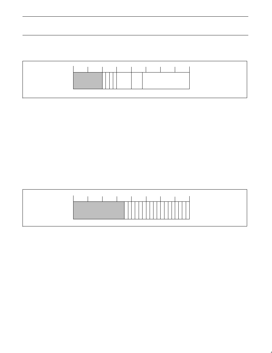
Philips Semiconductors
Preliminary specification
PDI1394L21
1394 full duplex AV link layer controller
1999 Aug 06
41
13.3
Asynchronous Control and Status Interface
13.3.1
Asynchronous RX/TX Control (ASYCTL) Base Address: 0x080
29 28 27 26 25 24 23 22 21 20 19 18 17 16 15 14 13 12 11 10 9 8 7 6 5 4 3 2 1 0
ARXALL
A
TXRST
ARXRST
SV00889
MAXRC
TOS
TOF
31 30
DIS_BCAST
Reset Value 0x00300320
Bit 23:
R/W
DIS_BCAST: Disable the reception of broadcast packets.
Bit 22:
R/W
ARXRST: Asynchronous receiver reset. This bit will auto clear when the link layer state machine is idle.
Bit 21:
R/W
ATXRST: Asynchronous transmitter reset
Bit 20:
R/W
ARXALL: Receive and filter only RESPONSE packets. When set (1), all responses are stored. When clear (0), only
solicited responses are stored.
Bit 19..16:
R/W
MAXRC: Maximum number of asynchronous transmitter single phase retries
Bit 15..13:
R/W
TOS: Time out seconds, integer of 1 second of the split transaction time out timer. Resets to "000". This timer is set
to the maximum amount of time the transmitter will wait for a pending response before the transmitter will begin
transmitting the next available request packet. Also see TOF bits of this timer.
Bit 12..0:
R/W
TOF: Time out fractions, integer of 1/8000 second. Resets to 0320h, which is 100 milliseconds. During the timeout of
the split transaction timer, subsequent split transactions are blocked. If it is desired to transmit multiple split
transactions this can be accomplished by following this procedure: (1) set the split transaction timer value to "0", (2)
disable the split timeout interrupt (TIMEOUT, bit 7 in register 0x0A0); (3) clear (set to "0") the unsolicited response
filter bit (ARXALL, bit 20 in register 0x080). Now use tLabels (transaction Labels, see section 12.5.1) to pair
transmitted packets with received packets. Use software timers to timeout the subsequent pending responses.
13.3.2
Asynchronous RX/TX Memory Status (ASYMEM) Base Address: 0x084
TREQQIDLE
RRSPQF
TREQQAF
TREQQ5A
V
29 28 27 26 25 24 23 22 21 20 19 18 17 16 15 14 13 12 11 10 9 8 7 6 5 4 3 2 1 0
TRSPQF
TRSPQAF
RREQQE
RREQQF
RREQQAF
RREQQ5A
V
RRSPQAF
RRSPQE
TRSPQ5A
V
RRSPQ5A
V
TREQQF
TRSPQE
TREQQE
31 30
SV00918
TRSPQIDLE
Reset Value 0x00033333
Unused bits read `0'. The information in this register is primarily used for diagnostics.
Bit 17:
R
TRSPQIDLE: Transmitter response queue is idle. Indicates that the transfer register for this queue is empty.
Bit 16:
R
TREQQIDLE: Transmitter request queue is idle. Indicates that the transfer register for this queue is empty.
Bit 15:
R
RRSPQF: Receiver response queue full.
Bit 14:
R
RRSPQAF: Receiver response queue almost full (precisely 1 more quadlet available).
Bit 13:
R
RRSPQ5AV: Receiver response queue at least 5 quadlets available.
Bit 12:
R
RRSPQE: Receiver response queue empty.
Bit 11:
R
RREQQF: Receiver request queue full.
Bit 10:
R
RREQQAF: Receiver request queue almost full (precisely 1 more quadlet available).
Bit 9:
R
RREQQ5AV: Receiver request queue at least 5 quadlets available.
Bit 8:
R
RREQQE: Receiver request queue empty.
Bit 7:
R
TRSPQF: Transmitter response queue full.
Bit 6:
R
TRSPQAF: Transmitter response queue almost full (precisely 1 more quadlet available).
Bit 5:
R
TRSPQ5AV: Transmitter response queue at least 5 quadlets available.
Bit 4:
R
TRSPQE: Transmitter response queue empty.
Bit 3:
R
TREQQF: Transmitter request queue full.
Bit 2:
R
TREQQAF: Transmitter request queue almost full (precisely 1 more quadlet available).
Bit 1:
R
TREQQ5AV: Transmitter request queue at least 5 quadlets available.
Bit 0:
R
TREQQE: Transmitter request queue empty.

Philips Semiconductors
Preliminary specification
PDI1394L21
1394 full duplex AV link layer controller
1999 Aug 06
42
13.3.3
Asynchronous Transmit Request Next (TX_RQ_NEXT) Base Address: 0x088
29 28 27 26 25 24 23 22 21 20 19 18 17 16 15 14 13 12 11 10 9 8 7 6 5 4 3 2 1 0
TX_RQ_NEXT
SV00293
31 30
Bit 31..0:
W
TX_RQ_NEXT: First/middle quadlet of packet for transmitter request queue (write only).
Writing this register will clear the TREQQWR flag until the quadlet has been written to its queue.
13.3.4
Asynchronous Transmit Request Last (TX_RQ_LAST) Base Address: 0x08C
29 28 27 26 25 24 23 22 21 20 19 18 17 16 15 14 13 12 11 10 9 8 7 6 5 4 3 2 1 0
TX_RQ_LAST
SV00294
3130
Bit 31..0:
W
TX_RQ_LAST: Last quadlet of packet for transmitter request queue (write only).
Writing this register will clear the TREQQWR flag until the quadlet has been written to its queue.
13.3.5
Asynchronous Transmit Response Next (TX_RP_NEXT) Base Address: 0x090
29 28 27 26 25 24 23 22 21 20 19 18 17 16 15 14 13 12 11 10 9 8 7 6 5 4 3 2 1 0
TX_RP_NEXT
SV00295
31 30
Bit 31..0:
W
TX_RP_NEXT: First/middle quadlet of packet for transmitter response queue (write only).
Writing this register will clear the TRSPQWR flag until the quadlet has been written to its queue.
13.3.6
Asynchronous Transmit Response Last (TX_RP_LAST) Base Address: 0x094
29 28 27 26 25 24 23 22 21 20 19 18 17 16 15 14 13 12 11 10 9 8 7 6 5 4 3 2 1 0
TX_RP_LAST
SV00296
3130
Bit 31..0:
W
TX_RP_LAST: Last quadlet of packet for transmitter response queue (write only).
Writing this register will clear the TRSPQWR flag until the quadlet has been written to its queue.
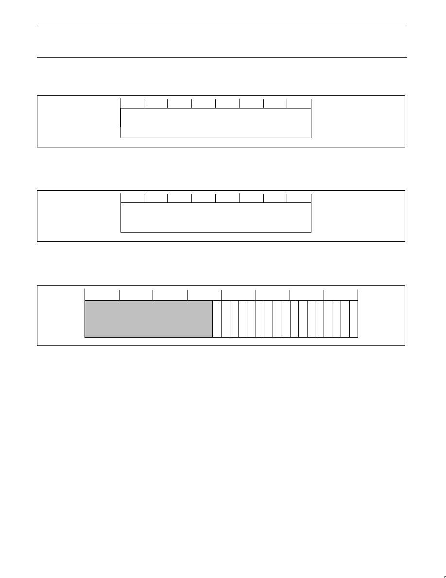
Philips Semiconductors
Preliminary specification
PDI1394L21
1394 full duplex AV link layer controller
1999 Aug 06
43
13.3.7
Asynchronous Receive Request (RREQ) Base Address: 0x098
29 28 27 26 25 24 23 22 21 20 19 18 17 16 15 14 13 12 11 10 9 8 7 6 5 4 3 2 1 0
RREQ
SV00297
3130
Reset Value 0x00000000
Bit 31..0:
R
RREQ:Quadlet of packet from receiver request queue (transfer register).
Reading this register will clear the RREQQQAV flag until the next received quadlet is available for reading.
13.3.8
Asynchronous Receive Response (RRSP) Base Address: 0x09C
29 28 27 26 25 24 23 22 21 20 19 18 17 16 15 14 13 12 11 10 9 8 7 6 5 4 3 2 1 0
RRSP
SV00298
31 30
Reset Value 0x00000000
Bit 31..0:
R
RRSP:Quadlet of packet from receiver response queue (transfer register).
Reading this register will clear the RRSPQQAV flag until the next received quadlet is available for reading.
13.3.9
Asynchronous RX/TX Interrupt Acknowledge (ASYINTACK) Base Address: 0x0A0
SV01077
29 28
27 26 25 24 23
22 21 20 19 18
17 16
15 14 13
12 11 10
9
8
7
6
5
4
3
2
1
0
TIMEOUT
RCVDRSP
RRSPQFULL
RREQQFULL
RREQQQA
V
RRSPQRDERR
RREQQRDERR
RRSPQQA
V
SIDQA
V
RREQQLASTQ
TRSPQFULL
RRSPQLASTQ
TREQQWRERR
TRSPQWR
TRSPQWRERR
TREQQFULL
TREQQWR
31 30
Reset Value 0x00000C00
Bit 31..17:
R/W
Unused bits read `0'
Bit 16:
R/W
RRSPQFULL: Receiver response queue did become full. Write a "1" to this bit to reset the interrupt.
Bit 15:
R/W
RREQQFULL: Receiver request queue did become full. Write a "1" to this bit to reset the interrupt.
Bit 14:
R/W
SIDQAV: Current quadlet in RREQ is self ID data. This bit is set only after a bus reset, not after reception of PHY
packets other than self IDs. This interrupt automatically resets when the quadlet is read.
Bit 13:
R/W
RRSPQLASTQ: Current quadlet in RRSP is last quadlet of packet. This interrupt automatically resets when the
quadlet is read.
Bit 12:
R/W
RREQQLASTQ: Current quadlet in RREQ is last quadlet of packet. This interrupt automatically resets when the
quadlet is read.
Bit 11:
R/W
RRSPQRDERR: Receiver response queue read error (transfer error) or bus reset occurred.
When set (1), this queue is blocked for read access. Write a "1" to this bit to reset the interrupt.
Bit 10:
R/W
RREQQRDERR: Receiver request queue read error (transfer error) or bus reset occurred.
When set (1), this queue is blocked for read access. Write a "1" to this bit to reset the interrupt.
Bit 9:
R/W
RRSPQQAV: Receiver response queue quadlet available (in RRSP). This interrupt automatically resets when the
quadlet is read.
Bit 8:
R/W
RREQQQAV: Receiver request queue quadlet available (in RREQ). This interrupt automatically resets when the
quadlet is read.
Bit 7:
R/W
TIMEOUT: Split transaction response timeout. Write a "1" to this bit to reset the interrupt.
Bit 6:
R/W
RCVDRSP: Solicited response received (within timeout interval). Write a "1" to this bit to reset the interrupt.
Bit 5:
R/W
TRSPQFULL: Transmitter response queue did become full. Write a "1" to this bit to reset the interrupt.
Bit 4:
R/W
TREQQFULL: Transmitter request queue did become full. Write a "1" to this bit to reset the interrupt.
Bit 3:
R/W
TRSPQWRERR: Transmitter response queue write error (transfer error). Write a "1" to this bit to reset the interrupt.
Bit 2:
R/W
TREQQWRERR: Transmitter request queue write error (transfer error). Write a "1" to this bit to reset the interrupt.
Bit 1:
R/W
TRSPQWR: Transmitter response queue written (transfer register emptied). Write a "1" to this bit to reset the interrupt.
Philips Semiconductors
Preliminary specification
PDI1394L21
1394 full duplex AV link layer controller
1999 Aug 06
44
Bit 0:
R/W
TREQQWR: Transmitter request queue written (transfer register emptied). Write a "1" to this bit to reset the interrupt.
13.3.10
Asynchronous RX/TX Interrupt Enable (ASYINTE) Base Address: 0x0A4
29 28
27 26 25 24 23
22 21 20 19 18
17 16
15 14 13
12 11 10
9
8
7
6
5
4
3
2
1
0
ETIMEOUT
ERCVDRSP
ERRSPQFULL
ERREQQFULL
ERREQQQA
V
ERRSPQRDERR
ERREQQRDERR
ERRSPQQA
V
ESIDQA
V
ERREQQLASTQ
ETRSPQFULL
ERRSPQLASTQ
ETREQQWRERR
ETRSPQWR
ETRSPQWRERR
ETREQQFULL
ETREQQWR
31 30
SV00797
Reset Value 0x00000000
Bits16..0 are interrupt enable bits for the Asynchronous RX/TX Interrupt Acknowledge (ASYINTACK).
14.0
DC ELECTRICAL CHARACTERISTICS
Table 10.
DC Electrical Characteristics
SYMBOL
PARAMETER
MIN
MAX
UNIT
NOTE
V
IL
LOW input voltage
0.8
V
Pin categories 1, 2, 3
V
IH
HIGH input voltage
2.0
V
Pin categories 1, 2, 3
V
IT1
+
Input threshold, rising edge
V
DD
/2 + 0.3
V
DD
/2 + 0.9
V
Pin categories 6, 8
LOW to HIGH transition
V
IT1
Input threshold, falling edge
V
DD
/2 0.9
V
DD
/2 0.3
V
Pin categories 6, 8
HIGH to LOW transition
V
OH1
HIGH output voltage
2.4
V
Pin category 1
I
OH
= 8mA
I
OL
= 8mA
V
OL1
LOW output voltage
0.4
V
Pin category 1
I
OH
= 8mA
I
OL
= 8mA
V
OH2
HIGH output voltage
2.4
V
Pin categories 4, 6, 7
I
OH
= 4mA
V
OL2
LOW output voltage
0.4
V
Pin categories 4, 5, 6, 7
I
OL
= 4mA
I
Input leakage current
±
1
m
A
Pin categories 1, 2, 3
V
I
= 5.5V or 0V
I
L
Input leakage current
200
m
A
Pin category 8
V
I
= 5.5V or 0V
I
O
3 State output current
±
5
m
A
Pin categories 1, 7
V
I
= 5.5V or 0V
I
OZ
3-State output current
200
m
A
Pin category 6
V
I
= 5.5V or 0V
I
DD
Active supply current
75
mA
Under idle conditions, the average
value is 15 mA

Philips Semiconductors
Preliminary specification
PDI1394L21
1394 full duplex AV link layer controller
1999 Aug 06
45
14.1
Pin Categories
Table 11.
Pin Categories
Category 1:
Input/Output
Category 2:
Input
Category 3:
Input
Category 4:
Output
Category 5:
Output
Category 6:
Input/Output
Category 7:
Category 8:
HIF D[7:0]
HIF A[8:0]
RESET_N
CYCLEOUT
HIF INT_N
PHY D[0:7]
LREQ
SCLK
AVxSYNC
HIF CS_N
CYCLEIN
AVxERR0
PHY CTL[0:1]
AVxVALID
HIF WR_N
ISO_N
AVxERR1
AV xD[7:0]
HIF RD_N
CLK25
AVxENKEY
AVxENDPCK
AVxCLK
AVxFSYNC
15.0
AC CHARACTERISTICS
GND = 0V, C
L
= 50pF
LIMITS
SYMBOL
PARAMETER
TEST CONDITIONS
WAVEFORMS
T
amb
= 0
°
C to +70
°
C
UNIT
MIN
TYP
MAX
t
PERIOD
AV clock period
Figure 26
41.67
ns
t
SU
AV clock setup time
Figure 26
20
ns
t
IH
AV clock input hold time
Figure 26
3
ns
t
OD
AV clock output delay time
Figure 26
3
24
ns
t
WHIGH
AV clock pulse width HIGH
Figure 26
10
t
WLOW
AV clock pulse width LOW
Figure 26
10
t
PWFS
AVxFSYNC pulse width HIGH
Figure 27
100
140
ns
t
SUP
PHY-link setup time
Figure 28
6.0
ns
t
HP
PHY-link hold time
Figure 28
0
ns
t
SCLKPER
SCLK period
Figure 28
20.343
20.345
20.347
ns
t
DP
PHY-link output delay
Note: C
L
= 20pF
Figure 29
2.0
10.0
ns
t
AS
Host address setup time
Figure 30
0
ns
t
AH
Host address hold time
Figure 30
0
ns
t
CL
Host chip select pulse width LOW
Figure 30
115
ns
t
CH
Host chip select pulse width HIGH
Figure 30
42
ns
t
RP
Host read pulse width
Figure 30
115
ns
t
ACC
Host access time
Figure 30
115
ns
t
DH
Host data hold time
Figure 30
0
ns
t
DS
Host data setup time
Figure 30
0
ns
t
DZ
Host data bus release (Hi-Z)
Figure 30
15
ns
t
WRP
Host write pulse width
Figure 30
115
ns
t
CWH
CYCLEIN HIGH pulse width
Figure 31
200
ns
t
CWL
CYCLEIN LOW pulse width
Figure 31
200
ns
t
CP
CYCLEIN cycle period
Figure 31
125
µ
s
t
CD
CYCLEOUT cycle delay
Figure 32
20
ns
t
RESET
RESET_N pulse width LOW
Figure 33
10
µ
s
Philips Semiconductors
Preliminary specification
PDI1394L21
1394 full duplex AV link layer controller
1999 Aug 06
46
16.0
TIMING DIAGRAMS
16.1
AV Interface Operation
SV00240
AVCLK
AV D[7:0]
MESSAGE
INVALID DATA
MESSAGE
MESSAGE
INVALID DATA
AVSYNC
AVVALID
AVERR[0]
AVERR[1]
ASSERTED IN THE EVENT OF A BUS PACKET CRC ERROR
ASSERTED IN THE EVENT OF A DATA BLOCK SEQUENCE ERROR
Figure 25. AV Interface Operation Diagram
16.2
AV Interface Critical Timings
SV00688
tWHIGH
tWLOW
tPERIOD
ÉÉÉ
ÉÉÉ
ÉÉÉ
ÉÉÉ
tSU
tIH
tOD
AVCLK
AV D [7:0], AVVALID,
AVSYNC, AVENDPCK
VALID
VALID
AV D [7:0], AVERR[1:0],
AVSYNC, AVVALID
Figure 26. AV Interface Timing Diagram
SV00890
tPWFS
AVxFSYNC
Figure 27. AVxFSYNC Timing Diagram
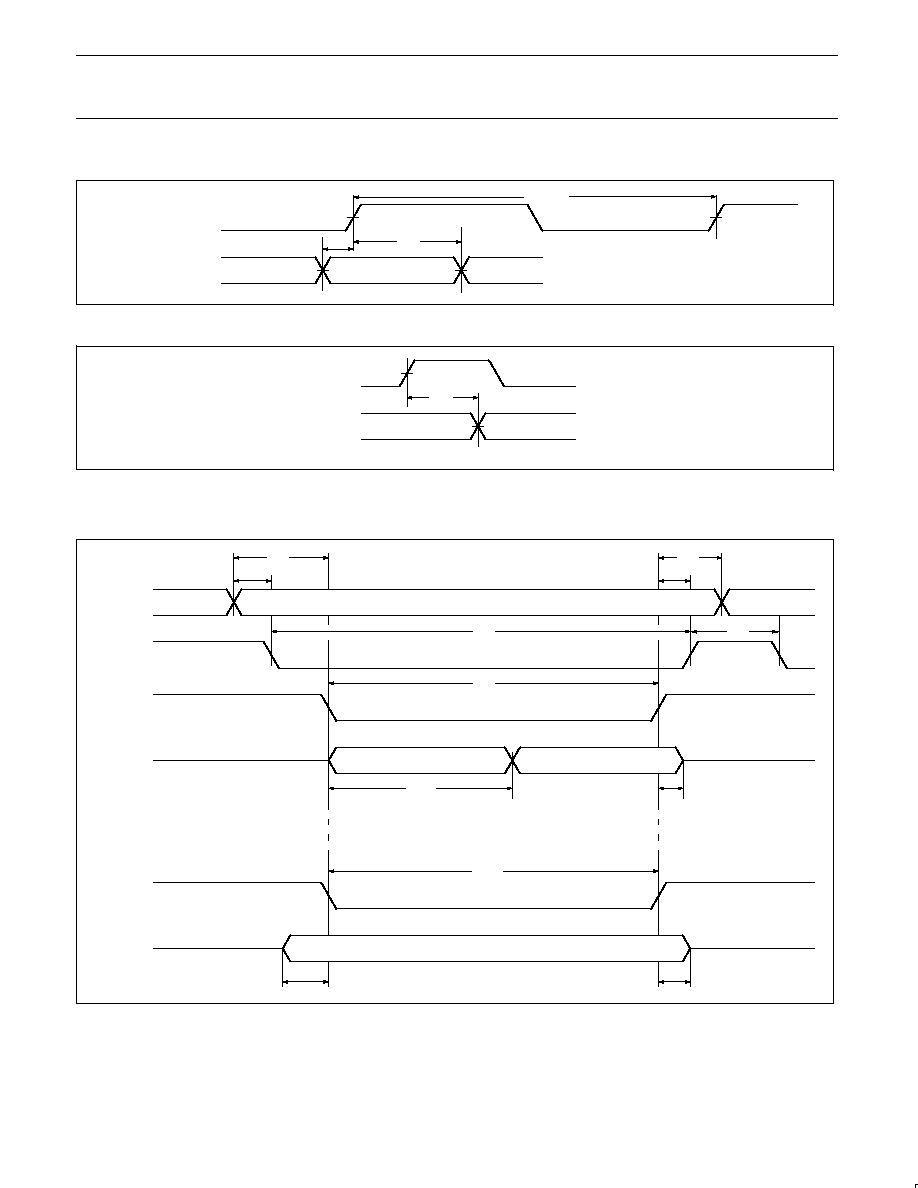
Philips Semiconductors
Preliminary specification
PDI1394L21
1394 full duplex AV link layer controller
1999 Aug 06
47
16.3
PHY-Link Interface Critical Timings
t
HP
t
SUP
SCLK
PHY D[0:7], PHY CTL[0:1]
50%
50%
50%
SV00919
t
SCLKPER
50%
Figure 28. PHY D[0:7], PHY CTL[0:1] Input Setup and Hold Timing Waveforms
t
DP
SCLK
PHY D[0:7], PHY CTL[0:1], LREQ
50%
50%
SV00694
Figure 29. PHY D[0:7], PHY CTL[0:1], and LREQ Output-Delay Timing Waveforms
16.4
Host Interface Critical Timings
SV00920
t
ACC
t
AS
HIF A[8:0]
ÉÉÉÉÉÉÉÉÉ
ÉÉÉÉÉÉÉÉÉ
t
AH
t
AS
t
AH
VALID
VALID
t
DZ
t
CL
t
RP
t
WRP
READ
WRITE
t
DH
HIF CS_N
HIF RD_N
HIF D[7:0]
t
DS
HIF WR_N
HIF D[7:0]
VALID
t
CH
Figure 30. Host Interface Timing Waveforms

Philips Semiconductors
Preliminary specification
PDI1394L21
1394 full duplex AV link layer controller
1999 Aug 06
48
16.5
CYCLEIN/CYCLEOUT Timings
SV00696
50%
50%
50%
tCWH
tCWL
CYCLEIN
tCP
Figure 31. CYCLEIN Waveform
SV00697
tCD
50%
50%
50%
50%
tCD
SCLK
CYCLEIN
CYCLEOUT
Figure 32. CYCLEOUT Waveforms
16.6
RESET Timings
tRESET
50%
50%
SV00698
RESET_N
Figure 33. RESET_N Waveform
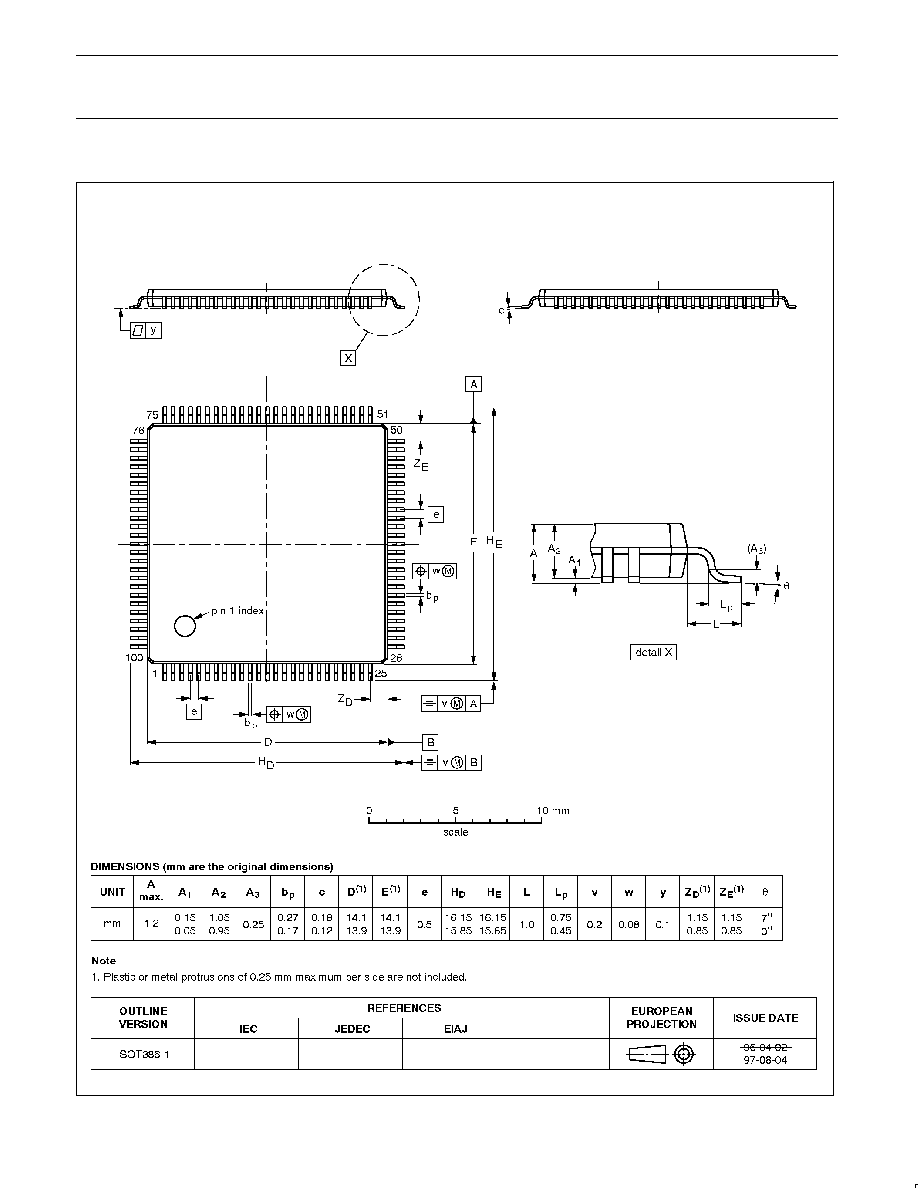
Philips Semiconductors
Preliminary specification
PDI1394L21
1394 full duplex AV link layer controller
1999 Aug 06
49
TQFP100:
plastic thin quad flat package; 100 leads; body 14 x 14 x 1.0 mm
SOT386-1

Philips Semiconductors
Preliminary specification
PDI1394L21
1394 full duplex AV link layer controller
1999 Aug 06
50
LQFP100:
plastic low profile quad flat package; 100 leads; body 14 x 14 x 1.4 mm
SOT407-1

ERRATA LIST FOR THE PHILIPS
PDI1394L21 1394 FULL DUPLEX AV LINK LAYER CONTROLLER
(These errata refer to the data sheet dated 1999 August 6)
Philips Semiconductors
Errata To the PDI1394L21 1394 Full Duplex AV Link Layer Controller (Data Sheet dated: 1999 August 6).
August 6, 1999
Chip Errata:
E-1. Self-ID Packet Issues:
Description of expected operation: After bus reset, the queues are flushed and a self-ID packet should be
placed in the Read Request Queue. Refer to section 12.5.2.4 (Self-ID and PHY packets receive) in the
"PDI1394L21 1394 Full Duplex AV Link Layer Controller" data sheet for the proper format of a self-ID packet.
Description of observed behavior: Occasionally 0x000000E0 and 0x00000010 quadlets are found in the Read
Request Queue with no accompanying self-ID and acknowledge quadlet. This type of self-ID is valid ONLY for a
node which is not connected to any other node (node standing alone). This partial self-ID packet results from a
recent node connection (hot plug) event or Link/PHY hardware reset.
Solution or work around: Issue a software bus reset and read the self IDs generated by that reset.
E-2. AVFSYNC pin function at high FSYNC pulse repetition rates:
Description of expected operation: With the EN_FS bits set on the isochronous transmitter of the transmitting
node and the isochronous receiver of the receiving node, a pulse introduced at the FSYNC pin on the transmitting
AV port of the transmitting node will produce an SYT field time stamp in the next bus packet which will, in turn,
produce a pulse at the FSYNC pin of the receiving AV port on the receiving node at a time corresponding to the
expiration of the SYT field time stamp, with the SYT Delay introduced at the transmitter taken into account.
Description of observed behavior: At rep rates below 2 KHz, the system works as expected. At rep rates
greater than 2 KHz (dependant upon the setting of the SYT Delay bits) the system operates as expected for a
short period of time (about 100 milliseconds), then operates erratically thereafter.
Solution or work around: Do not use above the following rep rates with the corresponding SYT Delay settings:
SYT Delay = 2 bus cycles, maximum rep rate = 3,200; SYT Delay = 3 bus cycles, maximum rep rate = 3,200;
SYT Delay = 4 bus cycles, maximum rep rate = 4,200.
E-3. AVENKEY pin function:
Description of expected operation: This pin / function is intended to attach a specific "key" state to each byte of
a transmitted isochronous packet by means of reading the ENKEY pin on the transmitting AV port while the first
byte of an application packet is being inputted. The ENKEY state of the first inputted byte is the state of all packet
bytes.
Description of observed behavior: Unless the state of the ENKEY pin is inputted within a certain part of the link
internal clock cycle, occasionally some of the bytes in a packet are keyed with the wrong state. This results in
packets getting "stuck" in the isochronous transmit FIFO and causing FIFO overfill.
Solution or work around: Input key states only with reference to the CLK25 signal of the link chip to assure
proper synchronization. The AVCLK signal must rise 8 to 41 nS before the CLK25 signal rises for proper
operation at 12.288 MHz. It is the AVCLK signal which introduces the state of the ENKEY pin (and all
others) to the AV port interface logic. Please consult Philips IEEE 1394 Applications Engineering Group
(1394@philips.com) for use of this function at other AVCLK frequencies.

Philips Semiconductors
Preliminary specification
PDI1394L21
1394 full duplex AV link layer controller
1999 Aug 06
52
Definitions
Short-form specification -- The data in a short-form specification is extracted from a full data sheet with the same type number and title. For
detailed information see the relevant data sheet or data handbook.
Limiting values definition -- Limiting values given are in accordance with the Absolute Maximum Rating System (IEC 134). Stress above one
or more of the limiting values may cause permanent damage to the device. These are stress ratings only and operation of the device at these or
at any other conditions above those given in the Characteristics sections of the specification is not implied. Exposure to limiting values for extended
periods may affect device reliability.
Application information -- Applications that are described herein for any of these products are for illustrative purposes only. Philips
Semiconductors make no representation or warranty that such applications will be suitable for the specified use without further testing or
modification.
Disclaimers
Life support -- These products are not designed for use in life support appliances, devices or systems where malfunction of these products can
reasonably be expected to result in personal injury. Philips Semiconductors customers using or selling these products for use in such applications
do so at their own risk and agree to fully indemnify Philips Semiconductors for any damages resulting from such application.
Right to make changes -- Philips Semiconductors reserves the right to make changes, without notice, in the products, including circuits, standard
cells, and/or software, described or contained herein in order to improve design and/or performance. Philips Semiconductors assumes no
responsibility or liability for the use of any of these products, conveys no license or title under any patent, copyright, or mask work right to these
products, and makes no representations or warranties that these products are free from patent, copyright, or mask work right infringement, unless
otherwise specified.
Philips Semiconductors
811 East Arques Avenue
P.O. Box 3409
Sunnyvale, California 940883409
Telephone 800-234-7381
©
Copyright Philips Electronics North America Corporation 1999
All rights reserved. Printed in U.S.A.
Date of release: 08-99
Document order number:
9397 750 05512
Philips
Semiconductors
Data sheet
status
Objective
specification
Preliminary
specification
Product
specification
Product
status
Development
Qualification
Production
Definition
[1]
This data sheet contains the design target or goal specifications for product development.
Specification may change in any manner without notice.
This data sheet contains preliminary data, and supplementary data will be published at a later date.
Philips Semiconductors reserves the right to make changes at any time without notice in order to
improve design and supply the best possible product.
This data sheet contains final specifications. Philips Semiconductors reserves the right to make
changes at any time without notice in order to improve design and supply the best possible product.
Data sheet status
[1]
Please consult the most recently issued datasheet before initiating or completing a design.