Document Outline
- FEATURES
- DESCRIPTION
- PIN CONFIGURATION
- ORDERING INFORMATION
- PIN DESCRIPTION
- FUNCTION TABLE
- BLOCK DIAGRAM
- ABSOLUTE MAXIMUM RATINGS 1
- RECOMMENDED OPERATING CONDITIONS 1
- DC ELECTRICAL CHARACTERISTICS
- TIMING REQUIREMENTS
- AC CHARACTERISTICS
- AC WAVEFORMS
- TEST CIRCUIT
- PACKAGE OUTLINE
- REVISION HISTORY
- Data sheet status
- Definitions
- Disclaimers

Philips
Semiconductors
PCKV857A
100-250 MHz differential
1:10 clock driver
Product data
Supersedes data of 2002 Dec 13
2003 Jul 31
INTEGRATED CIRCUITS
Philips Semiconductors
Product data
PCKV857A
100-250 MHz differential 1:10 clock driver
2
2003 Jul 31
FEATURES
·
ESD classification testing is done to JEDEC Standard JESD22.
Protection exceeds 2000 V to HBM per method A114.
·
Latch-up testing is done to JEDEC Standard JESD78 which
exceeds 100 mA
·
Optimized for clock distribution in DDR (Double Data Rate)
SDRAM applications as per JEDEC specifications
·
1-to-10 differential clock distribution
·
Very low skew (
<
100 ps) and jitter (
<
100 ps)
·
Operation from 2.2 V to 2.7 V AV
DD
and 2.3 V to 2.7 V V
DD
·
SSTL_2 interface clock inputs and outputs
·
CMOS control signal input
·
Test mode enables buffers while disabling PLL
·
Low current power-down mode
·
Tolerant of Spread Spectrum input clock
·
Full DDR solution provided when used with SSTL16877 or
SSTV16857
·
Designed for DDR 266, 300, and 333 DIMM applications
·
Available in TSSOP-48 and TVSOP-48 packages
DESCRIPTION
The PCKV857A is a high-performance, low-skew, low-jitter zero
delay buffer designed for 2.5 V V
DD
and 2.5 V AV
DD
operation and
differential data input and output levels.
The PCKV857A is a zero delay buffer that distributes a differential
clock input pair (CLK, CLK) to ten differential pairs of clock outputs
(Y[0:9], Y[0:9]) and one differential pair feedback clock outputs
(FB
OUT
, FB
OUT
) . The clock outputs are controlled by the clock
inputs (CLK, CLK), the feedback clocks (FB
IN
, FB
IN
), and the analog
power input (AV
DD
). When PWRDWN is HIGH, the outputs switch in
phase and frequency with CLK. When PWRDWN is LOW, all
outputs are disabled to HIGH impedance state (3-State), and the
PLL is shut down (LOW power mode). The device also enters the
LOW power mode when the input frequency falls below 20 MHz. An
input frequency detection circuit will detect the LOW frequency
condition and after applying a > 20 MHz input signal, the detection
circuit turns on the PLL again and enables the outputs.
When AV
DD
is grounded, the PLL is turned off and bypassed for test
purposes. The PCKV857A is also able to track spread spectrum
clocking for reduced EMI.
The PCKV857A is characterized for operation from 0 to +70
°
C.
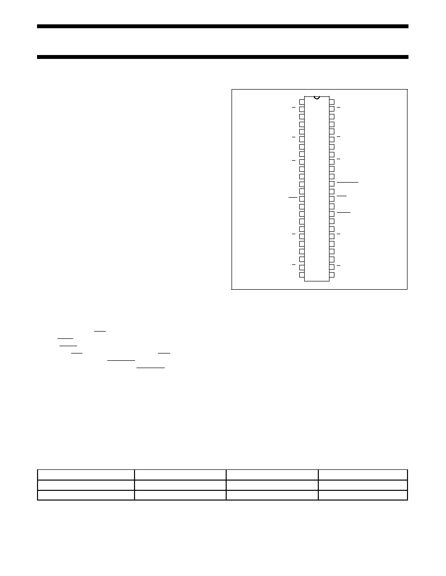
PIN CONFIGURATION
1
2
3
4
5
6
7
8
9
10
11
12
13
14
15
16
17
18
19
20
25
26
27
28
29
30
31
32
33
34
35
36
37
38
39
40
21
22
23
24
41
42
43
44
45
46
47
48
GND
Y
0
Y
0
V
DDQ
Y
1
Y
1
GND
Y
2
GND
Y
2
V
DDQ
V
DDQ
CLK
CLK
V
DDQ
AV
DD
AGND
GND
Y
3
Y
3
V
DDQ
Y
4
Y
4
GND
GND
Y
5
Y
5
V
DDQ
Y
6
Y
6
GND
GND
Y
7
Y
7
V
DDQ
PWRDWN
FB
IN
FB
IN
V
DDQ
FB
OUT
FB
OUT
GND
Y
8
Y
8
V
DDQ
Y
9
Y
9
SW00691
GND
ORDERING INFORMATION
PACKAGES
TEMPERATURE RANGE
ORDER CODE
DRAWING NUMBER
48-Pin Plastic TSSOP
0 to +70
°
C
PCKV857ADGG
SOT362-1
48-Pin Plastic TSSOP (TVSOP)
0 to +70
°
C
PCKV857ADGV
SOT480-1

Philips Semiconductors
Product data
PCKV857A
100-250 MHz differential 1:10 clock driver
2003 Jul 31
3
PIN DESCRIPTION
PINS
SYMBOL
DESCRIPTION
1, 7, 8, 18, 24, 25, 31, 41, 42, 48
GND
SSTL_2 ground pins
2, 3, 5, 6, 9, 10, 19, 20, 22, 23, 26, 27, 29,
30, 32, 33, 39, 40, 43, 44, 46, 47
Y
n
, Y
n
, FB
OUT
, FB
OUT
SSTL_2 differential outputs
4, 11, 12, 15, 21, 28, 34, 38, 46
V
DDQ
SSTL_2 power pins
13, 14, 35, 36
CLK
IN
, CLK
IN
, FB
IN
, FB
IN
SSTL_2 differential inputs
16
AV
DD
Analog power
17
AGND
Analog ground
37
PWRDWN
Power-down control input
FUNCTION TABLE
INPUTS
OUTPUTS
PWRDWN
CLK
CLK
Y
n
Y
n
FB
OUT
FB
OUT
PLL ON/OFF
L
L
H
Z
Z
Z
1
Z
1
OFF
L
H
L
Z
Z
Z
1
Z
1
OFF
H
L
H
L
H
L
H
ON
H
H
L
H
L
H
L
ON
X
2
<
20 MHz
<
20 MHz
Z
Z
Z
1
Z
1
OFF
NOTES:
H = HIGH voltage level
L = LOW voltage level
Z = HIGH impedance OFF-state
X = don't care
1. Subject to change. May cause conflict with FB
IN
pins.
2. Additional feature that senses when the clock input is less than 20 MHz and places the part in sleep mode.
BLOCK DIAGRAM
PLL
37 - PWRDWN
13 - CLK
14 - CLK
36 - FB
IN
35 - FB
IN
16 - AV
DD
3 - Y
0
2 - Y
0
5 - Y
1
6 - Y
1
10 - Y
2
9 - Y
2
20 - Y
3
19 - Y
3
22 - Y
4
23 - Y
4
46 - Y
5
47 - Y
5
44 - Y
6
43 - Y
6
39 - Y
7
40 - Y
7
29 - Y
8
30 - Y
8
27 - Y
9
28 - Y
9
32 - FB
OUT
33 - FB
OUT
SW00692
Philips Semiconductors
Product data
PCKV857A
100-250 MHz differential 1:10 clock driver
2003 Jul 31
4
ABSOLUTE MAXIMUM RATINGS
1
LIMITS
SYMBOL
PARAMETER
CONDITION
MIN
MAX
UNIT
V
DDQ
Supply voltage range
0.5
3.6
V
AV
DD
Supply voltage range
0.5
3.6
V
V
I
Input voltage range
see Notes 2 and 3
-0.5
V
DDQ
+
0.5
V
V
O
Output voltage range
see Notes 2 and 3
-0.5
V
DDQ
+
0.5
V
I
IK
Input clamp current
V
I
< 0 or V
I
>V
DDQ
--
±
50
mA
I
OK
Output clamp current
V
O
< 0 or V
O
>V
DDQ
--
±
50
mA
I
O
Continuous output current
V
O
= 0 to V
DDQ
--
±
50
mA
Continuous current to GND or V
DDQ
--
±
100
mA
T
stg
Storage temperature range
-65
+
150
°
C
NOTES:
1. Stresses beyond those listed under "absolute maximum ratings" may cause permanent damage to the device. These are stress ratings
only, and functional operation of the device at these or any other conditions beyond those indicated under "recommended operating
conditions" is not implied. Exposure to absolute-maximum-rated conditions for extended periods may affect device reliability.
2. The input and output negative voltage ratings may be exceeded if the input and output clamp-current ratings are observed.
3. This value is limited to 3.6 V maximum.
RECOMMENDED OPERATING CONDITIONS
1
LIMITS
SYMBOL
PARAMETER
CONDITION
MIN
TYP
MAX
UNIT
V
DDQ
Supply voltage range
2.3
--
2.7
V
AV
DD
Supply voltage range
2.2
--
2.7
V
V
LOW-level input voltage
CLK, CLK,
FB
IN
, FB
IN
--
--
V
DDQ
/2
-
0.18
V
V
IL
LOW-level input voltage
PWRDWN
-
0.3
--
0.7
V
V
HIGH-level input voltage
CLK, CLK,
FB
IN
, FB
IN
V
DDQ
/2
+
0.18
--
--
V
V
IH
HIGH-level input voltage
PWRDWN
1.7
--
V
DDQ
+
0.3
V
DC input signal voltage
Note 2
-
0.3
--
V
DDQ
V
DC differential input signal voltage
CLK, FB
IN
Note 3
0.36
--
V
DDQ
+
0.6
V
V
ID
AC differential input signal voltage
CLK, FB
IN
Note 3
0.7
--
V
DDQ
+
0.6
V
V
OX
Output differential cross-voltage
Note 4
V
DDQ
/2
-
0.2
V
DDQ
/2
V
DDQ
/2
+
0.2
V
V
IX
Input differential cross-voltage
Note 4
V
DDQ
/2
-
0.2
--
V
DDQ
/2
+
0.2
V
I
OH
HIGH-level output current
--
--
-
12
mA
I
OL
LOW-level output current
--
--
12
mA
SR
Input slew rate
1
--
4
V/ns
T
amb
Operating free-air temperature
0
--
70
°
C
NOTES:
1. Unused inputs must be held HIGH or LOW to prevent them from floating.
2. DC input signal voltage specifies the allowable DC execution of differential input.
3. Differential input signal voltage specifies the differential voltage |VTR - VCP| required for switching, where VTR is the true input level and
VCP is the complementary input level.
4. Differential cross-point voltage is expected to track variations of V
CC
and is the voltage at which the differential signals must be crossing.
Philips Semiconductors
Product data
PCKV857A
100-250 MHz differential 1:10 clock driver
2003 Jul 31
5
DC ELECTRICAL CHARACTERISTICS
Over recommended operating conditions. Voltages are referenced to GND (ground = 0 V).
LIMITS
SYMBOL
PARAMETER
TEST CONDITIONS
MIN
TYP
MAX
UNIT
V
IK
Input voltage, all inputs
V
DDQ
= 2.3 V, I
I
= -18 mA
--
--
-
1.2
V
V
DDQ
= min to max, I
OH
= -1 mA
V
DDQ
-
0.1
--
--
V
V
OH
HIGH-level output voltage
V
DDQ
= 2.3 V, I
OH
= -12 mA
1.7
--
--
V
V
DDQ
= min to max, I
OL
= 1 mA
--
--
0.1
V
V
OL
LOW-level output voltage
V
DDQ
= 2.3 V, I
OL
= 12 mA
--
--
0.6
V
I
I
Input current
V
DDQ
= 2.7 V, V
I
= 0 V to 2.7 V
--
--
±
10
µ
A
I
OZ
HIGH-impedance-state output current
V
DDQ
= 2.7 V, V
O
= V
DDQ
or GND
--
--
±
10
µ
A
I
DDPD
Power-down current on V
DDQ
+ AV
DD
CLK and CLK = 0 MHz,
PWRDWN = LOW;
of I
DD
and AI
DD
--
30
100
µ
A
I
DD
Dynamic current on V
DDQ
f
O
= 67 MHz to 190 MHz
--
200
300
mA
AI
DD
Supply current on AV
DD
f
O
= 67 MHz to 190 MHz
--
8
10
mA
C
I
Input capacitance
V
CC
= 2.5 V, V
I
= V
CC
or GND
2
2.8
3
pF
NOTE:
1. This is intended to operate in the SSTL_2 type IV unterminated mode without series resistors on the outputs.
2. All typical values are at respective nominal V
DDQ
.
3. Differential cross-point voltage is expected to track variations of V
DDQ
and is the voltage at which the differential signals must be crossing.
TIMING REQUIREMENTS
Over recommended ranges of supply voltage and operating free-air temperature.
SYMBOL
PARAMETER
MIN
MAX
UNIT
f
CK
Operating clock frequency
100
250
MHz
Input clock duty cycle
40
60
%
Stabilization time
1
100
--
µ
s
NOTE:
1. Time required for the integrated PLL circuit to obtain phase lock of its feedback signal to its reference signal after power-up.
Philips Semiconductors
Product data
PCKV857A
100-250 MHz differential 1:10 clock driver
2003 Jul 31
6
AC CHARACTERISTICS
GND = 0 V; t
r
= t
f
2.5 ns; C
L
= 50 pF; R
L
= 1 k
LIMITS
SYMBOL
PARAMETER
WAVEFORM
CONDITION
MIN
TYP
MAX
UNIT
t
(O)
Static phase offset
Figure 1
-350
0
350
ps
t
SK(O)
Output clock skew
Figure 2
--
--
150
ps
t
SLR(O)
Output clock slew rate
Figure 3
1
--
2
V/ns
t
JIT(PER)
Jitter (period)
Figure 4
f
O
= 67 MHz to 200 MHz
-75
--
75
ps
t
JIT(CC)
Jitter (cycle-to-cycle)
Figure 5
f
O
= 67 MHz to 200 MHz
-75
--
75
ps
t
JIT(HPER)
Half-period jitter
Figure 6
-75
--
75
ps
t
PLH
1
LOW to HIGH level
propagation delay
Test mode/CLK to any
output
--
3.7
--
ns
t
PHL
1
HIGH to LOW level
propagation delay
Test mode/CLK to any
output
--
3.7
--
ns
NOTE:
1. Refers to transition of noninverting output.
The PLL clock distribution device and SSTL registered drivers reduce
signal loads on the memory controller and prevent timing delays and
waveform distortions that would cause unreliable operation
SW00945
SDRAM
SDRAM
SDRAM
SDRAM
SDRAM
SDRAM
SDRAM
SDRAM
SDRAM
SSTL16877
or
SSTV16857
PCKV857A
FRONT SIDE
SSTL16877
or
SSTV16857
Philips Semiconductors
Product data
PCKV857A
100-250 MHz differential 1:10 clock driver
2003 Jul 31
7
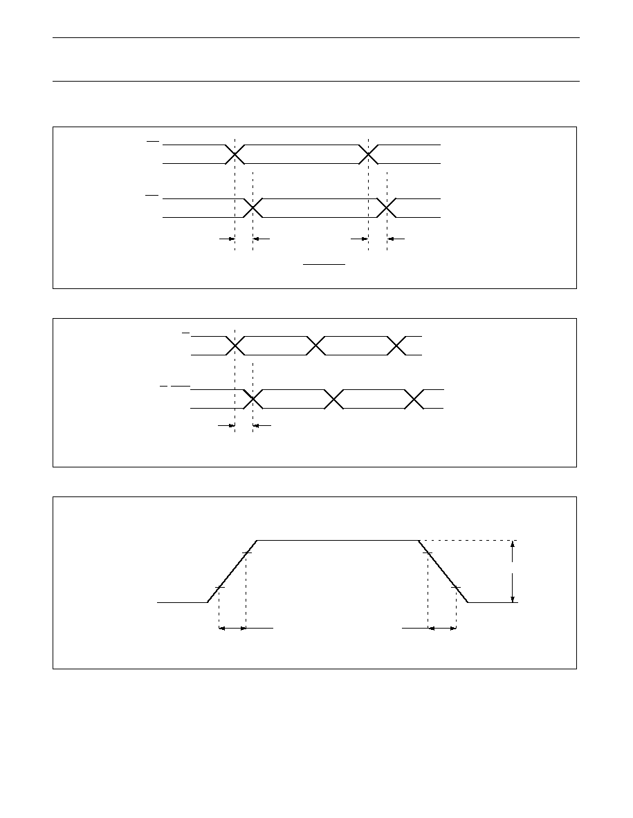
AC WAVEFORMS
SW00882
t
(O)
=
1
n =N
t
(O)n
N
t
(O)n
t
(O)n + 1
(N is a large number of samples)
CLK
CLK
FB
IN
FB
IN
Figure 1. Static phase offset
SW00883
t
sk(O)
Yx
Yx
Yx, FB
OUT
Yx, FB
OUT
Figure 2. Output skew
80%
80%
20%
20%
CLOCK INPUTS
AND OUTPUTS
t
SLR(I)
, t
SLR(O)
t
SLR(I)
, t
SLR(O)
V
ID
, V
OD
SW00886
Figure 3. Input and output slew rates
Philips Semiconductors
Product data
PCKV857A
100-250 MHz differential 1:10 clock driver
2003 Jul 31
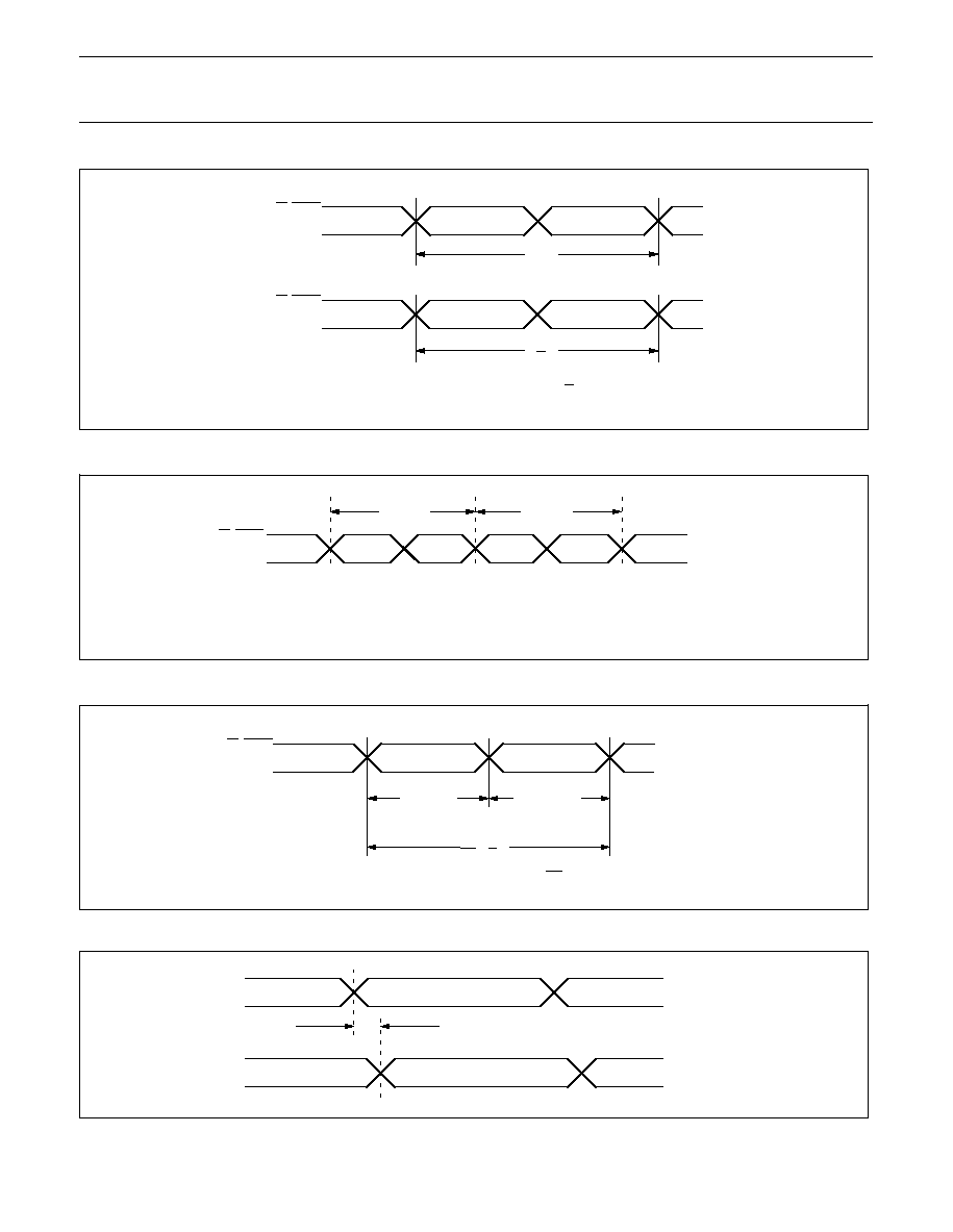
8
f
O
Yx, FB
OUT
Yx, FB
OUT
t
cycle n
Yx, FB
OUT
Yx, FB
OUT
1
t
JIT(PER)
= t
cycle n
-
f
O
1
SW00884
Figure 4. Period jitter
t
cycle n
t
cycle n + 1
SW00881
t
JIT(CC)
= t
cycle n
- t
cycle n+1
Yx, FB
OUT
Yx, FB
OUT
Figure 5. Cycle-to-cycle jitter
f
O
Yx, FB
OUT
Yx, FB
OUT
t
half period n
1
t
JIT(HPER)
= t
half period n
-
2*f
O
1
SW00885
t
half period n + 1
Figure 6. Half-period jitter
skew
ANY TWO OUTPUTS
SW00396
Figure 7. Skew between any two outputs.

Philips Semiconductors
Product data
PCKV857A
100-250 MHz differential 1:10 clock driver
2003 Jul 31
9
t
1
t
2
45%
v
t
1
t
1
)
t
2
v
55%
SW00397
Figure 8. Duty cycle limits and measurement
TEST CIRCUIT
PCKV857A
Z = 60
Z = 60
Z = 50
Z = 50
R = 10
R = 10
R = 50
R = 50
C = 14 pf
C = 14 pf
-V
DD
/2
-V
DD
/2
V
TT
V
TT
SCOPE
V
DD
/2
-V
DD
/2
NOTE: V
TT
= GND
SW00946
Figure 9. Output load test circuit
Philips Semiconductors
Product data
PCKV857A
100-250 MHz differential 1:10 clock driver
2003 Jul 31
10
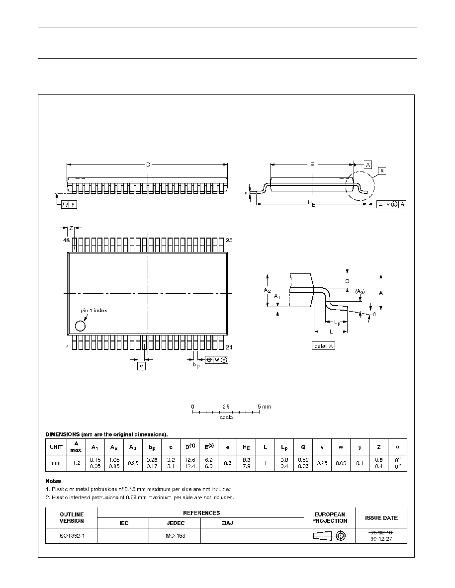
TSSOP48:
plastic thin shrink small outline package; 48 leads; body width 6.1 mm
SOT362-1

Philips Semiconductors
Product data
PCKV857A
100-250 MHz differential 1:10 clock driver
2003 Jul 31
11
TSSOP48:
plastic thin shrink small outline package; 48 leads;
body width 4.4 mm; lead pitch 0.4 mm
SOT480-1

Philips Semiconductors
Product data
PCKV857A
100-250 MHz differential 1:10 clock driver
2003 Jul 31
12
REVISION HISTORY
Rev
Date
Description
_2
20030731
Product data (9397 750 11759); ECN 853-2394 30057 dated 18 June 2003.
Supersedes data of 2002 Decemaber 13 (9397 750 10867).
Modifications:
·
Minor changes or corrections to existing product specifications.
_1
20021213
Product data (9397 750 10867); ECN 853-2394 29181 of 13 December 2002.
Philips Semiconductors
Product data
PCKV857A
100-250 MHz differential 1:10 clock driver
2003 Jul 31
13
Definitions
Short-form specification -- The data in a short-form specification is extracted from a full data sheet with the same type number and title. For detailed information see
the relevant data sheet or data handbook.
Limiting values definition -- Limiting values given are in accordance with the Absolute Maximum Rating System (IEC 60134). Stress above one or more of the limiting
values may cause permanent damage to the device. These are stress ratings only and operation of the device at these or at any other conditions above those given
in the Characteristics sections of the specification is not implied. Exposure to limiting values for extended periods may affect device reliability.
Application information -- Applications that are described herein for any of these products are for illustrative purposes only. Philips Semiconductors make no
representation or warranty that such applications will be suitable for the specified use without further testing or modification.
Disclaimers
Life support -- These products are not designed for use in life support appliances, devices, or systems where malfunction of these products can reasonably be
expected to result in personal injury. Philips Semiconductors customers using or selling these products for use in such applications do so at their own risk and agree
to fully indemnify Philips Semiconductors for any damages resulting from such application.
Right to make changes -- Philips Semiconductors reserves the right to make changes in the products--including circuits, standard cells, and/or software--described
or contained herein in order to improve design and/or performance. When the product is in full production (status `Production'), relevant changes will be communicated
via a Customer Product/Process Change Notification (CPCN). Philips Semiconductors assumes no responsibility or liability for the use of any of these products, conveys
no license or title under any patent, copyright, or mask work right to these products, and makes no representations or warranties that these products are free from patent,
copyright, or mask work right infringement, unless otherwise specified.
Contact information
For additional information please visit
http://www.semiconductors.philips.com.
Fax: +31 40 27 24825
For sales offices addresses send e-mail to:
sales.addresses@www.semiconductors.philips.com.
Koninklijke Philips Electronics N.V. 2002
All rights reserved. Printed in U.S.A.
Date of release: 07-03
Document order number:
9397 750 11759
Philips
Semiconductors
Data sheet status
[1]
Objective data
Preliminary data
Product data
Product
status
[2] [3]
Development
Qualification
Production
Definitions
This data sheet contains data from the objective specification for product development.
Philips Semiconductors reserves the right to change the specification in any manner without notice.
This data sheet contains data from the preliminary specification. Supplementary data will be published
at a later date. Philips Semiconductors reserves the right to change the specification without notice, in
order to improve the design and supply the best possible product.
This data sheet contains data from the product specification. Philips Semiconductors reserves the
right to make changes at any time in order to improve the design, manufacturing and supply. Relevant
changes will be communicated via a Customer Product/Process Change Notification (CPCN).
Data sheet status
[1] Please consult the most recently issued data sheet before initiating or completing a design.
[2] The product status of the device(s) described in this data sheet may have changed since this data sheet was published. The latest information is available on the Internet at URL
http://www.semiconductors.philips.com.
[3] For data sheets describing multiple type numbers, the highest-level product status determines the data sheet status.
Level
I
II
III