Document Outline
- 1 FEATURES
- 2 GENERAL DESCRIPTION
- 3 APPLICATIONS
- 4 ORDERING INFORMATION
- 5 BLOCK DIAGRAM
- 6 PINNING INFORMATION
- 6.1 Pinning
- 6.2 Pinning description
- 7 OVERVIEW OF THE GSM CHIP SET
- 7.1 General
- 7.2 The role of the PCF5083
- 8 FUNCTIONAL DESCRIPTION TIMER CORE
- 8.1 Clock generator
- 8.2 ON/OFF Logic
- 8.2.1 MOBILE SWITCH-ON PROCEDURE
- 8.2.2 MOBILE SWITCH-OFF PROCEDURE
- 8.2.3 OFF TIMER AND WATCHDOG TIMER
- 8.3 Timing Generator
- 8.3.1 THE QUARTERBIT COUNTER
- 8.3.2 NORMAL MODE
- 8.3.3 SLEEP MODE
- 8.4 RF-IC Interface Bus
- 8.4.1 FREQUENCY SETTING CHANNEL
- 8.4.2 GAIN CONTROL CHANNEL
- 8.4.3 IMMEDIATE CONTROL CHANNEL
- 8.4.4 OPERATION MODES AND CONTROL REGISTERS
- 8.5 IOM ® -2 Interface
- 8.5.1 IOM ® -2 CLOCK GENERATION
- 8.5.2 IOM ® -2 MASTER UNIT
- 8.5.3 MONITOR CHANNEL TRANSMITTER PROTOCOL
- 8.5.4 MONITOR CHANNEL RECEIVER PROTOCOL
- 8.5.5 COMMAND/INDICATION CHANNEL TRANSMITTER
- 8.5.6 COMMAND/INDICATION CHANNEL RECEIVER
- 8.5.7 AUDIO INTERFACE
- 8.5.8 EXTERNAL IOM ® -2 INTERFACE
- 8.6 MMI Interface
- 8.6.1 RS232 INTERFACE
- 8.6.2 MMI POWER-DOWN INTERFACE
- 8.7 General purpose parallel I/O port
- 8.8 Real Time Clock
- 8.8.1 SETTING THE REAL TIME CLOCK
- 9 DESCRIPTION OF THE DSP CORE
- 9.1 Interface description
- 9.1.1 BASEBAND DIGITIZER INTERFACE
- 9.1.2 GMSK MODULATOR INTERFACE
- 9.1.3 AUDIO AND DATA I NTERFACE
- 9.1.4 AUDIO INTERFACE
- 9.1.5 TERMINAL ADAPTOR INTERFACE FOR DATA SERVICES
- 9.1.6 SYSTEM CONTROLLER INTERFACE
- 9.1.7 EVENT COUNTER CLOCK
- 9.1.8 GENERAL PURPOSE I/O PINS
- 9.1.9 POWER SAVING MODES
- 9.2 Message Interface to the System Controller
- 9.2.1 EXECUTION OF GSM BASEBAND PROCEDURES
- 9.2.2 NO OPERATION (NOP) COMMAND
- 9.2.3 SOFT RESETTING THE DSP
- 9.2.4 ERROR HANDLING
- 9.3 GSM baseband procedures
- 9.3.1 PROCEDURE DESCRIPTION
- 9.3.2 PERFORMANCE OF GSM BASEBAND PROCEDURES
- 9.4 Software applications
- 9.4.1 RECEIVING A CCH BLOCK
- 9.4.2 TRANSMITTING A CCH BLOCK
- 9.4.3 FB SEARCH FOR TIMING SYNCHRONIZATION
- 9.4.4 PROCESSING A TCH/FS MULTIFRAME
- 10 MICROCONTROLLER INTERFACE
- 10.1 Register Set for the Timer Core
- 10.2 Interrupt Logic
- 11 RESET
- 12 JTAG TEST INTERFACE
- 13 TEST AND EMULATION MODES
- 14 LIMITING VALUES
- 15 DC CHARACTERISTICS
- 17 APPLICATION INFORMATION
- 18 PACKAGE OUTLINE
- 19 SOLDERING

DATA SHEET
Objective specification
File under Integrated Circuits, IC17
1996 Oct 29
INTEGRATED CIRCUITS
PCF5083
GSM signal processing IC

1996 Oct 29
2
Philips Semiconductors
Objective specification
GSM signal processing IC
PCF5083
CONTENTS
1
FEATURES
2
GENERAL DESCRIPTION
3
APPLICATIONS
4
ORDERING INFORMATION
5
BLOCK DIAGRAM
6
PINNING INFORMATION
6.1
Pinning
6.2
Pinning description
7
OVERVIEW OF THE GSM CHIP SET
7.1
General
7.2
The role of the PCF5083
8
FUNCTIONAL DESCRIPTION TIMER CORE
8.1
Clock generator
8.2
ON/OFF Logic
8.2.1
Mobile switch-on procedure
8.2.2
Mobile switch-off procedure
8.2.3
OFF/Watchdog Timer
8.3
Timing Generator
8.3.1
The Quarterbit Counter
8.3.2
Normal Mode
8.3.3
Sleep Mode
8.4
RF-IC Interface Bus
8.4.1
Frequency Setting Channel
8.4.2
Gain Control Channel
8.4.3
Immediate Control Channel
8.4.4
Operation Modes and Control Registers
8.5
IOM
®
-2 Interface
8.5.1
IOM
®
-2 Clock Generation
8.5.2
IOM
®
-2 Master Unit
8.5.3
Monitor Channel Transmitter Protocol
8.5.4
Monitor Channel Receiver Protocol
8.5.5
Command/Indication Channel Transmitter
8.5.6
Command/Indication Channel Receiver
8.5.7
Audio Interface
8.5.8
External IOM
®
-2 Interface
8.6
MMI Interface
8.6.1
RS232 Interface
8.6.2
MMI power-down Interface
8.7
General purpose parallel I/O-port
8.8
Real Time Clock
8.8.1
Setting the real time clock
9
DESCRIPTION OF THE DSP CORE
9.1
Interface description
9.1.1
Baseband Digitizer Interface
9.1.2
GMSK Modulator Interface
9.1.3
Audio and Data Interface
9.1.4
Audio interface
9.1.5
Terminal adaptor interface for data services
9.1.6
System controller interface
9.1.7
Event Counter Clock
9.1.8
Usage of General Purpose I/O Pins
9.1.9
Power saving modes
9.2
Message Interface to the System Controller
9.2.1
Execution of GSM baseband procedures
9.2.2
No Operation (NOP) command
9.2.3
Soft resetting the DSP
9.2.4
Error handling
9.3
GSM baseband procedures
9.3.1
Procedure description
9.3.2
Performance of GSM baseband procedures
9.4
Software applications
9.4.1
Receiving a CCH block
9.4.2
Transmitting a CCH block
9.4.3
FB search for timing synchronization
9.4.4
Processing a TCH/FS multiframe
10
MICROCONTROLLER INTERFACE
10.1
Register Set for the Timer Core
10.2
Interrupt Logic
11
RESET
12
JTAG TEST INTERFACE
13
TEST AND EMULATION MODES
14
LIMITING VALUES
15
DC CHARACTERISTICS
16
AC CHARACTERISTICS
17
APPLICATION INFORMATION
18
PACKAGE OUTLINE
19
SOLDERING
19.1
Introduction
19.2
Reflow soldering
19.3
Wave soldering
19.4
Repairing soldered joints
20
DEFINITIONS
21
LIFE SUPPORT APPLICATIONS

1996 Oct 29
3
Philips Semiconductors
Objective specification
GSM signal processing IC
PCF5083
1
FEATURES
·
Fabricated in a 0.5
µ
m CMOS process with 3-layer
metal
·
LQFP128 package (SOT420AA-2)
·
3.3 V operation
·
Low power
·
Embedded DSP core for all GSM specific signal
processing tasks:
16-bit fixed point DSP
19.5 MHz or external clock operation
Flexible power-down modes
5 kbyte on-chip program or data RAM
2 kbyte on-chip data ROM
16 kbyte on-chip program ROM
Fully pre-programmed modules for GSM baseband
tasks including all data channels
Dedicated GSM signal processor with application
specific hardware for: equalisation, channel
encoding/decoding for all traffic and control channels
and encryption/decryption (A5/1 and A5/2
algorithms)
Tone and side-tone generation
·
GSM Hardware Timer and Interface core:
Power saving Sleep mode for GSM mobiles
Programmable TDMA timing and power-down
signals with 0.25 bit resolution
Three wire serial control bus for fast programming of
RF ICs and synthesizers
IOM
®
-2 interface for external accessories, host
software download and support of the Digital Audio
Interface (DAI)
RS232 interface for the man machine interface
controller
Man machine interface power-down control
Power supply control logic with Watchdog Timer
Real time clock and calendar running on 32.768 kHz
6-bit general purpose I/O port
·
Reduced swing 13 MHz main clock input
·
On-chip PLL to derive the DSP and microcontroller clock
·
8-bit, 68000 compatible host interface with three
interrupt lines
·
Boundary scan interface in accordance with
"IEEE Standard 1149.1-1990".
2
GENERAL DESCRIPTION
The PCF5083 GSM Signal Processing IC is a dedicated
VLSI circuit; fabricated in a 0.5
µ
m CMOS process. It has
been designed for baseband signal processing tasks for
the Pan European Global System for Mobile
telecommunication (GSM). The PCF5083 is part of the
second generation Philips Semiconductors GSM chip set.
The PCF5083 consists of an embedded 16-bit DSP core
for all GSM specific signal processing tasks and a Timer
and Interface core which contains many peripheral
functions to simplify the system design.
3
APPLICATIONS
The PCF5083 is suitable for use in GSM mobile stations or
hand-helds.
4
ORDERING INFORMATION
TYPE NUMBER
PACKAGE
NAME
DESCRIPTION
VERSION
PCF5083H/F2
LQFP128
plastic low profile quad flat package; 128 leads; (PCF5083-2B)
SOT420-1
PCF5083H/001/F2
LQFP128
plastic low profile quad flat package; 128 leads; (PCF5083-2C)
SOT420-1
PCF5083H/5V2/F3
LQFP128
plastic low profile quad flat package; 128 leads; (PCF5083-3A)
SOT420-1

1996 Oct 29
4
Philips Semiconductors
Objective specification
GSM signal processing IC
PCF5083
5
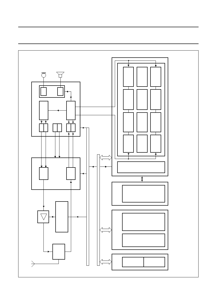
BLOCK DIAGRAM
Fig.1 Block diagram.
handbook, full pagewidth
SERIAL
X-PORT
AND
Y-PORT
I/O-PORT
HOST PORT
EMBEDDED
DSP-CORE
IOM-2
INTERFACE
AND
AUDIO INTERFACE
HOST
INTERFACE
INTERRUPT
LOGIC
CLOCK
GENERATOR
AND
PLL
ON / OFF
LOGIC
JTAG
AND
TEST
REAL TIME
CLOCK
RF-IC
INTERFACE
MMI
INTERFACE
PARALLEL
PORT
TIMING
GENERATOR
SIXCLK
SIXEN
SIXD
SOXCLK
SOXEN
SOXD
FSC
DCL
DU
DD
AFS
ACLK
ADI
ADO
RXON
TXON
BEN
PDRX1
PDRX2
PDTX1
NPDTX1
NPDTX2
PDBIAS
NPDBIAS
PDSYN
TXKEY1
TXKEY2
GPON1
GPON2
REFON
NREFON
RFCLK
RFEN1
RFEN2
RFEN3
RFEN4
RFDI
RFDO
RFE
RXD
TXD
MMICLK
MMIIREQ
PIO1 to PIO5
MGE284
IO1/AEN
IO2
IO3/IRQN2
IO4/DTX
HD0 to HD7
HA0 to HA6
HR/W
CKI
CKO
CLK13M
CLK20M
DCLK
CLKSEL
CLK32I
CLK32O
CLK32K
ONKEY
AUXON
POWON
NPOWON
TCK
TMS
TDI
TDO
TRSTN
TCKIO
TCE
TSCK1
TSCK2
DSPEN
TIMEN
HCEN_T
FRAME_INT
HCEN_D
DTACK
COMB_INT
HIPR_INT
LOWVOLT
RSTP
RST
MMIEN
RSTC
RSTO
1996 Oct 29
5
Philips Semiconductors
Objective specification
GSM signal processing IC
PCF5083
6
PINNING INFORMATION
6.1
Pinning
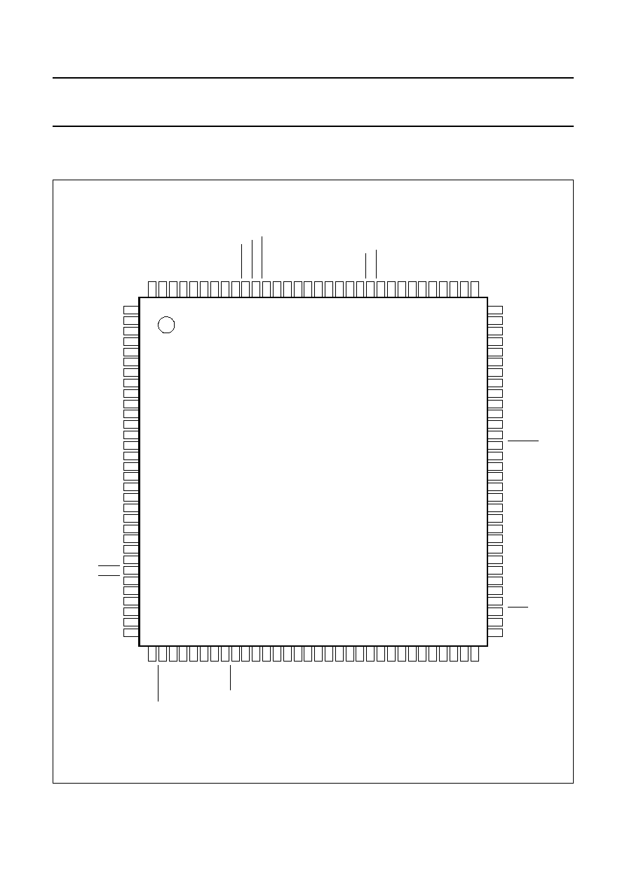
Fig.2 Pin configuration - PCF5083-2B and PCF5083-2C.
MGE282
PCF5083
1
2
3
4
5
6
7
8
9
10
11
12
13
14
15
16
17
18
19
20
21
22
23
24
25
26
27
28
29
30
31
32
80
79
78
77
76
75
74
73
72
71
70
69
68
67
66
65
96
95
94
93
92
91
90
89
88
87
86
85
84
83
82
81
VDD2
VDDPLL
VDD1
VSS1
VSSPLL
VSS2
VSS2
VDD1
VSS1
VSS1
VDD1
VDD2
128
127
126
125
124
123
122
121
120
119
118
117
116
115
114
113
112
111
110
109
108
107
106
105
104
103
102
101
100
99
98
97
33
34
35
36
37
38
39
40
41
42
43
44
45
46
47
48
49
50
51
52
53
54
55
56
57
58
59
60
61
62
63
64
handbook, full pagewidth
RXON
TXON
BEN
PDRX1
PDRX2
PDTX1
NPDTX1
NPDTX2
PDBIAS
NPDBIAS
PDSYN
TXKEY1
TXKEY2
REFON
PIO1
PIO2
PIO3
PIO4
PIO5
IO1/AEN
IO2
IO3/IRQN2
IO4/DTX
HD0
HD1
HA6
HA5
HA4
HA3
HA2
HA1
HA0
HCEN_T
CKI
CKO
DCLK
CLKSEL
RSTP
CLK32I
CLK32O
ONKEY
V
SS2
V
DD1
V
SS1
V
DD2
V
DD2
V
SSPLL
FSC
DCL
DU
DD
GPON1
GPON2
NREFON
RFCLK
RFEN1
RFEN2
RFEN3
RFEN4
RFDI
RFDO
RFE
RXD
TXD
MMIEN
MMICLK
MMIIREQ
CLK32K
AUXON
LOWVOLT
POWON
NPOWON
RST
RSTO
RSTC
TCK
TMS
TDI
TDO
TRSTN
TCKIO
TCE
V
DD1
V
SS1
V
SS2
V
DD2
V
DD1
V
SS1
SIXCLK
SIXEN
SIXD
SOXCLK
SOXEN
SOXD
AFS
ACLK
ADI
ADO
HD2
HD3
HD4
HD5
HD6
HD7
HR/W
HCEN_D
DTACK
FRAME_INT
COMB_INT
HIPR_INT
CLK13M
CLK20M
TSCK1
TSCK2
DSPEN
TIMEN
1996 Oct 29
6
Philips Semiconductors
Objective specification
GSM signal processing IC
PCF5083
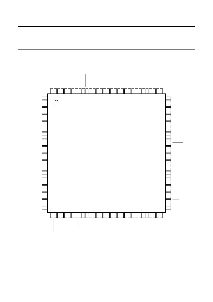
Fig.3 Pin configuration - PCF5083-3A.
MGD706
PCF5083
1
2
3
4
5
6
7
8
9
10
11
12
13
14
15
16
17
18
19
20
21
22
23
24
25
26
27
28
29
30
31
32
80
79
78
77
76
75
74
73
72
71
70
69
68
67
66
65
96
95
94
93
92
91
90
89
88
87
86
85
84
83
82
81
VDD2
VDDPLL
VDD1
VSS1
VSSPLL
VSS2
VSS2
VDD1
VSS1
VSS1
VDD1
VDD2
128
127
126
125
124
123
122
121
120
119
118
117
116
115
114
113
112
111
110
109
108
107
106
105
104
103
102
101
100
99
98
97
33
34
35
36
37
38
39
40
41
42
43
44
45
46
47
48
49
50
51
52
53
54
55
56
57
58
59
60
61
62
63
64
handbook, full pagewidth
RXON
TXON
BEN
PDRX1
PDRX2
PDTX1
NPDTX1
NPDTX2
PDBIAS
NPDBIAS
PDSYN
TXKEY1
TXKEY2
REFON
PIO1
PIO2
PIO3
PIO4
PIO5
IO1/AEN
IO2
IO3/IRQN2
IO4/DTX
HD0
HD1
HA6
HA5
HA4
HA3
HA2
HA1
HA0
HCEN_T
CKI
CKO
DCLK
CLKSEL
RSTP
CLK32I
CLK32O
ONKEY
V
SS2
V
DD1
V
SS1
V
DD2
V
DD2
V
SSPLL
FSC
DCL
DU
DD
GPON1
GPON2
NREFON
RFCLK
RFEN1
RFEN2
RFEN3
RFEN4
RFDI
RFDO
RFE
RXD
TXD
MMIEN
MMICLK
MMIIREQ
CLK26M
AUXON
LOWVOLT
POWON
NPOWON
RST
RSTO
RSTC
TCK
TMS
TDI
TDO
TRSTN
TCKIO
TCE
V
DD1
V
SS1
V
SS2
V
DD2
V
DD1
V
SS1
SIXCLK
SIXEN
SIXD
SOXCLK
SOXEN
SOXD
AFS
ACLK
ADI
ADO
HD2
HD3
HD4
HD5
HD6
HD7
HR/W
HCEN_D
DTACK
FRAME_INT
COMB_INT
HIPR_INT
CLK13M
CLK20M
TSCK1
TSCK2
DSPEN
TIMEN

1996 Oct 29
7
Philips Semiconductors
Objective specification
GSM signal processing IC
PCF5083
6.2
Pinning description
SYMBOL
PIN
I/O
DESCRIPTION
TCE
1
I
Test Clock Enable (active HIGH); tied to V
SS
during normal operation.
PIO1 to PIO5
2 to 6
I/O
General purpose parallel port (3-state output).
BEN
7
O
Baseband Port Enable (active HIGH, 3-state).
TXON
8
O
Modulator window enable (active HIGH, 3-state).
RXON
9
O
Receiver window enable (active HIGH, 3-state).
V
SS1
10
Ground I/O pin.
V
DD1
11
Supply I/O pin.
PDRX1
12
O
Receiver Power-down 1 (active HIGH, 3-state).
PDRX2
13
O
Receiver Power-down 2 (active HIGH, 3-state).
PDTX1
14
O
Transmitter Power-down 1 (active HIGH, 3-state).
NPDTX1
15
O
Inverted output of PDTX1 (active LOW, 3-state).
V
DD2
16
Supply core.
V
SS2
17
Ground core.
NPDTX2
18
O
Transmitter Power-down 2 (active LOW, 3-state).
PDBIAS
19
O
Transmitter power supply Power-down (active HIGH, 3-state).
NPDBIAS
20
O
Inverted output of PDBIAS (active LOW, 3-state).
PDSYN
21
O
Synthesizer Power-down (active HIGH, 3-state).
TXKEY1
22
O
Power ramping control (active HIGH, 3-state).
TXKEY2
23
O
Power module control (active HIGH, 3-state).
DSPEN
24
I
DSP Test Mode Enable (active HIGH). PCF5083-2B includes an internal
pull-down resistor. PCF5083-2C does not include an internal pull-down resistor.
TIMEN
25
I
Timer Test Mode Enable (active HIGH). PCF5083-2B includes an internal
pull-down resistor. PCF5083-2C does not include an internal pull-down resistor.
RSTC
26
I
Asynchronous Reset - real time clock (active LOW, CMOS level Schmitt trigger
input).
RSTO
27
I
Asynchronous Reset - ON/OFF logic (active LOW, CMOS level Schmitt trigger
input).
V
DD1
28
Supply I/O pin.
CLK32O
29
O
32.768 kHz crystal oscillator output.
CLK32I
30
I
32.768 kHz crystal oscillator input.
V
SS1
31
Ground I/O pin.
ONKEY
32
I
ON/OFF Key input (active HIGH, CMOS level Schmitt trigger input with internal
pull-down resistor).

1996 Oct 29
8
Philips Semiconductors
Objective specification
GSM signal processing IC
PCF5083
AUXON
33
I
Auxiliary Switch on input (active HIGH, CMOS level Schmitt trigger input).
LOWVOLT
34
I
Low battery indication (active LOW, CMOS level Schmitt trigger input).
POWON
35
O
Power Regulator on (active HIGH).
NPOWON
36
O
Power Regulator on (active LOW).
RST
37
I
Asynchronous Reset for timer section (active LOW, CMOS level Schmitt trigger
input).
CLK32K
38
O
The 32.768 kHz CMOS level output for PCF5083-2B and PCF5083-2C.
CLK26M
The 26 MHz CMOS level output for PCF5083-3.
TXD
39
O
RS232 transmit data output (open-drain output).
RXD
40
I
RS232 receive data input.
MMIEN
41
O
RS232 input buffer full indication (active LOW, open-drain output).
MMIREQ
42
I
MMI clock request (active HIGH, CMOS level Schmitt trigger input).
MMICLK
43
O
MMI clock 13 MHz.
FSC
44
I/O
IOM
®
-2 frame pulse (3-state).
DCL
45
I/O
IOM
®
-2 clock (3-state).
DU
46
I
IOM
®
-2 data input (CMOS level Schmitt trigger input).
DD
47
O
IOM
®
-2 data output (open drain output).
V
SS2
48
Ground core.
V
DD1
49
Supply I/O pin.
V
SS1
50
Ground I/O pin.
V
DD2
51
Supply core.
RFCLK
52
O
RF
-
IC interface shift clock (3-state).
RFEN1
53
O
RF
-
IC Interface Enable 1(active LOW, 3-state).
RFEN2
54
O
RF
-
IC Interface Enable 2 (active LOW, 3-state).
RFEN3
55
O
RF
-
IC Interface Enable 3 (active LOW, 3-state).
RFEN4
56
O
RF
-
IC Interface Enable 4 (active LOW, 3-state).
V
DD2
57
Supply core.
V
SSPLL
58
Ground for PLL.
RFDI
59
I
RF
-
IC Interface data in.
RFDO
60
O
RF
-
IC Interface data out (3-state).
RFE
61
O
RF
-
IC Interface Enable (active HIGH, 3-state).
NREFON
62
O
Reference oscillator power-down (active LOW, 3-state).
SYMBOL
PIN
I/O
DESCRIPTION

1996 Oct 29
9
Philips Semiconductors
Objective specification
GSM signal processing IC
PCF5083
GPON1
63
O
Sleep mode power-down 1 (active HIGH, 3-state).
GPON2
64
O
Sleep mode power-down 2 (active HIGH, open-drain output).
REFON
65
O
Sleep mode power-down 3 (active HIGH, 3-state).
DCLK
66
I
External DSP clock input.
RSTP
67
I
PLL reset (active LOW with internal pull-down resistor).
CLKSEL
68
I
Timer clock source select.
V
SSPLL
69
Ground for PLL.
CKO
70
O
Low swing input buffer output.
V
SS1
71
Ground I/O pin.
V
DD1
72
Supply I/O pin.
CKI
73
I
Reference clock input, low swing input 13 kHz.
V
DDPLL
74
Supply for PLL.
TMS
75
I
JTAG port mode select (with internal pull-down resistor).
TDI
76
I
JTAG port data input (with internal pull-down resistor).
TDO
77
O
JTAG port data output.
TCKIO
78
I
Auxiliary test signal - tied to V
SS
during operation.
TRSTN
79
I
JTAG port reset (with internal pull-down resistor).
V
DD2
80
Supply core.
V
SS2
81
Ground core.
TCK
82
I
JTAG port clock input (with internal pull-down resistor).
HCEN_T
83
I
Host Interface Enable - Timer core (active LOW).
IO1/AEN
84
I/O
DSP general purpose I/O used for voice port control (CMOS level I/O). The
PCF5083-3 has its own internal pull-up resistor however, both the PCF5083-2B
and PCF5083-2C require a pull-up resistor.
IO2
85
I/O
DSP general purpose I/O used for voice port control (CMOS level I/O). The
PCF5083-3 has its own internal pull-up resistor however, both the PCF5083-2B
and PCF5083-2C require a pull-up resistor.
IO3/IRQN2
86
I/O
DSP general purpose I/O or Interrupt Request Input 2 (CMOS level I/O). The
PCF5083-3 has its own internal pull-up resistor however, both the PCF5083-2B
and PCF5083-2C require a pull-up resistor.
IO4/DTX
87
I/O
DSP general purpose I/O (CMOS level I/O, external pull-up resistor required).
HA0 to HA6
88 to 94
I
Host Interface Address.
HD0 to HD3
95 to 98
I/O
Host Interface Data (3-state).
SYMBOL
PIN
I/O
DESCRIPTION

1996 Oct 29
10
Philips Semiconductors
Objective specification
GSM signal processing IC
PCF5083
V
SS1
99
Ground I/O pin.
V
DD1
100
Supply I/O pin.
HD4 to HD7
101 to 104 I/O
Host Interface data (3-state).
HR/W
105
I
Host Interface Write Enable.
HCEN_D
106
I
Host Interface Enable - DSP core (active LOW).
DTACK
107
O
Host port acknowledge - used as DTACK from DSP core (active LOW, open-drain
output).
SIXCLK
108
I
DSP serial input port X clock (CMOS level Schmitt trigger input).
SIXEN
109
I
DSP serial input port X enable.
SIXD
110
I
DSP serial input port X data.
SOXCLK
111
I
DSP serial output port X clock (CMOS level Schmitt trigger input).
V
DD2
112
Supply core.
V
SS2
113
Ground core.
SOXEN
114
I
DSP serial output port X enable.
SOXD
115
O
DSP serial output port X data (3-state).
CLK20M
116
O
19.5 MHz CMOS level output.
FRAME_INT
117
O
TDMA frame interrupt (active LOW, open drain output).
COMB_INT
118
O
Combined interrupt (active LOW, open drain output).
HIPR_INT
119
O
High Priority Interrupt (active LOW, open drain output).
CLK13M
120
O
13 MHz CMOS level output.
V
SS1
121
Ground I/O pin.
V
DD1
122
Supply I/O pin.
AFS
123
I/O
Audio Interface frame sync signal (3-state).
ACLK
124
I/O
Audio Interface Clock (3-state).
ADI
125
I
Audio Interface Data In, RS232 clock if enabled.
ADO
126
O
Audio Interface Data Out (3-state).
TSCK1
127
I
Test Clock 1 - tied to V
SS
during normal operation.
TSCK2
128
I
Test Clock 2 - tied to V
DD2
during normal operation.
SYMBOL
PIN
I/O
DESCRIPTION

1996 Oct 29
11
Philips Semiconductors
Objective specification
GSM signal processing IC
PCF5083
7
OVERVIEW OF THE GSM CHIP SET
7.1
General
The chip set's high-level architectural modularity ensures
that it can be easily adapted to meet various market
requirements in terms of hardware and software. Figure 4
is a simplified block diagram of a GSM terminal using the
Philips Semiconductors chip set.
The receiver converts the antenna input signal from
890 to 915 MHz down into a complex baseband signal
consisting of an in-phase (I) and a quadrature
component (Q). In order to deal with the high dynamic
range from
-
104 to
-
10 dBm, the receiver provides an
AGC input controlled by the layer 1 software in the System
Controller. The complex baseband signal is connected to
the input of the PCF5072 baseband interface IC. This IC
samples the I and Q components at the GSM bit clock
(270 kHz) with an accuracy of approximately 2
×
13 bits.
The equalizer is responsible for the following tasks:
·
Channel impulse response estimation and bit
synchronization by means of the training sequence
·
Adaptive channel equalization with a modified Maximum
Likelihood Sequence Estimation (MLSE) approach that
produces a bit-by-bit soft decision information (Channel
Measurement Information (CMI)
·
Channel impulse response adaption and frequency
offset estimation.
After decryption the channel decoder performs
convolutional and block decoding. Depending on the
logical channel in use, there are decoding schemes for
TCH/F (FACCH/F), SACCH and SDCCH.
The speech decoder synthesises the audio signal from the
received bit stream. Updating of comfort noise parameters
occurs each time a valid Silence Descriptor (SID) is
received. Comfort noise is inserted during periods of
speech pauses. Substitution and muting of lost or bad
frames is implemented.
The full rate speech encoder collects speech samples of
13-bit uniform PCM format (104 kbits/s) and compresses
them to 13 kbits/s according to the linear predictive coding,
long term prediction, Regular Pulse Excitation (RPE-LTP).
Discontinuous Transmission (DTX) is available (voice
activity detection, background acoustic noise).
To protect the data from transmission errors, block and
convolutional coders form the channel encoder. The
encoding modules relates to the logical channels (e.g.
RACH, TCH/F (FACCH/F), SDCCH/SACCH).
After encryption the burst builder generates either Normal
Bursts (NB) or Access Bursts (AB). The bit-stream is then
modulated with a GMSK modulator (Gaussian Minimum
Shift Keying) and upconverted in a quadrature mixer to
890 to 915 MHz.
The on-chip GSM timer generates all power-down and
control signals for the receiver, the transmitter, the
P90CL301 System Controller and the PCF5072 baseband
interface IC.
The System Controller (P90CL301) services all HW
interfaces and performs the signalling software contained
in the GSM layer stack (with L1, L2, L3, O&M, UAP,
SIMAP etc).
The voiceband ADCs and DACs of the PCF5072 perform
the conversion between the analog audio signals and the
digital domain.
7.2
The role of the PCF5083
The PCF5083 is a dedicated VLSI circuit offering
baseband signal processing tasks for the Pan European
Global System for Mobile telecommunication (GSM). The
PCF5083 can be applied in GSM mobile stations or
hand-helds. The embedded DSP core is optimized for
GSM baseband functions and contains an on-chip
program ROM featuring the following tasks:
·
Full rate speech coding/decoding including VAD/DTX
(
"GSM 06 series" )
·
Encryption/decryption according to both A5/1 and A5/2
algorithms (
"GSM Rec. 3.20, 3.21" )
·
Burst building supporting access burst and normal burst
(
"GSM Rec. 5.02")
·
Frequency Correction Burst (FCB) detection and
evaluation
·
Synchronization burst (SCH) detection
·
BCCH monitoring of neighbouring cells
·
Channel coding/decoding and
interleaving/de-interleaving (
"GSM Rec. 5.03") for:
Broadcast Channels (BCH): SCH, BCCH
Common Control Channels (CCCH): PCH, RACH,
AGCH
Dedicated Control Channels (DCH): SDCCH,
SACCH
Traffic Channels (TCH): TCH/FS, TCH/F2.4,
TCH/F4.8, TCH/F9.6, TCH/H4.8 and TCH/H2.4
Associated Control Channels (ACCH): FACCH and
SACCH

1996 Oct 29
12
Philips Semiconductors
Objective specification
GSM signal processing IC
PCF5083
·
Equalization for normal and synchronization bursts
·
Power measurement of serving and neighbouring cells
·
Tone and side-tone generation.
2.5 kbytes of RAM are free for downloading of additional
software modules e.g. rate adaptation, handsfree, voice
recognition.
The DSP communicates via two serial ports to the
baseband interface IC and to the IOM
®
-2 Interface and
Voice Port for speech and data transmission. For
command and data transfer it is connected to a
microcontroller via its 8-bit Host Port and the
68000 compatible Host Interface. The I/O port of the DSP
core provides four general purpose I/O lines. Some of the
port lines are used as dedicated control signals.
The Timer and Interface functions include a GSM specific
hardware timer and a couple of interface functions which
simplify system design and keep the chip count to a
minimum.
The Timing Generator provides the TDMA burst timing and
power on/off signals for the RF transmitter, RF receiver,
synthesizer, DSP and baseband interface IC. The timing
signals can be programmed with an accuracy of a
quarterbit (
1
/
500
TDMA frame). Their output polarity is
programmable.
The RF-IC Interface is used to program the RF ICs and the
synthesizer. It is compatible with the Philips `Three Wire
Bus' and other standards. The bus consists of clock, data
and several enable lines to transfer data between the
PCF5083 and the connected devices. ICs of one family
share the same enable line. Their unique address is a part
of the data stream. ICs of different families use separate
enable lines.
The PCF5083 includes an IOM
®
-2 Interface to connect
external accessories e.g. a handsfree set. It may be used
as a software download interface and provides access for
the Digital Audio Interface during Type Approval.
The Audio Interface provides the connection between a
local codec, the IOM
®
-2 Bus and the DSP.
The ON/OFF Logic performs the basic power-up and
power-down switching function for the whole mobile. It
controls the supply voltage switches for the terminal. The
on/off conditions are controlled via the operators
keyboard, a low voltage battery indication circuit, the
Watchdog Timer or an auxiliary switch on input for general
purpose use.
The man-machine interface section includes a dedicated
RS232 interface and generates a 13 MHz clock for the
keyboard and card reader controller. If this controller is
inactive, the clock is stopped to save power. If the
controller requests service, the clock is switched on again.
The PCF5083 includes a 6-bit general purpose parallel
port to control system functions. One bit of the port is used
on-chip to provide a reset signal for the DSP core.
The PCF5083 is accessed via its 8-bit, 68000 compatible
Host Interface. Separate chip enable lines for the DSP and
the Timer core are available. The DSP core provides a
signal to be used as DTACK for maximum speed
operation. Three interrupt lines are provided for the
microcontroller.
The PCF5083 requires two clock signals. The 13 MHz
main clock is used internally to generate the TDMA timing
and as a reference clock for the on-chip PLL. A second
clock of 32.768 kHz is used for a real time clock/calendar,
a Watchdog Timer and to provide timing in a power
reducing Sleep mode. During this mode TDMA timing is
maintained with slow running, high accuracy counters,
while all timing signals are kept inactive to save power.
The on-chip PLL generates three clocks (13, 39 and
52 MHz) which are manipulated to generate the internal
DSP clock (19.5 MHz), a 19.5 MHz output (CLK20M) and
a 26 MHz output (CLK26M, only version 3) used by the
microcontroller and other system components. The
13 MHz PLL output is used by the Timing Generator in
addition to being fed back to the PLL. The nominal duty
cycle of the PLL outputs is 50%, independent of the
reference clock characteristics. The PLL clock outputs
may be used for all system components requiring a
symmetric input clock therefore leading to reduced
tolerance requirements for the duty cycle of the reference
clock.
Other ICs of the Philips second generation GSM chipset
are:
·
P90CL301: 16-bit 68000 compatible microcontroller
·
TDA8005: SIM/MMI-Controller
·
PCF5072: Baseband Interface and Audio Codec
·
SA1638: IF processing IC
·
SA1620: RF processing IC (900 MHz)
·
UMA1019: Synthesizer
·
PCF5075: Power amplifier controller
·
BGY20x: UHF Power Amplifier Module family.
1996 Oct 29
13
Philips Semiconductors
Objective specification
GSM signal processing IC
PCF5083
dbook, full pagewidth
MGE283
SPEECH
DECODER
SPEECH
ENCODER
TONE AND
SIDE TONE
GENERATION
CHANNEL
DECODER
CHANNEL
ENCODER
SYSTEM
CONTROLLER
INTERFACE
PCF5075
POWER AMPLIFIER
CONTROLLER
DUPLEX
FILTER
BGY20x
DECRYPTION
A5/1
+
A5/2
ENCRYPTION
A5/1
+
A5/2
MONITORING
EQUALISER
8-bit parallel port
audio
interface
(IOM-2)
BURST
BUILDING
SYNCHRO-
NISATION
TIMER
CORE
SIM,
DISPLAY,
KEYBOARD
PERIPHERY
SYSTEM
CPU
RAM
system control bus
transceiver control bus
ROM
DSP CORE
TDA8005
P90CL301
MEMORY
PCF5083
PCF5072
SA1620 and SA1638
DSP
INTERFACE
RX
TRANSCEIVER
TX
GMSK
MODULATOR
ADC
BBI
ADC
DAC
DAC
DAC
DAC
ADC
DAC
AFC
I
Q
I
Q
AGC
PCM
codec
Fig.4 Simplified block diagram of a GSM terminal with the PCF5083.

1996 Oct 29
14
Philips Semiconductors
Objective specification
GSM signal processing IC
PCF5083
8
FUNCTIONAL DESCRIPTION TIMER CORE
8.1
Clock generator
The Clock Generator consists of a low swing input buffer
for the 13 MHz reference clock, a PLL as frequency
multiplier and a 32.768 kHz crystal oscillator. The PLL
generates 13 MHz, 39 MHz and 52 MHz from the 13 MHz
reference clock. The PLL reset input RSTP is used to bring
the PLL into a low-power state when set to a LOW level.
The 13 MHz reference clock is AC coupled to input CKI.
CKI is a reduced swing input which requires a signal in the
range of 0.7 V
(p-p)
(worst case) for operation. The clock
signal is amplified and used as the input clock for the PLL.
The Timer core is either clocked with the 13 MHz
reference clock or the 13 MHz PLL output. The clock
source is selected with input CLKSEL as shown in Table 1.
Table 1
Timer Core clock selection
CLKSEL
TIMER CORE CLOCK
0
PLL output
1
buffered CKI input
Using the PLL output reduces the tolerance requirements
for the duty cycle of the reference clock.
The DSP core will function with the 39 MHz PLL clock or
the clock supplied from DCLK. The clock source is
selected with the flags in SYSCON_REG; see Tables 2
and 3. Within the DSP core the selected clock is first
halved before use. The 52 MHz PLL is register selectable
for future applications but should not be used in the current
implementation of this device
The inverting buffer stage between CLK32I and CLK32O,
together with an external crystal network generates a
32.768 kHz clock for the Timer Core. This clock is used for
the real time clock, the ON/OFF logic etc.
The internal 13 MHz, 19.5 MHz and 2b/2c: 32.768 kHz/
3: 26 MHz clocks are externally available for other system
components, e.g. the microcontroller. All clock outputs can
be disabled if they are not used to reduce the power
consumption.
Table 2
System Configuration Register (SYSCON); note 1
Note
1. Default value after reset 0X00 0000b (x: LOCK is undefined).
2. Versions PCF5083-2b and PCF5083-2c only.
3. PCF5083-3 only.
BIT
FLAG
R/W
DESCRIPTION
7
-
-
Reserved
6
LOCK
R
PLL lock select. If LOCK = 0; then PLL in lock. If LOCK = 1; then PLL out of
lock.
5
RS232_CLK
W
RS232 interface clock source. If RS232_CLK = 0; then the 13 MHz Timer
clock is used. If RS232_CLK = 1; then the RS232 clock is supplied via the ADI
pin (pin 125).
4
DSP_CLK1
W
DSP clock select. This two bits select the DSP clock frequency; see Table 3.
3
DSP_CLK0
W
2
CLK32K
(2)
W
CLK32K output enable/disable. If CLK32K = 0; then the CLK32K output is
enabled. If CLK32K = 1; then the CLK32K output is disabled.
CLK26M
(3)
CLK26M output enable/disable. If CLK26M = 0; then the CLK26M output is
enabled. If CLK26M = 1; then the CLK26M output is disabled.
1
CLK20M
W
CLK20M output enable/disable. If CLK20M = 0; then the CLK20M output is
enabled. If CLK20M = 1; then the CLK20M output is disabled.
0
CLK13M
W
CLK13M output enable/disable. If CLK13M = 0; then the CLK13M output is
enabled. If CLK13M = 1; then the CLK13M output is disabled.
1996 Oct 29
15
Philips Semiconductors
Objective specification
GSM signal processing IC
PCF5083
Table 3
Selection of the DSP clock
DSP_CLK1
DSP_CLK0
DSP CLOCK
0
0
DCLK/2
0
1
26 MHz
1
0
19.5 MHz
1
1
Reserved
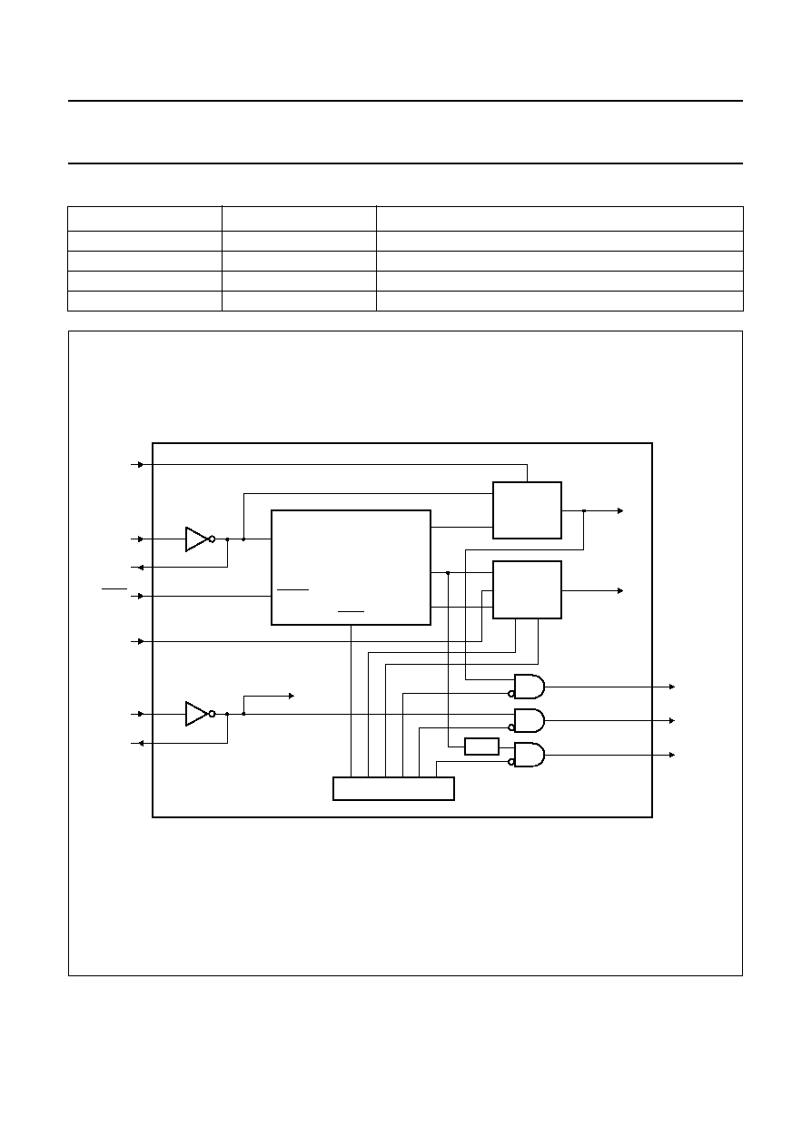
Fig.5 Clock generator block diagram.
handbook, full pagewidth
MGE287
PLL
MUX
13 MHz
13 MHz
CKO
CKI
DCLK
CLKSEL
CLK32I
CLK13M
CLK32K
CLK20M
CLK32O
SEL
clock
timer core
clock
DSP core
MUX
SEL
SYSCON_REG
RESET
RSTP
LOCK
39 MHz
52 MHz
CRYSTAL
OSCILLATOR
LOW SWING
INPUT BUFFER
÷
2
32.768 kHz clock
DSP and timer core

1996 Oct 29
16
Philips Semiconductors
Objective specification
GSM signal processing IC
PCF5083
Fig.6 Clock generator block diagram.
handbook, full pagewidth
MGD705
PLL
MUX
13 MHz
13 MHz
CKO
CKI
DCLK
CLKSEL
CLK32I
CLK13M
CLK26M
CLK20M
CLK32O
SEL
clock
timer core
clock
DSP core
MUX
SEL
SYSCON_REG
RESET
RSTP
LOCK
39 MHz
52 MHz
CRYSTAL
OSCILLATOR
LOW SWING
INPUT BUFFER
÷
2
32.768 kHz clock
DSP and timer core
÷
2

1996 Oct 29
17
Philips Semiconductors
Objective specification
GSM signal processing IC
PCF5083
8.2
ON/OFF Logic
The ON/OFF logic performs the main power on and off
switching function for the whole mobile. The on/off
conditions are controlled via an operators keyboard, a low
voltage battery indication circuit, a hardware Watchdog
Timer or an auxiliary switch on input for general purpose
use.
The hardware control interrupt HWCTRL_INT, signalled
via the COMB_INT output (refer to Section 10.2), is used
to signal the status of the ON/OFF Logic. The inputs
DSPEN and TIMEN are used to control the Watchdog
function. RST and RSTO are asynchronous reset lines.
The inputs ONKEY, AUXON and LOWVOLT are
debounced with a time constant of 62.5 ms. The minimum
pulse width for the safe detection of a signal transition is
therefore 2
×
62.5 = 125 ms on any of these lines. The
ON/OFF Logic signals are specified in Table 4.
Table 4
ON/OFF Logic signals
SIGNAL
DESCRIPTION
ONKEY
Input (active HIGH) to be connected to the
ON/OFF switch of the operators keyboard.
AUXON
Input (edge sensitive) for general purpose
use, e.g. used as battery charger connect
indication or ignition sense in mobile
applications.
LOWVOLT
Input (active LOW) to be connected to an
external low battery indication circuit.
POWON
Output (active HIGH) to be connected to
the ON terminal of the supply voltage
switch.
NPOWON
Inverted output signal of POWON.
8.2.1
M
OBILE SWITCH-ON PROCEDURE
Switching on the mobile is initiated via the PCF5083
according to Table 5.
If one of the three conditions ONKEY, AUXON or Alarm
time match become true, a corresponding flag is set in
register HWCTRL_REG. As soon as one of these flags is
set, signal POWON is set and NPOWON is reset. At the
same time the HWCTRL_INT interrupt is activated. The
interrupt condition is signalled via the COMB_INT line to
the System Controller if the relevant bit is set in the
COMBINT_REG register (refer to Section 10.2).
The hardware reset RST clears the enable bits for the
COMB_INT interrupt lines.
The interrupt flags in register HWCTRL_REG must be
cleared by the System Controller to deactivate the
interrupt condition. A flag is cleared by writing a logic 1 to
its bit location.
The POWON output is the main power control signal. As
soon as POWON goes HIGH, all ICs in the mobile are
powered via the supply voltage switch. The LOWVOLT
input asserted LOW, indicating a low voltage situation, or
RSTO asserted LOW inhibits the mobile to be switched on.
If the PCF5083 was switched on via AUXON
(HWCTRL_REG[AUXON_LH] = 1) and the AUXON signal
remains HIGH, the flag HWCTRL_REG[AUXON_LH] must
be cleared, before the PCF5083 enters the Power-down
mode.
Table 5
Mobile switch-on conditions
RST0
LOWVOLT
ONKEY
AUXON
ALARM TIME MATCHES
CURRENT TIME
POWON
COMB_INT
L
X
X
X
X
L
3-state
H
L
X
X
X
L
3-state
H
H
L
ˇ
H
X
X
L
ˇ
H
H
ˇ
L
H
H
X
L
ˇ
H
X
L
ˇ
H
H
ˇ
L
H
H
X
X
yes
L
ˇ
H
H
ˇ
L

1996 Oct 29
18
Philips Semiconductors
Objective specification
GSM signal processing IC
PCF5083
8.2.2
M
OBILE SWITCH-OFF PROCEDURE
The switch-off request to the System Controller is initiated
via a LOW-to-HIGH transition and hold of pin ONKEY for
longer than 1 second or a LOW level on pin LOWVOLT.
The HWCTRL_INT interrupt is activated if one of these
conditions has set it's corresponding flag in register
HWCTRL_REG.
The next step is to deactivate the POWON signal.
Therefore the flag HWCTRL_REG[SWOFF] has to be set.
If the SWOFF flag is not set within 8 seconds (see
Section 8.2.3) and the Watchdog Timer expires, POWON
is deactivated without any further interaction. The SWOFF
flag is automatically cleared when the mobile is switched
on again.
The PCF5083 is immediately and under all conditions
forced into the off state with RSTO asserted LOW.
Table 6
Mobile switch-off request conditions
ONKEY
LOWVOLT
COMB_INT
H
H
H
L
ˇ
H
X
H
ˇ
L
X
H
ˇ
L
H
ˇ
L
It should be noted that:
·
If POWON is LOW (switch-off state), all outputs of the
PCF5083 except POWON and NPOWON are in their
high-impedance state.
·
The hardware control interrupt (HWCTRL_INT) is not
asserted externally but stays internally pending during
Sleep mode. The timing generator unit is forced into
wake-up state if the hardware control interrupt is
asserted internally.
·
Other interrupt conditions, caused by the MMI
power-down unit and the real time clock unit, are also
indicated with the hardware control interrupt. These
conditions are mentioned in the appropriate sections.
·
The interrupt flags in register HWCTRL_REG have to be
cleared by the System Controller to deactivate the
interrupt condition. A flag is cleared by writing a logic 1
to its bit location.
Table 7
Mobile switch-off conditions
HWCTRL_REG[SWOFF]
OFF/WATCHDOG TIMER EXPIRES
RSTO
POWON
L
no
H
H
L
ˇ
H
no
H
H
ˇ
L
L
yes
H
H
ˇ
L
X
X
L
H
ˇ
L
1996 Oct 29
19
Philips Semiconductors
Objective specification
GSM signal processing IC
PCF5083
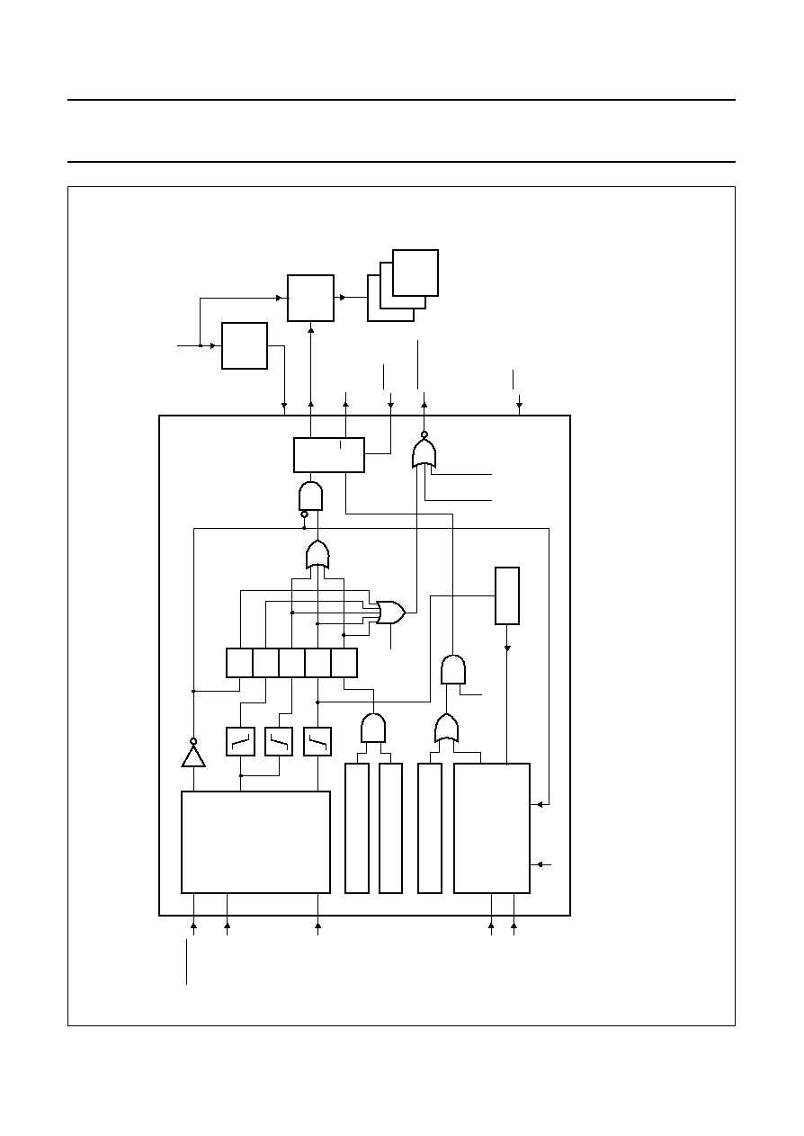
, full pagewidth
LOWVOLT
COMB_INT
RST
RSTO
NPOWON
POWON
DEBOUNCING
T = 62.5 ms
ONKEY
AUXON
TIMEN
DSPEN
MGE288
3
S
POWON
ICs IN MOBILE
VOLTAGE
REGULATORS
supply
voltage
CURRENT TIME
ALARM TIME
Q
R
MR
V
IN
V
OUT
ON
V
IN
V
OUT
other
interrupts
Q
1
0
2
5
bits
HWCTRL_REG
read HWCTRL_REG
HWCTRL_INT
HWCTRL[SWOFF] = 1
T
1 sec
8 sec WATCHDOG/OFF
TIMER EXPIRY
enable
other
sources
retrigger
Wtg/OFF mode
enable retrigger
Fig.7 ON/OFF logic functional diagram.

1996 Oct 29
20
Philips Semiconductors
Objective specification
GSM signal processing IC
PCF5083
8.2.3
OFF T
IMER AND
W
ATCHDOG
T
IMER
The hardware switch-off and Watchdog Timer are used to
power-down the mobile if the System Controller has lost
control for more than 8 seconds.
8.2.3.1
Watchdog Timer
After the reset signal RST is deactivated, the Watchdog
Timer starts to count. If the timer expires after 8 seconds,
the POWON output is set LOW. To prevent this occurring,
the System Controller must restart the timer periodically,
reading register HWCTRL_REG within 8 seconds after the
previous read operation. The Watchdog function is
enabled if DSPEN = TIMEN = LOW. The configuration
DSPEN = TIMEN = HIGH disables the Watchdog Timer.
All other settings are for debugging purposes.
8.2.3.2
OFF Timer
After the switch-off request (HWCTRL_INT activated via
LOWVOLT or ONKEY conditions), the OFF-Timer starts to
count. If the timer expires after 8 seconds, or if the System
Controller sets HWCTRL_REG[SWOFF] to a logic 1, the
POWON output is set LOW. The OFF-Timer cannot be
restarted with a read access to register HWCTRL_REG.
For some special purposes, e.g. if the battery charging
control is handled from the System Controller, the
OFF-Timer can be stopped after it was activated from
ONKEY or LOWVOLT. It then resumes its watchdog
function. The OFF-Timer is stopped with a write access to
register STOP_REG. The data value written to this register
has to be A5H. Other data values do not stop the
OFF-Timer.
It should be noted that:
·
The OFF/Watchdog Timer is not restarted after a stop
operation
·
If either the ONKEY or LOWVOLT line stays active after
a stop operation, it is again recognized after its 1 second
switch-off time-out or 62.5 ms debouncing period,
respectively.
8.3
Timing Generator
The Timing Generator provides TDMA timing and
power-down signals for the RF transmitter, RF receiver,
synthesizer and baseband interface IC.
The Timing Generator has three modes of operation to
control the mobile:
1. Normal mode: in this mode the mobile is fully active.
All ICs receive their operating voltage, the power
consumption is reduced by switching the ICs on and
off with their power-down inputs.
2. Sleep or Idle mode: in this mode the mobile is
switched on, but no call is active. The mobile will be
fully activated if a mobile originated call is requested
via the keyboard. Otherwise parts of the mobile are
activated from time to time to monitor incoming calls.
Outside these intervals all ICs can be switched off
under control of the PCF5083. In this mode the main
13 MHz clock is switched off. To maintain TDMA
timing alignment, the PCF5083 is running temporarily
on a slower clock frequency.
3. Reduced Sleep mode: this mode is equal to the
Sleep mode, except that the TDMA timing alignment is
maintained by the main 13 MHz clock.
In this chapter the following definitions are used:
·
1 bit (Bit) = 48
×
s = 3.692
µ
s (
TDMA
frame)
·
1 quarterbit (QB) =
1
/
4
Bit = 0.923
µ
s (
TDMA
frame)
·
1 timeslot (TS) = 625 QB = 0.576 ms (
1
/
8
TDMA frame)
·
1 Burst = 1 TS
The term frame refers to a TDMA frame throughout this
section unless otherwise stated.
The Timing Generator consists of:
·
The quarterbit counter (QBC) counting 5000 quarterbit
steps in one TDMA frame and running on 1.0833 MHz.
This clock is switched off during Sleep mode.
·
The Timing Generator (TG) with output polarity and
mask registers.
·
The sleep quarterbit counter (SQBC).
·
The Sleep mode timing generator.
1
13000000
--------------------------
1
1250
-------------
1
5000
-------------
1996 Oct 29
21
Philips Semiconductors
Objective specification
GSM signal processing IC
PCF5083
8.3.1
T
HE
Q
UARTERBIT
C
OUNTER
The quarterbit counter (QBC) represents the timebase of
the mobile. It consists of a 13-bit upcounter. The counter
directly counts the quarterbit steps within one TDMA
frame. Its range is therefore 0 to 4999.
At the beginning of every TDMA frame (quarterbit counter
state 0) the signal FRAME_INT goes LOW, generating an
interrupt (frame interrupt) to the System Controller. The
interrupt line is deactivated by accessing the register
MODE0_REG. The frame interrupt is disabled with
MODEx_REG[DISFRAMEINT] = 1.
8.3.1.1
Initial Quarterbit Counter Timing Alignment
The timing offset between a base station and a mobile
station can be corrected by presetting the quarterbit
counter with an estimated correction value. Therefore the
register QBC_REG has to be set up with this correction
value in frame N and the flag QBRCTRL_REG[SYNC] has
to be set.
At the end of frame N the quarterbit counter is loaded from
QBC_REG with zeros. The duration of frame N + 1 is
5000
-
[QBC_REG] and the mobile will be synchronised at
the beginning of frame N + 2. The frame interrupt at the
beginning of frame N + 1 is disabled. The timing
generation is disabled during frame N + 1. The SYNC flag
is cleared after synchronization.
For the System Controller the resulting timing looks like
frame N being extended and synchronization being
achieved with frame N + 1.
8.3.1.2
Maintaining the Quarterbit Counter Timing
Alignment
Small timing corrections can be made by inserting or
extracting one quarterbit step at the beginning of a TDMA
frame. Therefore the INSERT or EXTRACT flag in register
QBCCTRL_REG have to be set. These flags are cleared
after the timing alignment was performed.
8.3.2
N
ORMAL MODE
In Normal mode the Timing Generator provides the output
signals specified in Table 8.
The power-down signals NPDTX2, NPDTX1 and
NPDBIAS are active LOW by default. All other signals are
active HIGH by default. Active HIGH in this context means
that the signals are on high level during a receive or a
transmit burst.
The output polarity can be changed by setting the
corresponding bit in register POL_REG to a logic 1. The
signals can be clamped to a level depending on their flag
in POL_REG by setting the corresponding bit in register
MASK_REG to a logic 0.
After a reset with RST, the receiver, transmitter and
synthesizer control lines are set to their inactive level.
The general MS timing is assumed to have the receive
timeslot (RX) in timeslot 0, the transmit timeslot (TX) in
timeslot 3 and the monitor timeslot (MON) in timeslot 6
within a TDMA frame.
Table 8
Output signals
SIGNAL
DESCRIPTION
Signals for the receiver section
RXON
baseband interface IC receiver enable
BEN
baseband interface IC enable
PDRX1
receiver power-down 1
PDRX2
receiver power-down 2
Signals for the transmitter section
TXON
baseband interface IC transmitter enable
BEN
baseband interface IC enable
TXKEY1
power amplifier power-down
TXKEY2
power ramping controller trigger signal
PDTX1
transmitter power-down 1
NPDTX1
inverted output of PDTX1
NPDTX2
transmitter power-down 2
PDPIAS
power amplifier bias voltage power-down
NPDBIAS
inverted output of PDBIAS
Signal for the synthesizer
PDSYN
synthesizer power-down

1996 Oct 29
22
Philips Semiconductors
Objective specification
GSM signal processing IC
PCF5083
8.3.2.1
Receiver Timing
The Receiver Timing is characterized in Table 9. The start and duration times are defined by loading the mentioned
registers.
Table 9
Receiver Timing (note 1)
Notes
1. A minimum delay of 948 quarterbit periods must be programmed between the end of a monitor burst and the start of
the next monitor burst, measured from the falling edge of RXON to the next rising edge of RXON.
2. If (MONSTART_REG + 929) > 5000 then the monitor burst ends in the next TDMA timeslot at (MONSTART_REG
+ 929)
-
5000.
3. MODEx_REG[RECRX] enable the generation of Rx burst timing.
4. RXBURSTx_REG (x = 0 to 2) is selected with 2 flags in register MODEx_REG.
5. PDRX1 is not activated during a monitor burst if the MODEx_REG[RXCAL] flag is set.
6. For the three level measurement mode, a second monitor burst can be generated during the TX timeslot. The start
position of this burst is then controlled with register TXSTART_REG. Its duration is given from the same register as
for the actual monitor burst.
7. If (MONSTART_REG + 929 +RXBURSTx_REG) > 5000 then the monitor burst ends in the next TDMA timeslot at
(MONSTART_REG + 929 + RXBURSTx_REG)
-
5000.
8. MODEx_REG[RECMON] enable/disable the generation of monitor burst timing.
BURST TYPE
SIGNAL
START (QB)
(2)
DURATION (BIT)
Rx burst
(3)(4)
RXON
RXSTART_REG + 929 = (0 to 127) + 929
RXLENGTHx_REG = (1 to 255)
BEN
RXSTART_REG + 928 = (0 to 127) + 928
RXLENGTHx_REG + 4 = (1 to 255) + 4
PDRX1
(5)
RXSTART_REG + 1024
-
PDRX1_REG
×
32 =
(0 to 127) + 1024
-
(0 to 31)
×
32
to end of RXON
PDRX2
RXSTART_REG + 1024
-
PDRX2_REG
×
32 =
(0 to 127) + 1024
-
(0 to 31)
×
32
to end of RXON
PDSYN
RXSTART_REG + 1024
-
PDSYN_REG
×
32 =
(0 to 127) + 1024
-
(0 to 31)
×
32
to end of RXON
MON burst
(6)(7)(8)
RXON
MONSTART_REG + 929 = (0 to 4999) + 929
RXLENGTHx_REG = (1 to 255)
BEN
MONSTART_REG + 928 = (0 to 4999) + 928
RXLENGTHx_REG + 4 = (1 to 255) + 4
PDRX1
(5)
MONSTART_REG + 1024
-
PDRX1_REG
×
32 =
(0 to 4999) + 1024
-
(0 to 31)
×
32
to end of RXON
PDRX2
MONSTART_REG + 1024
-
PDRX2_REG
×
32 =
(0 to 4999) + 1024
-
(0 to 31)
×
32
to end of RXON
PDSYN
MONSTART_REG + 1024
-
PDSYN_REG
×
32 =
(0 to 4999) + 1024
-
(0 to 31)
×
32
to end of RXON
1996 Oct 29
23
Philips Semiconductors
Objective specification
GSM signal processing IC
PCF5083
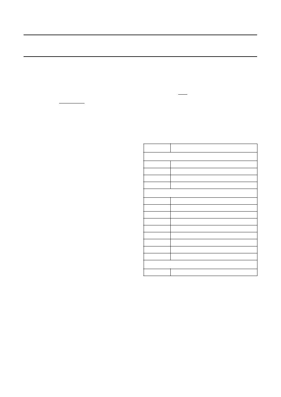
Fig.8 Receiver timing.
handbook, full pagewidth
MGE290
MONSTART_REG
+
929
TXSTART_REG
+
929
RXSTART_REG
+
929
1
16
1
16
RXBURSTx_REG
×
4
MONBURSTx_REG
×
4
MONBURSTx_REG
×
4
(PDRX1_REG
-
3)
×
32
(PDRX1_REG
-
3)
×
32
(PDRX2_REG
-
3)
×
32
(PDRX2_REG
-
3)
×
32
(PDSYN_REG
-
3)
×
32
(PDSYN_REG
-
3)
×
32
3rd level measurement
RX calibration
timing
RXON
BEN
PDRX1
PDRX2
PDSYN
5000
FRAME_INT
RX
(TX)
MON

1996 Oct 29
24
Philips Semiconductors
Objective specification
GSM signal processing IC
PCF5083
8.3.2.2
Transmitter Timing
The transmitter timing is shown in Table 10. The start and duration times are defined by loading the named registers.
Table 10 Transmitter Timing
Notes
1. The timing advance is adjusted with the value of TXSTART_REG.
2. TXBURSTx_REG and TXKEYx_REG (x = 0 or 1) is selected with a flag in register MODEx_REG.
3. Therefore (N)PDBIAS will always be active at least 4
×
32 QB prior to PDTX1.
BURST TYPE
SIGNAL
START (QB)
(1)
DURATION (QB)
(2)
TX burst
TXON
TXSTART_REG + 929 = (0 to 2047) + 929
TXLENGTHx_REG = (1 to 255)
BEN
TXSTART_REG + 928 = (0 to 2047) + 928
to end of TXON + 16
(N)PDTX1,2
TXSTART_REG + 1024
-
PDRX1,2_REG
×
32 =
(0 to 2047) + 1024
-
(0 to 31)
×
32
to end of TXKEY + PDDELAY_REG
(1 to 63)
(N)PDBIAS
TXSTART_REG + 1024
-
PDBIAS_REG
×
32 =
(0 to 2047) + 1024
-
(0 to 31)
×
32
or if PDBIAS_REG < PDTX1_REG + 4 (note 3):
TXSTART_REG + 1024
-
(PDTX1_REG + 4)
×
32
= (0 to 2047) + 1024
-
(0 to 31)
×
32
to end of
TXKEY + PDDELAY_REG + 32 (1 to 63)
TXKEY1
TXSTART_REG + 929 + KEYON1_REG =
(0 to 2047) + 929
+
(1 to 511)
×
32
TXKEYx_REG = (1 to 1023)
TXKEY2
TXSTART_REG + 929 + KEYON2_REG =
(0 to 2047) + 929
+
(1 to 511)
×
32
to end of TXKEYx + KEYOFF_REG
(1 to 63)
PDSYN
TXSTART_REG + 1024
-
PDSYN_REG
×
32 =
(0 to 2047) + 1024
-
(1 to 31)
×
32
to end of TXKEYx + PDDELAY_REG
(1 to 63)
1996 Oct 29
25
Philips Semiconductors
Objective specification
GSM signal processing IC
PCF5083
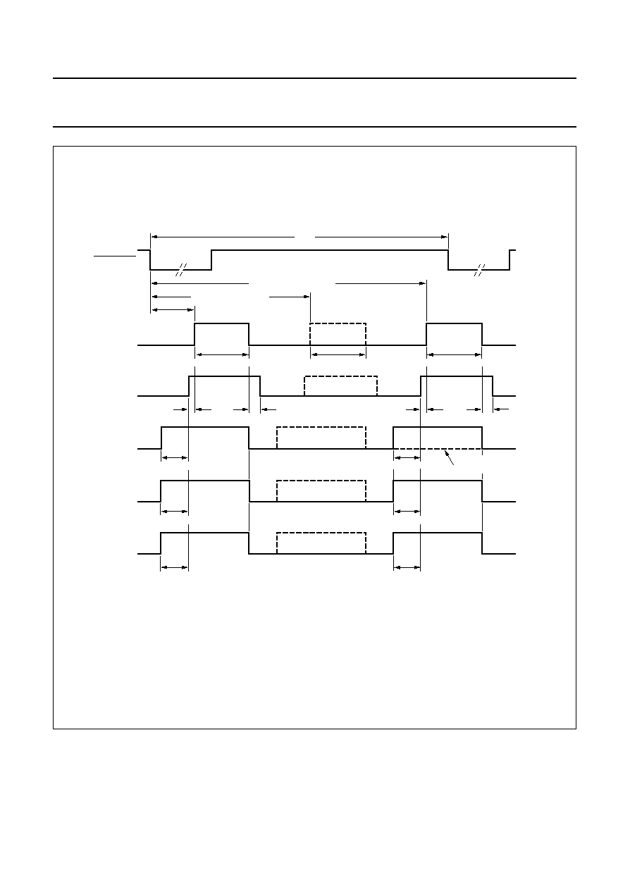
Fig.9 Transmit burst timing.
handbook, full pagewidth
MGE291
32
1
16
5000
TXSTART_REG
+
929
TXBURSTx_REG
×
4
TXKEYx_REG
KEYON1_REG
KEYON2_REG
KEYOFF_REG
(PDTX1_REG
-
3)
×
32
(PDTX2_REG
-
3)
×
32
(PDSYN_REG
-
3)
×
32
(PDBIAS_REG
-
3)
×
32
or
(PDTX1_REG
+
1)
×
32
(see text)
PDDELAY_REG
FRAME_INT
TXON
BEN
TXKEY1
TXKEY2
PDTX1
NPDTX2
PDSYN
PDBIAS

1996 Oct 29
26
Philips Semiconductors
Objective specification
GSM signal processing IC
PCF5083
8.3.2.3
Timing Generation
To generate all burst types required to fulfil the GSM timing, it is necessary to combine and/or modify the basic receive
and transmit burst sequences. For this purpose two registers MODE0_REG and MODE1_REG exist, containing some
flags to control the burst timing. Both mode registers and the registers RXSTART_REG, TXSTART_REG and
MONSTART_REG have an additional pipeline stage.The first register stage can be read or written by the SC.
The second stage is used for timing generation. The pipelining operation is performed at QBC = 0 (together with the
frame interrupt generation). Some flags inside the mode registers have a third pipelining stage to allow the generation of
a MON burst which overlaps into the next frame. The System Controller must set up the registers within the frame before
the programmed timing becomes active. Which register MODE0_REG or MODE1_REG is actually used is described in
Table 11. MODE0_REG and MODE1_REG contain identical flags.
Table 11 Mode Registers (MODE0_REG and MODE1_REG)
Table 12 Register selection for the MON burst
BIT
FLAG
DESCRIPTION
13
USEMODE
MODE_REGx select. If USERMODE = 0; then switch to MODE_REG0 after the next
frame. If USERMODE = 1; then switch to MODE_REG1 after the next frame.
12
DISFRAMENT
Disable frame interrupt. If DISFRAMENT = 1; then the frame interrupt is disabled.
11
RXCAL
RX calibration timing. If RXCAL = 1; then the RX calibration timing is generated.
10
TXLENGTH
Register select. The state of this bit determines which registers are used for the TX
burst. If TXLENGTH = 0; then registers TXBURST0_REG and TXKEY0_REG are
used. If TXLENGTH = 1; then registers TXBURST1_REG and TXKEY1_REG are
used.
9
MONLENGTH1
RXBURSTx_REG select. The state of these two bits determine which RXBURST
register is used for the MON burst; see Table 12.
8
MONLENGTH0
7
RXLENGTH1
RXBURSTx_REG select. The state of these two bits determine which RXBURST
register is used for the Rx burst; see Table 13.
6
RXLENGTH0
5
DTX
DTX timing enable. If DTX = 1; then DTX timing is enabled.
4
SEND
TX burst timing. If SEND = 1; the TX burst timing is generated.
3
RECON
Receiver start-up. If RECON = 1, the receiver start-up sequence for the MON burst
in the idle frame is generated.
2
RECMON
MON burst timing. If RECMON = 1; the MON burst timing is generated.
1
RECTX
Third level measurement. If RECTX = 1; then the MON burst timing during the TX
timeslot for a third level measurements generated.
0
RECRX
Rx burst timing. If RECRX = 1; the Rx burst timing is generated.
MONLENGTH1
MONLENGTH0
REGISTER SELECTED
0
0
RXBURST0_REG is used.
0
1
RXBURST1_REG is used.
1
0
RXBURST2_REG is used.
1
1
Undefined during a MON burst.

1996 Oct 29
27
Philips Semiconductors
Objective specification
GSM signal processing IC
PCF5083
Table 13 Register selection for the Rx burst
8.3.2.4
MON burst during idle frame
This burst is a special case of the MON burst. It is used for FCB search and for monitoring during the idle frame. If
RECON is set, a timing equivalent to the MON burst timing is generated, with the exception that all output lines (BEN,
RXON, PDRXx etc.) are kept active at the end of the burst. The output lines are set inactive again during the first frame
with RECMON set at the time, they normally would be deactivated at the end of a MON burst. During the frames in
between, either RECON = 1, or RECRX = RECTX = RECMON = RECON = SEND = 0 must be programmed.
8.3.2.5
Register mode switching
Which of the registers MODE0_REG or MODE1_REG is used for timing generation is determined using the following two
rules:
1. After any write access to MODE0_REG, MODE0_REG is active during the next frame.
2. After every frame the USEMODE flag of the currently active register determines which register is used during the
next frame, unless there was a write access to MODE0_REG during the current frame.
e.g. MODE0_REG: USEMODE = 1 and MODE1_REG: USEMODE = 0 is programmed during frame N.
This causes the following timing:
a) MODE0_REG is active during frame N + 1
b) MODE1_REG is active during frame N + 2
c) MODE0_REG is active during frame N + 3 and so on, until MODE0_REG is being written again.
8.3.2.6
DTX Mode Processing
DTX mode (Discontinuous Transmission) is enabled with MODEx_REG[DTX] = 1. In DTX mode, the DSP makes the
decision whether a TX burst should be generated or not. The DTX condition is signalled via IO4 (generate transmit burst:
IO4 = 0, no transmit burst: IO4 = 1). If no TX burst is to be generated, the power-down lines TXKEY1/2, (N)PDTX1/2 and
PDSYN are kept inactive or if already asserted, they are set inactive again. (N)PDBIAS become inactive with their default
delay of 8 bit after (N)PDTX1/2 respective PDSYN if they were already asserted, otherwise they also remain inactive.
TXON and BEN are not affected from DTX mode.
8.3.2.7
Interface to the RF-IC Bus
The Timing Generator provides trigger signals for the frequency and gain control channels of the RF-IC interface when
the quarterbit counter matches either RXSTART_REG, TXSTART_REG or MONSTART_REG. Further trigger signals
are generated for the gain control channel after every receive burst to send the contents of register DACOFF_REG and
prior to a receive burst if the quarterbit counter matches xxSTART_REG + 1024
-
AGCSTART_REG
×
32 (xx = RX, TX
or MON) to send the contents of register DACON_REG (refer to Section 8.4).
Note, if the generation of a trigger signal falls into an active burst, the trigger signal is delayed until the end of the current
burst.
RXLENGTH1
RXLENGTH0
REGISTER SELECTED
0
0
RXBURST0_REG is used.
0
1
RXBURST1_REG is used.
1
0
RXBURST2_REG is used.
1
1
Undefined during a RX burst.

1996 Oct 29
28
Philips Semiconductors
Objective specification
GSM signal processing IC
PCF5083
8.3.2.8
Timing modes Application Examples
Table 14 Timing mode applications
Note
1. The SYNC burst location is defined by MONSTART_REG. If a timing is required with s = MONSTART_REG
5000,
MONSTART_REG is programmed with s mod 5000 and the second alternative is used.
FRAME
4
3
2
1
0
BIT ASSIGNMENT;
REGISTER MODE_REG
SEND
RECON RECMON RECTX
RECRX
ACTION
BCCH Detection
N
0
1
0
0
0
Receiver on at the start of timeslot 0
(MONSTART_REG = 0) in TDMA frame N + 1.
Receiver on.
N + 1 to N + M
0
0
0
0
0
Keep receiver on.
N + 1 + M
0
0
1
0
0
Receiver off after number of samples defined
by MONSTART_REG, RXLENGTHx_REG and
number of TDMA frames M.
Frequency Estimation
X
0
0
0
0
1
Receive during TS0.
Frame with RX, TX, MON
X
1
0
1
0
1
Receive during RX, MON, transmit during TX.
Frame before idle frame (monitoring)
I-1
1
1
0
0
1
Receive during RX, transmit during TX, receiver
on defined by MONSTART_REG.
Idle frame (monitoring)
I
0
0
1
0
0
Receiver off defined by MONSTART_REG and
RXLENGTHx_REG.
Frame with RX, TX, MON
I-1
or
(1)
1
0
1
0
1
Receive during RX, MON, transmit during T.
I-1
1
0
0
0
1
Receive during RX, transmit during TX.
Idle frame (SYNC burst reading)
I
or
(1)
0
0
0
0
0
No operation.
I
0
0
1
0
0
Receive during MON.
Three level measurements
X
0
0
1
1
1
Receive during RX, TX and MON slot.
Send access burst
X
1
0
0
0
0
Transmit during TX.

1996 Oct 29
29
Philips Semiconductors
Objective specification
GSM signal processing IC
PCF5083
During the three level measurement mode the burst length
of the receive burst during the TX slot is defined by the
same register RXBURSTx_REG as used for the
MON burst. The receive frequency must be set by
programming the TX channel of the RF_IC interface.
For a certain operation mode in frame N, the Timing
Generator has to be programmed with all necessary
parameters in frame N
-
1. For this purpose the registers
RXSTART_REG, TXSTART_REG, MONSTART_REG
and MODEx_REG have an additional pipelining stage.
The pipelining takes place at the beginning of every TDMA
frame with the frame interrupt generation.
8.3.3
S
LEEP MODE
The Sleep mode circuitry is used to reduce the power
consumption during the Idle mode. During Sleep mode,
the mobile is switched on, but no call is active. The mobile
is only activated to read the paging blocks and for
neighbour cell monitoring. Outside these intervals, all ICs
can be switched off to save power.
In this mode also the main 13 MHz oscillator may be
switched off. To maintain TDMA timing alignment, the
PCF5083 is running temporarily on a slower clock
frequency, derived from the 32.768 kHz real time clock
oscillator. This clock is called Sleep Clock (SLCLK).
During the Sleep mode the PCF5083 controls the signals
specified in Table 15, the timing for these signals is
detailed in Table 16.
Sleep mode is activated with
QBCCTRL_REG[SLEEP] = 1 and
QBCCTRL_REG[SLEEPRED] = 0 (the SLEEPRED flag is
used for reduced Sleep mode, see below). The register
SLEEPCNT_REG has to be programmed with the number
of TDMA frames the mobile wants to sleep minus one.
Register FRAMECNT_REG is automatically cleared when
the Sleep mode is entered and counts the number of
TDMA frames actually slept. The 9-bit registers
SLEEPCNT_REG and FRAMECNT_REG allow a
maximum Sleep mode period of 512 frames. Refer to
Fig.11 for the signal flow.
Table 15 Signals controlled by the PCF5083 during Sleep mode
Table 16 Sleep mode signal timing
Notes
1. (N)REFON is not deactivated if the Sleep mode is initiated while the sleep clock calibration procedure is running (see
Section 8.3.3.3), while the IOM
®
-2 interface is enabled or the MMICLK flag in register HWCTRL_REG is set,
indicating that the MMI controller requires the 13 MHz clock.
2. Maximum 295 ms before Sleep mode terminates with 4.6 ms resolution {[(0 to 63) + 1]
×
4.6 ms}.
SIGNAL
DESCRIPTION
REFON
Reference oscillator on. Active HIGH output.
NREFON
Inverted REFON output.
DSPON
DSP power-down (connected on chip).
GPON1
General purpose power-down and radio part interface 3-state enable. Active HIGH output.
GPON2
General purpose power-down. Active HIGH output.
SIGNAL
FRAME NUMBER
ACTIVATION OF SIGNAL IF
SLEEPCNT_REG EQUALS
(N)REFON
In frame N + 1 on the third positive SLCLK edge
REFON_REG (notes 1 and 2)
DSPON
In frame N + 1 on the second positive SLCLK edge
KISSON_REG (note 2)
GPON1
In frame N + 1 on the second positive SLCLK edge
GPON1_REG (note 2)
GPON2
In frame N + 1 on the third positive SLCLK edge
GPON2_REG (note 2)
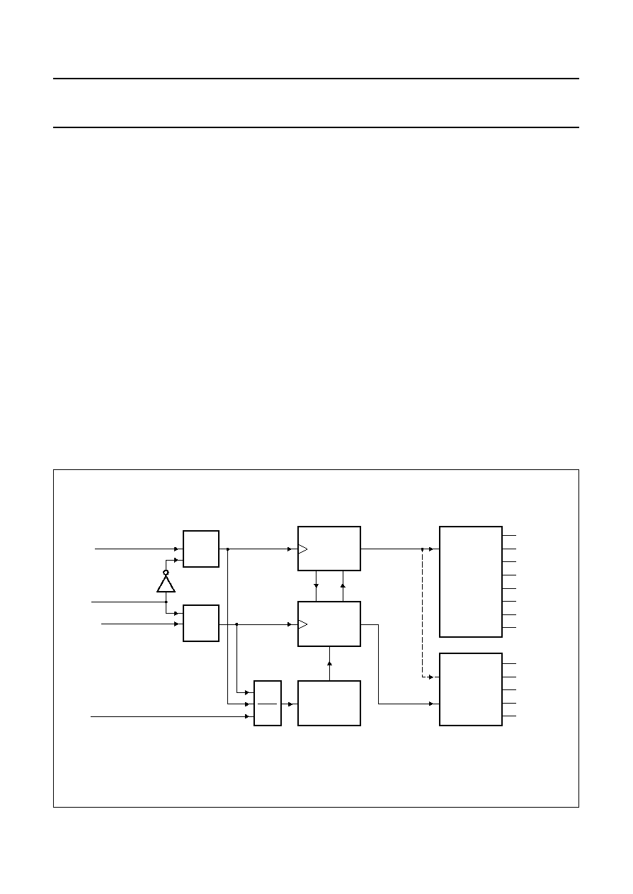
1996 Oct 29
30
Philips Semiconductors
Objective specification
GSM signal processing IC
PCF5083
A power-down line is only deactivated during Sleep mode
if the corresponding activation register is programmed with
a higher value than register SLEEPCNT_REG. Otherwise
the power-down line stays active during Sleep mode. The
output polarity of the power-down lines can be changed by
setting their corresponding bit in register POL_REG to a
logic 1. The signals can be clamped to a level depending
on their flag in POL_REG by setting the corresponding bit
in register MASK_REG to a logic 0.
Because the 13 MHz clock is also internally disabled
during Sleep mode, the PCF5083 cannot be accessed
with the host port.
During Sleep mode, burst timing and frame interrupt
generation is stopped and the registers MODE0_REG and
MODE1_REG are cleared.
8.3.3.1
Transceiver control lines
The timing generator signals RXON, TXON, BEN, PDRX1,
PDRX2, PDTX1, NPDTX1, NPDTX2, PDBIAS, NPDBIAS,
PDSYN, TXKEY1, TXKEY2 and the RF device control bus
signals RFCLK, RFDO, RFEN1 to RFEN4, RFE and the
Voice Port signals ASF, ACLK and ADO are 3-stated as
long as the signal GPON1 is inactive during Sleep mode.
The signals are driven into their high-impedance state
independently of the actual polarity to which GPON1 is
programmed, unless MASK_REG[GPON1] = 0. In this
case the outputs are driven during Sleep mode.
8.3.3.2
The Sleep Quarterbit Counter
In Sleep mode, the 13 MHz reference oscillator is switched
off to reduce the power consumption. The TDMA timing is
maintained using the sleep quarterbit counter (SQBC),
which is driven from the sleep clock (SLCLK). The sleep
clock is derived from the 32.768 kHz real time clock. Upon
entering Sleep mode, the contents of the quarterbit
counter are copied to the sleep quarterbit counter. After
the end of a Sleep mode period, the sleep quarterbit
counter is copied back to the quarterbit counter and normal
timing is performed again.
To maintain the correct timing over hundreds of TDMA
frames, the sleep quarterbit counter is incremented with
the value SQBC_INC equal to the clock ratio between the
quarterbit clock and the sleep clock. This value must be
very accurate and can be derived using the calibration
method described in Section 8.3.3.3.
Fig.10 Quarterbit counters for normal and Sleep mode.
handbook, full pagewidth
MGE289
QBCCTRL_REG[SLEEP]
QBCCTRL_REG[CAL]
13 MHz
1.08325 MHz
32768 Hz
SLCLK
8192 Hz
EN
÷
4
÷
12
QBC
(0 to 4999)
TIMING
GENERATOR
NORMAL
MODE
SQBC
RXON
Enter normal mode:
Copy SQBC to QBC
reduced
sleep
mode
Enter sleep mode:
Copy QBC to SQBC
SQBC_INC
(0 to 255)
typ. 123
1083
8.192
EN
TXON
BEN
PDRX1,2
(N)PDTX1,2
SYNON
(N)PDBIAS
TXKEY1,2
TIMING
GENERATOR
SLEEP
MODE
GPON1
GPON2
DSPON
REFON
NREFON
+

1996 Oct 29
31
Philips Semiconductors
Objective specification
GSM signal processing IC
PCF5083
8.3.3.3
Sleep Clock Calibration
Since the ratio between the quarterbit clock and the sleep
clock may vary, an accurate value for the increment
SQBC_INC can be obtained with the following procedure:
1. Set QBCCTRL_REG[CAL] = 1 to enable the
calibration mode.
2. The calibration procedure lasts for 8 seconds.
3. After calibration, the CAL flag in QBCCTRL_REG is
automatically cleared. After 1 ms the register
SQBCINC_REG holds the lower 8 bits of the
increment value and can be used to verify the
calibration process. The maximum allowed frequency
deviation is
-
23.8 kHz to +25.4 kHz at 13 MHz and
-
63.6 Hz to +60.3 Hz at 32.768 kHz.
During the calibration procedure, the 13 MHz master clock
may not be switched off. Therefore, REFON stays active
even if the Sleep mode is enabled.
The calibration procedure has to be repeated from time to
time, because the exact frequency of the 13 MHz as well
as the 32 kHz clock may change.
After power up, the calibration procedure must be
performed before the Sleep mode can be activated.
8.3.3.4
Reduced Sleep mode
During reduced Sleep mode the mobile timing is
maintained with the quarterbit counter. The sleep
quarterbit counter is not used. For the System Controller
all timings are as in Sleep mode. The signal REFON is
always active. All other Sleep mode signals (GPON1 etc.)
are activated as during Sleep mode. The reduced Sleep
mode is invoked with QBCCTRL_REG[SLEEP] = 1 and
QBCCTRL_REG[SLEEPRED] = 1.
8.3.3.5
From Sleep mode to Normal mode
The PCF5083 is forced into a wake-up state if the
hardware control interrupt HWCTRL_INT is asserted
internally (caused by the ON/OFF monitor, MMI
power-down unit or real time clock). The interrupt line
COMB_INT is not asserted but the interrupt stays pending
internally until Sleep mode is finished.
If the PCF5083 enters the wake-up state and
SLEEPCNT_REG is less than or equal to REFON_REG,
the Sleep mode terminates normally. Otherwise, if
SLEEPCNT_REG is greater than REFON_REG,
REFON_REG is copied to SLEEPCNT_REG instead of
SLEEPCNT_REG being decremented at the next frame
boundary and the Sleep mode terminates with reduced
duration. The maximum delay from any wake-up request
to the end of the wake-up procedure depends on the
setting of REFON_REG and is 64
×
4.6 ms = 294.4 ms.
After entering the normal mode again FRAMECNT_REG
shows the number of actually slept frames. If the Sleep
mode terminated normally, this number equals the number
SLEEPCNT_REG previously was programmed with.
The System Controller now has to set up the timing
generator mode for the next frame. With the beginning of
the next frame the PCF5083 enters the normal operation
again.
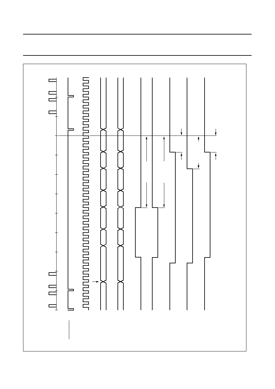
1996 Oct 29
32
Philips Semiconductors
Objective specification
GSM signal processing IC
PCF5083
handbook, full pagewidth
MGE292
TDMA FRAME
FRAME_INT
SLCLK
SLEEPCNT_REG
FRAMECNT_REG
NREFON
REFON
DSPON
GPON1
GPON2
N
-
1NN
+
1N
+
2N
+
3N
+
4N
+
5N
+
6N
+
7
N
+
8
N
+
9N
+
10
REFON_REG
REFON_REG
DSPON_REG
GPON2_REG
GPON1_REG
set QBCCTRL[SLEEP] = 1
set SLEEPCNT_REG = 7
RX
MON
RX
MON
RX
MON
RX
MON
X
X
7
0
6
1
5
2
4
3
3
4
2
5
1
6
0
7
Fig.11 Sleep mode timing.

1996 Oct 29
33
Philips Semiconductors
Objective specification
GSM signal processing IC
PCF5083
8.4
RF-IC Interface Bus
This block provides a serial interface to control the RF
devices like synthesizer, baseband interface IC etc. The
interface is upward compatible with the `Philips Three Wire
Bus'. Compared with the Philips bus it is extended for
bidirectional data transfer and additional timing modes are
implemented. The interface consists of a clock (RFCLK), a
data output (RFDO), a data input (RFDI) and enable lines
(RFEN1 to RFEN4 and RFE). The interface is subdivided
into three logical channels as described below.
8.4.1
F
REQUENCY
S
ETTING
C
HANNEL
The registers RX_REG, TX_REG and MON_REG are set
up during frame N
-
1 with the frequency information for
the RX, TX or MON burst of frame N. Therefore these
three registers have a pipeline stage. The pipelining takes
place at the beginning of every TDMA frame together with
the frame interrupt generation. The transmission of the
three registers is controlled from the timing generator as
described in Section 8.3.2.7. The register TX_REG is also
used for a monitor burst during the TX timeslot. The
register RFCTRL0_REG contains four address bits
(A0 to A3) which are transmitted with either of the three
data registers. The data structure and the function of the
mode (M0 to M2) and select (SEL0, SEL1) flags contained
in RFCTRL0_REG is described in Section 8.4.4.
8.4.2
G
AIN
C
ONTROL
C
HANNEL
The registers RXGAIN_REG, TXGAIN_REG and
MONGAIN_REG are set up during frame N
-
1 with the
gain control information for the RX burst or MON burst of
frame N. Therefore these three registers have a pipeline
stage. The pipelining takes place at the beginning of every
TDMA frame together with the frame interrupt generation.
The transmission of the three registers is controlled from
the timing generator as described in Section 8.3.2.7. No
gain information is sent prior to a TX-burst. The register
TXGAIN_REG is used for a monitor burst during the TX
timeslot. The DAC bit of these registers is not transmitted
but used to select between the registers DAC0_REG and
DAC1_REG. The register RFCTRL1_REG contains four
address bits (A0 to A3) which are transmitted with either of
the three data registers. The data structure and the
function of the mode (M0 to M2) and select
(SEL0 and SEL1) flags contained in RFCTRL1_REG is
described in Section 8.4.4.
The DAC flag in xxGAIN_REG selects either DAC0_REG
or DAC1_REG to be transmitted immediately after
xxGAIN_REG. These two registers hold static data and do
not have an additional frame pipeline stage like the
xx_REG or xxGAIN_REG. The contents of register
RFCTRL2_REG functionally corresponds to the contents
of RFCTRL1_REG.
Two further registers, DACON_REG and DACOFF_REG
exist. They are used to power-up or power-down a gain
setting DAC. These two registers also hold static data like
DACx_REG. The transmission of the three registers is
controlled from the timing generator as described in
Section 8.3.2.7. The contents of RFCTRL3_REG register
functionally corresponds to the contents of
RFCTRL1_REG or RFCTRL2_REG.
The MSB (bit 16) of the registers DAC0_REG,
DAC1_REG, DACON_REG and DACOFF_REG is located
in register MSB_REG, because of the limited address
space.
8.4.3
I
MMEDIATE
C
ONTROL
C
HANNEL
The Immediate Control Channel (IMC) consists of the
registers IMCOUT_REG for the output direction and
IMCIN_REG for the input direction. The contents of
IMCOUT_REG are transmitted every time a new data
word is written to it. The flag SIINT_REG[IMC_OBE] is set
after the contents of IMCOUT_REG was copied to the shift
register. If the corresponding mask flag
SIMASK_REG[IMC_OBE_MASK] is set, the serial
interface interrupt SI_INT is activated. Together with
IMCOUT_REG being transmitted, the data at RFDI is read
into register IMCIN_REG. The flag SIINT_REG[IMC_IBF]
is set at the end of the shift operation. The interrupt
handling corresponds to the IMC_OBE flag. The interrupt
flags are cleared when their corresponding register is
written respectively read.
The mode flags in IMCOUT_REG have the same function
as the flags in RFCTRLx_REG. The four select flags
(SEL0 to SEL3) correspond to the enable lines
RFEN1 to RFEN4. Each enable line is activated if their
corresponding select flag is set. Therefore it is possible to
activate more than one line at a time.
1996 Oct 29
34
Philips Semiconductors
Objective specification
GSM signal processing IC
PCF5083
Table 17 Select flags in register IMCOUT_REG
The inhibit flag (INH) in IMCOUT_REG controls whether
the IMC operation is inhibited during a receive or transmit
burst indicated with PDRX2 or NPDTX2 active. If the INH
flag is set the IMC operation is delayed until PDRX2 and
NPDTX2 become inactive. If the INH flag is reset the two
lines are don't care.
8.4.4
O
PERATION
M
ODES AND
C
ONTROL
R
EGISTERS
The characteristics of each channel are controlled using
the contents of the registers RFCTRL0_REG to
RFCTRL3_REG.
The interface is programmable, one of three timing modes
can be selected for every data transfer. For the exact
timing see Chapter 16. In Mode 3 the transmission of the
data registers associated with the control register is
disabled.
If there is a conflict between the different data channels,
data transmission is scheduled according to Table 22.
Table 18 RC-IF Interface Bus Control Registers
SEL0 SEL1 SEL2 SEL3
ACTIVE ENABLE LINE
1
X
X
X
RFSEN1
X
1
X
X
RFSEN2
X
x
1
X
RFSEN3
X
X
X
1
RFSEN4
BIT
FLAG
OPERATION
7
M1
These two bits select the timing
mode, see Table 19.
6
M0
5
SEL1
These two bits are used to assert
the enable lines RFEN1 to RFEN1,
see Table 21.
4
SEL0
3
A3
These four bits form the address
field.
2
A2
1
A1
0
A0
Table 19 Selection of the RC-IF Interface timing modes
Note
1. The 16 or 21 data bits are transmitted MSB first
according to Table 20.
Table 20 RF-IC Interface data structure
Note
1. The 21 bits consist of D17 to D0 and A2 to A0.
Table 21 Selection of enable lines RFEN1 to RFEN4
Table 22 Order of priority
MODE
M1
M0
BITS
TRANSFERRED
RFE
ASSERTED
0
0
0
21
no
1
0
1
21
no
2
1
0
16
yes
3
1
1
Transmission of the corresponding
data registers is disabled.
MODE
BITS
TRANSFERRED
1ST BIT
LAST
BIT
0 and 1
21
(1)
D17
A0
IMC channel
21
D20
D0
2
16
D15
D0
SEL1
SEL0
ENABLE LINE ASSERTED
0
0
RFEN1
0
1
RFEN2
1
0
RFEN3
1
1
RFEN4
PRIORITY
TRANSMISSION
Highest
frequency setting
gain control DACOFF_REG
gain control DACON_REG
gain control xxGAIN_REG then
DACx_REG
Lowest
Immediate Control Channel
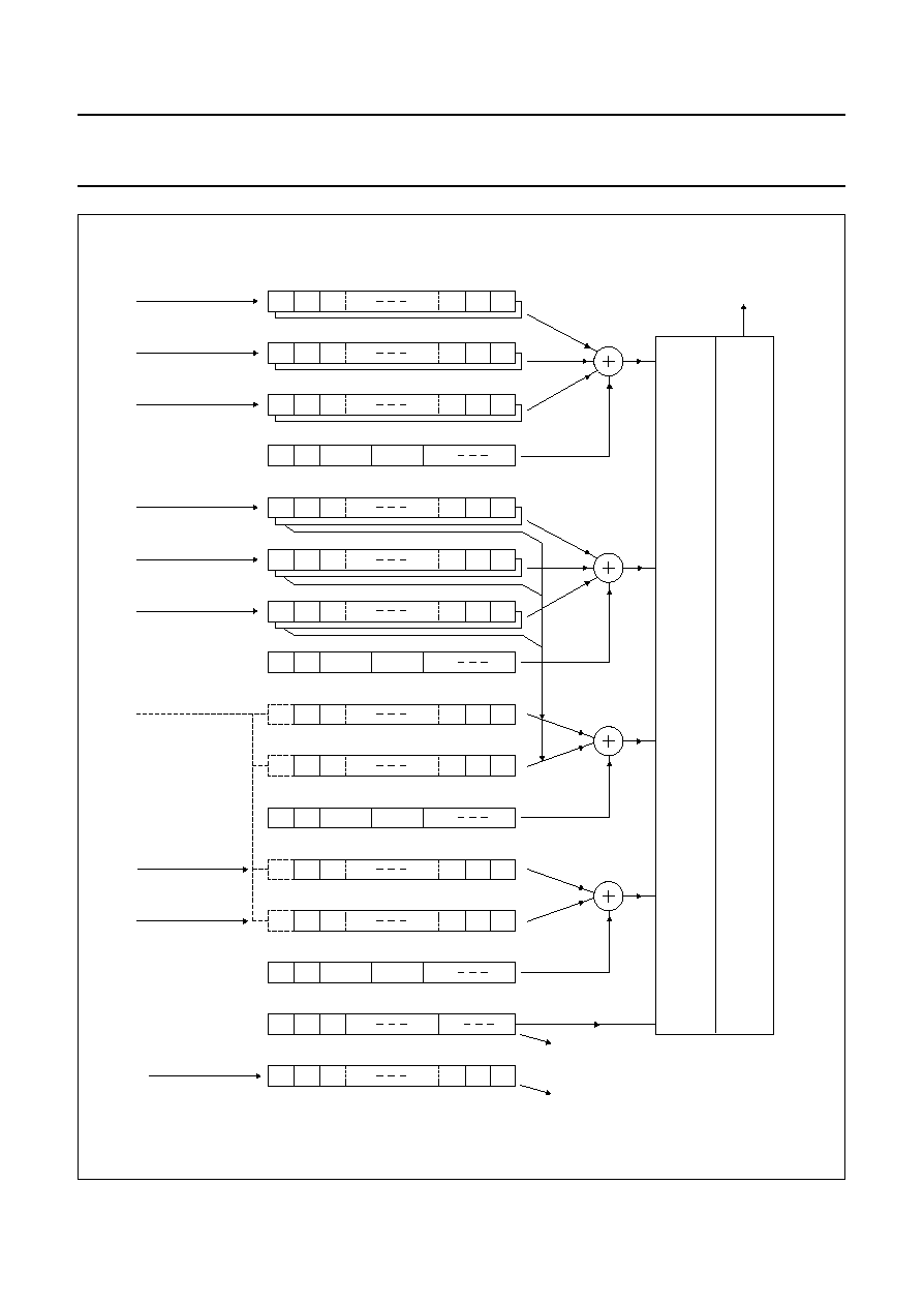
1996 Oct 29
35
Philips Semiconductors
Objective specification
GSM signal processing IC
PCF5083
Fig.12 RF-IC interface register set.
handbook, full pagewidth
D16
QBC = RXSTART_REG
QBC = TXSTART_REG
QBC = MONSTART_REG
RX_REG
D0
RFDO
D16
TX_REG
D0
D16
MON_REG
D0
D20
D0
MGE285
M1
M0
SEL1
SEL0
RFCTRL0_REG
A0
A3
frequency setting channel
gain control channel
immediate control channel
DAC
MUX
SHIFT
REGISTER
QBC = RXSTART_REG
QBC = TXSTART_REG
QBC = MONSTART_REG
RXGAIN_REG
D0
DAC
TXGAIN_REG
D0
QBC matches
ACCSTART_REG
condition
RXON inactive
RFDI
DAC
D16
D16
D16
MONGAIN_REG
D0
MSB_REG
DAC0_REG
D0
D16
DAC1_REG
D0
D16
DACON_REG
D0
SI_INT
+
IMC_OBE flag
SI_INT
+
IMC_IBF flag
D16
DACOFF_REG
D0
D16
M1
M0
SEL1
SEL0
RFCTRL1_REG
A0
A3
M1
M0
SEL1
SEL0
RFCTRL2_REG
A0
A3
M1
M0
SEL1
SEL0
RFCTRL3_REG
A0
A3
INH
M1
M0 SEL3
SEL0
IMCOUT_REG
D0
D20
IMCOUT_REG
TRIGGER
MSB
LSB
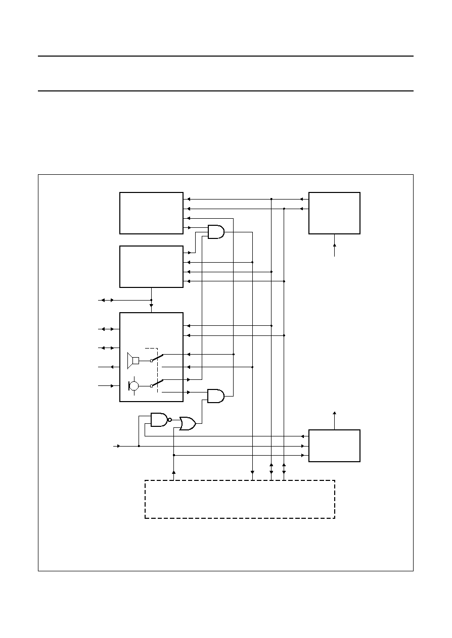
1996 Oct 29
36
Philips Semiconductors
Objective specification
GSM signal processing IC
PCF5083
8.5
IOM
®
-2 Interface
The PCF5083 includes a type of PCM Highway like digital Data and Voice interface which is also available for external
devices. It can be configured to be compatible to the IOM
®
-2 standard. The blocks connected to this bus inside the IC
are the Y-Port of the DSP core, the IOM
®
-2 master and the Audio Interface. The clock and frame synchronization signals
(DCL, FSC) are either generated internally or provided externally. Figure 13 shows the general structure of the IOM
®
-2
interface.
Fig.13 IOM
®
-2 Interface structure.
handbook, full pagewidth
MGE286
DCL
FSC
DCL
FSC
DU
DD
MONITOR / CI
MASTER
UNITS
IOM-2
CLOCK
GENERATION
UNIT
DETECT
NEW
IOM-2 DEVICE
EXTERNAL IOM-2 INTERFACE
FSC
DCL
DD
DU
CLOCK_MODE
SOYD
IO1/AEN
ACLK
AFS
ADO
ADI
SIYD
SIYCLK
SIYEN
IO1
AEN
DSP
CORE
DCL
FSC
B_IN
ACON_REG
A_IN
B_OUT
SI_INT
+
EXT_DVI flag
A_OUT
IOMEXT_EN
AUDIO
INTERFACE

1996 Oct 29
37
Philips Semiconductors
Objective specification
GSM signal processing IC
PCF5083
8.5.1
IOM
®
-2 C
LOCK
G
ENERATION
If the IOM
®
-2 clock and frame synchronization signals are
generated internally from the 13 MHz reference clock, the
basis clock runs at 1.536 MHz as illustrated in Fig.14. One
125
µ
s FSC period consists of 192 DCL periods (0 to 191).
The DCL periods 12, 25, 38, 51, 64, 77, 90, 103, 116, 129,
142, 155, 168 and 181 are 8T wide (high time = low
time = 4T), where T is the 13 MHz clock period
(T = 77 ns). All other DCL periods are 8.5T wide
(high time = 4.5T, low time = 4T).
It is possible to extend or to reduce 12 consecutive IOM
®
-2
frame periods by 1T each. This results in a total reduction
or extension of one quarterbit (12T = 923 ns), which is
required in case of timing alignment. This adjustment is
performed by setting either the FSCEXT flag for extension,
or the FSCRED flag for reduction. Both these flags reside
in QCCTRL_REG. The flags are automatically reset after
the adjustment.
The length of the frame synchronization pulse (FSC) is
chosen to 29
×
8.5T + 2
×
8T + 6T = 268.5T.
The whole IOM
®
-2 signal generation is disabled in Clock
mode 0 (see Table 23, default after reset).
In Sleep mode the REFON output stays active to keep the
13 MHz oscillator running as long as the IOM
®
-2 interface
is not disabled (Clock mode 0).
Other clock modes are derived from this mode by
subdividing the 1.536 MHz DCL clock by 2, 3, 4, 6, or 12.
The FSC period is not changed.
In external clock mode the IOM
®
-2 clock and frame
synchronization signal are provided via the DCL and FSC
pins. The DCL clock in this mode is a multiple of 128 kHz
or 256 kHz with a maximum frequency of 2.048 MHz or
4.096 MHz respectively.
In both internal and external clock modes, it is possible to
select between a double clock cycle mode per data bit or
a single clock cycle mode per data bit with the
IOMCON_REG[DATA_MODE] flag. In double clock cycle
mode the data output gets valid with the first rising edge of
DCL and the data input is sampled with the second
negative edge of DCL within a bit period. In single clock
cycle mode the data output gets valid with the rising edge
of DCL and the data input is sampled with the falling edge
of DCL within a bit period. Data is organized in 16-bit
timeslots. The maximum number of timeslots supported is
12 in internal and 16 in external clock mode.
Table 23 lists all possible clock modes.
Table 23 IOM
®
-2 Clock Modes
DCL
FREQUENCY
SINGLE(1)/DOUBLE(2)
CLOCK CYCLE MODE
NUMBER OF
16-BIT TIMESLOTS
DIVISION
RATIO
CLOCK_MODE
FLAGS (DEC.)
DATA_MODE
FLAG
IOM
®
-2 interface off
-
-
-
0
x
1.536 MHz
2
6
1
1
1
1.536 MHz
1
12
1
1
0
768 kHz
1
6
2
2
0
768 kHz
2
3
2
2
1
512 kHz
2
2
3
3
1
512 kHz
1
4
3
3
0
384 kHz
1
3
4
4
0
256 kHz
2
1
6
5
1
256 kHz
1
2
6
5
0
128 kHz
1
1
12
6
0
external clock
n
×
128 kHz
(2.084 MHz max.)
1
n
(n
16)
-
7
0
external clock
n
×
256 kHz
(4.096 MHz max.)
2
n
(n
16)
-
7
1
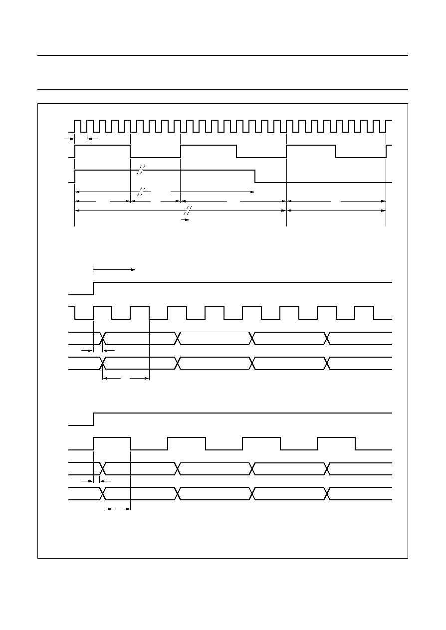
1996 Oct 29
38
Philips Semiconductors
Objective specification
GSM signal processing IC
PCF5083
Fig.14 IOM
®
-2 Interface timing diagrams.
handbook, full pagewidth
MGE293
T
268.5 T
4.5 T
4 T
8.5 T
8 T
DCL periods : 0 to 11, 13 to 24, 26 and 27 182 to 191
DCL periods : 12, 15, 38, 51, 64,
77, 90, 103, 116,
129, 142, 155,
168
(1)
, 181
(1)
,
188
(2)
, 189
(2)
th
tsu
1.536 MHz Basic Clock Scheme (CLOCK_MODE = 1)
Double Clock Cycle Mode (DATA_MODE = 1)
th
tsu
Single Clock Cycle Mode (DATA_MODE = 0)
0
1
2
3
0
1
2
3
0
1
2
3
0
1
2
3
timeslot 0
CLK13
DCL
FSC
FSC
DCL
DD
DU
FSC
DCL
DD
DU

1996 Oct 29
39
Philips Semiconductors
Objective specification
GSM signal processing IC
PCF5083
8.5.2
IOM
®
-2 M
ASTER
U
NIT
The IOM
®
-2 master unit implements two monitor channels
and C/I channel masters. All handshake protocols are
implemented in accordance with the IOM
®
-2 standard with
the exception of the constraints mentioned below. The
data structure of a 16-bit monitor and C/I timeslot is also
implemented according to the IOM
®
-2 standard with the
exception that the timeslot location is not fixed within a
IOM
®
-2 frame.
As data is structured in 16-bit timeslots (see Table 24) the
timeslot a master works on, can be selected with the flags
IOMCON_REG[MASTERx_TS0 to MASTERx_TS3].
These bits binary encode the timeslot number (0 to 5), with
timeslot 0 being indicated with the rising edge of FSC.
Both monitor masters can be independently enabled with
the flags IOMCON_REG[MASTERx_EN].
For every serviced channel a data register (MON0_REG,
MON1_REG, CI0_REG and CI1_REG) with input and
output buffer stage and a state machine for receive and
transmit direction exists. For every register
IOMFLAG_REG holds two flags to indicate the input data
buffer full and the output buffer empty condition. The flags
are xxx_IBF (input buffer full) and xxx_OBE (output buffer
empty) with xxx equal to the register name. If one of these
flags together with the corresponding enable flag in
IOMEN_REG is set the IOM
®
-2 interrupt is activated (refer
to Section 10.2). The flags are reset with read respectively
write operations to their corresponding data register.
8.5.3
M
ONITOR
C
HANNEL
T
RANSMITTER
P
ROTOCOL
·
After IOMCON_REG[MASTERx_EN] is set to a logic 1,
the transmitter state machine is in an idle state. The
pattern FFH is sent and the output buffer empty flag
MONx_OBE (x = 1 or 2) is set. The MX flag is sent as a
logic 1 in accordance with the IOM
®
-2 specifications.
·
To initiate a message transmission the System
Controller has to program MONx_REG with the first byte
of the message. The MONx_OBE flag is cleared with the
data write access.
·
A full handshake is implemented in accordance with the
IOM
®
-2 specifications. The transmitter may delay the
data transmission in case the System Controller does
not provide new data in time. MX = 0 is maintained until
MONx_REG is programmed with new data. The
MONx_OBE flag is cleared with the data write access.
The receiver delays the data transmission if it sends no
data acknowledge. In this case MX = 0 is maintained
and the data byte is repeated in subsequent frames.
·
To request new data from the controller the MONx_OBE
flag may be set as soon as the data acknowledge
(MR = 1) from the receiver is detected except for the first
byte reception. Here the MR transition HIGH-to-LOW
has to be detected. This leaves the controller
approximately 250
µ
s to program the MONx_REG with
the next byte without delay within the handshake
procedure except for the first byte.
·
An end of transmission is sent if the TEOMx flag in
IOMCTRL_REG is set when MONx_OBE = 1 after the
last byte transmission. The end of transmission is sent
(MX = 1 in at least two subsequent frames) after the
acknowledge of the last byte is completely received.
After the end of transmission is sent the transmitter state
machine is in the idle state.
·
The TEOMx flags are also used to initialize the
transmitter state machine. If the flag is set the state
machine may get from any state into the idle state.
·
The TEOMx flag is automatically cleared.
·
If an abort request is received, the transmitter in
accordance with the specifications, sends the end of
transmission sequence and enters the idle state. The
MONx_OBE flag is set. The abort request is indicated
with the RABORTx flag set in IOMCTRL_REG.
RABORTx = 1 also asserts the IOM
®
-2 interrupt
(MONx_OBE_EN is used as enable bit) to indicate the
abort to the System Controller. The flag is reset with the
MONx_OBE flag.
Table 24 Data structure of a 16-bit IOM
®
-2 monitor and C/I master timeslot
15
14
13
12
11
10
9
8
7
6
5
4
3
2
1
0
MONX
C/IX
MR
MX

1996 Oct 29
40
Philips Semiconductors
Objective specification
GSM signal processing IC
PCF5083
8.5.4
M
ONITOR
C
HANNEL
R
ECEIVER
P
ROTOCOL
·
After IOMCON_REG[MASTERx_EN] is set to a logic 1,
the receiver state machine is in an idle state and waits
for the first byte transmission. The input buffer full flag
MONx_IBF is cleared. The MR flag is sent as a logic 1
in accordance with the IOM
®
-2 specification.
·
After the reception of a data byte the MONx_IBF flag is
set and the System Controller may read the data from
MONx_REG.
·
A full handshake is implemented in accordance with
IOM
®
-2 specification. The receiver may delay the data
transmission if the input buffer is full and the System
Controller does not read the buffer in time. In this case
MR = 0 is maintained until MONx_REG is read. The
MONx_IBF flag is cleared with the data read access.
The transmitter may delay the data transmission if it
delays the next byte valid indication. In this case MR = 0
is maintained in subsequent frames.
·
If an end of transmission is detected the receiver state
machine gets into the idle state. The REOMx flag in
IOMCTRL_REG is set. REOMx = 1 also asserts the
IOM
®
-2 interrupt (IOMx_IBF_EN is used as enable bit)
to indicate the end of transmission to the System
Controller. The REOMx flag is cleared with a dummy
read of MONx_REG.
·
To send an abort request the TABORTx flag in
IOMCTRL_REG is set. The receiver state machine
enters the idle state. The TABORTx flag is reset after the
procedure.
Time-outs are not detected. Collision detection and the
maximum speed case is not supported.
8.5.5
C
OMMAND
/I
NDICATION
C
HANNEL
T
RANSMITTER
All data words are sent at least in two subsequent frames.
If the transmitter runs out of data the last data word is
repeated. The flags CI0(1)_IBF and CI0(1)_OBE are
provided to indicate the input/output register status.
8.5.6
C
OMMAND
/I
NDICATION
C
HANNEL
R
ECEIVER
If the received data is different from the data input buffer
the new data pattern is loaded into the data input buffer.
The CI0(1)_IBF flag is cleared if it is set. If during the next
frame the received data is identical to the data stored in the
data input buffer the buffer contents is considered valid
and the CI0(1)_IBF flag is set. The System Controller now
has to fetch the data within the next 125
µ
s, otherwise data
might be lost.
8.5.7
A
UDIO
I
NTERFACE
The Audio Interface provides the translation of one 16-bit
IOM
®
-2 timeslot into a timing according to Chapter 16 for
the receive and transmit direction. The operation of the
interface is configurable with the flags of register
ACON_REG. The Audio Interface is enabled or disabled
under control of the DSP core with IO1/AEN = 1.
Otherwise the data word 00H is sent in both directions.
With ACON_REG[TRANS_EN] = 1, a transparent mode is
selected. In this mode the internal IOM
®
-2 signals FSC
and DCL are directly connected to ACLK and AFS. ADI is
directly connected to A_OUT or B_OUT and ADO to A_IN
or B_IN.
The following should be noted:
·
The flags in register ACON_REG should only be
changed when the Audio Interface is disabled with
IO1/AEN = 0
·
The Audio Interface can only operate in the transparent
mode if a timing mode is selected which results in only
one 16-bit timeslot on the IOM
®
-2 side
·
The frequency of ACLK must be chosen such that the
complete transmission of a 16-bit word via the Audio
Interface does not exceed the duration of N-1 timeslots,
with N equal to the number of 16-bit timeslots on the
IOM
®
-2 side
·
Jitter is not allowed on AFS and ACLK as audio data
might get corrupted.
Table 25 Audio Interface configuration register (ACON_REG)
BIT
FLAG
OPERATION (if bit is set)
0
TX_EN
Enable transmit direction (ADI to IOM
®
-2).
1
TX_DEST
Select output to IOM
®
-2. A logic 0 selects A_OUT; a logic 1 selects B_OUT.
2
RX_EN
Enable receive direction (IOM
®
-2 to ADO).
3
RX_SOURCE
Select input from IOM
®
-2. A logic 0 selects A_IN; a logic 1 selects B_IN.
4 to 7
TX_SLOT0 to TX_SLOT3
IOM
®
-2 timeslot translated from the transmit section (0 to 15).
8 to 11
RX_SLOT0 to RX_SLOT3
IOM
®
-2 timeslot translated from the receive section (0 to 15).
12
TRANS_EN
Enable transparent mode.

1996 Oct 29
41
Philips Semiconductors
Objective specification
GSM signal processing IC
PCF5083
8.5.8
E
XTERNAL
IOM
®
-2 I
NTERFACE
This block provides an IOM
®
-2 interface for external
devices and accessories e.g. digital handsfree equipment
data and fax interfaces etc. It is used as an interface to the
system simulator during type approval.
The external IOM
®
-2 interface (DCL, FSC, DU and DD) is
only enabled if the flag IOMCON_REG[IOMEXT_EN] is
set. Otherwise, unless in external clock mode, the outputs
DCL, FSC and DD are in their high-impedance state and
the input DU is don't care (default after reset). In external
clock mode the flag IOMCON_REG[IOMEXT_EN] flag
only controls the data lines DU and DD. DCL and FSC are
inputs in this mode independently from the state of the flag.
If the flag IOMCON_REG[IOMEXT_INV] is set, all I/Os of
the external IOM
®
-2 interface are inverted to allow the use
of an external inverting driver circuit.
If the external IOM
®
-2 interface is disabled with
IOMCON_REG[IOMEXT_EN] = 0, the DU input is
externally pulled-up and will be monitored for a LOW level.
An external device has to pull-down this line to register
itself. If a LOW on DU was detected, the SI_INT interrupt
is activated with flag SIINT_REG[EXT_IOM] set. The flag
and therefore the interrupt condition is automatically
cleared after IOMCON_REG[IOMEXT_EN] was set.
8.6
MMI Interface
The PCF5083 provides a RS232 and a Power-down
interface to fully support the MMI controller TDA8005.
8.6.1
RS232 I
NTERFACE
This block provides a full RS232 interface with a fixed
8E1 protocol configuration.
The shift clock is derived from the 1 MHz clock for normal
operation. For test purposes a clock applied at input ADI is
used if SYSCON_REG[RS232_CLK] is set. The clock is
divided by 12
×
3
×
16 to derive the shift clock. This results
in a baud rate of 22569.44 Baud at 13 MHz. The receiver
works with an oversampling of 16.
8.6.1.1
Transmit
After writing to the register TXD_REG, the register content
is serially clocked out. The SIINT_REG[TXD_OBE] flag is
set and the SI_INT interrupt is generated (refer to
Section 10.2). The flag and therefore the interrupt
condition is cleared after writing the next data byte to
register TXD_REG.
8.6.1.2
Receive
The incoming serial data stream is clocked into register
RXD_REG. SIINT_REG[RXD_IBF] is set after a data byte
was received and the SI_INT interrupt is generated. The
state of the RXD_IBF flag is available on the MMIEN
output and is used to implement a hardware handshake to
the TDA8005. The SIINT_REG[PAR_ERR] flag signals a
parity error and will be updated when the RXD_IBF flag
goes active. The RXD_IBF flag and therefore the interrupt
condition is cleared automatically after reading the register
RXD_REG.
Both interrupt conditions can be disabled with the
corresponding mask flags in SIMASK_REG. The flag
handling remains the same as described.
The output MMIEN is set to a logic 1 as long as
HWCTRL_REG[MMICLK] = 0.
Note that PAR_ERR is not used as an interrupt condition.
8.6.2
MMI
POWER
-
DOWN INTERFACE
The MMI power-down interface controls the power
consumption of the MMI controller (MMIC) TDA8005 by
halting its main 13 MHz clock. The following signals are
used:
·
MMICLK: 13 MHz clock output, main clock for the MMIC
·
MMIREQ: MMI clock request input.
The MMI wake-up and power-down procedures are:
1. Force MMIC into power-down mode:
Set HWCTRL_REG[MMICLK] = 0 to stop the 13 MHz
MMI clock. The MMICLK output is held LOW and the
output MMIEN of the RS232 interface is set HIGH.
2. Wake-up MMIC via System Controller:
Set HWCTRL_REG[MMICLK] = 1 to activate
MMICLK.
3. Wake-up MMIC after keyboard or SIM card reader
activity:
In this case the MMIC generates a LOW-to-HIGH
transition on pin MMIREQ. The flags MMIREQ and
MMICLK in register HWCTRL_REG will be set and the
MMICLK output is activated. If the timing generator
unit (SGU) is in Sleep mode, a wake-up request is
issued to force the SGU into the wake-up state. In the
wake-up state HWCTRL_INT and MMICLK are
activated. The MMIREQ flag has to be explicitly
cleared by the System Controller.

1996 Oct 29
42
Philips Semiconductors
Objective specification
GSM signal processing IC
PCF5083
It should be noted that:
·
A LOW-to-HIGH transition of MMIREQ is detected
independent of HWCTRL_REG[MMICLK] respectively.
·
As long as HWCTRL_REG[MMICLK] = 1, the REFON
output stays active even if the SGU enters Sleep mode.
During power-up reset indicated with RST active LOW,
HWCTRL_REG[MMICLK] is set and MMICLK is activated.
8.7
General purpose parallel I/O port
The PCF5083 includes a 6-bit general purpose parallel I/O
port. Every I/O line, except PIO0, has a corresponding
data bit in PORTDATA_REG and a data direction bit in
PORTDDIR_REG. The bits in PORTDATA_REG directly
represent the state of the I/O pins if the port is configured
as an input. Otherwise if the port is configured as output,
the data written to PORTDATA_REG directly represents
the state of the port line. A logic 1 in PORTDDIR_REG
configures the port line as an output, a logic 0 as an input.
PIO0 is configured as output only. It is used internally to
drive the reset input of the DSP core.
8.8
Real Time Clock
A real time/alarm time clock unit is included in the timer
core. The clock unit is driven from the 32.768 kHz crystal
oscillator. A leap year function is included. The clock
function utilizes the registers/counters specified in
Table 26.
Table 26 Clock function registers/counters
REGISTERS/
COUNTERS
CLOCK FUNCTION
SEC_REG
seconds, 00 to 59, two 4-bit digits BCD
encoded
MIN_REG
minutes, 00 to 59, two 4-bit digits BCD
encoded
HOUR_REG
hours, 00 to 23, two 4-bit digits BCD
encoded
DAY_REG
day, 0 to 6, 0 = Monday to 6 = Sunday
DATE_REG
date, 0 to 31, two 4-bit digits BCD
encoded
MONTH_REG
month, 01 to 12, two 4-bit digits BCD
encoded
YEAR_REG
year, 00 to 99, two 4-bit digits BCD
encoded
If the flag HWCTRL_REG[SECINT] is reset, the hardware
control interrupt (HWCTRL_INT, refer to Section 10.2) is
asserted with the HWCTRL_REG[CLOCK] flag set every
time MIN_REG is incremented. Otherwise if the flag is set,
the interrupt is asserted every time SEC_REG is
incremented.
8.8.1
S
ETTING THE REAL TIME CLOCK
To set the real time clock, the SETCLOCK bit in
HWCTRL_REG must be set to a logic 1. The flag is then
polled until it is read as a logic 1 again. This action may last
up to 0.5 s. After SETCLOCK = 1 is detected, the clock
registers can be written. After the write operation
SETCLOCK has to be reset again. If the register setting
takes place immediately after the hardware control
interrupt was asserted, the clock registers may be written
without polling of the SETCLOCK flag (SETCLOCK still
has to be set prior and reset after the register write
operation).
The following should be noted:
·
If the Sleep mode is invoked, a wake-up request is
generated every time the hardware control interrupt is
asserted. To increase performance it is not
recommended to use the interrupt facility at a rate of one
second during Sleep mode.
An alarm function is implemented using the registers
SEC_A_REG, MIN_A_REG, HOUR_A_REG,
DAY_A_REG, DATE_A_REG, MONTH_A_REG and
YEAR_A_REG. If the contents of these registers equals
the corresponding counters, the hardware control interrupt
is asserted with the flag HWCTRL_REG[ALARM] set. If all
bits are set to one in one of the registers (07H in case of
the DAY_A_REG) it is don't care for the comparison. If the
alarm function is activated while the MS is switched off, the
MS is powered up as described in Section 8.2.1.
If RSTC is activated the clock counters are reset to 00H,
except date and month which are set to 01H.
MONTH_A_REG is set to 00H to avoid an alarm condition.
The other alarm registers are undefined.
1996 Oct 29
43
Philips Semiconductors
Objective specification
GSM signal processing IC
PCF5083
9
DESCRIPTION OF THE DSP CORE
9.1
Interface description
9.1.1
B
ASEBAND
D
IGITIZER
I
NTERFACE
The PCF5083 serial input port SIX is used for the reception
of off-air data from the baseband digitizer PCF5072 (BBD).
The port consists of:
·
Serial Input Data signal (SIXD), containing 16I and 16Q
data bits, MSB first
·
Serial Input Clock signal (SIXCLK), running at 13 MHz
·
Serial Input Enable signal (SIXEN), active LOW.
Regularly spaced I and Q samples are sent to the DSP
with a periodicity of 1/(2 270.833 kHz); (twice the GSM bit
period). The number of incoming samples expected by the
DSP depends upon the current status in which the DSP is
operating (see Table 27).
The column START OF SAMPLING indicates in which
time slot (1 time slot = 1/8 TDMA frame = 577
µ
s) the
sampling of the I and Q pairs has to start.
Time slots are numbered from 0 to 7, whereby slot 0 is
defined as the receive time slot of the mobile station (see
Section 8.3.2.1).
Each I/Q component pair is represented by two 16-bit
two's complement numbers, as shown in Table 28, with
one sign bit (I15 and Q15) and 15 fractional bits. The range
for the I and Q components is specified below.
Range:
-
1.0
I,Q < +1.0
It should be noted that due to the limited SNR of the
PCF5072 of 66 dB, only the 11 MSBs of I and Q contain
meaningful data.
The I and Q components are defined as follows:
I = f(A)
×
cos
Q = f(A)
×
sin
where A is the magnitude and
is the phase of the
antenna input signal. The function f(A) describes the
characteristic of the AGC applied (see Fig.16).
Table 27 Time window for BBD output data
Note
1. The value 1404 for FCB search is the default value after reset. It can be changed by the FB_search_fcb_init
procedure.
Table 28 I and Q component format
OPERATION STATUS
START OF SAMPLING
NUMBER OF I AND Q PAIRS
Reception of a normal burst
TS 0
149
Reception of a synchronization burst
-
167
Reception of a normal burst
TS 0
167
Level measurement of neighbouring BCCH
TS 5
80
DC offset measurement
TS 5
128
FCB search
TS 6
1404
(1)
(9
×
156)
BIT
15
14
13
12
11
10
9
8
7
6
5
4
3
2
1
0
I
I15
I14
I13
I12
I11
I10
I9
I8
I7
I6
I5
I4
I3
I2
I1
I0
O
O15
O14
O13
O12
O11
O10
O9
O8
O7
O6
O5
O4
O3
O2
O1
O0
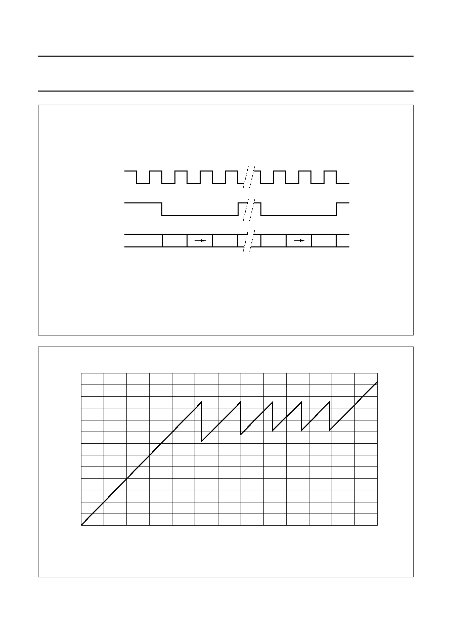
1996 Oct 29
44
Philips Semiconductors
Objective specification
GSM signal processing IC
PCF5083
Fig.15 Baseband RX Timing diagram.
handbook, full pagewidth
MGE294
SIXD
SIXEN
(2.27 kHz)
SIXCLK
(13 MHz)
I15
I0
Q15
Q0
Fig.16 AGC characteristic.
handbook, full pagewidth
0
-
20
-
40
-
60
-
80
-
100
-
120
absolute input level (dBm)
0
MGE295
-
10
-
20
-
30
-
40
-
50
-
60
ADC
output
(dB)
(1)

1996 Oct 29
45
Philips Semiconductors
Objective specification
GSM signal processing IC
PCF5083
9.1.2
GMSK M
ODULATOR
I
NTERFACE
The PCF5083 serial output port SOX is used to transmit
the coded, interleaved and formatted bits to the GMSK
modulator in the PCF5072 baseband interface IC.
The SOX port consists of:
·
Serial Output Data signal (SOXD)
·
Serial Output Clock signal (SOXCLK), running at
270.83 kHz
·
Serial Output Enable signal (SOXEN), active LOW.
The GSM bit clock is directly used as the external shift
clock, therefore no external buffering of transmission data
is necessary.
The PCF5083 general purpose I/O pin IO4 is used to
enable or disable the transmitter during DTX. If IO4 = 0,
the transmitter is enabled. If IO4 = 1, the transmitter is
disabled. It is sampled by the TDMA timer at the beginning
of the transmit burst period.
9.1.2.1
Burst format
Tables 29 and 30 show the format of the normal and
access burst produced by the DSP. The period of the
8 leading bits allows the power amplifier to ramp-down and
ramp-up.
Table 29 Normal burst format
BITS
NUMBER
OF BITS
DESCRIPTION
0 to 7
8
dummy bits (set to logic 1)
8 to 155
148
BN0 to BN147 in accordance
with
"GSM Rec. 05.02"
Table 30 Access burst format
9.1.3
A
UDIO AND
D
ATA
I
NTERFACE
The PCF5083 serial port Y is connected on-chip to the
IOM
®
-2 interface of the Timer Core. It is used for
connection to the following devices:
·
PCM codec in the PCF5072
·
Digital Audio Interface (DAI), used during type approval
·
Terminal adaptor for data services
·
External digital answering machine.
The physical transfer order on the IOM
®
-2 bus is 16-bit,
MSB first. The following signals are used:
·
Serial data input SIYD
·
Serial data output SOYD
·
Serial shift clock SIYCLK
·
Frame synchronization input SIYEN.
The DSP by default reads and writes the first 16-bit
timeslot of the IOM
®
-2 interface. This may be changed with
the appropriate software command to any 16-bit timeslot.
Input and output from/to the IOM
®
-2 bus is performed via
two FIFOs named audio input and audio output FIFO.
These FIFOs are implemented by firmware. Each FIFO is
able to store up to 297 16-bit samples.
BITS
NUMBER
OF BITS
DESCRIPTION
0 to 7
8
dummy bits (set to logic 1)
8 to 95
88
BN0 to BN87 in accordance
with
"GSM Rec. 05.02"
96 to 155
60
dummy bits (set to logic 1)
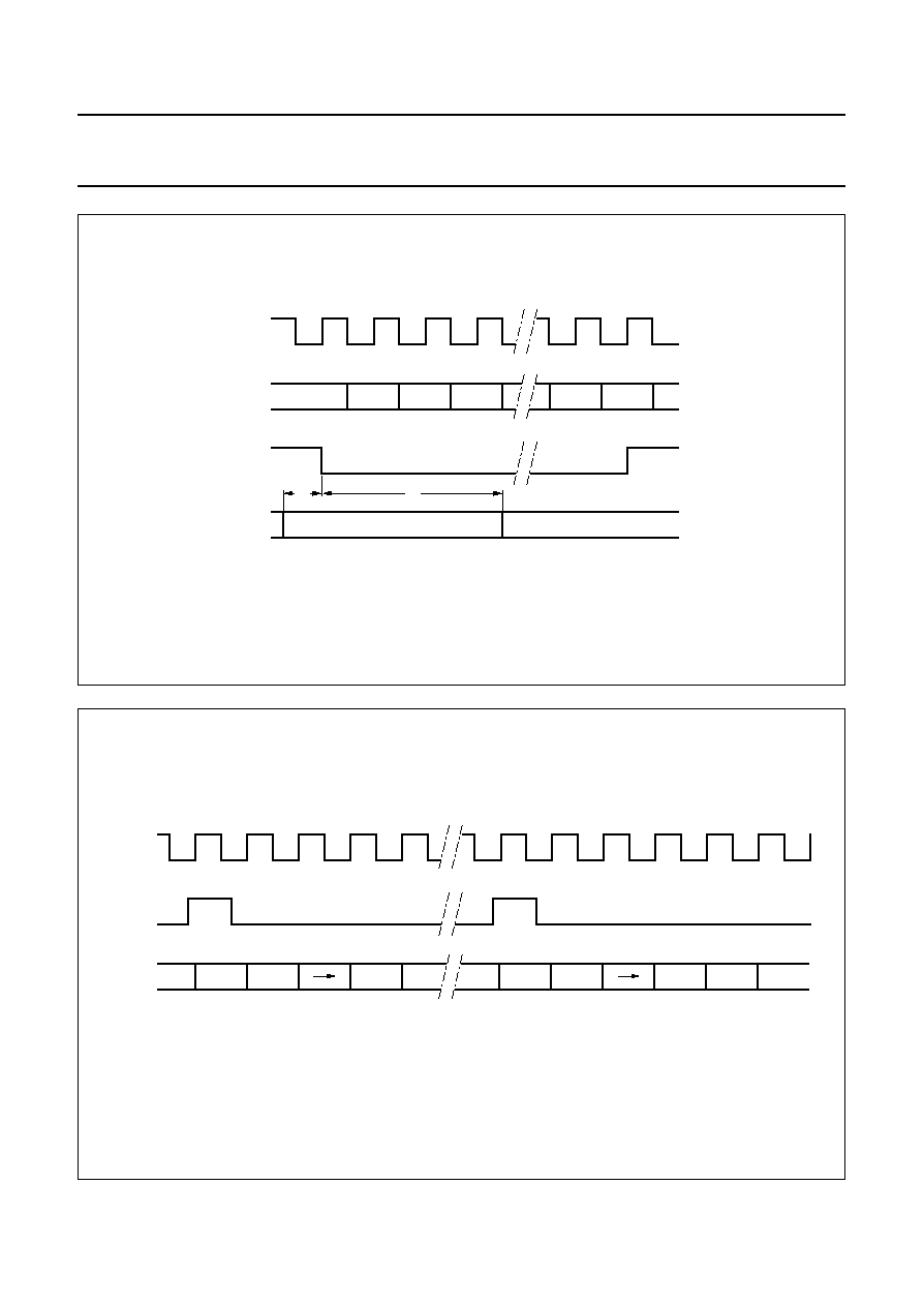
1996 Oct 29
46
Philips Semiconductors
Objective specification
GSM signal processing IC
PCF5083
Fig.17 GMSK modulator timing diagram.
handbook, full pagewidth
MGE296
IO4
(DTX)
SOXEN
SOXCLK
valid
tsu
th
b(0)
b(1)
b(2)
SOXD
b(154)
b(155)
DTX setup time: t
su
> 0
DTX hold time: t
h
> 124
×
3.69
µ
s
Fig.18 Audio and Interface timing (default).
handbook, full pagewidth
MGE297
B15
SIYD
SOYD
SIYEN
SIYCLK
B14
B0
1
1
B15
B14
B1
B0
1
1
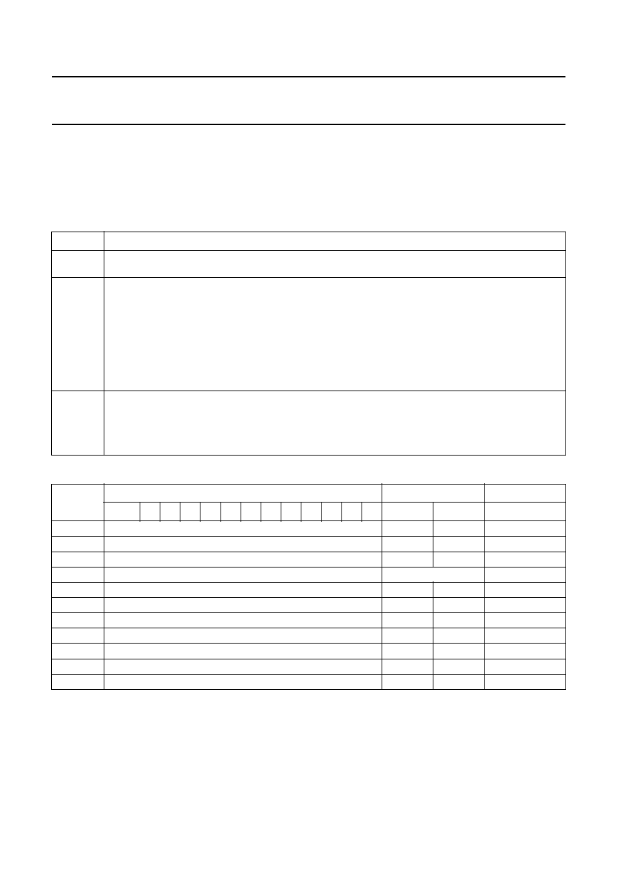
1996 Oct 29
47
Philips Semiconductors
Objective specification
GSM signal processing IC
PCF5083
9.1.4
A
UDIO INTERFACE
9.1.4.1
Downlink speech frame format
Every 20 ms the speech decoder in the DSP outputs a speech frame consisting of 160 16-bit words. These speech
frames are transmitted to the PCM codec. The speech frame format is described in Table 32.
Table 31 Field descriptions
Table 32 Downlink speech frame format
FIELD
DESCRIPTION
SAMPLE
This field contains the 13-bit linear PCM audio samples in two's complement (MSB = sign bit)
representation as defined by the
"GSM recommendation 06.01".
PARM
Whenever the speech decoder is active the PARM field is used to transfer the speech parameters
(D1 to D260) together with some frame classification information (see Table 99) and the currently
selected test mode (see Table 34) out of the DSP. The terms SP (speech flag), SID (silence descriptor)
and MUF (muting flag) are defined in
"GSM Rec. 06.31" (DTX for full-rate speech TCH). The HF bit
indicates, whether the speech codec is operating in handsfree mode (HF = 1) or not. The bits TM2 to TM0
are intended to be evaluated by an external Digital Audio Interface (DAI). They determine the currently
selected test mode during type approval as described in
"GSM Rec. 11.10, Section III.1.2.4.7".
TM2 to TM0 are passed in the TMODE file of the operation_mode parameter of the speech decoder
procedure. Refer to Section 9.3.1 for more information.
SYNC
Synchronization signal for external (test) equipment. Marks the 20 ms speech frames. Each falling edge
of SYNC marks the beginning of a new output speech frame and with a constant offset due to internal
module processing time the rising edge of SYNC marks a new input speech frame. As soon as audio
output data are available this bit always reflects the internal speech frame timing independently of other
processing tasks of the DSP.
OFFSET
SAMPLE FIELD
PARM FIELD
SYNC FIELD
15
14
13
12
11
10
9
8
7
6
5
4
3
2
1
0
0
audio sample 0
TM1
TM0
0
1
audio sample 1
HF
TM2
0
2
audio sample 2
0
0
.
3 to 27
audio samples 3 to 27
not used
.
28
audio sample 28
SID
0
0
29
audio sample 29
MUF
SP
.
30
audio sample 30
D2
D1
.
31
audio sample 31
D4
D3
.
32 to 157
audio samples 32 to 157
.
.
.
158
audio sample 158
D258
D257
.
159
audio sample 159
D260
D259
1

1996 Oct 29
48
Philips Semiconductors
Objective specification
GSM signal processing IC
PCF5083
Table 33 Frame classification
Table 34 Test mode selection
FRAME TYPE
SP
SID2
MUF
Speech frame
1
0
0
Transmitted SID
0
1
0
Repeated SID
0
0
0
Silence frame
1
0
1
Reserved
all other codes
DESCRIPTION
TM2
TM1
TM0
Normal operation (no tested divide via DAI)
0
0
0
Test of speech decoder/DTX functions (downlink)
0
0
1
Test of speech encoder/DTX functions (uplink)
0
1
0
Test of acoustic devices and ADCs and DACs
1
0
0
Reserved
all other codes
1996 Oct 29
49
Philips Semiconductors
Objective specification
GSM signal processing IC
PCF5083
9.1.4.2
Uplink Speech Frame Format
Every 20 ms the speech encoder in the DSP requires a speech frame consisting of 160 16-bit words. The speech frame
format is described in Table 36. Each word consists of three fields as shown in Table 35.
Table 35 Field descriptions
Table 36 Uplink speech frame format
FIELD
DESCRIPTION
SAMPLE
This field contains the 13-bit linear PCM audio samples in two's complement (MSB = sign bit)
representation as defined by the
"GSM recommendation 06.01".
PARM
If the bypass_flag in SP_encoder_TCHFS procedure (see Section 9.3.1) is set to 1, the speech encoder
is bypassed and the bits D1 to D260 are used as the coded speech frame. If bypass_flag is set to 2, the
speech encoder is only bypassed, if the control flag BM0 is set to 1 and BM1 is set to 0. The SP_R flag
indicates, either a speech frame (SP_R = 1) or a silence frame (SP_R = 0) is transmitted. Before the
external device could send meaningful information, it has to synchronize to the rising edge of the
SYNC bit (see Table 43).
RESD,
RESE
RESet Decoder, RESet Encoder. In test mode (see Section 9.3.1 speech coding procedures) these bits
behave as a reset signal for the speech decoder/encoder on a LOW-to-HIGH transition, RESD/RESE
must remain set for at least 40 ms.
OFFSET
SAMPLE FIELD
PARM FIELD
RESD FIELD
15
14
13
12
11
10
9
8
7
6
5
4
3
2
1
0
0
audio sample 0
RESE
not used
RESD
1
audio sample 1
not used
.
2 to 27
audio samples 2 to 27
.
28
audio sample 28
BM1
BM0
.
29
audio sample 29
-
SP_R
.
30
audio sample 30
D2
D1
.
31
audio sample 31
D4
D3
.
32 to 157
audio samples 32 to 157
.
.
.
158
audio sample 158
D258
D257
.
159
audio sample 159
D260
D259
RESD
1996 Oct 29
50
Philips Semiconductors
Objective specification
GSM signal processing IC
PCF5083
9.1.5
T
ERMINAL ADAPTOR INTERFACE FOR DATA SERVICES
9.1.5.1
General description
In Fig.19 the block diagram of the data service architecture
using the PCF5083 is shown. The GSM terminal is
connected to an external terminal adaptor via the IOM
®
-2
interface (serial port Y) of the PCF5083. Channel coding in
accordance with
"GSM recommendation 05.03" is done by
the DSP, rate adaptation and e.g. Hayes command
handling is done by the terminal adaptor.
There are two types of information that have to be
exchanged between the terminal adaptor and the GSM
terminal:
1. User data that has to be transmitted via the air
interface. This is the input and output of the channel
codec in the PCF5083
2. Control data which has to be exchanged between the
System Controller and the terminal adaptor.
Data transfer via the IOM
®
-2 is done in form of data
frames. Each data frame contains 160 16-bit samples
(20 ms) and consists of a user data block containing user
data to/from the channel codec and a control data block
containing control data to/from the System Controller. The
DSP firmware (the procedures MP_read_data_frame and
MP_write_data_frame, see Section 9.3.1) performs
multiplexing and demultiplexing of user and control data.
Control data is forwarded to the System Controller or to the
terminal adaptor, respectively without modification or
interpretation by the DSP.
A fully integrated solution for the architecture of GSM data
services is in preparation, at which rate adaptation is
realised as an additional DSP software module, Hayes
command interpretation is part of the P90CL301 software
and data communications are done via the RS-232 port of
the P90CL301.
Fig.19 Block diagram of the GSM Data Services with the PCF5083.
handbook, full pagewidth
MGE317
TERMINAL
ADAPTOR
MUX
DEMUX
CHANNEL
CODEC
PCF5083
GSM TERMINAL
P90CL301
PCF5083 DEVICE DRIVER
LAYER 1, 2, 3, MMI, . . .
control data
user data
IOM-2
user &
control data
1996 Oct 29
51
Philips Semiconductors
Objective specification
GSM signal processing IC
PCF5083
9.1.5.2
Format of downlink data frames
The downlink data frame format is described in Table 40. Each word consists of four fields; these are described in
Table 37.
Table 37 Field descriptions
Table 38 Classification of the 16-bit samples
Table 39 Valid values for FID
Note
1. Binary value; X = don't care.
FIELD
DESCRIPTION
DATA
Depending on the contents of the CMD field (see Table 38), this field contains a data byte belonging to a
user or a control data block or auxiliary control information for the terminal adaptor.
CMD
This field classifies the 16-bit samples as described in the Table 38.
SYNC
Synchronization signal for external (test) equipment. Marks the 20 ms speech frames. Each falling edge of
SYNC marks the beginning of a new output speech frame and with a constant offset due to internal
module processing time the rising edge of SYNC marks a new input speech frame. As soon as audio
output data are available this bit always reflects the internal speech frame timing independently of other
processing tasks of the DSP.
INFO
This field may be used by external devices to distinguish between audio and data frames. The INFO field
of word#2 contains the so called frame identification (FID); see Table 39.
CMD FIELD
DESCRIPTION
7
6
5
4
3
0
0
0
0
1
The data field contains a valid data byte belonging to either a user or a control data block.
0
0
0
1
0
The data field contains auxiliary control information that may be used by the terminal
adaptor for synchronization purposes.
1
1
1
1
1
Indicates that the data field contains invalid data, which should be ignored.
Other combinations
Reserved for future expansion. Not used by the DSP.
FID
(1)
FRAME TYPE
00
audio frame
01
data frame
1X
reserved
1996 Oct 29
52
Philips Semiconductors
Objective specification
GSM signal processing IC
PCF5083
Table 40 Downlink data frame format
OFFSET
DATA FIELD
CMD FIELD
INFO FIELD SYNC FIELD
DESCRIPTION
15 14 13 12 11 10
9
8
7
6
5
4
3
2
1
0
0
0XFF
1
1
1
1
1
0
1
0
Header: to be
used by the
terminal adaptor
for
synchronization
purposes
1
0XFF
1
1
1
1
1
0
1
0
2
0XFF
1
1
1
1
1
FID = 01
0
3 to 21
0XFF
1
1
1
1
1
0
1
0
22
0X01
0
0
0
1
0
0
1
0
23
0XFF
1
1
1
1
1
0
1
0
24
0XFF
1
1
1
1
1
0
1
0
25
0X00
0
0
0
1
0
0
1
0
26
0XFF
1
1
1
1
1
1
1
1
User data block.
LU is the block
length.
Valid range:
0
LU
36.
27
0XFF
1
1
1
1
1
1
1
1
28
0XFF
1
1
1
1
1
1
1
1
29
LU
0
0
0
0
1
0
0
1
30
0XFF
1
1
1
1
1
1
1
1
0XFF
1
1
1
1
1
1
1
1
U[1]
0
0
0
0
1
1
1
1
0XFF
1
1
1
1
1
1
1
1
0XFF
1
1
1
1
1
1
1
1
U[2]
0
0
0
0
1
0
0
1
0XFF
1
1
1
1
1
1
1
1
U(LU
-
1)
0
0
0
0
1
0
0
1
0XFF
1
1
1
1
1
1
1
1
0XFF
1
1
1
1
1
1
1
1
U(LU)
0
0
0
0
1
0
0
1
0XFF
1
1
1
1
1
1
1
1
0XFF
1
1
1
1
1
1
1
1
LC
0
0
0
0
1
0
0
1
Control data
block; LC is the
block length.
Valid range:
0
LC
8.
0XFF
1
1
1
1
1
1
1
1
0XFF
1
1
1
1
1
1
1
1
C[0]
0
0
0
0
1
0
0
1
0XFF
1
1
1
1
1
1
1
1
0XFF
1
1
1
1
1
1
1
1
C[1]
0
0
0
0
1
0
0
1
0XFF
1
1
1
1
1
1
1
1
C(LC
-
2)
0
0
0
0
1
0
0
1
0XFF
1
1
1
1
1
1
1
1
0XFF
1
1
1
1
1
1
1
1
C(LC
-
1)
0
0
0
0
1
0
0
1
159
0XFF
1
1
1
1
1
1
1
1
1996 Oct 29
53
Philips Semiconductors
Objective specification
GSM signal processing IC
PCF5083
9.1.5.3
Format of uplink data frames
The uplink data frame format is described in Table 43. Each word consists of four fields; these are described in Table 41.
Table 41 Field descriptions
Table 42 Classification of the 16-bit samples
Note
1. The external terminal adaptor may insert at any position an arbitrary number of fill words with CMD = 11111.
Table 43 Uplink data frame format
Notes
1. X = don't care.
FIELD
DESCRIPTION
DATA
This field contains the data bytes of user data block and control data block. Only words with
CMD = 00001 contain valid data fields (see Table 42).
CMD
This field classifies the 16-bit samples as described in the Table 42.
SYNC, INFO
In uplink direction, these fields are without meaning.
CMD FIELD
DESCRIPTION
7
6
5
4
3
0
0
0
0
1
The data field contains a valid data byte belonging to either a user or a control data block.
0
0
0
1
0
The data field contains auxiliary control information that may be used by the terminal
adaptor for synchronization purposes; note 1.
1
1
1
1
1
Indicates that the data field contains invalid data, which should be ignored.
Other combinations
Reserved for future expansion. Not used by the DSP.
OFFSET
DATA FIELD
(1)
CMD FIELD
INFO FIELD
SYNC
FIELD
DESCRIPTION
15 14 13 12 11 10
9
8
7
6
5
4
3
2
1
0
0
X
1
1
1
1
1
X
X
X
User data block; this block
contains modified CCITT
frame in accordance with
"GSM Rec. 05.03". It is
used as input data for the
channel encoder. LU is the
block length
Valid range: 0
LU
33
X
1
1
1
1
1
X
X
X
LU
0
0
0
0
1
X
X
X
U[0]
0
0
0
0
1
X
X
X
U[1]
0
0
0
0
1
X
X
X
U(LU
-
2)
0
0
0
0
1
X
X
X
U(LU
-
1)
0
0
0
0
1
X
X
X
LC
0
0
0
0
1
X
X
X
Control data block; the
first byte LC is the block
length. LC may also be
zero. This block is
forwarded to the System
Controller.
Valid range: 0
LC
10.
C[0]
0
0
0
0
1
X
X
X
C[1]
0
0
0
0
1
X
X
X
C(LC
-
2)
0
0
0
0
1
X
X
X
C(LC
-
1)
0
0
0
0
1
X
X
X
159
X
1
1
1
1
1
X
X
X
1996 Oct 29
54
Philips Semiconductors
Objective specification
GSM signal processing IC
PCF5083
9.1.5.4
User data block formats
In the following sections the user data block formats for all
data channels defined in
"GSM Rec. 05.03" are explained.
The formats for uplink and downlink directions are identical
with the exception that three additional bytes are
transmitted in the downlink direction:
·
The first byte contains the facch_flag. This flag indicates
whether the channel decoder has decoded a FACCH
(facch_flag = 1) or not (facch_flag = 0).
·
The other two bytes, rxqual_ber_low and
rxqual_ber_high, indicate the estimated Bit Error Rate
(BER) at the channel decoder input.
The Bit Error Rate can be calculated using the following
equation:
Tables 44 to 47 show the user data block format for
full-rate and half-rate data channels running at different
baud rates.
Note that the TCH/H4.8 format is used for half-rate data
channels at 4.8 kbits/s. It is equivalent to the format used
for TCH/F9.6 (see Table 46).
BER
rxqual_ber_low
256
rxqual_ber_high
×
+
4096
----------------------------------------------------------------------------------------------------------
=
Table 44 TCH/F2.4
The following table shows the user data block for full rate data channel at 2.4 kbit/s (and less). The 2
×
36 data bits
shown correspond to 2 modified CCITT V.110 36-bit frames.
DESCRIPTION
OFFSET
DOWNLINK DATA
UPLINK DATA
Block size
0
14
11
Valid flag
1
1
1
Modified CCITT frame 1
2
rb8 to rb1
rb8 to rb1
3
rb16 to rb9
rb16 to rb9
4
rb24 to rb17
rb24 to rb17
5
rb32 to rb25
rb32 to rb25
6
rb36 to rb33
rb36 to rb33
Modified CCITT frame 2
7
rb8 to rb1
rb8 to rb1
8
rb16 to rb9
rb16 to rb9
9
rb24 to rb17
rb24 to rb17
10
rb32 to rb25
rb32 to rb25
11
rb36 to rb33
rb36 to rb33
FACCH flag
12
facch_flag
-
rxqual_ber
13
rxqual_ber_low
-
14
rxqual_ber_high
-

1996 Oct 29
55
Philips Semiconductors
Objective specification
GSM signal processing IC
PCF5083
Table 45 TCH/F4.8
The following table shows the user block data format for full rate data channel at 4.8 kbit/s. The 2
×
60 data bits shown
correspond to 2 modified CCITT V.110 60-bit frames according to
"GSM 04 21".
DESCRIPTION
OFFSET
DOWNLINK DATA
UPLINK DATA
Block size
0
20
17
Valid flag
1
1
1
Modified CCITT frame 1
2
rb8 to rb1
rb8 to rb1
3
rb16 to rb9
rb16 to rb9
4
rb24 to rb17
rb24 to rb17
5
rb32 to rb25
rb32 to rb25
6
rb40 to rb33
rb40 to rb33
7
rb48 to rb41
rb48 to rb41
8
rb56 to rb49
rb56 to rb49
9
rb60 to rb57
rb60 to rb57
Modified CCITT frame 2
10
rb8 to rb1
rb8 to rb1
11
rb16 to rb9
rb16 to rb9
12
rb24 to rb17
rb24 to rb17
13
rb32 to rb25
rb32 to rb25
14
rb40 to rb33
rb40 to rb33
15
rb48 to rb41
rb48 to rb41
16
rb56 to rb49
rb56 to rb49
17
rb60 to rb57
rb60 to rb57
FACCH flag
18
facch_flag
-
rxqual_ber
19
rxqual_ber_low
-
20
rxqual_ber_high
-

1996 Oct 29
56
Philips Semiconductors
Objective specification
GSM signal processing IC
PCF5083
Table 46 TCH/F9.6
The following table shows the full rate data channel at 9.6 kbit/s. The 4
×
60 data bits shown correspond to
4 modified CCITT V.110 60-bit frames in accordance with
"GSM 04.21". For non-transparent services those four blocks
shall align with one 240-bit RLP frame. The valid_flag indicates, whether the data block contains valid data
(valid_flag = 1) or not (valid_flag = 0). It is used for DTX.
DESCRIPTION
OFFSET
DOWNLINK DATA
UPLINK DATA
Block size
0
36
33
Valid flag; note
1
1
valid flag
Modified CCITT frame 1
2
rb8 to rb1
rb8 to rb1
3
rb16 to rb9
rb16 to rb9
4
rb24 to rb17
rb24 to rb17
5
rb32 to rb25
rb32 to rb25
6
rb40 to rb33
rb40 to rb33
7
rb48 to rb41
rb48 to rb41
8
rb56 to rb49
rb56 to rb49
9
rb60 to rb57
rb60 to rb57
Modified CCITT frame 2
10
rb8 to rb1
rb8 to rb1
11
rb16 to rb9
rb16 to rb9
12
rb24 to rb17
rb24 to rb17
13
rb32 to rb25
rb32 to rb25
14
rb40 to rb33
rb40 to rb33
15
rb48 to rb41
rb48 to rb41
16
rb56 to rb49
rb56 to rb49
17
rb60 to rb57
rb60 to rb57
Modified CCITT frame 3
18
rb8 to rb1
rb8 to rb1
19
rb16 to rb9
rb16 to rb9
20
rb24 to rb17
rb24 to rb17
21
rb32 to rb25
rb32 to rb25
22
rb40 to rb33
rb40 to rb33
23
rb48 to rb41
rb48 to rb41
24
rb56 to rb49
rb56 to rb49
25
rb60 to rb57
rb60 to rb57
Modified CCITT frame 4
26
rb8 to rb1
rb8 to rb1
27
rb16 to rb9
rb16 to rb9
28
rb24 to rb17
rb24 to rb17
29
rb32 to rb25
rb32 to rb25
30
rb40 to rb33
rb40 to rb33
31
rb48 to rb41
rb48 to rb41
32
rb56 to rb49
rb56 to rb49
33
rb60 to rb57
rb60 to rb57
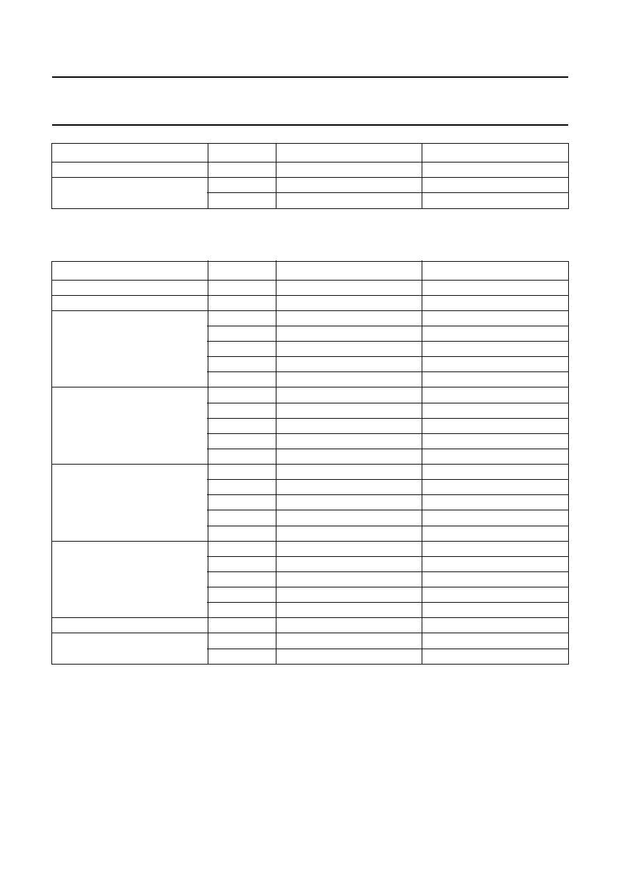
1996 Oct 29
57
Philips Semiconductors
Objective specification
GSM signal processing IC
PCF5083
Table 47 TCH/H2.4
The following table shows the user data block for half rate data channel at 2.4 kbit/s (and less). The 4
×
36 data bits
shown correspond to 4 modified CCITT V.110 36-bit frames according to GSM 04 21.
FACCH flag
34
facch_flag
-
Rxqual_ber
35
rxqual_ber_low
-
36
rxqual_ber_high
-
DESCRIPTION
OFFSET
DOWNLINK DATA
UPLINK DATA
Block size
0
24
21
Valid flag
1
1
1
Modified CCITT frame 1
2
rb8 to rb1
rb8 to rb1
3
rb16 to rb9
rb16 to rb9
4
rb24 to rb17
rb24 to rb17
5
rb32 to rb25
rb32 to rb25
6
rb36 to rb33
rb36 to rb33
Modified CCITT frame 2
7
rb8 to rb1
rb8 to rb1
8
rb16 to rb9
rb16 to rb9
9
rb24 to rb17
rb24 to rb17
10
rb32 to rb25
rb32 to rb25
11
rb36 to rb33
rb36 to rb33
Modified CCITT frame 3
12
rb8 to rb1
rb8 to rb1
13
rb16 to rb9
rb16 to rb9
14
rb24 to rb17
rb24 to rb17
15
rb32 to rb25
rb32 to rb25
16
rb36 to rb33
rb36 to rb33
Modified CCITT frame 4
17
rb8 to rb1
rb8 to rb1
18
rb16 to rb9
rb16 to rb9
19
rb24 to rb17
rb24 to rb17
20
rb32 to rb25
rb32 to rb25
21
rb36 to rb33
rb36 to rb33
FACCH flag
22
facch_flag
-
Rxqual_ber
23
rxqual_ber_low
-
24
rxqual_ber_high
-
DESCRIPTION
OFFSET
DOWNLINK DATA
UPLINK DATA
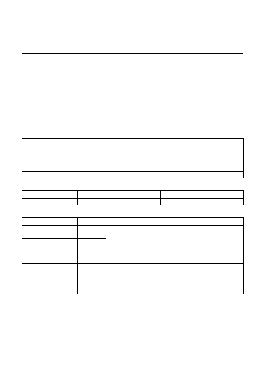
1996 Oct 29
58
Philips Semiconductors
Objective specification
GSM signal processing IC
PCF5083
9.1.6
S
YSTEM
C
ONTROLLER INTERFACE
The PCF5083 parallel port is used for communication with the P90CL301 System Controller (SC) which is compatible
with the 68000 family microcontrollers. Details about interfacing are described in Chapter 10.
The host port of the DSP has three internal registers:
1. PI; 16-bit parallel input register (write-only)
2. PO; 16-bit parallel output register (read-only)
3. PIOS; 5-bit parallel I/O Status/Control register (see Table 50).
The 16-bit words of registers PI and PO are transferred in two access cycles of 8-bits. The LOW byte/HIGH byte selection
is controlled with HA0 and with bit 5 of the PIOS register, PLSB. For correct interrupt generation the transfer order should
be HA1 and HA0 = 00; then HA1 and HA0 = 01 (see Table 48).
Table 48 Host port register addressing
Table 49 Status/Control Register (PIOS)
Table 50 Description of PIOS bits
PLSB
HA1
HA0
DESCRIPTION
STATUS REGISTER PIOS
CHANGE
0 (1)
0
0
access PI/PO HIGH (LOW) byte
no change
0 (1)
0
1
access PI/PO LOW (HIGH) byte
PISE = 0 or POSF = 0
X
1
0
reserved
no change
X
1
1
read status register PIOS
no change
7
6
5
4
3
2
1
0
-
-
-
PLSB
PORQEN
PIRQEN
POSF
PISE
BIT
NAME
DIRECTION
DESCRIPTION
7
-
-
These three bits are not used.
6
-
-
5
-
-
4
PLSB
read
This bit controls the parallel transfer order. When PLSB = 1; the LSB is
transferred first. The reset value is a logic 1.
3
PORQEN
read/write
When PORQEN = 1; PORQN is enabled. The reset value is a logic 0.
2
PIRQEN
read/write
When PIRQEN = 1; PIRQN is enabled. The reset value is a logic 0.
1
POSF
read
When POSF = 1; the Output Register (PO) is full. The reset value is a
logic 0.
0
PISE
read
When PISE = 1; the Input Register (PI) is empty. The reset value is a
logic 1.

1996 Oct 29
59
Philips Semiconductors
Objective specification
GSM signal processing IC
PCF5083
The host can be used in three modes:
1. Acknowledge mode: in this mode the PCF5083
provides an open drain output DTACK, that
acknowledges data read or write accesses to the host
port registers PI, PO or PIOS. This signal has to be
connected to the 90CL301 DTACK input. Using the
hardware handshake via DTACK, the 90CL301 can
write data to the PI register at any time. It is not
necessary to poll the PISE bit in the status register
PIOS. If the 90CL301 writes to PI and PI is still full, the
write access is automatically extended until the DSP
has read PI. Under worst case conditions this will last
10
µ
s (see formula below). Before reading a message
via PO however, the System Controller has to check
once if a message is available from DSP. This is done
by polling the POSE flag in the PIOS register. If POSE
is a logic 1 the System Controller has to read the first
word of the message. After determination of the
message length, the rest of the message can be read
without further polling.
2. Polling mode: in this mode the hardware handshake
via DTACK is not used. Before writing a word to PI, the
90CL301 must wait until the PISE flag in the Status
Register PIOS is set. Correspondingly, the 90CL301
must wait until the POSE flag in PIOS is set, before
reading PO.
3. Interrupt mode: in this mode the PCF5083 provides
two internal interrupt request signals PIRQN and
PORQN. Signal PIRQN (active LOW) corresponds to
status register bit PISE (active HIGH) and PORQN
(active LOW) to bit POSF (active HIGH). As soon as
the status bit PISE or POSF is set, PIRQN/PORQN is
going LOW, generating an interrupt at the host. The
interrupt service routines should handle the two 8-bit
transfers. After the first transfer PIRQN/PORQN goes
HIGH, removing the interrupt source. After the second
transfer a new interrupt will be generated.
PIRQN and PORQN can be enabled by setting PIOS
bit 2 for PIRQ_EN and bit 3 for PIRQ_EN to HIGH.
After reset both signals are disabled. The PIRQN and
PORQN interrupt condition is signalled via the
HIPR_INT interrupt line (see Section 10.2).
Command and indication messages are buffered in
two queues, each of 139 words. If working in acknowledge
mode the layer 1 software in the 90CL301 has to ensure
that no queue overflow occurs (this will never happen
during normal operation).
The times TPI and TPO required by the DSP to receive or
transmit a message consisting of N words can be
calculated according to the following formulas:
TPI = 10
µ
s + (N
-
1)
×
1.5
µ
s
TPO = N
×
1.5
µ
s
Data transfer in acknowledge mode produces the least
overhead in the 90CL301 layer 1 software. It is therefore
recommended to use the acknowledge mode for
communication with the DSP.
9.1.7
E
VENT
C
OUNTER
C
LOCK
The event counter is used by the firmware for time-out
detection.The 32.768 kHz clock is internally connected to
the ECLK input of the DSP.
9.1.8
G
ENERAL
P
URPOSE
I/O P
INS
Table 51 Usage of General Purpose I/O Pins
Note that the IO1 pin is not changed automatically by the
DSP firmware (e.g. by the procedure MP_iom2_enable).
Whenever audio data should be transmitted via the audio
interface, IO1 has to be set explicitly by calling the
procedure DB_write_register:
DB_write_register(11, 0x0100, 1) sets the IO1 bit in
register SIOC
DB_write_register(11, 0x0100, 2) resets the IO1 bit in
register SIOC.
PIN
RESET
DEFAULT
DESCRIPTION
IO1
0
Audio interface of the timer core
select pin. A logic 1 enables the
interface; a logic 0 disables the
interface.
IO2
1
used for procedure trace
IO3
1
used for procedure trace
IO4
1
DTX select pin. A logic 1 enables
the transmitter; a logic 0 disables
the transmitter.

1996 Oct 29
60
Philips Semiconductors
Objective specification
GSM signal processing IC
PCF5083
9.1.9
P
OWER SAVING MODES
9.1.9.1
Idle mode
When operating in Idle mode the DSP enters a dormant
state and requires only a fraction of the power normally
needed to supply the device in the full operating mode.
The processor core is switched off whereas the I/O section
of the processor is fully functional. The Idle mode is
invoked by the on-chip firmware whenever the DSP is
waiting for an I/O event. The DSP automatically leaves the
Idle mode as soon as the input or output operation has
been completed.
9.1.9.2
Power-down mode
The Power-down mode is initiated when the signal
DSPON is deactivated during Sleep mode (see
Section 8.3.3). The DSP will stop operation synchronously
after a maximum of 3 CLKI cycles delay. All parts of the
DSP which operate with the main processor clock are in
static state. Only the blocks running with the serial
interface clocks are not affected by the Power-down mode.
For minimum power consumption the external serial shift
clocks should therefore be switched off. The DSP remains
in the power-down state as long as the signal DSPON is
held inactive. The processor continues its operation for a
maximum of 3 clock cycles after the signal DSPON is set
active again.
9.2
Message Interface to the System Controller
The DSP can be controlled with commands and joining
16-bits parameters from the System Controller via the host
port register PI. The first word always contains the
command OPCODE and length. The second word is an
arbitrary ID code which is useful for debugging purposes.
The following words are command parameters. The DSP
can also generate indications giving status information or
requested data. These indication messages can be read
(R) via host port register PO.
The DMA message is used to download data into the
program/data RAM. Download is always done into the
data address space. The parameters mc_before and
mc_after indicate the value of the Memory Configuration
Register before and after download. Thus, it is possible to
switch a RAM bank into the data address space, download
a program and switch it back afterwards. For more
information about the MC Register and the PCF5083
memory mapping please refer to
"Information Manual
Digital Signal Processors PCF508x, Philips
Semiconductors, 1995".
Table 52 Commands/indications to/from the PCF5083
Note
1. X = don't care.
MNEMONIC
DIRECTION
OPCODE
(1)
bit 15 to bit 8
LENGTH
bit 7 to bit 0
ID
DATA
DMA
write
0X0000
msg_id
mc_before n_words;
address data [1] to data [n words];
mc_after
EXEC_PROC
write
0X01
3 + npar
msg_id
proc_id;
parameter_1 to parameter_N
PROC_RETUR
N
read
0X11
3 + n_retvals
msg_id
proc_id;
return_value 1 to return value_N
PACKET
write
0X02
2 + N (cmd_len)
msg_id
cmd_1 to cmd_N
RESET
write
0X03
3
msg_id
reset_parm
NOP
write
0X05
2 + N
msg_id
data_1 to data_N
ERROR
read
0X12
3
msg_id
error_code

1996 Oct 29
61
Philips Semiconductors
Objective specification
GSM signal processing IC
PCF5083
9.2.1
E
XECUTION OF
GSM
BASEBAND PROCEDURES
The EXEC_PROC commands initiate the execution of
internal procedures. The procedure specified by proc_id is
executed within the DSP. The input parameters of the
procedure are part of the message. The return values (if
any) of the procedure and the msg_id parameter are
packed to a PROC_RETURN indication.
Several commands can be combined with the PACKET
command to reduce overhead especially when sending
commands to the DSP in polling mode.
9.2.2
N
O
O
PERATION
(NOP)
COMMAND
This NOP command may be used for debugging
purposes. It is ignored by the DSP. The length of the data
field has to be at least one word.
9.2.3
S
OFT RESETTING THE
DSP
The RESET command causes the DSP to perform a soft
reset. It is executed immediately after the current running
procedure is completed. Depending on the reset
parameter (see Table 53) the input and/or output
command queues are cleared. It is possible to reset more
than one FIFO or queue, by setting the appropriate bits.
Table 53 Parameter of RESET message
Note
1. X = don't care.
MNEMONIC
VALUE
(1)
DESCRIPTION
RESET_ALL
0X0000
Restart main program (soft reset), clear all buffers and queues and
all external memory.
OUTPUT_MESSAGE_QUEUE
0X0001
Clear the output message queue.
INPUT_MESSAGE_QUEUE
0X0002
Clear the input message queue.
BBD_IN_FIFO
0X0004
Clear the baseband digitizer input FIFO.
MOD_OUT_FIFO
0X0008
Clear the GMSK modulator output FIFO.

1996 Oct 29
62
Philips Semiconductors
Objective specification
GSM signal processing IC
PCF5083
9.2.4
E
RROR HANDLING
The ERROR indication notifies the SC that an error has occurred in previously submitted EXEC PROC commands with
ID msg_id. Table 54 shows all possible error codes. After the detection of an error, the current command is aborted and
the DSP continues execution of the next command in the input queue.
Table 54 Error codes
Note
1. These error codes do not notify a real error; they indicate the occurrence of a special event.
MNEMONIC
CODE
DESCRIPTION
RESET_OCCURRED
1
the DSP main program restarted
MSG_TYP_UNKNOWN
5
an undefined command was received by the DSP
WRONG_PARAMETER
10
one of the procedure parameters is not in a valid range
MSG_IN_FIFO_OVERFLOW
11
an input queue overflow occurred
MSG_OUT_FIFO_OVERFLOW
12
an output queue overflow occurred
BBD_IN_FIFO_OVERFLOW
13
a BBD FIFO overflow occurred
MOD_FIFO_FULL
14
the modulator FIFO is not empty enough to receive all data
AUDIO_IN_IFO_OVERFLOW
15
an audio input FIFO overflow occurred
AUDIO_OUT_FIFO_UNDERFLOW
16
an audio output FIFO underflow occurred
AUDIO_OUT_FIFO_FULL
17
the audio output FIFO is not empty enough to receive all data
TIMEOUT_BBD_IN_FIFO
20
a time-out occurred waiting for BBD samples
TIMEOUT_AUDIO_IN_FIFO
21
a timeout occurred waiting for audio input samples
AUDIO_SYNC_FAILED
22
the audio synchronization was not successful
AUDIO_SYNC_TIMEOUT
26
MP_audio_sync waited too long for the first BBD sample
FSC_TIMEOUT
27
MP_iom2_enable waited too long for the frame sync interrupt
AUDIO_SAMPLES_INSERTED
28
(1)
MP_audio_sync inserted audio samples into the audio FIFO
AUDIO_SAMPLES_REMOVED
29
(1)
MP_audio_sync removed audio samples from the audio FIFO
SPEECH_ENCODER_RESET
31
(1)
a speech encoder reset occurred
SPEECH_DECODER_RESET
32
(1)
a speech decoder reset occurred

1996 Oct 29
63
Philips Semiconductors
Objective specification
GSM signal processing IC
PCF5083
9.3
GSM baseband procedures
The baseband procedures with optional input parameters can be called by the EXEC_PROC command as described in
Section 9.2. Return values are packed in the PROC_RETURN indication. Every procedure deals with the following types
of data:
·
Input parameters which are directly supplied by the System Controller
·
Return values which are automatically sent to the System Controller as soon as the procedure is completed
·
Input and output data buffers located in the DSP data RAM. They are used for communication with other procedures.
Most of the procedures use a common buffer SCRATCH_BUFF for their input and output data. Only a small number
of procedures need specific buffer for input or output. In this case there are one or two additional parameters in_buff_id
or out_buff_id which determine the buffers where input and output data are located. In Table 55 a list of all available
buffers is given.
For all trailing parameters of a procedure which are not transmitted with the EXEC_PROC command a default value of
zero is used.
Table 55 Data buffers for baseband procedures
Notes
1. X = don't care.
MNEMONIC
ID
(1)
SIZE
DESCRIPTION
VERSION_BUFF
0X8000
10
Contains the BCD coded version numbers of all software packages (order:
MP, BB, CI, CM, DB, EM, FB, SP and TP). A version number 0Xmm.ss
means version mm.ss.
SCRATCH_BUFF
0X8001
167
Scratch buffer for communication between arbitrary modules.
TCH_CMI_BUFF
0X8002
116
The combination of the 4 buffers; TCH_CMI_BUFF1 to TCH_CMI_BUFF4.
TCH_CMI_BUFF1
0X8003
29
Used to store the CMI values of 4 consecutive bursts belonging to one TCH
block.
TCH_CMI_BUFF2
0X8004
29
TCH_CMI_BUFF3
0X8005
29
TCH_CMI_BUFF4
0X8006
29
CCH_CMI_BUFF
0X8007
116
The combination of the 4 buffers; CCH_CMI_BUFF1 to CCH_CMI_BUFF4.
CCH_CMI_BUFF1
0X8008
29
Used to store the CMI values of 4 consecutive bursts belonging to one
CCH block.
CCH_CMI_BUFF2
0X8009
29
CCH_CMI_BUFF3
0X800A
29
CCH_CMI_BUFF4
0X800B
29
CCH_INFO_BUFF
0X800C
32
The combination of the 4 buffers;
CCH_INFO_BUFF1 to CCH_INFO_BUFF4.
CCH_INFO_BUFF1
0X800D
8
Used to store the information bits 4 bursts belonging to one CCH block.
CCH_INFO_BUFF2
0X800E
8
CCH_INFO_BUFF3
0X800F
8
CCH_INFO_BUFF4
0X8010
8
TCH_LOOP_BUFF
0X8011
82
Used to store four normal bursts during TCH loop-back operation. Note this
buffer is also used by the speech encoder.
MP_CONTROL_BUFF
0X8013
6
Used to control several features of the firmware; see Table 56.
IQ_BUFF
0X8018
334
Used to store I and Q components from the PCF5072. This buffer is
overlaid with SCRATCH_BUFF.

1996 Oct 29
64
Philips Semiconductors
Objective specification
GSM signal processing IC
PCF5083
The MP_CONTROL_BUFF may be used to control several features of the DSP. It consists of 4 parameter fields as given
in Tables 56 and 57.
Table 56 Contents of MP_CONTROL_BUFF
Table 57 Associated I/O pins
Note
1. If proc_trace_buff[1] is 0, then IO3 is set on errors.
OFFSET
DESCRIPTION
0
time-out_freq: ECLK input frequency divided by 10 kHz. After reset time-out_freq is set to
3 (32.768 kHz clock).
1
eclk_cycle_count: contains number of ECLK cycles spent most recently called procedure. Required for
test purposes only.
2 to 4
proc_trace_buff[2]: for debugging purposes the DSP provides a procedure trace facility. The IDs of the
procedures to be traced must be stored in proc_trace_buff. If any of these procedures is executing, its
corresponding I/O pin (see Table 57) is set to a logic 0.
LOCATION
I/O PIN
DEFAULT AFTER RESET
proc_trace_buff[0]
IO2
17 CP_rx_normal_burst
proc_trace_buff[1]
IO3
00 trace errors; note 1

1996 Oct 29
65
Philips Semiconductors
Objective specification
GSM signal processing IC
PCF5083
9.3.1
P
ROCEDURE DESCRIPTION
In this section all baseband procedures offered by the DSP are listed in alphabetical order. The following naming
conventions are used throughout the description:
·
Value: this is a 16-bit integer parameter (call by value) or return value (e.g. training sequence code, dtx flag)
·
Value [SIZE]: this is an array consisting of SIZE 16-bit words. The array is transmitted word by word between the
System Controller and the DSP (e.g. FACCH msg[12])
·
Parameter names ending with buff_id identify a buffer in the DSP data RAM where input or output data of the
procedure is stored.
Table 58 Procedure description
DESCRIPTION
ID
PARAMETERS
RETURN
VALUES
BB_access_burst
Burst building of a random access burst in accordance with
"
GSM Rec. 05.02". The burst information bits must be located in
SCRATCH_BUFF. The result is returned in SCRATCH_BUFF.
1
-
-
BB_normal_burst
Burst building of n_bursts normal bursts in accordance with
"GSM Rec. 05.02". The burst information bits must be located in the buffer
determined by info_buff_id. The result is returned in buffer burst_buff_id.
`tsc' is the training sequence code (range: 0 to 7)
2
info_buff_id
burst_buff_id
tsc
n_bursts
-
CI_decrypt (note 1)
Decryption of the CMI values of n_bursts bursts stored in buffer
cmi_buff_id.
Note that n_bursts may be in the range from 1 to 4. If n_bursts is set to 4,
cmi_buff_id must not be any other than TCH_CMI_BUFF or
CCH_CMI_BUFF
3
cmi_buff_id
n_bursts
-

1996 Oct 29
66
Philips Semiconductors
Objective specification
GSM signal processing IC
PCF5083
CI_decrypt_init (note 1)
Initialization for CI_decrypt. The decrypt_flag enables or disables
decryption.
decrypt_flag = 0, means no decryption.
decrypt_flag = 1, decryption according to A5/1.
decrypt_flag = 2, decryption according to A5/2
t1 is absolute Frame Number (FN) divisor 26
×
51 (0 to 2047,11 bits).
t2 is absolute Frame Number (FN) modulo 26 (0 to 25, 5 bits)
t3 is absolute Frame Number (FN) modulo 51 (0 to 50, 6 bits)
key[0 to 3] contains 64 bits of the ciphering key K
c
in accordance with
"GSM Rec. 03.20". The bits are loaded by the algorithm in LSB first order
(first bit = LSB {key[0]}, last bit = MSB {key[3]}).
The A8 algorithm delivers 8 bytes kc[0] to kc[7]. The mapping between kc
and key is as follows:
key[0] = kc[6] << 8; kc[7]
key[1] = kc[4] << 8; kc[5]
key[2] = kc[2] << 8; kc[3]
key[3] = kc[0] << 8; kc[1]
4
decrypt_flag
t1
t2
t3
key[4]
-
CI_encrypt
Encryption of n_bursts normal bursts, info_buff_id determines the buffer
where the information bits of the first burst are stored.
5
info_buff_id
n_bursts
-
CI_encrypt_init
Initialization for CI_encrypt. The encrypt_flag enables or disables
encryption.
decrypt_flag = 0, means no encryption.
decrypt_flag = 1, encryption according to A5/1.
decrypt_flag = 2, encryption according to A5/2.
t1 is absolute Frame Number (FN) divisor 26
×
51 (0 to 2047,11 bits).
t2 is absolute Frame Number (FN) modulo 26 (0 to 25, 5 bits)
t3 is absolute Frame Number (FN) modulo 51 (0 to 50, 6 bits)
Key[0 to 3] contains 64 bits of the ciphering key K
c
in accordance with
"GSM Rec. 03.20". The bits are loaded by the algorithm in LSB first order
(first bit = LSB {key[0]}, last bit = MSB {key[3]}).
The A8 algorithm delivers 8 bytes kc[0] to kc[7]. The mapping between kc
and key is as follows:
key[0] = kc[6] << 8; kc[7]
key[1] = kc[4] << 8; kc[5]
key[2] = kc[2] << 8; kc[3]
key[3] = kc[0] << 8; kc[1]
6
encrypt_flag
t1
t2
t3
key[4]
-
DESCRIPTION
ID
PARAMETERS
RETURN
VALUES

1996 Oct 29
67
Philips Semiconductors
Objective specification
GSM signal processing IC
PCF5083
CM_convert_TCHFS_data
This routine is used for the TCH/FS loop-back. It converts the output data of
CM_decoder_TCHFS into a format which is required for
CM_encoder_TCHS.
If bfi_sig_flag is set to logic 1, then the decoded speech parameters are set
to zero if a bad frame has been detected.
7
bfi_sig_flag
-
CM_decoder_CCH
Channel decoder for control channels. In accordance with
"GSM Rec. 05.03" this procedure can be used for the following channels:
BCCH: Broadcast Control Channel
PCH: Paging Channel
SACCH: Slow Associated Control Channel
AGCH: Access Grant Channel
SDCCH: Stand-alone Dedicated Control Channel.
The four bursts containing CCH information which are stored in
CCH_CMI_BUFF are decoded
rxqual_ber reflects the estimated bit error rate at the input of the channel
decoder (hard decision assumed) multiplied by 4096.
bfi_cch bad frame indication:
bfi_cch = 0; the decoded CCH message is OK
bfi_cch = 1; a parity error has been detected
bfi_cch = 2; a bad metric error has been detected
bfi_cch = 3; both parity and bad metric errors have been detected.
cch_msg[12] contains the CCH message consisting of 184 bits. The bits
are stored in a packed format with 16-bits per word and LSB first order.
Unused MSBs are set to zero.
8
-
rxqual_ber
bfi_cch
cch_msg[12]
CM_decoder_SCH
Channel decoder synchronization channel.
bfi_sch is the bad frame indication:
bfi_sch = 0; the decoded SCH message is OK
bfi_sch = 1; a parity error has been detected
bfi_sch = 2; a bad metric error has been detected
bfi_sch = 3; both parity and bad metric errors have been detected.
sch_msg[2] contains the decoded SCH message consisting of 25 bits. The
bits are stored in a packed format with 16-bits per word and LSB first order.
Unused bits are set to zero.
9
-
bfi_sch
sch_msg[2]
DESCRIPTION
ID
PARAMETERS
RETURN
VALUES

1996 Oct 29
68
Philips Semiconductors
Objective specification
GSM signal processing IC
PCF5083
CM_decoder_TCHDATA
Channel decoder and de-interleaver for data channels and FACCH in
accordance with
"GSM Rec. 05.03". The CMI values located in
TCH_CMI_BUFF are decoded. The decoded bits are stored in
SCRATCH_BUFF. The data channel decoder is selected by the call of
CM_DECODER_TCHDATA_INIT.
rxqual_ber (format 16-bit integer) reflects the estimated bit error rate at the
input of the channel decoder (hard decision assumed) multiplied by 4096.
bfi_facch is the bad frame indication:
bfi_facch = 0; the decoded FACCH message is OK
bfi_facch = 1; a parity error has been detected
bfi_facch = 2; a bad metric error has been detected
bfi_facch = 3; both parity and bad metric errors have been detected.
The facch_flag indications:
facch_flag = 0; indicates that no FACCH message has been received. In
this case facch_msg[12] contains zeros.
facch_flag = 1; indicates that a FACCH message has been decoded and is
returned into facch_msg[12].
The facch_msg[12] contains the 184 bits of the decoded FACCH message.
The bits are stored in a packed format with 16-bits per word and LSB first
order. Unused MSBs are set to zero.
72
-
rxqual_ber
bfi_facch
facch_flag
facch_msg[12]
CM_decoder_TCHDATA_init
Initialization of the CM_decoder_TCHDATA.
The parameter data_service may be one of the following values:
data_service = 0; full-rate = 9.6 kbits/s
data_service = 1; full-rate = 4.8 kbits/s
data_service = 2; full-rate
2.4 kbits/s
data_service = 3; half-rate = 4.8 kbits/s
data_service = 4; half-rate
2.4 kbits/s.
73
data_service
-
DESCRIPTION
ID
PARAMETERS
RETURN
VALUES

1996 Oct 29
69
Philips Semiconductors
Objective specification
GSM signal processing IC
PCF5083
CM_decoder_TCHFS
Channel decoder and de-interleaver for the full-rate speech traffic channel
and FACCH in accordance with
"GSM Rec. 05.03". The CMI values located
in TCH_CMI_BUFF are decoded. The decoded bits are stored in
SCRATCH_BUFF.
rxqual_ber (format 16-bit integer) reflects the estimated bit error rate at the
input of the channel decoder (hard decision assumed) multiplied by 4096.
bfi_facch is the bad frame indication:
bfi_facch = 0; the decoded FACCH message is OK
bfi_facch = 1; a parity error has been detected
bfi_facch = 2; a bad metric error has been detected
bfi_facch = 3; both parity and bad metric errors have been detected.
The facch_flag indications:
facch_flag = 0; indicates that no FACCH message has been received. In
this event facch_msg[12] contains zeros
facch_flag = 1; indicates that a FACCH message has been decoded and is
returned into facch_msg[12].
The facch_msg[12] contains the 184 bits of the decoded FACCH message.
The bits are stored in a packed format with 16-bits per word and LSB first
order. Unused MSB's are set to zero.
10
-
rxqual_ber
bfi_facch
facch_flag
facch_msg[12]
CM_decoder_TCHFS_init
Initialization of CM_decoder_TCHFS.
11
-
-
CM_encoder_CCH
Channel decoder for control channels. In accordance with
"GSM Rec. 05.03" this procedure can be used for the following channels:
SACCH: Slow Associated Control Channel
SDCCH: Stand-alone Dedicated Control Channel.
The encoded data is stored in CCH_INFO_BUFF.
The cch_msg[12] contains the 184 bits of the decoded CCH message. The
bits are stored in a packed format with 16-bits per word and LSB first order.
Unused MSB's are set to zero.
12
cch_msg[12]
-
DESCRIPTION
ID
PARAMETERS
RETURN
VALUES

1996 Oct 29
70
Philips Semiconductors
Objective specification
GSM signal processing IC
PCF5083
CM_encoder_RACH
Channel encoder random access channel. The encoded RACH message is
stored in SCRATCH_BUFF.
bsic contains the 6 bits B(0) to B(5) of the base station identity code in
accordance with
"GSM Rec. 05.03". B(0) is stored in the LSB (bit 0) of bsic,
B(5) in bit 5 of bsic. B(0) = MSB of PLMN colour code, B(5) = LSB of BS
colour code.
rach_msg[1] contains the RACH message consisting out of 8 bits. The bits
are stored in LSB first order. Unused MSBs are set to zero.
13
bsic
rach_msg[1]
-
CM_encoder_TCHDATA
Channel encoder and interleaver for data channels, FACCH and DTX
uplink control.
The dtx_flag determines whether discontinuous transmission (DTX) is
applied:
dtx_flag = 1; DTX is applied
dtx_flag = 0; DTX is not applied.
DTX is valid only for the encoder for full-rate 9.6 kbits/s and half-rate
4.8 kbits/s.
The facch_flag indications:
facch_flag = 0; indicates that no FACCH data must be encoded
facch_flag = 1; indicates that a FACCH message must be encoded.
The facch_msg[12] contains the 184 bits of the FACCH message. The bits
are stored in a packed format with 16-bits per word and LSB first order.
The return value txen is only useful if DTX is applied. It indicates whether
the TCH block will be transmitted over the air interface.
txen = 1; TCH block will be transmitted over the air interface
txen = 0; TCH block will not be transmitted over the air interface.
For data services other than full-rate 9.6 kbits/s and half-rate 4.8 kbits/s
txen will be set to logic 1.
74
dtx_flag
facch_flag
facch_msg[12]
txen
CM_encoder_TCHDATA_init
Initialization of CM_ENCODER_TCHDATA. The parameter data_service
may be one of the following values:
data_service = 0; full-rate = 9.6 kbits/s
data_service = 1; full-rate = 4.8 kbits/s
data_service = 2; full-rate
2.4 kbits/s
data_service = 3; half-rate = 4.8 kbits/s
data_service = 4; half-rate
2.4 kbits/s.
75
data_service
-
DESCRIPTION
ID
PARAMETERS
RETURN
VALUES

1996 Oct 29
71
Philips Semiconductors
Objective specification
GSM signal processing IC
PCF5083
CM_encoder_TCHFS
Channel encoder and interleaver for traffic channel full-rate speech and
FACCH and DTX uplink control.
The dtx_flag determines whether discontinuous transmission (DTX) is
applied:
dtx_flag = 1; DTX is applied
dtx_flag = 0; DTX is not applied.
The taf determines whether the current traffic frame is aligned with the
SACCH multiframe structure as described in
"GSM Rec. 05.08":
taf = 0; not aligned with SACCH multiframe structure
taf = 1; aligned with SACCH multiframe structure.
The facch_flag indications:
facch_flag = 0; indicates that no FACCH message need be encoded
facch_flag = 1; indicates that a FACCH message must be encoded.
The facch_msg[12] contains the 184 bits of the FACCH message. The bits
are stored in a packed format with 16-bits per word and LSB first order.
The return value txen is only useful if DTX is applied. It indicates whether
the TCH block will be transmitted over the air interface.
txen = 1; TCH block will be transmitted over the air interface
txen = 0; TCH block will not be transmitted over the air interface.
14
dtx_flag
taf
facch_flag
facch_msg[12]
txen
CM_encoder_TCHFS_init
Initialization of CM_encoder_TCHFS.
15
-
-
CP_audio_loop
Combination of:
MP_READ_AUDIO_IN_FIFO (SCRATCH_BUFF, 160,
-
1);
MP_WRITE_AUDIO_OUT_FIFO (SCRATCH_BUFF, 160).
16
-
-
CP_freq_estim
Combination of:
MP_READ_BBD_IN_FIFO (IQ_BUFF, 167);
FB_FREQ_ESTIM (threshold)
The fb_freq_estim processes 156 I and Q samples only. 167 samples are
read in order to minimize the number of different burst length
81
threshold
fb_qual
fb_foi
CP_freq_estim_offset (PCF5083-3)
Combination of:
MP_READ_BBD_IN_FIFO_INIT (i_offset, q_offset);
MP_READ_BBD_IN_INFO (IQ_BUFF, 167);
FB_FREQ_ESTIM (threshold).
37
threshold
i_offset
q_offset
fb_qual
fb_foi
DESCRIPTION
ID
PARAMETERS
RETURN
VALUES

1996 Oct 29
72
Philips Semiconductors
Objective specification
GSM signal processing IC
PCF5083
CP_power measure
Combination of:
MP_READ_BBD_IN_FIFO (IQ_BUFF, 80);
EM_POWER_MEASUREMENT (agc-gain1).
19
agc_gain1
power1
CP_power-measure_offset (PCF5083-3)
Combination of:
MP_READ_BBD_IN_FIFO (i_offset, q_offset);
MP_READ_ BBD_IN_INFO (IQ_BUFF, 80)
EM_POWER_MEASUREMENT (agc_gain1).
20
agc_gain1
i_offset
q_offset
power1
CP_regenerate_tone_gen
Combination of:
MP_READ_AUDIO_IN_FIFO (SCRATCH_BUFF, 160, 0XFFFF);
DB_FILL_BUFFER (SCRATCH_BUFF, 0, 0X0000, 160);
TG_TONE_GEN ( );
MP_WRITE_AUDIO_OUT (SCRATCH_BUFF, 160).
64
-
-
CP_rx_normal_burst
Combination of:
MP_READ_BBD_IN_FIFO (SCRATCH_BUFF, 149);
EM_POWER_MEASUREMENT(agc_gain);
EM_NORMAL_BURST (tch_cmi_buff_id, tsc);
CI_DECRYPT (tch_cmi_buff_id, 1).
17
tch_cmi_buff
tsc
agc_gain
power
snr
toi
foi_re
foi_im
CP_rx_normal_burst_offset (PCF5083-3)
Combination of:
MP_READ_BBD_IN_FIFO (i_offset, q_offset);
MP_READ_BBD_IN_FIFO (SCRATCH_BUFF, 149);
EM_POWER_MEASUREMENT(agc_gain);
EM_NORMAL_BURST (tch_cmi_buff_id, tsc);
CI_DECRYPT (tch_cmi_buff_id, 1).
38
tch_cmi_buff
tsc
agc_gain
i_offset
q_offset
power
snr
toi
foi_re
foi_im
CP_rx_SCH
Combination of:
MP_READ_BBD_IN_FIFO (IQ_BUFF, 167);
EM_SYNC_BURST( );
CM_DECODER_SCH( ).
55
-
snr
toi
foi_re
foi_im
bfi_sch
sch_msg[12]
DESCRIPTION
ID
PARAMETERS
RETURN
VALUES

1996 Oct 29
73
Philips Semiconductors
Objective specification
GSM signal processing IC
PCF5083
CP_rx_SCH_offset (PCF5083-3)
Combination of:
MP_READ_BBD_IN_FIFO (i_offset, q_offset);
MP_READ_BBD_IN_FIFO (IQ_BUFF, 167);
EM_SYNC_BURST( );
CM_DECODER_SCH( ).
39
i_offset
q_offset
snr
toi
foi_re
foi_im
bfi_sch
sch_msg[12]
CP_rx_speech
Combination of:
CM_DECODER_TCHFS( );
TG_TONE_GEN( );
SP_DECODER_TCHFS (dtx_flag, taf, test_mode);
MP_WRITE_AUDIO_OUT_FIFO (SCRATCH_BUFF, 160).
18
dtx_flag
taf
test_mode
rxqual_ber
bfi_facch
facch_flag
facch_msg[12]
CP_rxlev2 (only in versions PCF5083-1 and PCF5083-2)
Combination of:
MP_READ_BBD_IN_FIFO (IQ_BUFF, 80);
EM_POWER_MEASUREMENT(agc_gain1);
MP_READ_BBD_IN_FIFO (IQ_BUFF, 80);
EM_POWER_MEASUREMENT(agc_gain2).
20
agc_gain1
agc_gain2
power1
power2
CP_rxlev3 (only in versions PCF5083-1 and PCF5083-2)
Combination of:
MP_READ_BBD_IN_FIFO (IQ_BUFF, 80);
EM_POWER_MEASUREMENT(agc_gain1);
MP_READ_BBD_IN_FIFO (IQ_BUFF, 80);
EM_POWER_MEASUREMENT(agc_gain2);
MP_READ_BBD_IN_FIFO (IQ_BUFF, 80);
EM_POWER_MEASUREMENT(agc_gain3).
21
agc_gain1
agc_gain2
agc_gain3
power1
power2
power3
CP_search_fcb_offset (PCF5083-3)
Combination of:
MP_READ_BBD_IN_FIFO (i_offset, q_offset);
FB_search_fcb( ).
21
i_offset
q_offset
fb_found
fb_toi
fb_index
CP_start_TCHFS
Combination of:
CI_ENCRYPT_INIT (enc_flag, t1, t2, t3, key[4]);
CI_DECRYPT_INIT (enc_flag, t1, t2, t3, key[4]);
SP_ENCODER_TCHFS_INIT( );
SP_DECODER_TCHFS_INIT( );
CM_ENCODER_TCHFS_INIT( );
CM_DECODER_TCHFS_INIT( );
CI_ENCRYPT (SCRATCH_BUFF, nb);
BB_NORMAL_BURST (SCRATCH_BUFF, SCRATCH_BUFF, tsc, nb);
MP_IOM2_ENABLE( );
MP_AUDIO_SYNC (tch_frame_no, slip, delta_rx_delay, delta_tx_delay);
MP_WRITE_NORMAL_BURST (SCRATCH_BUFF, nb).
78
enc_flag
dec_flag
t1
t2
t3
key[4]
nb
tsc
slip
delta_rx_delay
delta_tx_delay
-
DESCRIPTION
ID
PARAMETERS
RETURN
VALUES

1996 Oct 29
74
Philips Semiconductors
Objective specification
GSM signal processing IC
PCF5083
CP_tx_CCH
Combination of:
CM_ENCODER_CCH (cch_msg);
CI_ENCRYPT (CCH_INFO_BUFF, 4);
BB_NORMAL_BURST (CCH_INFO_BUFF, SCRATCH_BUFF, tsc, 4);
MP_WRITE_MOD_OUT_FIFO (SCRATCH_BUFF, 44).
23
tsc
cch_msg[12]
-
CP_tx_four_normal_bursts
Combination of:
CI_ENCRYPT (SCRATCH_BUFF, 4);
BB_NORMAL_BURST (SCRATCH_BUFF, SCRATCH_BUFF, tsc, 4);
MP_WRITE_MOD_OUT_FIFO (SCRATCH_BUFF, 44).
43
tsc
-
CP_tx_normal_burst
Combination of:
CI_ENCRYPT (info_buff_id, 1);
BB_NORMAL_BURST (SCRATCH_BUFF, SCRATCH_BUFF, tsc, 1);
MP_WRITE_MOD_OUT_FIFO (SCRATCH_BUFF, 11).
24
info_buff_id
tsc
-
CP_tx_RACH
Combination of:
CM_ENCODER_RACH (bsic, rach_msg);
BB_ACCESS_BURST( );
MP_WRITE_MOD_OUT_FIFO (SCRATCH_BUFF, 11).
25
bsic
rach_msg
-
CP_tx_speech
Combination of:
MP_READ_AUDIO_IN_FIFO (SCRATCH_BUFF, 160, 11);
SP_ENCODER_TCHFS (dtx_flag, bypass_flag, test_mode);
CM_ENCODER_TCHFS (dtx_flag, taf, facch_flag, facch_msg);
CI_ENCRYPT (SCRATCH_BUFF, 4);
BB_NORMAL_BURST (SCRATCH_BUFF, SCRATCH_BUFF, tsc, 4);
MP_WRITE_MOD_OUT_FIFO (SCRATCH_BUFF, 44).
26
dtx_flag
bypass_flag
test_mode
taf
tsc
facch_flag
facch_msg[12]
txen
DB_call
This procedure calls a procedure located at program address proc_addr.
30
proc_addr
-
DESCRIPTION
ID
PARAMETERS
RETURN
VALUES

1996 Oct 29
75
Philips Semiconductors
Objective specification
GSM signal processing IC
PCF5083
DB_copy_buffer
n_words words are copied within DSP data RAM
27
source_buff_id
dest_buff_id
source_offset
dest_offset
n_words
-
DB_compare_info_cmi
This procedure may be used to measure bit errors in a received burst. It
compares the first n_bits soft outputs (CMIs) of the equalizer located in
cmi_buff to the n_bits hard bits located in buffer info_buffer_id and returns
the number of errors found (n_errors).
71
info_buff_ptr
cmi_buff_ptr
n_bits
n_errors
DB_fill_buffer
n_words words are filled with fill_value.
28
buff_id
buff_offset
fill_value
n_words
-
DB_pio_test
This procedure can be used to test data transfer between the 90CL301 and
the PCF5083. With every call, DB_pio_test checks if the parameters
in_seq[0 to 4] are equal to the following predefined sequences of numbers:
in_seq[0] = k
×
3
in_seq[1] = k
×
5
in_seq[2] = k
×
7
in_seq[3] = k
×
9
in_seq[4] = k
×
11.
Where k indicates how often DB_pio_test has been previously called (e.g.
k = 0 for the first call after reset).
The return value n_errors indicates the number of errors found in
in_seq[0 to 4] (range 0 to 4). In addition the following predefined output
sequences are returned:
out_seq[0] = k
×
11
out_seq[1] = k
×
9
out_seq[2] = k
×
7
out_seq[3] = k
×
5
out_seq[4] = k
×
3.
70
in_seq [0 to 4]
out_seq [0 to 4]
n_errors
DB_read_buffer
The n_words are read from buffer buff_id starting at offset buff_offset;
n_words must not be greater than 19.
29
buff_id
buff_offset
n_words
buff[n_words]
DESCRIPTION
ID
PARAMETERS
RETURN
VALUES

1996 Oct 29
76
Philips Semiconductors
Objective specification
GSM signal processing IC
PCF5083
DB_read_register
This function may be used to read the contents of a control or shadow
register of the DSP. If reg_number is out-of-range, the function returns an
error, ERROR_WRONG_PARAMETER. The registers that may be read are
given in Table 59
61
reg_number
reg_contents
DB_wait
Wait for cycles ECLK cycles.
56
cycles
-
DB_write_buffer
n_words are written into buffer buff_id starting at offset buff_offset; n_words
must not be greater than 17.
32
buff_id
buff_offset
n_words
data[n_words]
-
DB_write_register
This function may be used to write a control or shadow register of the DSP.
Dependent on the input parameter action the register reg_number is written
with value or the value is interpreted as a mask to set or to clear only
specific bits. The procedure disables the interrupts to make sure that
nobody else can change the registers. If reg_number is out-of-range or if an
attempt is made to set or clear bits in a register, that is only writeable, the
function returns an error (ERROR_WRONG_PARAMETER). The registers
that may be changed are given in Table 60.
The action parameter may be one of following values:
action = 0; write register (reg = value)
action = 1; set bits (reg
value)
action = 2; clear bits (reg
value).
62
reg_number
value
action
-
EM_init
This procedure sets the output mode for EM_normal_burst and
EM_sync_burst. The output_mode values are defined below:
output_mode = 0; the 4th return value contains the frequency offset df, in
Hz.
output_mode = 1 (default after reset); the 4th return value contains the
imaginary part of the frequency offset df.
82
output_mode
-
DESCRIPTION
ID
PARAMETERS
RETURN
VALUES

1996 Oct 29
77
Philips Semiconductors
Objective specification
GSM signal processing IC
PCF5083
EM_normal_burst
Adaptive viterbi equalizer for normal bursts. The 149 I and Q pairs in
IQ_BUFF are demodulated. The parameter cmi_buff_id determines the
buffer where the demodulated CMI values should be stored. The following
values for cmi_buff_id are allowed:
TCH_CMI_BUFFx for sub-block number x of a TCH.
CCH_CMI_BUFFx for sub-block number x of a CCH.
The parameter tsc determines the training sequence code. Valid range:
0
tsc
7.
The snr is an estimation for the signal-to-noise ratio (0
snr
255).
The toi denotes the measured time difference (in quarterbits) between the
first information bit of the burst and the start of the sampling window.
Range: 0
toi
28. A toi value of 12 is the optimal position.
For output_mode = 1; (see EM_init) foi_re and foi_im denote the real and
imaginary part of the frequency offset information. The frequency offset df
(Hz) can be calculated in accordance with equation:
For output_mode = 0; the frequency offset df in Hz is returned instead of
foi_im as the 4th return values.
It should be noted that the frequency offset output (for both output modes)
only contains meaningful information, if foi_re > 450.
34
cmi_buff_id
tsc
snr
toi
foi_re
foi_im df
EM_offset_measurement
This procedure measures the offset of the complex baseband signal
located in IQ_BUFF.
The parameter n_samples is the number of complex I and Q samples to be
used for averaging; n_samples must be one of the following values: 64 or
128. If n_samples is not specified, then a default value of 128 is used.
The i_offset and q_offset is the time averaged value of the complex
baseband signal.
79
[n_samples]
i_offset
q_offset
EM_power_measurement
Power measurement for RXLEV calculation of serving and neighbouring
cells.
The agc_gain is the gain of the current AGC range in
1
/
8
dB.
The parameter n_samples is the number of I and Q samples located in
IQ_BUFF to be used for averaging; n_samples must be one of the following
values: 80 or 144. If the parameter n_samples is not specified, then a
default value of 80 is used.
The power_dBm is the time averaged value of the complex baseband
signal in
1
/
8
dBm steps (range:
-
722+agc_gain to agc_gain).
35
agc_gain
[n_samples]
power_dB
DESCRIPTION
ID
PARAMETERS
RETURN
VALUES
f
df
foi_im
foi_re
663
×
-------------------------------
=

1996 Oct 29
78
Philips Semiconductors
Objective specification
GSM signal processing IC
PCF5083
EM_ sync_burst
Adaptive viterbi equalizer for synchronization bursts. The 167 I and Q pairs
in IQ_BUFF are demodulated. The demodulated CMI values are also
stored in SCRATCH_BUFF.
snr is an estimation for the signal-to-noise ratio (0
snr
255)
The toi denotes the measured time difference (in quarterbits) between the
first information bit of the burst and the start of the sampling window.
Range: 0
toi
96. A toi value of 46 is the optimal position.
The foi_re and foi_im denote the real and imaginary part of the frequency
offset information. The frequency offset df (Hz) can be calculated in
accordance with equation:
36
-
snr
toi
foi_re
foi_im
FB_freq_estim
This procedure performs a frequency measurement by analysing the phase
of the 156 IQ samples located in IQ_BUFF.
The parameter threshold is the frequency estimation reliability threshold. If
it is not specified a default value of 3 will be used.
fb_qual = 0; indicates that no FCB has been detected, fb_qual > 0 means
that an FCB has been found. The fb_qual may be used as reliability
information.
The return value fb_foi is the measured frequency offset information in
Hertz. fb_foi = received frequency
-
frequency of local oscillator.
66
[threshold]
fb_qual
fb_foi
FB_freq_estim_init
This routine initialises all internal counters that are used for averaging by
FB_freq_estim and FB_estim_eval. It is not necessary to call
FB_freq_estim if averaging via FB_freq_estim_eval is not required.
65
-
-
FB_freq_estim_eval
The procedure performs a weighted averaging over all previous results of
FB_freq_estim.
The parameter threshold is the frequency estimation reliability threshold
(recommended value: tbf).
fb_flag = 0 indicates that no FCBs have been detected.
fb_flag = 1 indicates that at least one FCB has been detected.
The return value fb_foi is the measured frequency offset information in
Hertz. fb_foi = received frequency
-
frequency of local oscillator.
67
threshold
fb_flag
fb_foi
DESCRIPTION
ID
PARAMETERS
RETURN
VALUES
f
df
foi_im
foi_re
663
×
-------------------------------
=

1996 Oct 29
79
Philips Semiconductors
Objective specification
GSM signal processing IC
PCF5083
FB_search_fcb
This procedure searches for a frequency correction burst (FB) by scanning
9 or more timeslots. FB_search_fcb can be used on 26 or 51-frames
multiframe structure. When serving a traffic channel (TCH) the BCCH
carrier has to be scanned in the IDLE frames of the 26 multiframe structure
using search windows of 9 timeslots. After initialization with
FB_search_fcb_init (see below), FB_search_fcb has to be called in up to
11 consecutive IDLE frames. This time period is called an observation
interval, containing at least one FB.
The 51 multiframe structure is used in cell selection or IDLE mode and on
an SDDCH. If search windows of 9 timeslots are used to scan the BCCh
carrier, the search must be done by 15 successive calls to FB_search_fcb
within the following TDMA frames (N denotes the arbitrary TDMA frame
number of the first call):
N, N+2, N+4, N+6, N+8,
N+11, N+13, N+15, N+17, N+19,
N+22, N+24, N+26, N+28, N+30.
If the search window is extended to 17 timeslots, the search can be done
by 7calls at the frames:
N, N+3, N+6, N+9, N+12, N+15, N+18.
Values of fb_found are defined below:
fb_found =
-
1; the search has been aborted and no FCB has been found.
fb_found = 0; no FB has been found up to now, FB_search_fcb should be
called again in the next Idle frame.
fb_found = > 0; the search has been successful. fb_found FBs have been
found within n_obser_int observation intervals.
The return value fb_toi is the start of the FB in bits (1 bit = 3.69
µ
s) relative
to first complex sample of the observation window.
The fb_index indicates in which of the previous calls to FB_search_fcb the
FB has been actually found. If fb_index is zero, then the FB has been found
by fast detection during the current search. The fb_index =
-
1 means that
no FB has been found within the current observation interval, if this is
combined with fb_found > 0 the call cannot be located and only fb_toi can
be used.
39
-
fb_found
fb_toi
fb_index
DESCRIPTION
ID
PARAMETERS
RETURN
VALUES

1996 Oct 29
80
Philips Semiconductors
Objective specification
GSM signal processing IC
PCF5083
FB_search_fcb_init
Initialization of FB_search_fcb. This routine has to be called before a new
FB search is started. The following parameters are recommended:
The parameter len_obser_int indicates how many observation windows
belong to an observation interval. The parameter len_obser_int must be set
to 11 for a 26-frames and to 15 (or 7) for 51-frames multiframe structure. If
the parameter len_obser_int is omitted or set to zero, all successive calls of
FB_search_fcb perform only fast FB detection.
The FB search algorithm includes a match filter for FB detection. The
output of this matched filter is compared with the parameter threshold in
order to decide whether an FB has been found or not. If the parameter
threshold is omitted (or set to zero respectively) the recommended default
value of 400 is used.
The parameter hi_threshold is used to perform a fast FB detection under
good channel conditions. If the matched filter output exceeds hi_threshold,
the FB search is terminated immediately. If hi_threshold is not specified, a
default value of 667 is used.
The parameter n_samples indicates the length of a search window in bits,
i.e. the number of IQ samples. If n_samples is not specified, a default value
of 1404 bits is used, corresponding to 9 timeslots.
The parameter n_obser_int indicates the number of observation intervals to
be used. If the n_obser_int is not specified, a default value of 1 is used.
68
len_obser_int
[threshold]
[hi_threshold]
[n_timeslots]
[n_samples]
[n_obser_int]
-
MP_audio_sync
To start speech procedures in a regular way in full rate traffic channel mode
the speech frame timing has to be locked to the TDMA frame timing. Each
time a traffic channel is established or switched over (e.g. handover), a new
synchronization has to be performed.
MP_AUDIO_SYNC has to be started before the receive time slot. The
procedure synchronises speech and TDMA frame timing by waiting for the
first I and Q pair coming from the BBD and then immediately sets the
pointers of audio input and output FIFOs.
The parameter slip is normally set to zero indicating that an audio
synchronization should be performed. If slip is not equal to zero (valid
range 1 to 5), it is checked whether the audio frame timing is still locked to
the TDMA frame timing. If the deviation exceeds slip audio samples
(125
µ
s) a resynchronization is performed.
The parameter tch_frame_no has to be set to (fn mod 26) where fn is the
TDMA frame number of the first TDMA frame of the TCH block.
The parameters delta_rx_delay and delta_tx_delay are normally set to
zero. They may be used to increase or decrease the speech delay in
receive and transmit path in 125
µ
s units, e.g. delta_rx_delay = 1 increases
the delay in the RX path by 125
µ
s. Valid range for delta_rx_delay and
delta_tx_delay is
-
10 to +10. Note that MP_iom2_enable must be called
beforehand.
41
tch_frame_no
slip
delta_rx_delay
delta_tx_delay
-
DESCRIPTION
ID
PARAMETERS
RETURN
VALUES

1996 Oct 29
81
Philips Semiconductors
Objective specification
GSM signal processing IC
PCF5083
MP_convert_cmi
This procedure may be used to make a loopback between equalizer output
and burst builder input. It converts the 114 soft outputs (CMIs) of the
equalizer located in cmi_buff_id into 114 `hard' bits. These bits are stored in
buffer info_buff_id.
22
cmi_buff_id
info_buff_id
-
MP_exec_reset
This procedure is used to execute a reset synchronous to the input
message queue. The difference to the RESET message is, that this
procedure is not executed immediately after it is found in the input queue.
The reset_action is the same as the one of the RESET message.
60
reset_action
-
MP_if_enough_audio_in_samples
This procedure is used for conditional execution of procedures. The
following n_procs procedures are executed if the audio input FIFO contains
at least n_samples samples, otherwise the procedures are skipped.
42
n_samples
n_procs
-
MP_iom2_disable
This procedure disables the IOM
®
-2 interrupts of the DSP. This results in a
reduced computational load of the DSP and therefore also in reduced
power consumption.
44
-
-
MP_iom2_enable
This procedure enables the IOM
®
-2 interrupts of the DSP. Sending or
receiving data over the IOM
®
-2 interface is only possible if this procedure
has been called. After reset the IOM
®
-2 interrupts are disabled. After the
call of MP_iom2_enable the audio FIFOs are initialized as follows: The
audio input FIFO contains 1 sample (value = 0xFFFD) and the audio output
FIFO contains 148 samples (value = 0xFFFD). This procedure must
therefore be called before the MP_AUDIO_SYNC procedure.
45
-
-
MP_offset_compensation
This procedure performs offset measurement and compensation. The
following function is performed:
(i_offset, q_offset) = EM_offset_measurement (n_samples)
MP_read_bbd_in_FIFO_init (i_offset, q_offset).
63
-
-
MP_read_audio_in_fifo
n_words words from the audio data input FIFO are copied to the buffer
buff_id in the DSP data memory. This FIFO collects the audio samples from
the ADC converter located in the handset. The procedure waits until the
FIFO contains sufficient data. The time-out is expressed in steps of 100
µ
s.
If time-out occurs a TIMEOUT_AUDIO_IN_FIFO error message is
automatically sent to the SC.
46
buff_id
n_words
timeout_val
-
DESCRIPTION
ID
PARAMETERS
RETURN
VALUES

1996 Oct 29
82
Philips Semiconductors
Objective specification
GSM signal processing IC
PCF5083
MP_read_bbd_in_fifo
ABS(n_samples) I and Q pairs are copied from the baseband digitizer
(BBD) input FIFO to the buffer determined by buff_id located in the DSP
data RAM. If n_samples is greater than zero the de-rotating and offset
compensation is performed while copying. Otherwise no further processing
is performed. The procedure waits until the FIFO contains sufficient data. In
the event of time_out occurring (10 ms), an ERROR message is sent to the
SC.
47
buff_id
n_samples
-
MP_read_bbd_in_fifo_init
Initialization of MP_read_bbd_in_fifo. The offset values i_offset and
q_offset are subtracted from the I and Q components during succeeding
calls of MP_read_bbd_in_fifo.
58
i_offset
q_offset
-
MP_read_data_frame
This procedure reads an uplink data frame consisting of framelength
(typically 160) words from the audio input FIFO. The format of the uplink
data frame is described in Section 9.1.5.3. The user data block is extracted
and copied to SCRATCH_BUFF.
If the control data block is not empty, the procedure returns the packed
control bytes to the SC. The packing method used is most significant bytes
first (big endian, 68000 compatible).
The procedure waits for timeout
×
100
µ
s for the data frame. If time-out
occurs TIMEOUT_AUDIO_IN_FIFO error message is automatically sent to
the SC.
76
user_buff_id
framelength
timeout
n_words
n_user_bytes
n_ctrl_bytes
ctrl_bytes[ ]
MP_set_side_tone
The DSP automatically adds the attenuated microphone input signal to the
loudspeaker output signal, whereby the 3 LSBs remain unchanged (see
Section 9.1.4). The attenuation to be used is described in Table 61.
31
att
-
DESCRIPTION
ID
PARAMETERS
RETURN
VALUES

1996 Oct 29
83
Philips Semiconductors
Objective specification
GSM signal processing IC
PCF5083
MP_write_audio_out_fifo
The n_words located in buffer buff_id are copied from the DSP data
memory into the audio output FIFO. This FIFO collects the samples that
have to be sent to the DAC.
If the FIFO is not empty enough to receive all samples an ERROR
message is sent to the SC.
49
buff_id
n_words
-
MP_write_data_frame
This procedure generates an output data frame of framelength words
(typical 160) as described in Section 9.1.5.2 and writes it into the audio
output FIFO. All n_ctrl_bytes control data bytes are unpacked and written to
the control data block. If no control bytes are available, only the control data
header is transmitted. The channel decoder output data located in buffer
user_buff_id are written to the user data block.
If the audio output FIFO is not empty enough for framelength samples, an
ERROR message is automatically sent to the SC (AUDIO_FIFO_FULL).
77
user_buff_id
framelength
n_ctrl_bytes
ctrl_bytes[ ]
-
MP_write_mod_out_fifo
The n_words located in buffer buff_id are copied to the modulator output
FIFO. This FIFO collects the samples that have to be transmitted to the
GMSK modulator.
If the FIFO is not empty enough to receive all samples an ERROR
message is automatically sent to the SC.
50
buff_id
n_words
-
MP_write_normal_bursts
The n_bursts normal bursts located in buffer buff_id are copied to the
modulator output FIFO.
If the FIFO is not empty enough to receive all samples an ERROR
message is automatically sent to the SC.
50
buff_id
n_burst
-
DESCRIPTION
ID
PARAMETERS
RETURN
VALUES

1996 Oct 29
84
Philips Semiconductors
Objective specification
GSM signal processing IC
PCF5083
SP_decoder_TCHFS
GSM full-rate speech decoder as defined in
"GSM Rec. 06.01, 06.10, 06.11, 06.12, 06.31 and 06.32". The following
tasks are performed:
Speech decoding algorithm.
Frame repetition and muting, in the event of a Bad Frame Indication (BFI)
and/or bad receive quality.
SID frame detection and Comfort Noise Insertion (CNI) in the event of
discontinuous transmission (DTX).
Integrated handsfree algorithm using a weighting balance and comfort
noise insertion.
The speech parameters in SCRATCH_BUFF are decoded. The audio
output data (see Table 32) is returned in SCRATCH_BUFF.
The three input parameters determine the operating mode of the speech
decoder. The dl_dtx_flag enables DTX in down link when set. Note that the
dl_dtx_flag should always be set to 1 except for test purposes.
The operation_mode consists of 3 fields: TMODE, HF and ATT. These
fields are shown in Table 62.
The TMODE field is copied to the audio output data (bits TM0 to TM2
according to Table 36) in accordance with
"GSM recommendation 11.10,
section III.1.2.4.7". TMODE can take the following values:
TMODE = 0; normal operation.
TMODE = 1; test of speech decoder. In this test mode an automatic reset of
the internal state variables is performed if a rising edge of the RESD bit
contained in the audio input data (defined in Table 36) is detected.
TMODE = 2; test of speech encoder.
TMODE = 4; test of acoustic devices.
The HF fields enables (HF = 1) or disables (HF = 0) the handsfree mode of
the speech codec.
The ATT field has only a meaning in handsfree mode. It informs the
handsfree program about the attenuation between loudspeaker an
microphone in 3 dB steps. ATT = 0 means 0 dB, ATT = 7 means 21 dB. For
proper operation the ATT field has to be adjusted according to the volume
control of the loudspeaker. The arrangement of loudspeaker and
microphone has to be such that the attenuation at maximum volume level
does not exceed 0 dB.
The binary taf (time alignment flag) marks with taf = 1 those traffic frames
that are aligned with the SACCH multiframe structure defined in
"GSM Rec. 05.08".
51
dtx_flag
taf
operation_mode
-
DESCRIPTION
ID
PARAMETERS
RETURN
VALUES

1996 Oct 29
85
Philips Semiconductors
Objective specification
GSM signal processing IC
PCF5083
SP_decoder_TCHFS_init
Initialization of SP_decoder_TCHFS.
52
-
-
SP_encoder_TCHFS
GSM full-rate speech encoder as defined in
"GSM Rec. 06.01, 06.10, 06.11, 06.12, 06.31 and 06.32". The following
tasks are performed.
Speech encoding algorithm.
Voice Activity Detection (VAD) algorithm in the event of discontinuous
transmission (DTX).
Integrated handsfree algorithm using a weighting balance and comfort
noise insertion.
The 160 words audio input data in SCRATCH_BUFF (see Table 36) are
processed. The encoded speech parameters are returned in
SCRATCH_BUFF.
The dtx_flag enables or disables DTX as defined below:
dtx_flag = 1 enables DTX.
dtx_flag = 0 disables DTX.
If test_mode = 2 (test of speech encoder) then the RESE bit in
SCRATCH_BUFF is checked. If a rising edge is detected, the internal state
variables are cleared.
If bypass flag = 1; it disables the speech encoder. In this case the
parameter bits D1 to D260 (see Table 36) are directly passed to the output.
If bypass flag = 2; the speech encoder is only bypassed, if the control flag
BM0 (see Table 36) is set to 1 and BM1 is set to 0, otherwise the speech
coder is executed. This mode is required for remote interrogation of an
external answering machine.
53
dtx_flag
test_mode
bypass_flag
-
SP_encoder_TCHFS_init
Initialization of SP_encoder_TCHFS.
54
-
-
TG_tone_gen
This procedures adds a tone consisting of up to 3 sine waves to the audio
signal located in SCRATCH_BUFF, whereby the 3 LSB's remain
unchanged (see Section 9.1.4). For more information refer to
TG_tone_gen_init.
59
-
-
DESCRIPTION
ID
PARAMETERS
RETURN
VALUES

1996 Oct 29
86
Philips Semiconductors
Objective specification
GSM signal processing IC
PCF5083
Notes
1. The on-chip firmware does not include the basic ciphering algorithms A5/1 and A5/2, which produce BLOCK1 and
BLOCK2 in accordance with
"GSM recommendation 3.20". Therefore the firmware only works correctly, if encryption
and decryption is switched-off. If ciphering is required, a corresponding software module must be downloaded into
the on-chip program RAM. More information will be made available with application notes.
TG_tone_gen_init
This routine initialises TG_tone_gen. The parameters start_att_inc_factor
and start_att_factor indicate how the sine wave starts. Frequency, decay
and amplitude factor for each oscillation are set. If one of the sine values is
zero the state variables of this oscillation are not set. This can be used to
change parameters of the oscillation during tone generation.
The input signal is multiplied with the factor ampl_input. The ampl_input is
represented in 16-bit fixed-point arithmetic with 14 fractional bits (0X4000
corresponds to 1.0).
The parameter start_att is the factor for starting the generated tone softly.
Each sample of the generated tone signal is multiplied by start_att. The
start_att is multiplied by start_att_inc every sample. Both start_att and
start_att_inc are represented in 16-bit fixed-point arithmetic with
14 fractional bits (0X4000 corresponds to 1.0).
The parameter start_att_inc is the factor for increment of the
start_att_factor and is specified below:
0X4000: start_att_factor is not changed
0X4001 to 0X7FFF: start_att_factor is incremented
0X0000 to 0X3FFF: start_att_factor is decremented.
If start_att_inc_factor
×
start_att_factor is not greater than
start_att_factor + 0.5 there is no increment because of rounding.
cos_omega_1, cos_omega_2, cos_omega_3 = 32768 cos(
) is the value
to determine the oscillation frequency of the Nth sinus oscillation
= 2
×
D
×
f/f
s
, where f is the frequency of the oscillation, f
s
is the sampling
frequency.
sin_omega_1, sin_omega_2, sin_omega_3 = 32768 sin(
) is the value to
determine the amplitude of the oscillation.
decay_N = r is the value to determine the decay of the sinus oscillation (r is
the pole radius of the generating filter):
0X4000: no decay
0X0001 to 0X3FFF: decay
0X4001 to 0X7FFF: not stable.
ampl_sin_1, ampl_sin_2, ampl_sin_3 are the values to determine the
amplitude of the sine oscillation.
57
ampl_input
start_att
start_att_inc
cos_omega_1
sin_omega_1
decay_1
ampl_1
cos_omega_2
sin_omega_2
decay_2
ampl_2
cos_omega_3
sin_omega_3
decay_3
ampl_3
-
TG_tone_gen_off
This procedures switches off the tone generation. To restart tone
generation TG_tone_gen_init has to be called again.
33
-
-
DESCRIPTION
ID
PARAMETERS
RETURN
VALUES
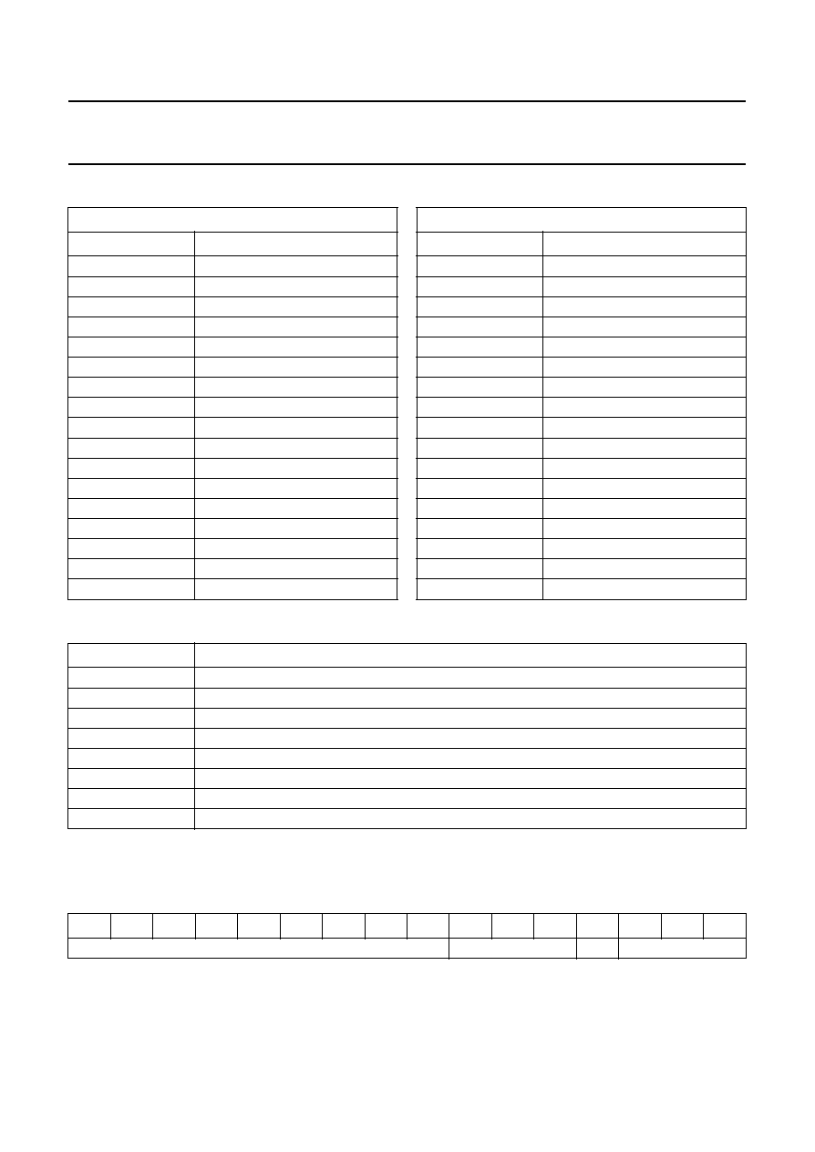
1996 Oct 29
87
Philips Semiconductors
Objective specification
GSM signal processing IC
PCF5083
Table 59 Registers that may be read (see Table 58)
REGISTER
NUMBER
NAME
0
pxs0
1
pxs1
2
pys0
3
pys1
4
sas
5
eas
6
dcuc
7
acuc
8
sp
9
iopc
10
iopcx
11
sioc
12
soym
13
iopf
14
eb
15
reserved
16
mc
Table 60 Registers that may be changed (see Table 58)
REGISTER
NUMBER
NAME
0
pxs0
1
pxs1
2
pys0
3
pys1
4
sas
5
eas
6
dcuc
7
acuc
8
sp
9
iopc
10
iopcx
11
sioc
12
soym
13
siyc
14
soyc
15
ecb
16
mc
Table 61 Determination of the attenuation routine (see Table 58); note 1
Note
1. After reset att is initialized with zero.
Table 62 Operation_mode fields
att
DESCRIPTION
0
no side tone
1
3 dB attenuation
2
6 dB attenuation
3
9 dB attenuation
4
12 dB attenuation
5
15 dB attenuation
6
18 dB attenuation
-
1
loop back test microphone to loud speaker
15
14
13
12
11
10
9
8
7
6
5
4
3
2
1
0
don't care
ATT
HF
TMODE

1996 Oct 29
88
Philips Semiconductors
Objective specification
GSM signal processing IC
PCF5083
9.3.2
P
ERFORMANCE OF
GSM
BASEBAND PROCEDURES
The performance of the PCF5083 GSM baseband procedures is specified within this section.
All performances are valid for the following conditions; unless otherwise specified. However, performance figures are
only preliminary or must be fixed respectively.
·
AGC and quantization in accordance with Fig.16
·
Receiver input noise (AWGN);
-
111 dBm
·
IF filter with a frequency characteristic as shown in Fig.20
·
Constant frequency offset (df) in baseband signal;
-
100 Hz
df
100 Hz
·
Gain mismatch in I and Q path less than 0.5 dB
·
Phase error less than 2
°
·
Channel models in accordance with
"GSM Rec. 05.05".
9.3.2.1
Usable receiver input level range
Table 63 Usable receiver input level range
SYMBOL
PARAMETER
CONDITION
MAX.
UNIT
NER1
nominal error rate; TCH/FS class II
static;
-
10 dBm
2
×
10
-
5
-
NER2
nominal error rate; TCH/FS class II
static;
-
50 dBm
2
×
10
-
5
-
NER3
nominal error rate; TCH/FS class II
static;
-
85 dBm
2
×
10
-
5
-
NER4
nominal error rate; TCH/FS class II
EQ50;
-
40 dBm
2.5
%
NER5
nominal error rate; TCH/FS class II
EQ50;
-
85 dBm
2.5
%
Fig.20 Frequency response of the IF filter.
handbook, halfpage
0
500
0
-
100
-
80
-
60
-
40
-
20
MGE298
100
200
300
400
gain
(dB)
frequency (kHz)
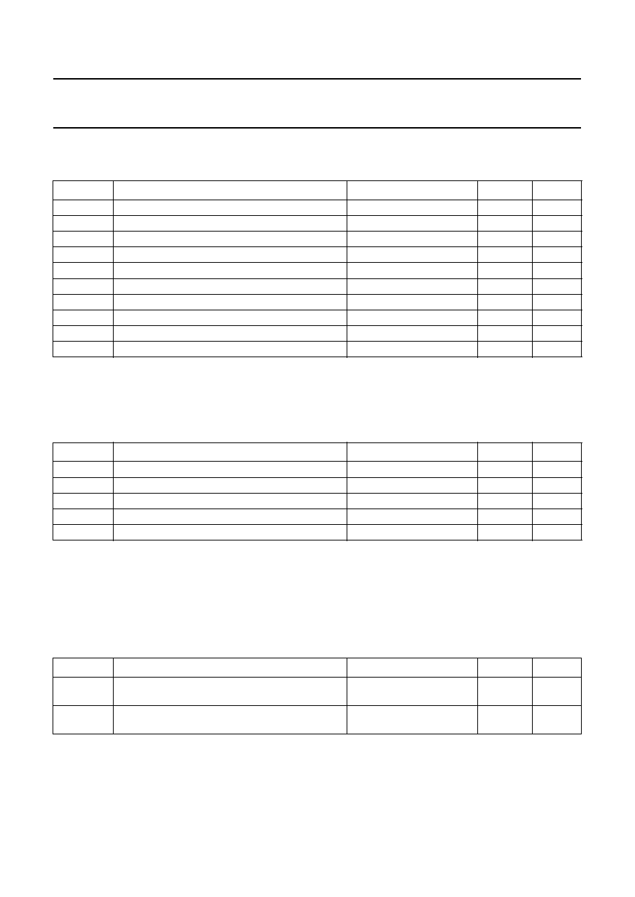
1996 Oct 29
89
Philips Semiconductors
Objective specification
GSM signal processing IC
PCF5083
9.3.2.2
Sensitivity
Table 64 Equalizer and channel decoder sensitivity; note 1
Note
1. Input level:
-
102 dBm.
9.3.2.3
Co-channel rejection
Table 65 Equalizer and channel decoder co-channel rejection; note 1
Note
1. Signal levels:
a) Level of wanted signal
-
85 dBm.
b) Level of unwanted signal
-
94 dBm.
9.3.2.4
Erroneous frame indication performance
Table 66 Equalizer and channel decoder erroneous frame indication performance
SYMBOL
PARAMETER
CONDITION
MAX.
UNIT
FER1
frame erasure rate
static; ideal FH
5
×
10
-
4
-
RBER6
residual bit error rate; TCH/FS class Ib
static; ideal FH
0.2
%
RBER7
residual bit error rate; TCH/FS class II
static; ideal FH
0.5
%
FER2
frame erasure rate
TU50; no FH
4.0
%
RBER3
residual bit error rate; TCH/FS class Ib
TU50; no FH
0.2
%
RBER4
residual bit error rate; TCH/FS class II
TU50; no FH
5.0
%
RBER5
residual bit error rate; TCH/FS class II
RA250; no FH
6.0
%
RBER6
residual bit error rate; TCH/FS class II
HT100; no FH
7.0
%
FER3
frame erasure rate; FACCH
TU50; no FH
6.0
%
FER4
frame erasure rate; SCH
TU50; no FH
13.0
%
SYMBOL
PARAMETER
CONDITION
MAX.
UNIT
FER5
frame erasure rate, TCH/FS
TU3; no FH
15.0 (2.0)
%
RBER7
residual bit error rate; TCF/FS class Ib
TU3; no FH
1.0 (0.1)
%
RBER8
residual bit error rate; TCF/FS class II
TU3; no FH
3.0 (6.0)
%
FER6
frame erasure rate; FACCH
TU3; no FH
18.0
%
FER7
frame erasure rate; SCH
TU50; no FH
14.0
%
SYMBOL
PARAMETER
CONDITION
MAX.
UNIT
FDR1
false detection rate of FACCH, SACCH or SDCCH
random RF input;
level =
-
95 dBm
tbf
-
FDR2
false detection rate of TCH/FS
random RF input;
level =
-
95 dBm
0.1
%

1996 Oct 29
90
Philips Semiconductors
Objective specification
GSM signal processing IC
PCF5083
9.4
Software applications
This section contains examples for several basic GSM
channels. For every example the procedures to be
executed within the DSP are shown in the form of tables.
The first column contains the TDMA frame number fn in
which the EXEC_PROC messages should be sent to the
DSP. The 2nd column shows the corresponding
procedures with all parameters. Parameters in uppercase
are constants, lowercase parameters are variables. The
3rd column contains the number words N
W
to be
transmitted to the DSP within frame fn (PACKET message
assumed). The columns RX and MX contain the number of
I and Q pairs to be sampled in the receive and monitoring
timeslots of TDMA frame fn. Column TX contains the
number of bits to sent to the GMSK modulator within the
transmit timeslot. The tables are based upon the general
rule that an EXEC_PROC message for a procedure that
starts execution in TDMA frame n has to be sent in TDMA
frame N
-
1.
Unless otherwise noted, the corresponding
PROC_RETURN message will be available at the latest at
the end of TDMA frame N+1, i.e. if the messages are read
by the SC at beginning of every TDMA frame, the
PROC_RETURN message will be available in frame
N + 2. Start and end of a TDMA frame are defined by the
falling edge of the FRAME_INT signal produced by the
timer core.
9.4.1
R
ECEIVING A
CCH
BLOCK
Table 67 shows how to receive a CCH block and to
perform monitoring of two neighbouring cells in parallel. It
is assumed that the CCH block has to be received in the
frames N to N + 3. Note that the TX timeslot is used for
monitoring in this example.
Table 67 Procedures to be started for receiving a CCH block
Note
1. Procedures to be started via EXEC_PROC in TDMA frame FN.
fn
PROCEDURES
(1)
N
W
RX
TX
MX
N
-
1
CP_rx_normal_burst (CCH_CMI_BUFF1, tsc, agc_gain1);
CP_power_measure (agc_gain2)
CP_power_measure (agc_gain3)
15
-
-
-
N
CP_rx_normal_burst (CCH_CMI_BUFF2, tsc, agc_gain1);
CP_power_measure (agc_gain2)
CP_power_measure (agc_gain3)
15
149
80
80
N + 1
CP_rx_normal_burst (CCH_CMI_BUFF3, tsc, agc_gain1);
CP_power_measure (agc_gain2)
CP_power_measure (agc_gain3)
15
149
80
80
N + 2
CP_rx_normal_burst (CCH_CMI_BUFF4, tsc, agc_gain1);
CM_decoder_CCH( );
CP_power_measure (agc_gain2)
CP_power_measure (agc_gain3)
18
149
80
80
N + 3
-
-
149
80
80

1996 Oct 29
91
Philips Semiconductors
Objective specification
GSM signal processing IC
PCF5083
9.4.2
T
RANSMITTING A
CCH
BLOCK
This example shows how to transmit a CCH block. The transmission is performed in the TDMA frames N to N + 3. Only
one message has to be sent in order to transmit a CCH block.
Table 68 Procedures to be started for transmitting a CCH block
Note
1. Procedures to be started via EXEC_PROC in TDMA frame FN.
9.4.3
FB
SEARCH FOR TIMING SYNCHRONIZATION
This example shows how to achieve time synchronization when the mobile is in IDLE mode or is on a channel with a
51 multiframe structure.
Table 69 Procedures to be started for FB search for timing synchronization
Note
1. Procedures to be started via EXEC_PROC in TDMA frame FN.
fn
PROCEDURES
(1)
N
W
RX
TX
MX
N
-
1
CP_tx_CCH (tsc, cch_msg)
15
-
-
-
N
-
-
-
156
-
N + 1
-
-
-
156
-
N + 2
-
-
-
156
-
N + 3
-
-
-
156
-
fn
PROCEDURES
(1)
N
W
RX
TX
MX
N
FB_search_fcb_init(15)
FB_search_fcb( )
9
-
-
-
N+11, N+22
FB_search_fcb( )
5
-
-
-
N+1, N+12, N+23
-
-
-
1404
N+2, N+13, N+24
FB_search_fcb( )
5
-
-
N+3, N+14, N+25
-
-
-
1404
N+4, N+15, N+26
FB_search_fcb( )
5
-
-
N+5, N+16, N+27
-
-
-
1404
N+6, N+17, N+28
FB_search_fcb( )
5
-
-
N+7, N+18, N+29
-
-
-
1404
N+8, N+19, N+30
FB_search_fcb( )
5
-
-
N+9, N+20, N+31
-
-
-
1404
N+10, N+21, N+32
-
-
-

1996 Oct 29
92
Philips Semiconductors
Objective specification
GSM signal processing IC
PCF5083
9.4.4
P
ROCESSING A
TCH/FS
MULTIFRAME
9.4.4.1
Normal mode
Figure 21 depicts the timing diagram of the procedure execution timing for a TCH/FS multiframe. Table 70 shows the
procedures to be executed within the DSP for processing of a TCH/FS multiframe in normal mode. It is assumed that an
even numbered time slot is assigned.
Table 70 Procedures to be executed for processing a TCH/FS multiframe in normal mode
FN MOD 26
PROCEDURES
N
W
RX
TX
MX
0
CP_rx_normal_burst (TCH_CMI_BUFF2, tsc, agc_gain)
CP_power_measure (agc_gain1)
MP_audio_sync(2, 2)
17
149
156
80
4, 13, 17
CP_rx_normal_burst (TCH_CMI_BUFF2, tsc, agc_gain)
CP_power_measure (agc_gain1)
12
149
156
80
8
{CM_encoder_CCH (cch_msg[12])}; note 1
CP_rx_normal_burst (TCH_CMI_BUFF2, tsc, agc_gain)
CP_rx_normal_burst (CCH_INFO_BUFFi, tsc)
CP_power_measure (agc_gain1)
32
149
156
80
21
CP_rx_normal_burst (TCH_CMI_BUFF2, tsc, agc_gain)
CI_encrypt (SCRATCH_BUFF1); note 2
CP_power_measure (agc_gain1)
17
149
156
80
1, 5, 9, 14, 18,
22
CP_rx_normal_burst (TCH_CMI_BUFF3, tsc, agc_gain)
CP_tx_speech (dtx, bpf, tm, taf, tsc, ff, fm[12])
CP_power_measure (agc_gain1)
33
149
156
80
2, 6, 10, 15, 19 CP_rx_normal_burst (TCH_CMI_BUFF4, tsc, agc_gain)
CP_rx_speech (dtx_flag, taf, test_mode)
CP_power_measure (agc_gain1)
18
149
156
80
3, 7, 12, 16, 20 CP_rx_normal_burst (TCH_CMI_BUFF1, tsc, agc_gain)
CP_power_measure (agc_gain1)
12
149
156
80
11
CP_rx_normal_burst (CCH_CMI_BUFF1, tsc, agc_gain)
[CM_decoder_CCH( )]; note 3
CP_power_measure (agc_gain1)
14
149
156
80

1996 Oct 29
93
Philips Semiconductors
Objective specification
GSM signal processing IC
PCF5083
Notes
1. CM_encoder_CCH is only called, if the current multiframe contains the 1st SACCH sub-block.
2. Dummy encryption to increment TDMA frame counters (skip Idle frame).
3. CM_decoder_CCH is only called, if the current multiframe contains the 4th SACCH sub-block.
4. If the BCCh identification of the neighbouring cells is not required in a certain idle frame, then up to 3 level
measurements can be performed in that frame.
5. Dummy encryption to increment TDMA frame counter (skip idle frame).
6. Monitoring of a frequency correction burst from a neighbouring cell.
7. Decoding of a synchronization burst from a neighbouring cell.
23
start of
FB monitoring
CP_rx_normal_burst (TCH_CMI_BUFF4, tsc, agc_gain)
FB_search_FCB_INT (n_int, threshold)
FB_search_FCB( )
CP_rx_speech (dtx_flag, taf, test_mode)
22
149
156
80
23
continue
FB monitoring
CP_rx_normal_burst (TCH_CMI_BUFF4, tsc, agc_gain)
FB_search_FCB( )
CP_rx_speech (dtx_flag, taf, test_mode)
17
149
156
80
23
decode SCh
CP_rx_normal_burst (TCH_CMI_BUFF4, tsc, agc_gain)
CP_rx_speech (dtx_flag, taf, test_mode)
CP_rx_SCH( )
17
149
156
80
23
level
measurement
CP_rx_normal_burst (TCH_CMI_BUFF4, tsc, agc_gain)
CP_rxlev3 (agc_gain1, agc_gain2, agc_gain3); note 4
CP_rx_speech (dtx_flag, taf, test_mode)
20
149
156
80
24
CI_decrypt (SCRATCH_BUFF,1); note 5
0
149
156
1404
(6)
or 167
(7)
25
CP_rx_normal_burst (TCH_CMI_BUFF1, tsc, agc_gain)
CP_power_measure (agc_gain1)
17
80 or 0
80 or 0
80 or 0
FN MOD 26
PROCEDURES
N
W
RX
TX
MX
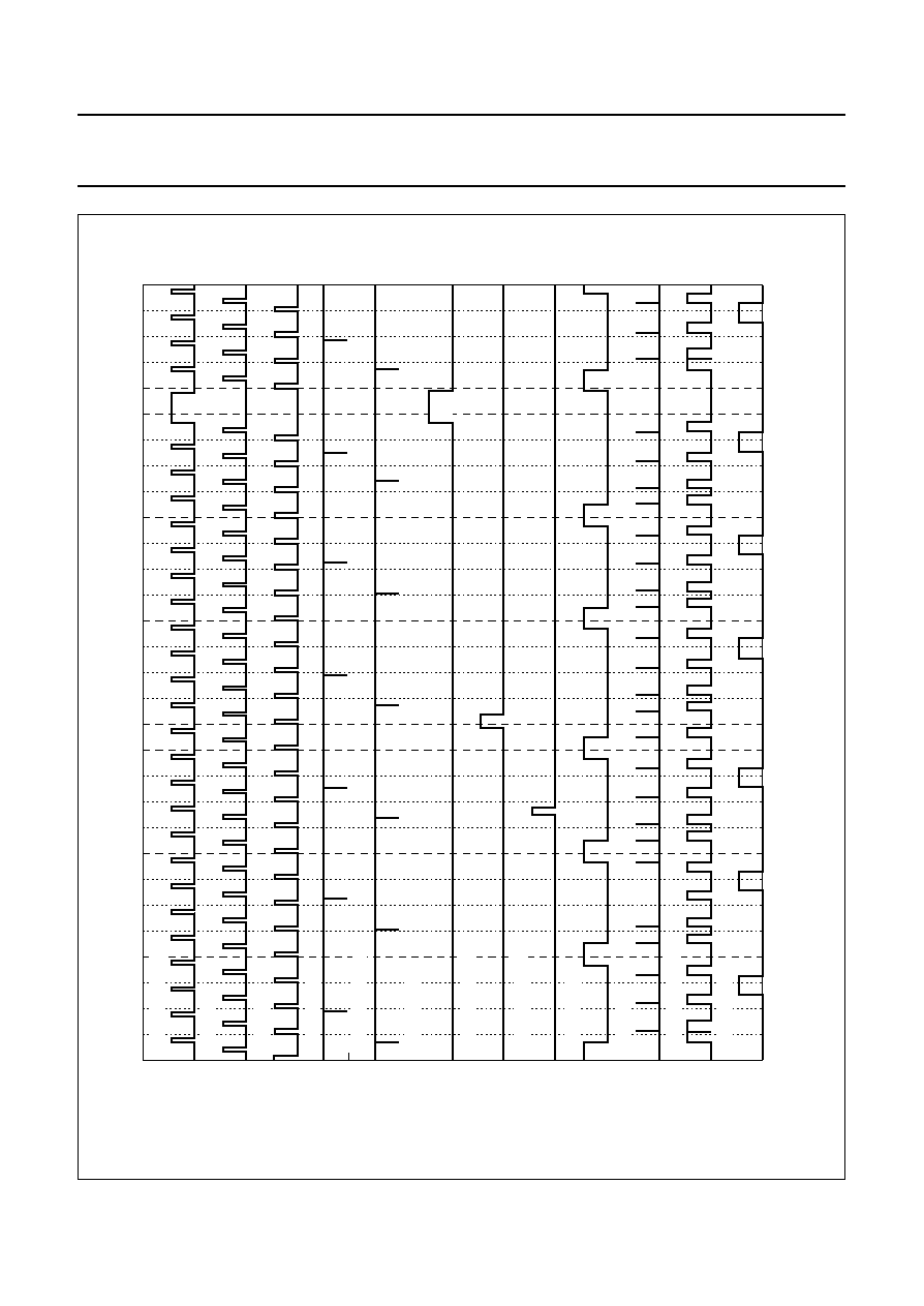
1996 Oct 29
94
Philips Semiconductors
Objective specification
GSM signal processing IC
PCF5083
handbook, full pagewidth
MGE299
0
2
4
6
8
10
12
0
5
15
20
25
30
10
TDMA frame number (fn)
timeslot
monitoring timeslot
tx timeslot
rx timeslot
audio input frame
audio output frame
FB_search_fcb
CM_decoder_CCH
CM_encoder_CCH
CP_rx_speech
CP_rxlev1
CP_rx_normal_burst
CP_tx_speech
Fig.21 Procedure execution timing for TCH/FS.

1996 Oct 29
95
Philips Semiconductors
Objective specification
GSM signal processing IC
PCF5083
9.4.4.2
Loop-back mode
During TCH_LOOP mode the CP_TX_SPEECH and
CP_RX_SPEECH procedures have to be replaced by the
following procedures:
·
Replacement for CP_tx_speech:
MP_read_audio_in_fifo (SCRATCH_BUFF, 160)
DB_copy_buffer (TCH_LOOP_BUFF,
SCRATCH_BUFF, 0, 0, 82)
CM_convert_tchfs_data(bfi_sig_flag)
CM_encoder_tchfs(dtx_flag, taf, facch_flag,
facch_msg[12])
CP_tx_four_normal_bursts (tsc)
·
Replacement for CP_rx_speech:
CM_decoder_tchfs( )
DB_copy_buffer(SCRATCH_BUFF,
TCH_LOOP_BUFF, 0, 0, 82)
DB_fill_buffer(SCRATCH_BUFF, 0, 0, 160)
MP_write_audio_out_fifo(SCRATCH_BUFF, 160).
9.4.4.3
Initialization messages for normal mode
Before the first TDMA frame of a TCH/FS can be
processed, several initialization messages have to be sent
to the DSP. Initialization is done in 2 DMA frames as
shown in Table 72.
The first one or two results of CM_decoder_TCH are
based on only partially observed input data, since
8 successive normal bursts are needed due to
interleaving.
Table 71 Parameter nb
nb
t2
s
4
0
4
8
13
17
21
25
3
1
5
9
14
18
22
10
2
2
6
-
15
19
23
-
5
3
7
12
16
20
24
-
6
11
-
-
-
-
-
-
Table 72 Initialization messages
Table 73 Initialization procedures
Notes
1. Procedures to be started via EXEC_PROC in TDMA frame FN (TCH/FS normal mode).
2. t1
s
= FN
s
divided by 26
×
51;
t2
s
= FN
s
modulo 26;
t3
s
= FN
s
modulo 51.
3. The parameter nb determines the number of normal bursts to be written into the modulator output FIFO in the
initialization frame. It depends on the frame number of the 1st processed frame in accordance with Table 71.
TDMA
FRAME
EXPLANATION
FN
s
-
2
In this TDMA frame the message for initialization of speech CODEC, channel CODEC and ciphering are
sent to the DSP. Furthermore the modulator out FIFO is filled with the proper number of bursts and
synchronization between TDMA frame timing and speech frame timing is performed and the audio
interface is enabled by setting the IO1 pin. No data is received or transmitted within this frame.
FN
s
-
1
In this TDMA frame the EXEC_PROC messages for the procedures processing the data of frame FN
s
are sent to the DSP. No data is received or transmitted within this frame.
FN
s
In this TDMA frame the normal processing of receive and transmit data takes place.
fn
PROCEDURES
(1)
N
W
RX
TX
MX
FN
s
-
2
CP_start_TCHFS (enc_flag, dec_flag, t1
s
, t2
s
, t3
s
, kc[4], nb); notes 2 and 3
DB_write_register (11, 0x0100, 1); set IO1 = 1
21
0
0
0
FN
s
-
1
The correct value for N
W
must be looked-up in Table 70
`...'
0
0
0
FN
s
The correct value for N
W
must be looked up in Table 70
`...'
149
164
151

1996 Oct 29
96
Philips Semiconductors
Objective specification
GSM signal processing IC
PCF5083
9.4.4.4
Handover mode
Table 74 shows the procedures to be executed within the DSP for processing of a TCH/FS multiframe in Handover mode.
Table 74 Procedures to be executed for processing a TCH/FS multiframe in handover mode
Notes
1. Dummy encryption to increment TDMA frame counters (skip Idle + SACCH frame).
2. CM_DECODER_CCH is only called, if the current multiframe contains the 4th SACCH sub-block.
3. Dummy encryption to increment TDMA frame counters (skip Idle frame).
FN MOD 26
PROCEDURES
N
W
RX
TX
MX
0, 4, 13, 17
CP_tx_RACH (bsic, rach_msg)
CP_rx_normal_burst (TCH_CMI_BUFF2, tsc, agc_gain)
CP_power_measure (agc_gain1)
12
149
156
80
8, 21
CP_tx_RACH (bsic, rach_msg)
CP_rx_normal_burst (TCH_CMI_BUFF2, tsc, agc_gain)
CI_encrypt (SCRATCH_BUFF,1); note 1
CP_power_measure (agc_gain1)
12
149
156
80
1, 5, 9, 14, 18,
22
CP_tx_RACH (bsic, rach_msg)
CP_rx_normal_burst (TCH_CMI_BUFF3, tsc, agc_gain)
CI_encrypt (SCRATCH_BUFF, 4)
MP_read_audio_in_fifo (SCRATCH_BUFF, 160)
CP_power_measure (agc_gain1)
33
149
156
80
2, 6, 10, 15,
19, 23
CP_tx_RACH (bsic, rach_msg)
CP_rx_normal_burst (TCH_CMI_BUFF4, tsc, agc_gain)
DB_fill_buffer (SCRATCH_BUFF,0,0,160)
MP_write_audio_out_fifo (SCRATCH_BUFF, 160)
CM_decoder_TCH (dtx_flag, taf, test_mode)
CP_power_measure (agc_gain1)
18
149
156
80
3, 7, 12, 16, 20 CP_tx_RACH (bsic, rach_msg)
CP_rx_normal_burst (TCH_CMI_BUFF1, tsc, agc_gain)
CP_power_measure (agc_gain1)
12
149
156
80
11
CP_tx_RACH (bsic, rach_msg)
CP_rx_normal_burst (CCH_CMI_BUFFi, tsc, agc_gain)
[CM_decoder_CCH( )]; note 2
CP_power_measure (agc_gain1)
14
149
156
80
24
CP_tx_RACH (bsic, rach_msg)
CI_decrypt (SCRATCH_BUFF,1); note 3
15
149
156
80
25
CP_tx_RACH (bsic, rach_msg)
CP_rx_normal_burst (TCH_CMI_BUFF1, tsc, agc_gain)
CP_power_measure (agc_gain1)
12
-
156
-

1996 Oct 29
97
Philips Semiconductors
Objective specification
GSM signal processing IC
PCF5083
9.4.4.5
Initialization messages for Handover mode
Table 75 shows how a handover from TCH/FS to another TCH/FS has to be processed. `fn
H
' is the first frame transmitted
on the new TCH/FS in Handover mode (handover access burst transmitted in uplink). `fn
S
' is the first frame processed
in normal mode on the new TCH/FS (normal burst in up link).
Table 75 Initialization procedures for handover mode
Notes
1. Procedures to be started via EXEC_PROC in TDMA frame FN (TCH/FS normal mode).
2. t1
s
= FN
s
divided by 26
×
51;
t2
s
= FN
s
modulo 26;
t3
s
= FN
s
modulo 51.
3. The parameter nb determines the number of normal bursts to be written into the modulator output FIFO in the
initialization frame. It depends on the frame number of the 1st processed frame in accordance with Table 71.
fn
PROCEDURES
(1)
N
W
RX
TX
MX
.
procedure calls for TCH/FS in normal mode; the correct value for N
W
must be
looked-up in Table 70.
`...'
149
156
80
.
.
.
.
.
.
.
procedure calls for TCH/FS in normal mode; the correct value for N
W
must be
looked-up in Table 70.
`...'
149
156
80
.
-
0
149
156
80
fn
H
-
2
CP_start_TCHFS (enc_flag, dec_flag, t1
s
, t2
s
, t3
s
, kc[4], nb); notes 2 and 3
MP_exec_reset (MOD_OUT_FIFO);
DB_write_register(11, 0x0100, 1); set IO1 = 1
21
0
0
0
fn
H
-
1
procedure calls for TCH/FS in handover mode; the correct value for N
W
must
be looked-up in Table 70.
`...'
0
0
0
fn
H
procedure calls for TCH/FS in handover mode; the correct value for N
W
must
be looked-up in Table 70.
`...'
149
156
80
.
procedure calls for TCH/FS in handover mode; the correct value for N
W
must
be looked-up in Table 70.
`...'
149
156
80
fn
s
-
2
procedure calls for TCH/FS in handover mode
BB_normal_burst (SCRATCH_BUFF,SCRATCH_BUFF, tsc,
nb)MP_write_normal_bursts (SCRATCH_BUFF, nb); note 3
29
149
156
80
fn
s
-
1
procedure calls for TCH/FS in normal mode; the correct value for N
W
must be
looked-up in Table 70.
`...'
149
156
80
fn
s
procedure calls for TCH/FS in normal mode; the correct value for N
W
must be
looked-up in Table 70.
`...'
149
156
80

1996 Oct 29
98
Philips Semiconductors
Objective specification
GSM signal processing IC
PCF5083
9.5
Instruction Set
Details concerning the PCF5083 Instruction Set can be found in the
"PCF5082 Information manual". Some exceptions
that apply to the PCF5083 are listed below:
·
Moves from RAM using pointers to I/O control registers (iopc, iopcx and sioc) are not recommended due to reliability
problems. Load immediate from program memory to these registers should be performed. Otherwise, access to the
I/O control registers could be performed via secondary registers e.g.
bm = *px0++ followed by sioc = bm
·
All code segments using pp pointer as source must be within a disable/enable pair if interrupts are enabled e.g. disable;
.....
bm = *pp++;
.....
·
The instruction *px0++ is illegal. Instead, use the following sequence with consideration to the point above:
dr = *pp++;
*px0++ = dr;
·
The instruction `.... = *pp++' may be located in any PROM bank (including the mirrored PROM07 at location
XF800H to XFFFF0. However, the instruction will not work if located in any of the RAM banks mapped to program
address space.
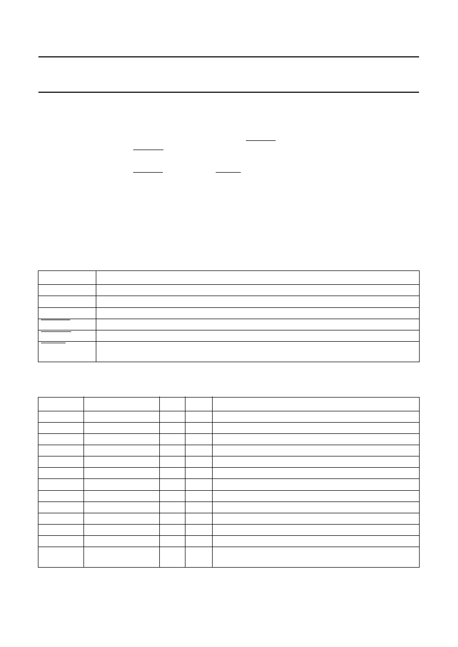
1996 Oct 29
99
Philips Semiconductors
Objective specification
GSM signal processing IC
PCF5083
10 MICROCONTROLLER INTERFACE
The PCF5083 includes a standard 68000 compatible microcontroller interface. The interface consists of the lines
specified in Table 76.
The 128-byte wide register space of the Timer core is selected if HCEN_T is asserted. The 4 byte wide register space
of the DSP core is selected if HCEN_D is asserted. The DSP core only uses the address lines HA0 and HA1. All other
address lines are don't care for the DSP core.
The Timer core accessed via HCEN_T does not assert DTACK.
Registers wider than 8-bit are aligned on word boundaries with the MSB on the lowest address and the LSB on the
highest address. For registers which use only three byte addresses, a reserved address location is provided to make
these registers accessible as longwords.
Reserved address locations, write only bits or registers and unused bits within registers are read as zeros and don't care
for write operations.
For the DSP Core refer to Section 9.1.6.
Table 76 The Interface signal lines
10.1
Register Set for the Timer Core
Table 77 Register set
SIGNAL
DESCRIPTION
HD0 to HD7
8-bit bidirectional data bus.
HA0 to HA6
7-bit unidirectional address bus.
HR/W
Read/write select line. A logic 0, writes to the PCF5083. A logic 1, reads from the PCF5083.
HCEN_T
Chip select line for the Timer core (active LOW).
HCEN_D
Chip select line for the DSP core (active LOW).
DTACK
DSP core data acknowledge line (connected to the DTACK input of a 68000 compatible
microcontroller.
OFFSET
REGISTER
SIZE
R/W
(1)
DESCRIPTION
00, 01
MODE0_REG
14
R/W
Mode Control Register 0; see Table 78
02, 03
MODE1_REG
14
R/W
Mode Control Register 1; see Table 78
04
RXBURST0_REG
8
W
RXON length in bit
05
RXBURST1_REG
8
W
RXON length in bit
06
RXBURST2_REG
8
W
RXON length in bit
07
TXBURST0_REG
8
W
TXON length in bit
08
TXBURST1_REG
8
W
TXON length in bit
09
TXBURST2_REG
7
W
Start of the Rx burst in QB
0A, 0B
TXSTART_REG
11
W
Start of the TX burst in QB
0C, 0D
MONSTART_REG
13
W
Start of the MON burst in QB
0E, 0F
TXKEY0_REG
10
W
TXKEY0 length in QB
10, 11
TXKEY1_REG
10
W
TXKEY1 length in QB
12
GPON1_REG
6
W
Time of GPON1 getting active in TDMA frames before the end
of the Sleep mode

1996 Oct 29
100
Philips Semiconductors
Objective specification
GSM signal processing IC
PCF5083
13
GPON2_REG
6
W
Time of GPON2 getting active in TDMA frames before the end
of the Sleep mode
14
reserved
-
-
-
15
DSPON_REG
6
W
Time of DSPON getting active in TDMA frames before the end
of the Sleep mode
16
REFON_REG
6
W
Time of (N)REFON getting active in TDMA frames before the
end of the Sleep mode
17
PDRX1_REG
5
W
Time of PDRX1 getting active in 32 QB before RXON active
18
PDRX2_REG
5
W
Time of PDRX2 getting active in 32 QB before RXON active
19
PDTX1_REG
W
Time of PDTX1 getting active in 32 QB before TXON active
1A
PDTX2_REG
W
Time of NPDTX2 getting active in 32 QB before TXON active
1B
PDBIAS_REG
W
Time of PDBIAS getting active in 32 QB before TXON active
1C
PDSYN_REG
W
Time of PDSYN getting active in 32 QB before RXON/TXON
active
1D
AGCSTART_REG
W
Time of DACON_REG to be sent in 32 QB before RXON active
1E
PDDELAY_REG
6
W
PDTX1, NPDTX2 and PDSYN inactive to TXKEY1 inactive
delay in QB
1F
KEYOFF_REG
6
W
TXKEY2 inactive to TXKEY1 inactive delay in QB
20, 21
KEYON2_REG
9
W
TXKEY2 active to TXON active delay in QB
22, 23
KEYON1_REG
9
W
TXKEY1 active to TXON active delay in QB
24, 25
POL_REG
14
R/W
Polarity of Power-Down Control Lines; see Table 79
26, 27
MASK_REG
15
R/W
Bit mask register for Power-Down Control Lines; see Table 80
28
QBCCTRL_REG
8
R/W
Quarterbit counter control register; see Table 81
29
SQBCINC_REG
8
R
Sleep quarterbit counter increment
STOP_REG
8
W
Stop OFF-Timer with data value A5H
2A, 2B
QBC_REG
15
R
QBC access for synchronization
13
W
R: read 15-bit quarterbit counter (
1
/
4
QB resolution)
W: write 13-bit synchronization value (1 QB resolution)
2C, 2D
SLEEPCNT_REG
9
W
Number of TDMA frames to sleep
FRAMECNT_REG
9
R
Duration of last Sleep mode period in TDMA frames
2E, 2F
HWCTRL_REG
11
R/W
Hardware Control Register; see Table 82
30 to 3F
-
-
R/W
Real Time Clock registers; see Table 83
3E
reserved
-
-
-
3F to 41
RX_REG
17
W
RF Bus: RX frequency
42
reserved
-
-
-
43 to 45
TX_REG
17
W
RF Bus: TX frequency
46
reserved
-
-
-
47. to 49
MON_REG
17
W
RF Bus: MON frequency
4A
reserved
-
-
-
4B to 4D
RXGAIN_REG
18
W
RF Bus: RX gain
4E
reserved
-
-
-
4F to 51
TXGAIN_REG
18
W
RF Bus: Gain setting for a MON burst during the TX timeslot
OFFSET
REGISTER
SIZE
R/W
(1)
DESCRIPTION

1996 Oct 29
101
Philips Semiconductors
Objective specification
GSM signal processing IC
PCF5083
Notes
1. R = read only; W = write only; R/W = read and write.
2. The flags of register IOMCON_REG should not be changed as long as the interface is enabled with
CLOCK_MODE = 0 to prevent an unpredictable behaviour of the interface.
52
reserved
-
-
-
53 to 55
MONGAIN_REG
18
W
RF Bus: MON gain
56, 57
DAC0_REG
16
W
Gain DAC value 0
58, 59
DAC1_REG
16
W
Gain DAC value 1
5A, 5B
DACON_REG
16
W
Gain DAC power-up value
5C, 5D
DACOFF_REG
16
W
Gain DAC power-down value
5E
reserved
-
-
-
5E to 61
IMCIN_REG
21
R
IMC data in
IMCOUT_REG
28
W
IMC data out
62
MSB_REG
4
R/W
Gain Control Channel MSB Register
0: DAC0_REG bit 16
1: DAC1_REG bit 16
2: DACON_REG bit 16
3: DACOFF_REG bit 16
63
RFCTRL0_REG
8
W
RF bus control register 0
64
RFCTRL1_REG
8
W
RF bus control register 1
65
RFCTRL2_REG
8
W
RF bus control register 2
66
RFCTRL3_REG
8
W
RF bus control register 3
67
COMBINT_REG
6
R/W
Combined interrupt register; see Table 84
68
HIPRINT_REG
8
R/W
High priority interrupt register; see Table 85
69
HIPRMASK_REG
8
R/W
High priority interrupt mask register; see Table 86
6A
SIINT_REG
6
R
Serial interface interrupt register; see Table 87
6B
SIMASK_REG
5
R/W
Serial interface interrupt mask register; see Table 88
6C, 6D
IOMCON_REG
(2)
16
R/W
IOM
®
-2 interface configuration register; see Table 89
6E, 6F
ACON_REG
13
R/W
Audio Interface configuration register; see Table 90
70
RXD_REG
8
R
RS232 data input register
TXD_REG
8
W
RS232 data output register
71
MON0_REG
8
R/W
IOM
®
-2 interface monitor 0 data register
72
MON1_REG
6
R/W
IOM
®
-2 interface monitor 1data register
73
CI0_REG
6
R/W
IOM
®
-2 interface C/I 0 data register
74
CI1_REG
6
R/W
IOM
®
-2 interface C/I 1 data register
75
IOMFLAG_REG
8
R
IOM
®
-2 interface interrupt flag register; see Table 91
76
IOMCTRL_REG
8
R/W
IOM
®
-2 interface control register; see Table 92
77
IOMEN_REG
8
R/W
IOM
®
-2 interface interrupt enable register, see Table 93
78
PORTDATA_REG
6
R/W
Parallel port data register; see Table 94
79
PORTDDIR_REG
6
R/W
Parallel port data direction register; see Table 95
7A
SYSCON_REG
7
R/W
System configuration register; see Table 96
OFFSET
REGISTER
SIZE
R/W
(1)
DESCRIPTION
1996 Oct 29
102
Philips Semiconductors
Objective specification
GSM signal processing IC
PCF5083
Table 78 Mode Control Registers 0 and 1
Note
1. RSTx = 0 means reset condition if either RSTO or RSTC is asserted; `
-
' denotes not affected from reset line.
During reset (RST, RSTO, RSTC) only those registers with an explicitly given reset value are affected. All other
registers are undefined and have to be set by the controller.
Table 79 Polarity Register (Power-Down Control Lines)
Note
1. RSTx = 0 means reset condition if either RSTO or RSTC is asserted; `
-
'denotes not affected from reset line.
During reset (RST, RSTO, RSTC) only those registers with an explicitly given reset value are affected. All other
registers are undefined and have to be set by the controller.
BIT
R/W
SYMBOL
OPERATION (if bit is set)
RST = 0
RSTx = 0
(1)
0
R/W
RECRX
Generate the Rx burst timing
0
-
1
R/W
RECTX
Generate the MON burst timing during the TX timeslot
0
-
2
R/W
RECMON
Generate the MON burst timing
0
-
3
R/W
RECON
Generate the idle frame timing
0
-
4
R/W
SEND
Generate the TX burst timing
0
-
5
R/W
DTX
Enable DTX mode
0
-
6
R/W
RXLENGTH0
Select RXLENGTHx_REG for the Rx burst
0
-
7
R/W
RXLENGTH1
0
-
8
R/W
MONLENGTH0
Select RXLENGTHx_REG for the MON burst
0
-
9
R/W
MONLENGTH1
0
-
10
R/W
TXLENGTH
Select TXLENGTHx_REG for the TX burst
0
-
11
R/W
RXCAL
Generate the RX calibration timing
0
-
12
R/W
DISFRAMEINT
Disable the frame interrupt
0
-
13
R/W
USEMODE
Select MODEx_REG for the next frame
0
-
BIT
R/W
SYMBOL
OPERATION (if bit is set)
RST = 0
RSTx = 0
(1)
0
R/W
PDRX1
Enable line has default polarity if its corresponding bit
is a logic 0. Enable line has inverse default polarity if its
corresponding bit is a logic 1.
0
-
1
R/W
PDRX2
0
-
2
R/W
NPDTX2
0
-
3
R/W
PDSYN
0
-
4
R/W
TXKEY1
0
-
5
R/W
TXKEY2
0
-
6
R/W
RXON
0
-
7
R/W
TXON
0
-
8
R/W
BEN
0
-
9
R/W
GPON1
0
-
10
R/W
GPON2
0
-
11
R/W
REFON
0
-
12
R/W
DSPON
0
-
13
R/W
NREFON
0
-
1996 Oct 29
103
Philips Semiconductors
Objective specification
GSM signal processing IC
PCF5083
Table 80 Bit mask register (Power-Down Control Lines)
Note
1. RSTx = 0 means reset condition if either RSTO or RSTC is asserted; `
-
' denotes not affected from reset line.
During reset (RST, RSTO, RSTC) only those registers with an explicitly given reset value are affected. All other
registers are undefined and have to be set by the controller.
Table 81 Quarterbit Counter Control Register
Note
1. RSTx = 0 means reset condition if either RSTO or RSTC is asserted; `
-
' denotes not affected from reset line.
During reset (RST, RSTO, RSTC) only those registers with an explicitly given reset value are affected. All other
registers are undefined and have to be set by the controller.
BIT
R/W
SYMBOL
OPERATION (if bit is set)
RST = 0
RSTx = 0
(1)
0
R/W
PDRX1
A logic 1 enables the control line. A logic 0 disables the
control line, output level determined with corresponding
output polarity flag
1
-
1
R/W
PDRX2
1
-
2
R/W
(N)PDTX1,
(N)PDBIAS
1
-
2
R/W
NPDTX2
1
-
3
R/W
PDSYN
1
-
4
R/W
TXKEY1
1
-
5
R/W
TXKEY2
1
-
6
R/W
RXON
1
-
7
R/W
TXON
1
-
8
R/W
BEN
1
-
9
R/W
GPON1
1
-
10
R/W
GPON2
1
-
11
R/W
REFON
1
-
12
R/W
DSPON
1
-
13
R/W
NREFON
1
-
Bit
R/W
SYMBOL
OPERATION (if bit is set)
RST = 0
RSTx = 0
(1)
0
R/W
SYNC
Enable SYNC mode
0
-
1
R/W
INSERT
Enable INSERT mode
0
-
2
R/W
EXTRACT
Enable EXTRACT mode
0
-
3
R/W
SLEEP
Enable Sleep mode
0
-
4
R/W
SLEEPRED
Enable Reduced Sleep mode
0
-
5
R/W
CAL
Start Sleep mode calibration procedure
0
-
6
R/W
FSCEXT
Enable IOM
®
-2 FSC period extension mode
0
-
7
R/W
FSCRED
Enable IOM
®
-2 FSC period reduction mode
0
-
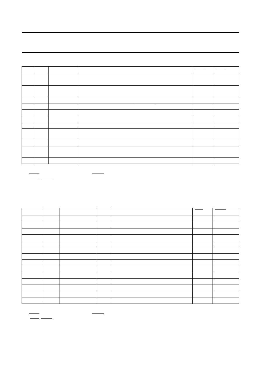
1996 Oct 29
104
Philips Semiconductors
Objective specification
GSM signal processing IC
PCF5083
Table 82 Hardware Control Register
Notes
1. RSTx = 0 means reset condition if RSTO is asserted; `
-
' denotes not affected from reset line. During reset
(RST, RSTO) only those registers with an explicitly given reset value are affected. All other registers are undefined
and have to be set by the controller.
2. To clear these interrupt flags, the corresponding location has to be written with a logic 1.
Table 83 Real Time Clock registers
Note
1. RSTx = 0 means reset condition if RSTC is asserted; `
-
' denotes not affected from reset line. During reset
(RST, RSTC) only those registers with an explicitly given reset value are affected. All other registers are undefined
and have to be set by the controller.
BIT
R/W
SYMBOL
OPERATION (if bit is set)
RST = 0
RSTx = 0
(1)
0
R/W
AUXON_LH
(2)
HWCTRL_INT activated from LOW-to-HIGH transition of
input AUXON
-
0
1
R/W
AUXON_HL
(2)
HWCTRL_INT activated from HIGH-to-LOW transition of
input AUXON
-
0
2
R/W
ONKEY
(2)
HWCTRL_INT activated from ONKEY input
-
0
3
R/W
LOWVOLT
(2)
HWCTRL_INT activated from LOWVOLT input
-
0
4
R/W
CLOCK
(2)
HWCTRL_INT activated from real time clock
-
0
5
R/W
ALARM
(2)
HWCTRL_INT activated from alarm time match
-
0
6
R/W
SWOFF
Set to logic 1 for mobile switch off operation
0
0
7
R/W
SECINT
Select the real time clock interrupt to appear every second or
every minute
0
0
8
R/W
SETCLOCK
Set to logic 1 to enable the real time clock to be set
0
0
9
R/W
MMIREQ
(2)
HWCTRL_INT activated from a MMI controller service
request via input MMIREQ
-
0
10
R/W
MMICLK
A logic 1 enables the MMI controller clock output (MMICLK)
1
1
OFFSET
R/W
SYMBOL
SIZE
DESCRIPTION
RST = 0
RSTx = 0
(1)
30
R/W
SEC_REG
7
RTC: seconds
-
00
31
R/W
MIN_REG
7
RTC: minutes
-
00
32
R/W
HOUR_REG
6
RTC: hours
-
00
33
R/W
DAY_REG
3
RTC: day
-
00
34
R/W
DATE_REG
6
RTC: date
-
01
35
R/W
MONTH_REG
5
RTC: month
-
01
36
R/W
YEAR_REG
8
RTC: year
-
00
37
R/W
SEC_A_REG
7
RTC alarm function: seconds
-
-
38
R/W
MIN_A_REG
7
RTC alarm function: minutes
-
-
39
R/W
HOUR_A_REG
6
RTC alarm function: hours
-
-
3A
R/W
DAY_A_REG
3
RTC alarm function: day
-
-
3B
R/W
DATE_A_REG
6
RTC alarm function: date
-
-
3C
R/W
MONTH_A_REG
5
RTC alarm function: month
-
00
3D
R/W
YEAR_A_REG
8
RTC alarm function: year
-
-
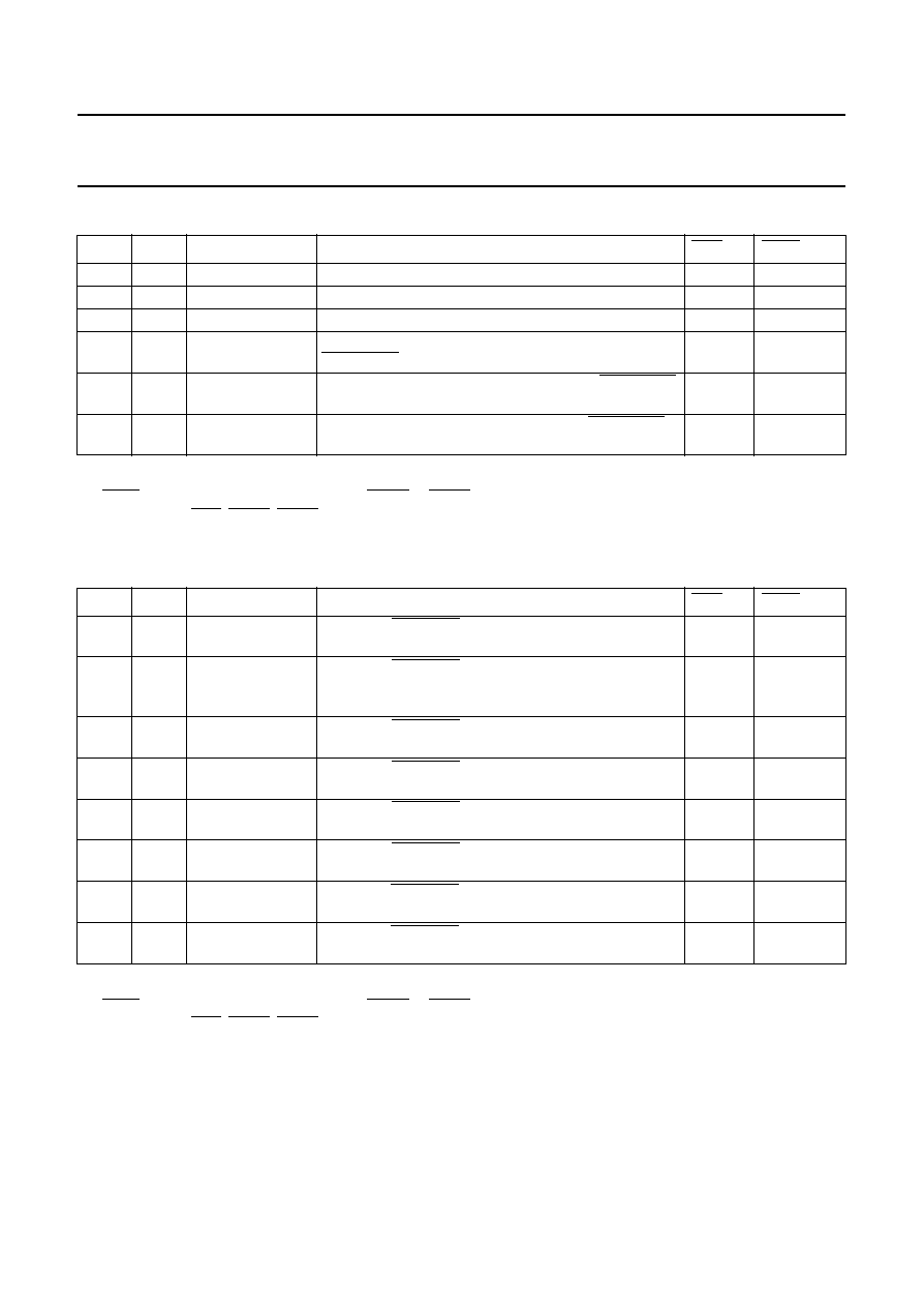
1996 Oct 29
105
Philips Semiconductors
Objective specification
GSM signal processing IC
PCF5083
Table 84 Combined Interrupt Register
Note
1. RSTx = 0 means reset condition if either RSTO or RSTC is asserted; `
-
' denotes not affected from reset line.
During reset (RST, RSTO, RSTC) only those registers with an explicitly given reset value are affected. All other
registers are undefined and have to be set by the controller.
Table 85 High Priority Interrupt Register
Notes
1. RSTx = 0 means reset condition if either RSTO or RSTC is asserted; `
-
' denotes not affected from reset line.
During reset (RST, RSTO, RSTC) only those registers with an explicitly given reset value are affected. All other
registers are undefined and have to be set by the controller.
2. To clear these interrupt flags, the corresponding location has to be written with a logic 1.
BIT
R/W
SYMBOL
OPERATION (if bit is set)
RST = 0
RSTx = 0
(1)
0
R
HWCTRL_INT
HWCTRL_INT interrupt was activated.
-
-
1
R
IOM_INT
IOM_INT interrupt was activated.
-
-
2
R
SI_INT
SI_INT interrupt was activated.
-
-
3
R/W
HWCTRL_MASK
Enable the HWCTRL_INT interrupt to assert the
COMB_INT interrupt line.
0
-
4
R/W
IOM_MASK
Enable the IOM_INT interrupt to assert the COMB_INT
interrupt line.
0
-
5
R/W
SI_MASK
Enable the SI_INT interrupt to assert the COMB_INT
interrupt line.
0
-
BIT
R/W
SYMBOL
OPERATION (if bit is set)
RST = 0
RSTx = 0
(1)
0
R/W
RX_INT
(2)
Assert the HIPR_INT interrupt line when the RX_REG
is sent via the RF Bus.
0
-
1
R/W
RXTX_INT
(2)
Assert the HIPR_INT interrupt line when the TX_REG
is sent via the RF Bus prior to a MON burst in the TX
timeslot.
0
-
2
R/W
TX_INT
(2)
Assert the HIPR_INT interrupt line when the TX_REG
is sent via the RF Bus prior to a TX burst.
0
-
3
R/W
MON_INT
(2)
Assert the HIPR_INT interrupt line when the
MON_REG is sent via the RF Bus.
0
-
4
R/W
AS_INT1
(2)
Assert the HIPR_INT interrupt line when the
DACOFF_REG is sent via the RF Bus.
0
-
5
R/W
FRAME_INT
(2)
Assert the HIPR_INT interrupt line at the beginning of
every TDMA frame.
0
-
6
R
PIRQN_INT
Assert the HIPR_INT interrupt line if the DSP core host
port input request is active.
0
-
7
R
PORQN_INT
Assert the HIPR_INT interrupt line if the DSP core host
port output request is active.
0
-
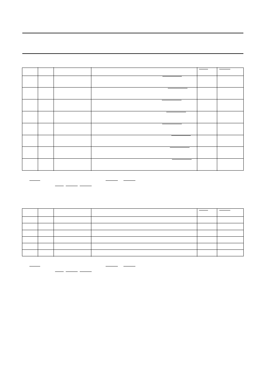
1996 Oct 29
106
Philips Semiconductors
Objective specification
GSM signal processing IC
PCF5083
Table 86 High priority interrupt mask register
Note
1. RSTx = 0 means reset condition if either RSTO or RSTC is asserted; `
-
' denotes not affected from reset line.
During reset (RST, RSTO, RSTC) only those registers with an explicitly given reset value are affected. All other
registers are undefined and have to be set by the controller.
Table 87 Serial Interface Interrupt Register
Note
1. RSTx = 0 means reset condition if either RSTO or RSTC is asserted; `
-
' denotes not affected from reset line.
During reset (RST, RSTO, RSTC) only those registers with an explicitly given reset value are affected. All other
registers are undefined and have to be set by the controller.
BIT
R/W
SYMBOL
OPERATION (if bit is set)
RST = 0
RSTx = 0
(1)
0
R/W
RX_MASK
Enable the RX_INT flag to assert the HIPR_INT
interrupt line.
0
-
1
R/W
RXTX_MASK
Enable the RXTX_INT flag to assert the HIPR_INT
interrupt line.
0
-
2
R/W
TX_MASK
Enable the TX_INT flag to assert the HIPR_INT
interrupt line.
0
-
3
R/W
MON_MASK
Enable the MON_INT flag to assert the HIPR_INT
interrupt line.
0
-
4
R/W
AS_MASK
Enable the AS_INT flag to assert the HIPR_INT
interrupt line.
0
-
5
R/W
FRAME_MASK
Enable the FRAME_INT flag to assert the HIPR_INT
interrupt line.
0
-
6
R/W
PIRQN_MASK
Enable the PIRQN_INT flag to assert the HIPR_INT
interrupt line.
0
-
7
R/W
PORQN_MASK
Enable the PORQN_INT flag to assert the HIPR_INT
interrupt line.
0
-
BIT
R/W
SYMBOL
OPERATION (if bit is set)
RST = 0
RSTx = 0
(1)
0
R
IMC_OBE
RF Bus IMC channel output buffer empty.
0
-
1
R
IMC_IBF
RF Bus IMC channel input buffer full.
0
-
2
R
TXD_OBE
RS232 interface output buffer empty.
0
-
3
R
RXD_IBF
RS232 interface input buffer full.
0
-
4
R
EXT_IOM
External IOM
®
-2 interface request.
0
-
5
R
PAR_ERR
RS232 interface parity error.
0
-
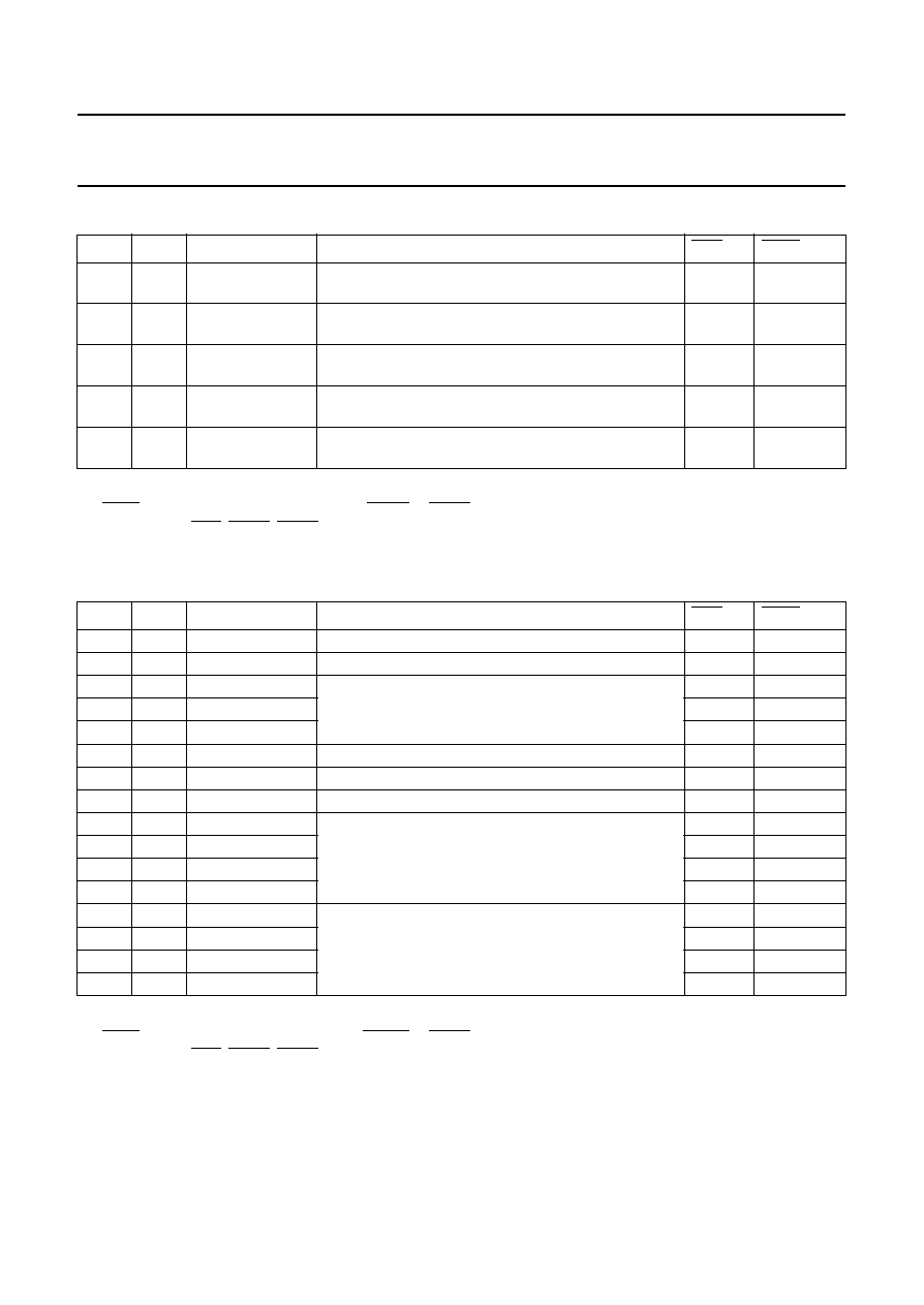
1996 Oct 29
107
Philips Semiconductors
Objective specification
GSM signal processing IC
PCF5083
Table 88 Serial Interface Interrupt Mask Register
Note
1. RSTx = 0 means reset condition if either RSTO or RSTC is asserted; `
-
' denotes not affected from reset line.
During reset (RST, RSTO, RSTC) only those registers with an explicitly given reset value are affected. All other
registers are undefined and have to be set by the controller.
Table 89 IOM
®
-2 Interface Configuration Register
Note
1. RSTx = 0 means reset condition if either RSTO or RSTC is asserted; `
-
' denotes not affected from reset line.
During reset (RST, RSTO, RSTC) only those registers with an explicitly given reset value are affected. All other
registers are undefined and have to be set by the controller.
BIT
R/W
SYMBOL
OPERATION (if bit is set)
RST = 0
RSTx = 0
(1)
0
R/W
IMC_OBE_MASK
Enable the IMC_OBE flag to assert the SI_INT interrupt
condition.
0
-
1
R/W
IMC_IBF_MASK
Enable the IMC_IBF flag to assert the SI_INT interrupt
condition.
0
-
2
R/W
TXD_OBE_MASK Enable the TXD_OBE flag to assert the SI_INT
interrupt condition.
0
-
3
R/W
RXD_IBF_MASK
Enable the RXD_IBF flag to assert the SI_INT interrupt
condition.
0
-
4
R/W
EXT_IOM_MASK
Enable the EXT_IOM flag to assert the SI_INT interrupt
condition.
0
-
BIT
R/W
SYMBOL
OPERATION (if bit is set)
RST = 0
RSTx = 0
(1)
0
R/W
IOMEXT_EN
Set to a logic 1 to enable the external IOM
®
-2 interface
0
-
1
R/W
IOMEXT_INV
Set to a logic 1 to invert the external IOM
®
-2 lines
0
-
2
R/W
CLOCK_MODE0
Select the IOM
®
-2 clock mode
0
-
3
R/W
CLOCK_MODE1
0
-
4
R/W
CLOCK_MODE2
0
-
5
R/W
DATA_MODE
Select the IOM
®
-2 data mode.
0
-
6
R/W
MASTER0_EN
Set to a logic 1 to enable the IOM
®
-2 master unit 0
0
-
7
R/W
MASTER1_EN
Set to a logic 1 to enable the IOM
®
-2 master unit 1
0
-
8
R/W
MASTER0_TS0
Select the IOM
®
-2 timeslot for the IOM
®
-2 master unit 0
0
-
9
R/W
MASTER0_TS1
0
-
10
R/W
MASTER0_TS2
0
-
11
R/W
MASTER0_TS3
0
-
12
R/W
MASTER1_TS0
Select the IOM
®
-2 timeslot for the IOM
®
-2 master unit 1
0
-
13
R/W
MASTER1_TS1
0
-
14
R/W
MASTER1_TS2
0
-
15
R/W
MASTER1_TS3
0
-

1996 Oct 29
108
Philips Semiconductors
Objective specification
GSM signal processing IC
PCF5083
Table 90 Audio Interface Configuration Register
Note
1. RSTx = 0 means reset condition if either RSTO or RSTC is asserted; `
-
' denotes not affected from reset line.
During reset (RST, RSTO, RSTC) only those registers with an explicitly given reset value are affected. All other
registers are undefined and have to be set by the controller.
Table 91 IOM
®
-2 Interface Interrupt Flag Register
Notes
1. RSTx = 0 means reset condition if either RSTO or RSTC is asserted; `
-
' denotes not affected from reset line.
During reset (RST, RSTO, RSTC) only those registers with an explicitly given reset value are affected. All other
registers are undefined and have to be set by the controller.
2. These flags change from `0' to `1' after the IOM
®
-2 interface was enabled with CLOCK_MODE = 0 and
MASTERx_EN = `0' after the state machined of the monitor/CI master units are in an initial state.
BIT
R/W
SYMBOL
OPERATION (if bit is set)
RST = 0
RSTx = 0
(1)
0
R/W
TX_EN
Set to a logic 1 to enable the Voice Port transmit
section
0
-
1
R/W
TX_DEST
Select Voice Port transmit section data port
0
-
2
R/W
RX_EN
Set to a logic 1 to enable the Voice Port receive section
0
-
3
R/W
RX_SOURCE
Select Voice Port receive section data port
0
-
4
R/W
TX_SLOT0
Select IOM
®
-2 timeslot for the Voice Port transmit
section
0
-
5
R/W
TX_SLOT1
0
-
6
R/W
TX_SLOT2
0
-
7
R/W
TX_SLOT3
0
-
8
R/W
RX_SLOT0
Select IOM
®
-2 timeslot for the Voice Port receive
section
0
-
9
R/W
RX_SLOT1
0
-
10
R/W
RX_SLOT2
0
-
11
R/W
RX_SLOT3
0
-
12
R/W
TRANS_EN
Set to a logic 1 to enable the Voice Port transparent
mode
0
-
BIT
R/W
SYMBOL
OPERATION (if bit is set)
RST = 0
RSTx = 0
(1)
0
R
MON0_IBF
Monitor master 0 input buffer full
0
-
1
R
MON0_OBE
(2)
Monitor master 0 output buffer empty
0(1)
-
2
R
MON1_IBF
Monitor master 1 input buffer full
0
-
3
R
MON1_OBE
(2)
Monitor master 1 output buffer empty
0(1)
-
4
R
CI0_IBF
C/I channel master 0 input buffer full
0
-
5
R
CI0_OBE
(2)
C/I channel master 0 output buffer empty
0(1)
-
6
R
CI1_IBF
C/I channel master 1 input buffer full
0
-
7
R
CI1_OBE
(2)
C/I channel master 1 output buffer empty
0(1)
-
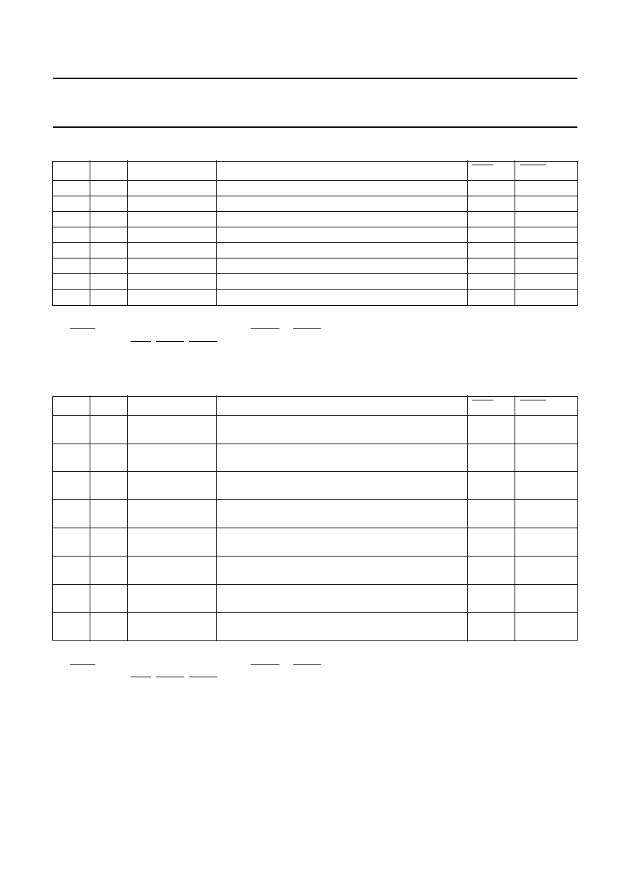
1996 Oct 29
109
Philips Semiconductors
Objective specification
GSM signal processing IC
PCF5083
Table 92 IOM
®
-2 Interface Control Register
Note
1. RSTx = 0 means reset condition if either RSTO or RSTC is asserted; `
-
' denotes not affected from reset line.
During reset (RST, RSTO, RSTC) only those registers with an explicitly given reset value are affected. All other
registers are undefined and have to be set by the controller.
Table 93 IOM
®
-2 Interface Interrupt Enable Register
Note
1. RSTx = 0 means reset condition if either RSTO or RSTC is asserted; `
-
' denotes not affected from reset line.
During reset (RST, RSTO, RSTC) only those registers with an explicitly given reset value are affected. All other
registers are undefined and have to be set by the controller.
BIT
R/W
SYMBOL
OPERATION (if bit is set)
RST = 0
RSTx = 0
(1)
0
R/W
TABORT0
Monitor master 0 transmit abort request
0
-
1
R/W
TABORT1
Monitor master 1 transmit abort request
0
-
2
R
RABORT0
Monitor master 0 receive abort request
0
-
3
R
RABORT1
Monitor master 1 receive abort request
0
-
4
R/W
TEOM0
Monitor master 0 transmit end of message
0
-
5
R/W
TEOM1
Monitor master 1 transmit end of message
0
-
6
R
REOM0
Monitor master 0 receive end of message
0
-
7
R
REOM1
Monitor master 1 receive end of message
0
-
BIT
R/W
SYMBOL
OPERATION (if bit is set)
RST = 0
RSTx = 0
(1)
0
R/W
MON0_IBF_EN
Enable the MON0_IBF flag to assert the IOM_INT
interrupt condition.
0
-
1
R/W
MON0_OBE_EN
Enable the MON0_OBE flag to assert the IOM_INT
interrupt condition.
0
-
2
R/W
MON1_IBF_EN
Enable the MON1_IBF flag to assert the IOM_INT
interrupt condition.
0
-
3
R/W
MON1_OBE_EN
Enable the MON1_OBE flag to assert the IOM_INT
interrupt condition.
0
-
4
R/W
CI0_IBF_EN
Enable the CI0_IBF flag to assert the IOM_INT
interrupt condition.
0
-
5
R/W
CI0_OBE_EN
Enable the CI0_OBE flag to assert the IOM_INT
interrupt condition.
0
-
6
R/W
CI1_IBF_EN
Enable the CI1_IBF flag to assert the IOM_INT
interrupt condition.
0
-
7
R/W
CI1_OBE_EN
Enable the CI1_OBE flag to assert the IOM_INT
interrupt condition.
0
-
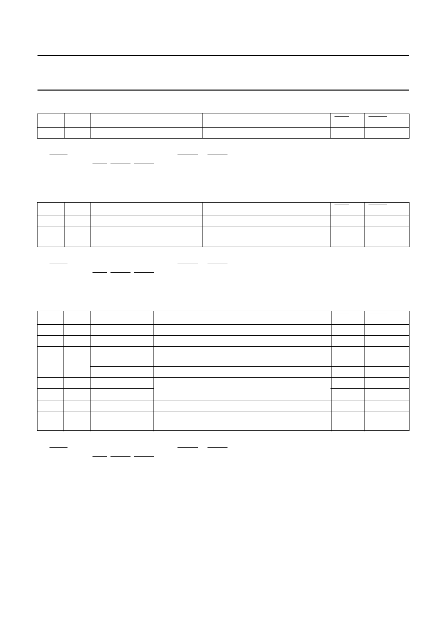
1996 Oct 29
110
Philips Semiconductors
Objective specification
GSM signal processing IC
PCF5083
Table 94 Parallel Port Data Register
Note
1. RSTx = 0 means reset condition if either RSTO or RSTC is asserted; `
-
' denotes not affected from reset line.
During reset (RST, RSTO, RSTC) only those registers with an explicitly given reset value are affected. All other
registers are undefined and have to be set by the controller.
Table 95 Parallel Port Data Direction Register
Note
1. RSTx = 0 means reset condition if either RSTO or RSTC is asserted; `
-
' denotes not affected from reset line.
During reset (RST, RSTO, RSTC) only those registers with an explicitly given reset value are affected. All other
registers are undefined and have to be set by the controller.
Table 96 System Configuration Register (SYSCON)
Note
1. RSTx = 0 means reset condition if either RSTO or RSTC is asserted; `
-
' denotes not affected from reset line.
During reset (RST, RSTO, RSTC) only those registers with an explicitly given reset value are affected. All other
registers are undefined and have to be set by the controller.
BIT
R/W
SYMBOL
OPERATION
RST = 0
RSTx = 0
(1)
0 to 5
R/W
PIO0_DATA to PIO5_DATA
PIO0 to PIO5 input or output data
0
-
BIT
R/W
SYMBOL
OPERATION
RST = 0
RSTx = 0
(1)
0
R
PIO0_DDIR
reserved
0
-
1 to 5
R/W
PIO1_DDIR to PIO5_DDIR
A logic 1 selects the port as an output.
A logic 0 selects the port as an input.
0
-
BIT
R/W
SYMBOL
OPERATION (if bit is set)
RST = 0
RSTx = 0
(1)
0
W
CLK13M
Disable the CLK13M output pin.
0
-
1
W
CLK20M
Disable the CLK20M output pin.
0
-
2
W
CLK32K
Disable the CLK32K output pin; PCF5083-2B and
PCF5083-2C only.
0
-
CLK26M
Disable the CLK26M output pin; PCF5083-3A only.
0
-
3
W
DSP_CLK0
These two bits select the DSP core input clock.
0
-
4
W
DSP_CLK1
0
-
5
W
RS232_CLK
Select the external clock for the RS232 interface
0
-
6
R
LOCK
When a logic 1, the PLL is out of lock. When a logic 0,
the PLL is in lock.
0
-

1996 Oct 29
111
Philips Semiconductors
Objective specification
GSM signal processing IC
PCF5083
10.2
Interrupt Logic
The PCF5083 provides three active LOW interrupt lines:
FRAME_INT, COMB_INT and HIPR_INT for use with the
microcontroller. These interrupt lines are described in
Table 97.
Table 97 Interrupt lines
INTERRUPT
DESCRIPTION
FRAME_INT
This output generates an interrupt at the
beginning of every TDMA frame. The
interrupt is deactivated with an access to
register MODE0_REG.
COMB_INT
This output combines three different
interrupts:
HWCTRL_INT: indicates all interrupts
from the on/off monitor, MMI
power-down unit and the real time clock.
All these interrupt sources are encoded
in register HWCTRL_REG
IOM_INT: indicates all interrupts from
the IOM
®
-2 interface encoded in
registers IOMFLAG_REG and
IOMCTRL_REG. Enable flags for this
interrupt source are provided in register
IOMEN_REG.
SI_INT: indicates all interrupts from the
RF-IC bus interface and the RS232
interface encoded in register
SIINT_REG. Enable flags for this
interrupt source are provided in register
SIMASK_REG.
The register COMBINT_REG contains
an interrupt flag and an enable flag for
each of the three interrupts. The
interrupt flags are inactive if none of their
corresponding interrupt conditions is
active and enabled.
HIPR_INT
This outputs combines some high
priority interrupt sources derived from
the RF-IC bus trigger signals generated
from the timing generator, from the
TDMA frame interrupt and the host port
of the DSP core. The register
HIPRINT_REG holds flags for each
interrupt condition and the register
HIPRMASK_REG the corresponding
interrupt enable flags. For further details
refer to Section 10.1
11 RESET
The PCF5083 has three asynchronous, active LOW reset
inputs: RSTO, RSTC and RST.
RSTO resets the ON/OFF monitor. RSTC the real time
clock unit. For a proper reset, RSTO and RSTC have to be
asserted until the 32.768 kHz oscillator has stabilized.
RST controls all other parts of the PCF5083. RST is
connected to the system reset. For a proper reset, RST
has to be asserted for at least 62.5 ms.
After powering-up the PCF5083 all reset lines RSTO,
RSTC and RST must be asserted to achieve a defined
state of the IC.
The DSP core reset is driven via the general purpose
parallel port bit 0. After an external reset via RST, this port
pin is set to a logic 0. The DSP core is therefore set into
the reset state.
12 JTAG TEST INTERFACE
The PCF5083 JTAG interface is used to increase
testability at board level. The interface is implemented in
accordance with IEEE Std 1149.1-1990, IEEE Standard
Test Access Port and Boundary-Scan Architecture.
The interface signals are specified in Table 98 and the
operations supported by the interface are given in
Table 99.
Table 98 JTAG test interface signals
SIGNAL
DESCRIPTION
TRSTN
Test Reset, active LOW input. This signal
resets the internal TAP controller and the
state of the boundary-scan cells. It must be
pulled LOW during normal operation to
ensure that the boundary scan circuitry does
not influence the application logic.
TCK
Test Clock input.
TMS
Test Mode Select input. This signal controls
the internal state machine of the TAP
controller.
TDI
Test Data Input to shift in instructions and
data are applied to the boundary-scan
circuitry.
TDO
Test Data Out. While shifting in data at the
port TDI, data in also shifted out serially at
this pin. The instruction register and the data
registers are always connected between TDI
and TDO.

1996 Oct 29
112
Philips Semiconductors
Objective specification
GSM signal processing IC
PCF5083
Table 99 Operations supported by the JTAG-circuitry
Notes
1. For all DSP core specific instructions refer to [1].
2. This instruction is always captured in the state Capture_IR of the TAP controller.
3. This instruction is loaded into the instruction register in the state Reset of the TAP-controller.
INSTRUCTION
BINARY CODE
DESCRIPTION OR VALUE
EXTEST
00000
Refer to IEEE standard
ACUTEST
(1)
00001
Test mode for IC production
CONTEST
(1)
00010
Test mode for IC production
DCUTEST
(1)
00011
Test mode for IC production
IOTEST
(1)(1)
00100
Test mode for IC production
FCTTEST
(1)
00101
Test mode for IC production
SFTTEST
(1)
00110
Test mode for IC production
FCTTESTV
(1)
00111
Test mode for IC production
SAMPLE/PRELOAD
01000
Refer to IEEE standard
RESET
(1)
10000
Generate a synchronous reset for the DSP core
GO
(1)
10001
Restart the DSP core at 0x0000 after the RESET instruction
HIGH-Z
10010
Sets all 3-state pins in their high impedance state; TDI, TDO equal to
BYPASS
CLAMP
10011
Pins like EXTEST. TDI, TDO equal to BYPASS
NMI
(1)
10100
Generate a NMI to the DSP core
-
10110
Reserved
-
10111
Reserved
TESTIN
(1)
11000
Select the test input register TI
TESTOUT
(1)
11001
Select the test output register TO
STATUS
11010
Select the status register
IDCODE
(2)
11101
0001 0101110110000110 00000010101 1 (PCF5083-1)
0010 0101110110000110 00000010101 1 (PCF5083-2)
0011 0101110110000110 00000010101 1 (PCF5083-3)
BYPASS
(3)
Others
Refer to IEEE standard
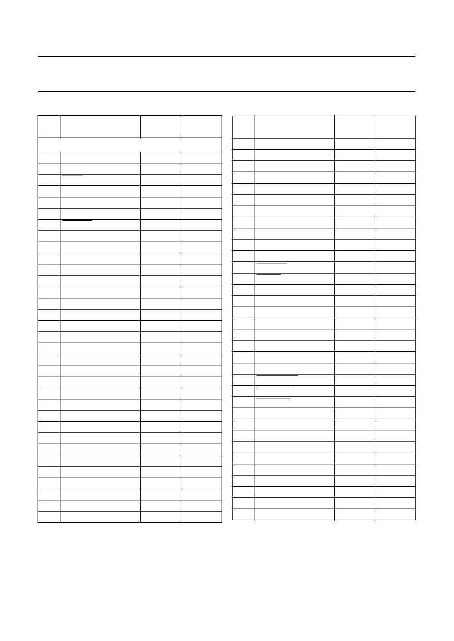
1996 Oct 29
113
Philips Semiconductors
Objective specification
GSM signal processing IC
PCF5083
Table 100 Boundry Scan Chain
NO.
SIGNAL
I/O
3-STATE
CONTROL
TDI
1
REFON
output
105
2
DCLK
input
3
RSTP
input
4
CLKSEL
input
5
CKI
input
6
cki_enable
output
note 1
7
HCEN_T
input
8
IO1
output
9
9
io1_enable
output
10
IO1
input
11
IO2
output
12
12
io2_enable
output
13
IO2
input
14
IO3
output
15
15
io3_enable
output
16
IO3
input
17
IO4
output
18
18
io4_enable
output
19
IO4
input
20
HA0
input
21
HA1
input
22
HA2
input
23
HA3
input
24
HA4
input
25
HA5
input
26
HA6
input
27
hd_enable
output
28
HD0
output
27
29
HD0
input
30
HD1
output
27
31
HD1
input
32
HD2
output
27
33
HD2
input
34
HD3
output
27
35
HD3
input
36
HD4
output
27
37
HD4
input
38
HD5
output
27
39
HD5
input
40
HD6
output
27
41
HD6
input
42
HD7
output
27
43
HD7
input
44
HR/W
input
45
HCEN_D
input
46
DTACK (_enable)
output
46; note 2
47
SIXCLK
input
48
SIXEN
input
49
SIXD
input
50
SOXCLK
input
51
SOXEN
input
52
SOXD
output
53
53
soxd_enable
output
54
CLK20M
output
105
55
FRAME_INT (_enable)
output
55; note 2
56
COMB_INT (_enable)
output
56; note 2
57
HIPR_INT (_enable)
output
57; note 2
58
CLK13M
output
105
59
AFS
input
60
60
afs_enable
output
61
AFS
output
62
ACLK
output
63
63
aclk_enable
output
64
ACLK
input
65
ADI
input
66
ADO
output
103
67
TSCK1
input
NO.
SIGNAL
I/O
3-STATE
CONTROL

1996 Oct 29
114
Philips Semiconductors
Objective specification
GSM signal processing IC
PCF5083
68
TSCK2
input
69
TCE
input
70
PIO1
input
71
PIO1
output
72
77
pio1_enable
output
73
PIO2
input
74
PIO2
output
75
75
pio2_enable
output
76
PIO3
input
77
PIO3
output
78
78
pio3_enable
output
79
PIO4
input
80
PIO4
output
81
81
pio4_enable
output
82
PIO5
input
83
PIO5
output
84
84
pio5_enable
output
85
BEN
output
103
86
TXON
output
103
87
RXON
output
103
88
PDRX1
output
103
89
PDRX2
output
103
90
PDTX1
output
103
91
NPDTX1
output
103
92
NPDTX2
output
103
93
PDBIAS
output
103
94
NPDBIAS
output
103
95
PDSYN
output
103
96
TXKEY1
output
103
97
TXKEY2
output
103
98
DSPEN
input
99
TIMEN
input
100
RSTC
input
101
RSTO
input
102
ONKEY
input
103
gpon1_enable
output
104
CLK32I
input
105
powon_enable
output
NO.
SIGNAL
I/O
3-STATE
CONTROL
Notes
1. H: enable CKI pad to scan cell; L: CKI reads High.
2. Open-drain output.
3. PCF5083-2B and PCF5083-2C versions only.
4. PCF5083-3 only.
106
AUXON
input
107
LOWVOLT
output
108
POWON
output
109
NPOWON
output
110
RST
input
111
CLK32K; note 3
output
105
CLK26M; note 4
112
TXD (_enable)
output
112; note 2
113
RXD
input
114
MMIEN (_enable)
output
114; note 2
115
MMIREQ
input
116
MMICLK
output
105
117
FSC
input
118
FSC
output
119
119
fsc_dcl_enable
output
120
DCL
input
121
DCL
output
119
122
DU
input
123
DD (_enable)
output
123; note 2
124
RFCLK
output
103
125
RFEN1
output
103
126
RFEN2
output
103
127
RFEN3
output
103
128
RFEN4
output
103
129
RFDI
input
130
RFDO
output
103
131
RFE
output
103
132
NREFON
output
105
133
GPON1
output
105
TDO
134
GPON1 (_enable)
output
134; note 2
NO.
SIGNAL
I/O
3-STATE
CONTROL
1996 Oct 29
115
Philips Semiconductors
Objective specification
GSM signal processing IC
PCF5083
13 TEST AND EMULATION MODES
The PCF5083 supports two test and emulation modes which make all internal signals of the DSP or Timer core externally
available. These test modes are selected with either DSPEN = 1 and TIMEN = 0, or DSPEN = 0 and TIMEN = 1.
More information on these test modes will be made available with application notes. Ask your local sales office about the
status of these application notes.
14 LIMITING VALUES
In accordance with the Absolute Maximum Rating System (IEC 134).
Notes
1. Stresses above those listed under Maximum Absolute Ratings may cause permanent damage to the device. This is
a stress rating only and functional operation of the device at these or any other condition above those indicated in
the operation section of this specification is not implied.
2. For operating at elevated temperatures the device must be derated based on 125
°
C maximum junction temperature.
3. This product includes circuitry specifically designed for the protection of its internal devices from the damaging effects
of excessive static charge. Nonetheless, it is suggested that conventional precautions be taken to avoid applying any
voltage larger than the rated maxima.
15 DC CHARACTERISTICS
T
amb
=
-
40 to +85
°
C; V
DD
= 3.3 V
±
10%.
SYMBOL
PARAMETER
MIN.
MAX.
UNIT
V
DD
supply voltage
-
0.5
+5.0
V
V
I
input voltage on any pin with respect to ground (V
SS)
)
-
0.5
V
DD
+ 0.5V
V
I
I
sink current into any pin
-
20
+20
mA
P
tot
total power dissipation
-
800
mW
T
stg
storage temperature
-
65
+150
°
C
T
amb
operating ambient temperature
-
40
+85
°
C
SYMBOL
PARAMETER
(1)
CONDITIONS
MIN.
TYP.
MAX.
UNIT
Supply
V
DD
operating supply voltage
2.7
3.0
3.6
V
I
DD
operating supply current
all sections operating;
Timer active, DSP encoding
speech; note 2
I
(VDD2)
+ I
(VDDPLL)
-
40
50
mA
I
(VDD1)
note 3
-
8
-
mA
I
DDtot
I
(VDD2)
+ I
(VDDPLL)
+ I
(VDD1)
-
48
-
mA
I
DD(SLP)
supply current Sleep mode
Timer sleeping, DSP
inactive
I
(VDD2)
+ I
(VDDPLL)
-
250
500
µ
A
I
(VDD1)
note 3
-
340
-
µ
A
I
DD(SLP)tot
I
(VDD2)
+ I
(VDDPLL)
+ I
(VDD1)
-
590
-
µ
A

1996 Oct 29
116
Philips Semiconductors
Objective specification
GSM signal processing IC
PCF5083
Notes
1. V
DD1
= pad ring power supply; V
DD2
= core power supply and V
DDPLL
= analog PLL power supply.
2. Current consumption during active speech encoding is measured and then derated by 0.8 to reflect activity level
during one cycle.
3. I
DD1
is estimated with a 30 pF load on each output.
I
DD(STBY)
supply current Standby mode
ON/OFF logic and RTC
active
I
(VDD2)
+ I
(VDDPLL)
-
15
100
µ
A
I
(VDD1)
note 3
-
245
-
µ
A
I
DD(STBY)tot
I
(VDD2)
+ I
(VDDPLL)
+ I
(VDD1)
-
260
-
µ
A
All inputs except CK32I, CKI and Schmitt trigger inputs
V
IL
LOW level input voltage
-
-
0.3V
DD
V
V
IH
HIGH level input voltage
0.7V
DD
-
V
DD
V
I
IL
LOW level sink current
without pull-down resistor
V
IN
= 0
-
-
1
µ
A
I
IH
HIGH level source current
with pull-down resistor
V
IN
= V
DD
40
150
250
µ
A
I
ZL
3-state output leakage current
V
O
= 0 to V
DD
-
-
1
µ
A
All outputs
V
OL
LOW level output voltage
-
-
0.4
V
V
OH
HIGH level output voltage
(except open-drain outputs)
0.8V
DD
-
-
V
I
LI
open-drain output leakage
current
V
O
= 0 to V
DD
-
-
1
µ
A
CMOS Schmitt trigger inputs
V
IL
LOW level input voltage
0
-
0.25V
DD
V
V
IH
HIGH level input voltage
0.75V
DD
-
V
DD
V
V
HYS
Hysteresis
-
0.7
-
V
CK32I
I
IL
LOW level sink current
V
IN
= 0; CK32O open
-
-
1
µ
A
I
IH
HIGH level source current
V
IN
= V
DD
; CK32O open
-
-
1
µ
A
C
in
input capacitance
-
20
-
pF
g
m
32 kHz oscillator
transconductance
CK32I = CK32O = 0.6V
DD
5
-
25
µ
S
CKI
V
IN
input voltage swing
DC bias = 0.35V
DD
(internally generated)
0.7
-
V
DD
-
V
SS
V
SYMBOL
PARAMETER
(1)
CONDITIONS
MIN.
TYP.
MAX.
UNIT

1996 Oct 29
117
Philips Semiconductors
Objective specification
GSM signal processing IC
PCF5083
16 AC CHARACTERISTICS
T
amb
=
-
40 to +85
°
C; V
DD
= 3.3 V
±
10%; see notes 1 to 4.
NO
PARAMETER
MIN.
TYP.
MAX.
UNIT
13 MHz clock timing (see Figs 22 and 24; note 5)
1
CKI HIGH time
20
-
-
ns
2
CKI LOW time
20
-
-
ns
3
CKI frequency (1/t
13
)
-
13
-
MHz
4
CLK13M HIGH to CKI HIGH delay
-
30
-
ns
5
CLK13M LOW to CKI LOW delay
-
30
-
ns
6
MMICLK HIGH to CKI HIGH delay
-
30
-
ns
7
MMICLK LOW to CKI LOW delay
-
30
-
ns
-
PLL lock time with respect to RSTP HIGH
-
-
50
µ
s
32 kHz clock timing (see Figs 25 and 26; note 6)
3
CLK32K frequency
-
32.768
-
kHz
26 MHz clock timing (see Fig.23; notes 5 and 7)
1
CLK26M HIGH time
5
-
-
ns
2
CLK26M LOW time
5
-
-
ns
3
CLK26M frequency
-
26
-
MHz
DSP and RS232 clock timing (see Figs 27 and 28; note 6)
1
DCLK frequency; note 8
-
-
39
MHz
2
DCLK HIGH time
10
-
-
ns
3
DCLK LOW time
10
-
-
ns
4
External RS232 Interface clock frequency -
19200 Baud (provided via ADI and selected with
SYSCON_REG[RS232_CLK] = 1)
-
11.0592
-
MHz
5
External RS232 Interface clock HIGH time
-
90.4
-
ns
6
External RS232 Interface clock LOW time
-
90.4
-
ns
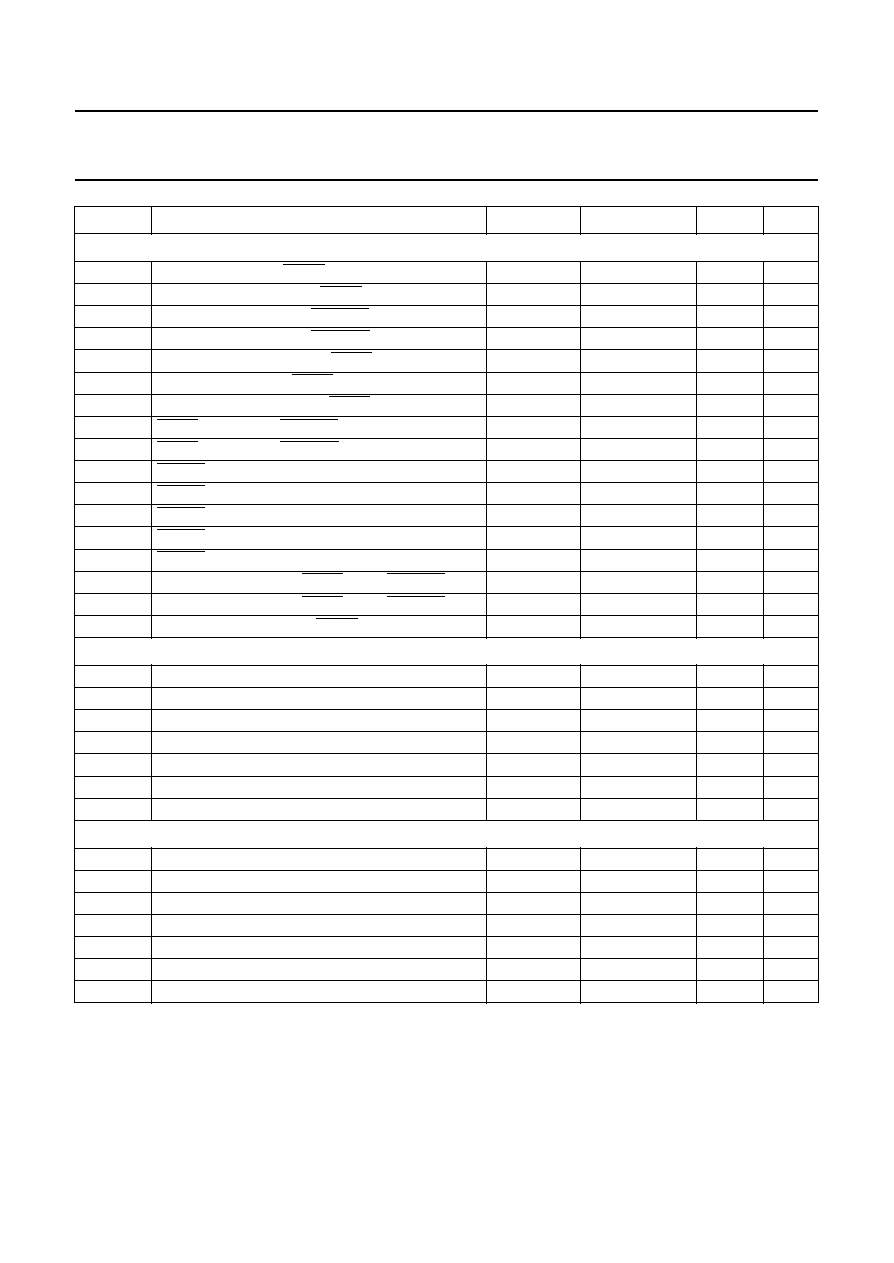
1996 Oct 29
118
Philips Semiconductors
Objective specification
GSM signal processing IC
PCF5083
Host Interface timing (see Figs 29 and 30)
1
HR/W setup time to HCEN LOW
5
-
-
ns
2
HA0 to HA6 setup time to HCEN LOW
5
-
-
ns
3a
HD0 to HD7 setup time (HCEN_T)
t
13
-
-
ns
3b
HD0 to HD7 setup time (HCEN_D)
10
-
-
ns
4
HD0 to HD7 hold time after HCEN HIGH
10
-
-
ns
5
HR/W hold time after HCEN HIGH
5
-
-
ns
6
HA0 to HA6 hold time after HCEN HIGH
10
-
-
ns
7a
HCEN pulse width (HCEN_T)
3t
13
-
-
ns
7b
HCEN pulse width (HCEN_D)
2t
dclkout
+ 20
-
-
ns
8
(9)
DTACK LOW delay time, DSP write cycle
-
30
-
ns
9
DTACK HIGH delay time, DSP read cycle; note 3
-
40
-
ns
10
(10)
DTACK LOW delay time, DSP read cycle
-
30
-
ns
11
DTACK LOW to data valid; note 11
-
35
50
ns
12
DTACK HIGH delay time, DSP read cycle; note 3
-
40
-
ns
13a
HD0 to HD7 valid after HCEN LOW (HCEN_T)
-
-
3t
13
ns
13b
HD0 to HD7 valid after HCEN LOW (HCEN_T)
-
-
45
ns
14
HD0 to HD7 3-state after HCEN HIGH
-
-
30
ns
RF Device Control Bus timing - Mode 0 (see Fig.31; note 12)
1
RFEN1 to RFEN4 setup time to RFCLK LOW
-
4t
13
-
ns
2
RFEN1 to RFEN4 hold time after RFCLK HIGH
-
2t
13
-
ns
3
RFCLK HIGH time
-
6t
13
-
ns
4
RFCLK LOW time
-
6t
13
-
ns
5
RFDO setup time to RFCLK HIGH
-
10t
13
-
ns
6
RFDO hold time after RFCLK HIGH
-
2t
13
-
ns
7
(7)
RFDI setup time to RFCLK HIGH
70
-
-
ns
RF Device Control Bus timing - Mode 1 (see Fig.32; note 12)
1
RFEN1 to RFEN4 setup time to RFCLK HIGH
-
4t
13
-
ns
2
RFEN1 to RFEN4 hold time after RFCLK LOW
-
2t
13
-
ns
3
RFCLK LOW time
-
6t
13
-
ns
4
RFCLK HIGH time
-
6t
13
-
ns
5
RFDO setup time to RFCLK HIGH
-
4t
13
-
ns
6
RFDO hold time after RFCLK LOW
-
2t
13
-
ns
7
(7)
RFDI setup time to RFCLK LOW
70
-
-
ns
NO
PARAMETER
MIN.
TYP.
MAX.
UNIT

1996 Oct 29
119
Philips Semiconductors
Objective specification
GSM signal processing IC
PCF5083
RF Device Control Bus timing - Mode 2 (see Fig.33; note 12)
1
RFEN1 to RFEN4 setup time to RFCLK HIGH
-
4t
13
-
ns
2
RFEN1 to RFEN4 hold time after RFCLK LOW
-
14t
13
-
ns
3
RFCLK LOW time
-
6t
13
-
ns
4
RFCLK HIGH time
-
6t
13
-
ns
5
RFDO setup time to RFCLK HIGH
-
4t
13
-
ns
6
RFDO hold time after RFCLK LOW
-
2t
13
-
ns
7
(7)
RFDI setup time to RFCLK LOW
70
-
-
ns
8
RFE setup time to RFEN1 to RFEN4 LOW
-
6t
13
-
ns
Baseband Interface timing (DSP Core X_Port) (see Fig.34)
1
SIXEN setup to SIXCLK HIGH
5
-
-
ns
2
SIXD setup to SIXCLK HIGH
5
-
-
ns
3
SIXD hold time after SIXCLK HIGH
10
-
-
ns
4
SIXEN hold time after SIXCLK HIGH
10
-
-
ns
5
SIXCLK frequency
-
13
-
MHz
6
SIXCLK LOW time
20
-
-
ns
7
SIXCLK HIGH time
20
-
-
ns
8
SOXEN setup time to SOXCLK LOW
20
-
-
ns
10
SOXD hold time after SOXCLK LOW
-
-
40
ns
11
SOXEN hold time after SOXCLK LOW
10
-
-
ns
12
SOXD 3-state after SOXEN HIGH
-
-
20
ns
13
SOXCLK frequency
-
0.27
13
MHz
14
SOXCLK LOW time
20
1800
-
ns
15
SOXCLK HIGH time
20
1800
-
ns
IOM -2 Interface timing (see Figs 35 and 36)
1
(7)
DD hold time after DCL HIGH
-
30
-
30
ns
2a
(13)
DCL cycle time
-
8.5t
13
-
ns
2b
(13)
DCL cycle time
-
8t
13
-
ns
2c
(13)
DCL frequency
-
4.096
-
MHz
3
(7)
FSC hold time after DCL HIGH
-
30
-
30
ns
4
(7)
DU setup time to DCL LOW
50
-
-
ns
5
(7)
DU hold time after DCL LOW
50
-
-
ns
6
(13)(7)
DCL HIGH time
75
-
-
ns
7
(13)(7)
DCL LOW time
75
-
-
ns
NO
PARAMETER
MIN.
TYP.
MAX.
UNIT

1996 Oct 29
120
Philips Semiconductors
Objective specification
GSM signal processing IC
PCF5083
Voice Port timing - non-transparent mode (see Fig.37 and note 14)
1
(7)
AFS setup time to ACLK HIGH
200
-
-
ns
2
(7)
AFS hold time after ACLK LOW
10
-
-
ns
3
(7)
ADO hold time after ACLK HIGH
-
30
ns
4
(7)
ADI setup time to ACLK LOW
30
-
-
ns
5
(7)
ADI hold time to ACLK LOW
40
-
-
ns
6
(7)
ACLK frequency
-
-
1
MHz
7
(7)
ACLK HIGH time
400
-
-
ns
8
(7)
ACLK LOW time
400
-
-
ns
JTAG Port timing (see Fig.38)
1
TCK LOW time
35
-
-
ns
2
TCK HIGH time
25
-
-
ns
3
TCK cycle time
-
-
10
ns
4
TMS setup time to TCK HIGH
10
-
-
ns
5
TMS hold time after TCK HIGH
30
-
-
ns
6
TDI setup time to TCK HIGH
5
-
-
ns
7
TDI hold time after TCK HIGH
30
-
-
ns
8
TDO asserted after TCK LOW
-
-
60
ns
9
TDO hold time after TCK LOW
-
-
60
ns
10
TDO 3-state after TCK LOW
-
-
30
ns
11
TRSTN pulse width
100
-
-
ns
General purpose parallel port (see Fig.39)
1
PIO data valid after CLK13M rising edge (output)
-
70
-
ns
2
PIO data setup time
-
10
-
ns
3
PIO data valid after CLK13M rising edge (input)
-
70
-
ns
All outputs
t
r
(7)
rise time
-
-
20
ns
t
f
(7)
fall time
-
-
20
ns
NO
PARAMETER
MIN.
TYP.
MAX.
UNIT

1996 Oct 29
121
Philips Semiconductors
Objective specification
GSM signal processing IC
PCF5083
Notes to the AC characteristics
1. Parameters are valid over the specified temperature range.
2. All voltages are measured with respect to ground (V
SS
). For testing all inputs swing between 0 V and V
DD
with a
transition time of 4 ns. All time measurements are made with input voltages of 0 V and V
DD
and output voltages of
0.2
VDD
and 0.8V
DD
as appropriate.
3. Test conditions for outputs: C
L
= 40 pF, except open-drain outputs. Test conditions for open-drain outputs:
C
L
= 40 pF; I
L
= 1.8 mA at V
DD
.
4. All timing diagrams should only be referred to in regard to the edge-to-edge measurements of the timing
specifications. They are not intended as a functional description of the input and output signals. Refer to the
functional description and related timing diagrams for device operation. All setup and hold times are specified with
respect to V
IH
and V
IL
. All delay times with respect to 0.5V
DD
. Times with only typical values are not tested during IC
production
5. For testing the AC characteristics, the low swing input CKI is driven with a square wave signal of the specified
minimum peak-to-peak input voltage swing. The typical values for additional components are: C1 = 4.7 nF,
C
2
= 100 pF and R
1
= 10 k
.
6. For testing the AC characteristics, the input CLK32I is driven with a standard test signal (see note 2). A typical
application for crystal operation is: R = 10 M
, fQ = 32.768 kHz, C
1
= 15 pF, C
T
= 15 pF (for crystal C
L
= 12.5 pF).
7. These times are guaranteed by design and are not tested during IC production.
8. DCLK internally divided-by-two to drive the DSP; t
DCLKOUT
=
1
/
DCLK.
9. This time specified is when PI is empty.
10. This time specified is when PO is full.
11. Not tested in production.
12. Mode 0 and 1, or Mode 2 are selected by register settings. Refer to the functional specification.
13. The output DCL has two different cycle times depending on the DCL period number. Refer to the functional
description. The table lists the cycle times for the 1.536 MHz internal clock mode and the maximum clock frequency
in external clock mode. The minimum cycle times correspond to the 4.096 MHz external clock mode and therefore
apply to all the external clock modes.
14. The Audio Interface timing is given for the non-transparent mode. In transparent mode the IOM
®
-2 Interface timing
applies to the Audio Interface accordingly, refer to functional description.
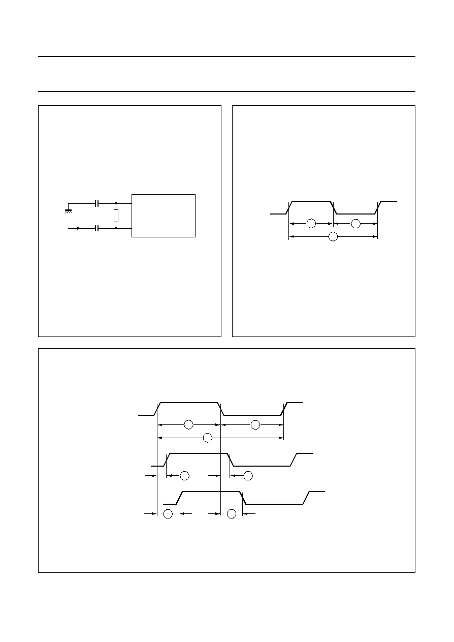
1996 Oct 29
122
Philips Semiconductors
Objective specification
GSM signal processing IC
PCF5083
Fig.22 13 MHz Clock circuit.
handbook, halfpage
MGE300
CKO
CKI
VI
C1
C2
R1
Fig.23 CLK26M Clock timing.
handbook, halfpage
MGD704
CLK26M
3
1
2
Fig.24 13 MHz Clock timing.
handbook, full pagewidth
MGE301
CKI
CLK13M
MMICLK
3
1
4
5
6
7
2
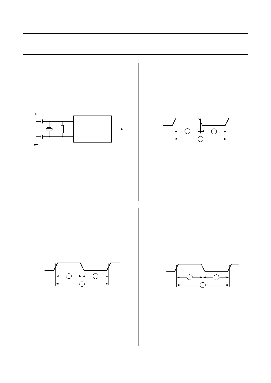
1996 Oct 29
123
Philips Semiconductors
Objective specification
GSM signal processing IC
PCF5083
Fig.25 32.768 kHz Clock circuit.
handbook, halfpage
MGE302
CLK32K
CLK32I
CLK32O
R
(3)
Q
(2)
CL
(1)
CL
(1)
Fig.26 32.768 kHz Clock timing.
handbook, halfpage
MGE303
CLK32K
3
1
2
Fig.27 DSP Clock timing.
handbook, halfpage
MGE304
DCLK
1
2
3
Fig.28 RS232 Clock timing.
handbook, halfpage
MGE305
external RS232
interface clock
(via ADI)
4
5
6
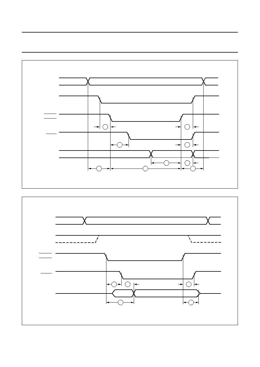
1996 Oct 29
124
Philips Semiconductors
Objective specification
GSM signal processing IC
PCF5083
Fig.29 Host Interface Write timing.
handbook, full pagewidth
MGE315
HA0 to HA6
HR/W
HCEN_T
HCEN_D
DTACK
HD0 to HD7
1
5
9
8
3
7
4
6
2
Fig.30 Host Interface Read timing.
handbook, full pagewidth
MGE316
HA0 to HA6
HR/W
HCEN_T
HCEN_D
HD0 to HD7
12
14
13
10
11
DTACK
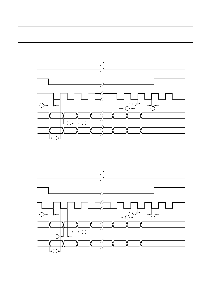
1996 Oct 29
125
Philips Semiconductors
Objective specification
GSM signal processing IC
PCF5083
Fig.31 RF-IC Control Bus timing
-
Mode 0.
handbook, full pagewidth
MGE306
2
1
5
7
6
4
RFE
RFEN1
to
RFEN4
RFCLK
RFDO
D16
D15
D14
A2
A1
A0
D20
D19
D18
D2
D1
D0
RFDI
3
Fig.32 RF-IC Control Bus timing
-
Mode 1.
3
2
4
handbook, full pagewidth
MGE307
5
7
6
RFE
RFEN1
to
RFEN4
RFCLK
RFDO
D16
D15
D14
A2
A1
A0
D20
D19
D18
D2
D1
D0
RFDI
1
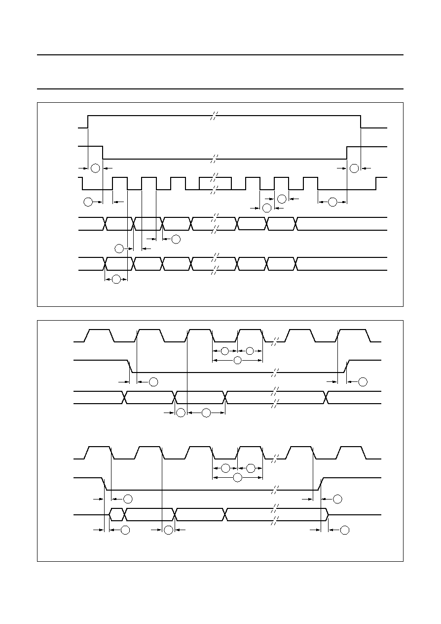
1996 Oct 29
126
Philips Semiconductors
Objective specification
GSM signal processing IC
PCF5083
Fig.33 RF-IC Control Bus timing
-
Mode 2.
handbook, full pagewidth
MGE308
2
3
8
9
1
5
7
6
4
RFE
RFEN1
to
RFEN4
RFCLK
RFDO
D15
D14
D13
D2
D1
D0
D15
D14
D13
D2
D1
D0
RFDI
Fig.34 Baseband Interface timing (DSP Core x-Port).
handbook, full pagewidth
MGE309
6
5
7
SIXCLK
SIXEN
SIXD
SOXCLK
SOXEN
SOXD
8
9
10
14
13
15
12
11
4
1
2
3
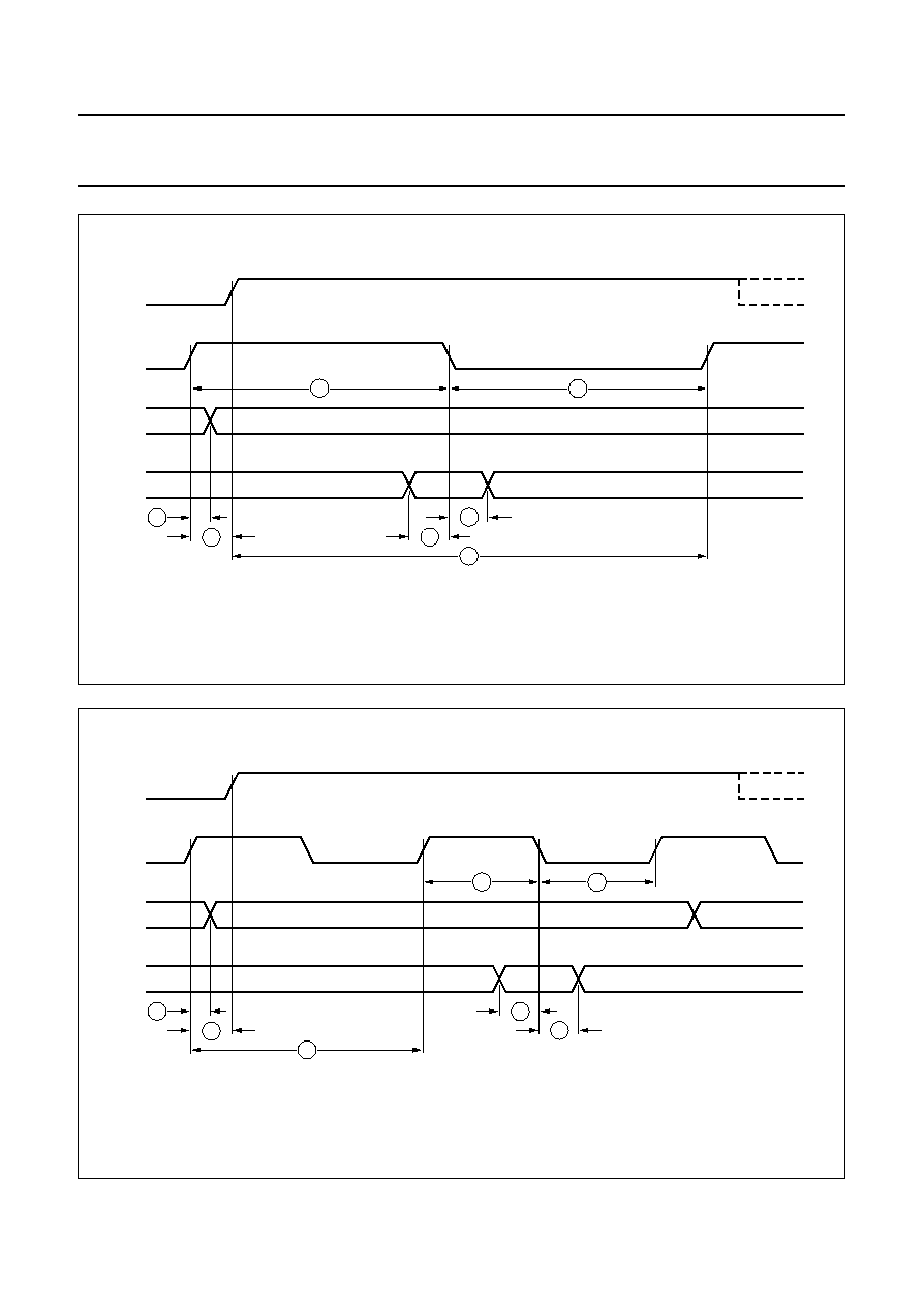
1996 Oct 29
127
Philips Semiconductors
Objective specification
GSM signal processing IC
PCF5083
handbook, full pagewidth
MGE311
DU
DD
DCL
FSC
1
3
2
4
6
7
5
Fig.35 IOM
®
-2 Interface timing - Single Clock cycle mode.
handbook, full pagewidth
MGE310
DU
DD
DCL
FSC
1
3
2
4
6
7
5
Fig.36 IOM
®
-2 Interface timing - Double Clock cycle mode.
1996 Oct 29
128
Philips Semiconductors
Objective specification
GSM signal processing IC
PCF5083
Fig.37 Audio Interface timing (non-transparent mode).
handbook, full pagewidth
MGE312
8
6
7
5
4
3
1
2
ACLK
AFS
ADO
ADI
Fig.38 JTAG port timing.
handbook, full pagewidth
MGE313
TCK
TMS
TDI
TDO
TRSTN
6
4
5
7
1
2
3
11
10
9
8
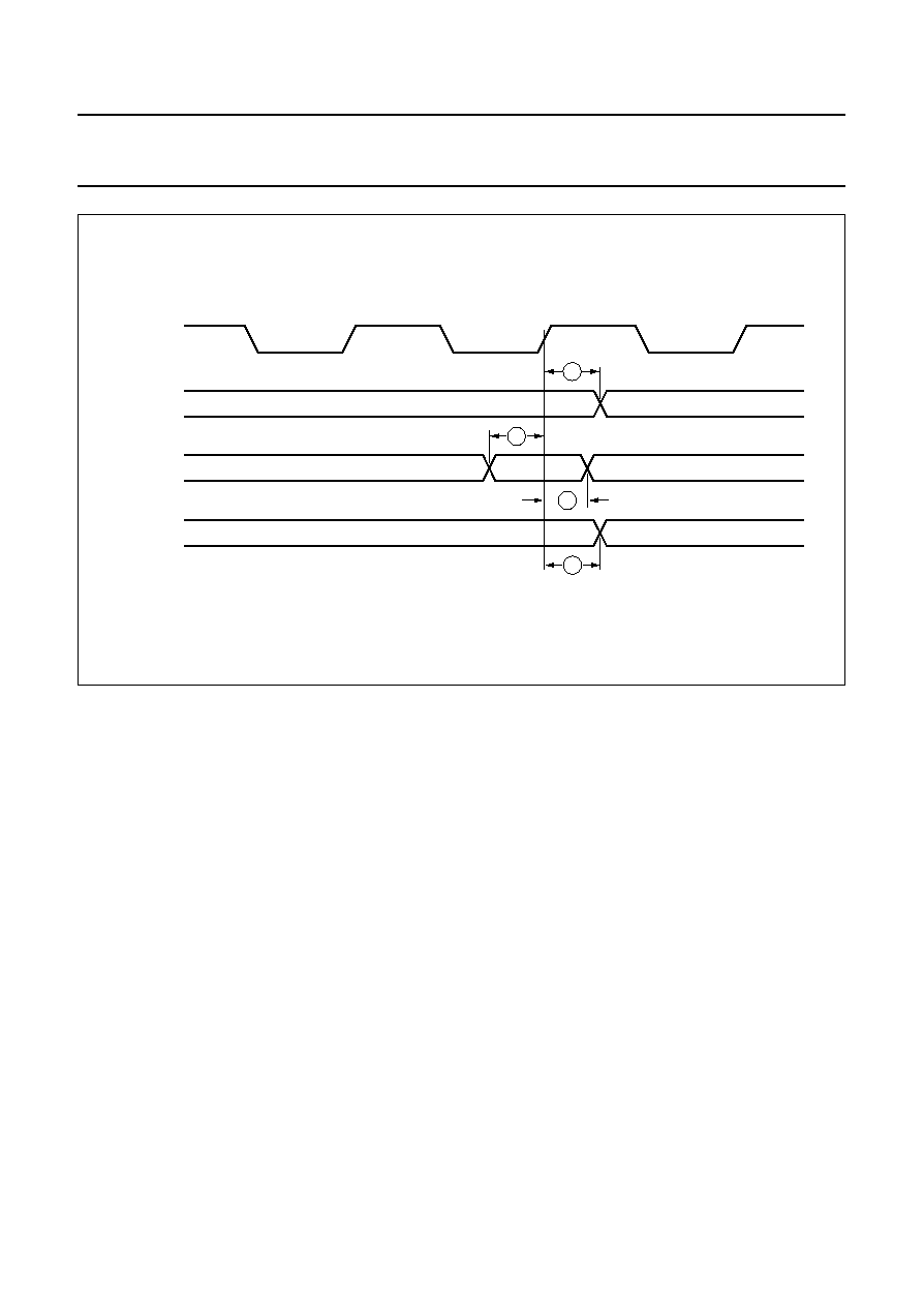
1996 Oct 29
129
Philips Semiconductors
Objective specification
GSM signal processing IC
PCF5083
Fig.39 General purpose parallel port.
handbook, full pagewidth
MGE314
CLK13M
PI01 to PI05
(OUTPUT)
PI01 to PI05
(INPUT)
PI01 to PI05
(DIRECTION)
5
3
2
1
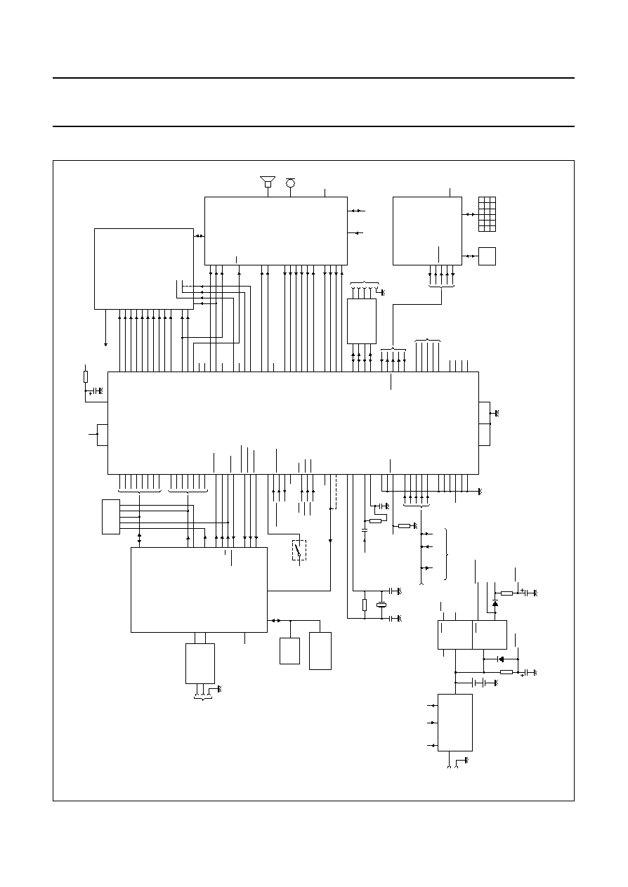
1996 Oct 29
130
Philips Semiconductors
Objective specification
GSM signal processing IC
PCF5083
17 APPLICATION INFORMATION
handbook, full pagewidth
1
µ
F
95
96
97
98
101
102
103
104
HD0
HD1
HD2
HD3
HD4
HD5
HD6
HD7
HA0
HA1
HA2
HA3
HA4
HA5
HA6
ONKEY
AUXON
POWON
AUXON
POWON
NPOWON
CLK32K
CLK13M
CLK20M
DCLK
CLKSEL
TCK
TMS
TDI
TDO
TRSTN
TCKIO
TCE
TSCK1
TSCK2
DSPEN
TIMEN
CLK32I
CLK32O
CKI
CKO
HCEN_T
HCEN_D
HR/W
88
89
90
91
92
93
94
83
106
105
107
32
33
34
35
36
82
75
76
77
79
78
1
127
128
24
25
37
27
26
38
120
116
66
68
67
30
29
73
70
117
118
119
12
13
14
15
18
19
20
21
22
23
52
53
54
55
56
60
59
DO
DI
SCLK
RXON
TXON
BOCLK
BOEN
BDO
BICLK
BIEN
BDI
AFS
control
system
functions
ACLK
ADO
digital
voice and data
interface
ADI
TXD
RXD
XTAL1
MMIREQ
61
63
64
8
9
7
108
109
110
42
2
3
4
6
5
84
85
86
87
111
114
115
123
124
125
126
40
39
41
43
45
44
46
47
65
62
DTACK
FRAME_INT
COMB_INT
HIPR_INT
LOWVOLT
LOWVOLT
RST
PDRX1
PDRX2
PDTX1
NPDTX1
NPDTX2
PDBIAS
NPDBIAS
PDSYN
TXKEY1
TXKEY2
CSxN
D0 to D7
A7 to Ax
A0 to A6
CS0N
CS1N
INT4N
INT5N
INT6N
XTAL1
ON/OFF
key
4.7 nF
10 M
32768 Hz
100
pF
SDA,
SCL
RFCLK
RFEN1
RFEN2
RFEN3
RFEN4
RFDI
TXON
RXON
BEN
SIXCLK
SIXEN
SIXD
SOXCLK
SOXEN
SOXD
AFS
ACLK
ADI
ADO
RXD
TXD
MMICLK
MMIREQ
PIO4
PIO1
PIO2
PIO3
PIO5
PIO4
PIO1
PIO2
PIO3
PIO5
IO1/AEN
IO2
IO3/IRQN
IO4/DTX
DCL
FSC
DU
DD
RFDO
RFE
GPON1
GPON2
REFON
NREFON
RSTO
RSTC
RST
RSTO
RSTC
RSTP
MMIEN
V
DD1
V
DD
V
DD3
V
DD2
V
SS1
V
SS2
V
SSPLL
V
DD1
TXD
RXD
V
DD1
V
DD1
V
DD2
V
DD2
V
DDPLL
100 k
power on/off
13 MHz on/off
RF-UNIT
CONTROLLER
90CL301
PCF5083
I/Q, DAC's
AUXADC's
MMI CONTROLLER
JTAG
PCF5072
TDA8005
MGE318
BASEBAND
INTERFACE
SA1620
SA1638
PCF5075
UMA1019
.
.
.
V
DD1
V
DD
DRIVER,
EMV
+
ESD
PROTECTION
MMIEN
SIM
KEYBOARD
DRIVER,
EMV
+
ESD
PROTECTION
RS232
fax and data
interface
DISPLAY
I
2
C
EEPROM
13 MHz
reference clock
1 V
pp
REFON
JTAG
test-
connector
TMS, TCK
TRSTN
TDO
other ICs
TDI
15
pF
15
pF
100
k
100
k
PIOx
AUXON
LOWVOLT
RSTC
V
DD1
V
DD3
V
DD2
3.3 V
3.3 V
PCY5072
AUXADC's
CHARGING
CIRCUITRY
control
battery
(4 cells)
charger
plugged in
charger
supply
ON
IN
IN
RST
POWON
RSTO
OUT
OUT
RES
PFO
47000
µ
F
GoldCap
3.3
µ
F
1 M
100
k
RAM/ROM
R/W
DTACK
EN
reference clock
13 MHz
Fig.40 Application diagram.
1996 Oct 29
131
Philips Semiconductors
Objective specification
GSM signal processing IC
PCF5083
18 PACKAGE OUTLINE
UNIT
A
1
A
2
A
3
b
p
c
E
(1)
e
H
E
L
L
p
Q
Z
y
w
v
REFERENCES
OUTLINE
VERSION
EUROPEAN
PROJECTION
ISSUE DATE
IEC
JEDEC
EIAJ
mm
0.15
0.05
1.45
1.35
0.25
0.23
0.13
0.20
0.09
14.1
13.9
0.4
16.15
15.85
0.70
0.58
0.95
0.65
7
0
o
o
0.08
0.2
0.1
1.0
DIMENSIONS (mm are the original dimensions)
Note
1. Plastic or metal protrusions of 0.25 mm maximum per side are not included.
0.75
0.45
SOT420-1
96-02-07
D
(1)
(1)
(1)
14.1
13.9
H
D
16.15
15.85
E
Z
0.95
0.65
D
0
5
10 mm
scale
b
p
e
E
A
1
A
L
p
Q
detail X
L
(A )
3
B
c
b
p
E
H
A
2
D
H
v
M
B
D
Z D
A
Z E
e
v
M
A
X
y
w
M
w
M
A
max.
1.6
LQFP128: plastic low profile quad flat package; 128 leads; body 14 x 14 x 1.4 mm
SOT420-1
96
97
pin 1 index
65
64
33
32
1
128

1996 Oct 29
132
Philips Semiconductors
Objective specification
GSM signal processing IC
PCF5083
19 SOLDERING
19.1
Introduction
There is no soldering method that is ideal for all IC
packages. Wave soldering is often preferred when
through-hole and surface mounted components are mixed
on one printed-circuit board. However, wave soldering is
not always suitable for surface mounted ICs, or for
printed-circuits with high population densities. In these
situations reflow soldering is often used.
This text gives a very brief insight to a complex technology.
A more in-depth account of soldering ICs can be found in
our
"IC Package Databook" (order code 9398 652 90011).
19.2
Reflow soldering
Reflow soldering techniques are suitable for all LQFP
packages.
Reflow soldering requires solder paste (a suspension of
fine solder particles, flux and binding agent) to be applied
to the printed-circuit board by screen printing, stencilling or
pressure-syringe dispensing before package placement.
Several techniques exist for reflowing; for example,
thermal conduction by heated belt. Dwell times vary
between 50 and 300 seconds depending on heating
method. Typical reflow temperatures range from
215 to 250
°
C.
Preheating is necessary to dry the paste and evaporate
the binding agent. Preheating duration: 45 minutes at
45
°
C.
19.3
Wave soldering
Wave soldering is not recommended for LQFP packages.
This is because of the likelihood of solder bridging due to
closely-spaced leads and the possibility of incomplete
solder penetration in multi-lead devices.
If wave soldering cannot be avoided, the following
conditions must be observed:
·
A double-wave (a turbulent wave with high upward
pressure followed by a smooth laminar wave)
soldering technique should be used.
·
The footprint must be at an angle of 45
°
to the board
direction and must incorporate solder thieves
downstream and at the side corners.
Even with these conditions, do not consider wave
soldering LQFP packages LQFP48 (SOT313-2),
LQFP64 (SOT314-2) or LQFP80 (SOT315-1).
During placement and before soldering, the package must
be fixed with a droplet of adhesive. The adhesive can be
applied by screen printing, pin transfer or syringe
dispensing. The package can be soldered after the
adhesive is cured.
Maximum permissible solder temperature is 260
°
C, and
maximum duration of package immersion in solder is
10 seconds, if cooled to less than 150
°
C within
6 seconds. Typical dwell time is 4 seconds at 250
°
C.
A mildly-activated flux will eliminate the need for removal
of corrosive residues in most applications.
19.4
Repairing soldered joints
Fix the component by first soldering two diagonally-
opposite end leads. Use only a low voltage soldering iron
(less than 24 V) applied to the flat part of the lead. Contact
time must be limited to 10 seconds at up to 300
°
C. When
using a dedicated tool, all other leads can be soldered in
one operation within 2 to 5 seconds between
270 and 320
°
C.

1996 Oct 29
133
Philips Semiconductors
Objective specification
GSM signal processing IC
PCF5083
20 DEFINITIONS
21 LIFE SUPPORT APPLICATIONS
These products are not designed for use in life support appliances, devices, or systems where malfunction of these
products can reasonably be expected to result in personal injury. Philips customers using or selling these products for
use in such applications do so at their own risk and agree to fully indemnify Philips for any damages resulting from such
improper use or sale.
Data sheet status
Objective specification
This data sheet contains target or goal specifications for product development.
Preliminary specification
This data sheet contains preliminary data; supplementary data may be published later.
Product specification
This data sheet contains final product specifications.
Limiting values
Limiting values given are in accordance with the Absolute Maximum Rating System (IEC 134). Stress above one or
more of the limiting values may cause permanent damage to the device. These are stress ratings only and operation
of the device at these or at any other conditions above those given in the Characteristics sections of the specification
is not implied. Exposure to limiting values for extended periods may affect device reliability.
Application information
Where application information is given, it is advisory and does not form part of the specification.

1996 Oct 29
134
Philips Semiconductors
Objective specification
GSM signal processing IC
PCF5083
NOTES

1996 Oct 29
135
Philips Semiconductors
Objective specification
GSM signal processing IC
PCF5083
NOTES

Internet: http://www.semiconductors.philips.com
Philips Semiconductors a worldwide company
© Philips Electronics N.V. 1996
SCA52
All rights are reserved. Reproduction in whole or in part is prohibited without the prior written consent of the copyright owner.
The information presented in this document does not form part of any quotation or contract, is believed to be accurate and reliable and may be changed
without notice. No liability will be accepted by the publisher for any consequence of its use. Publication thereof does not convey nor imply any license
under patent- or other industrial or intellectual property rights.
Netherlands: Postbus 90050, 5600 PB EINDHOVEN, Bldg. VB,
Tel. +31 40 27 82785, Fax. +31 40 27 88399
New Zealand: 2 Wagener Place, C.P.O. Box 1041, AUCKLAND,
Tel. +64 9 849 4160, Fax. +64 9 849 7811
Norway: Box 1, Manglerud 0612, OSLO,
Tel. +47 22 74 8000, Fax. +47 22 74 8341
Philippines: Philips Semiconductors Philippines Inc.,
106 Valero St. Salcedo Village, P.O. Box 2108 MCC, MAKATI,
Metro MANILA, Tel. +63 2 816 6380, Fax. +63 2 817 3474
Poland: Ul. Lukiska 10, PL 04-123 WARSZAWA,
Tel. +48 22 612 2831, Fax. +48 22 612 2327
Portugal: see Spain
Romania: see Italy
Russia: Philips Russia, Ul. Usatcheva 35A, 119048 MOSCOW,
Tel. +7 095 247 9145, Fax. +7 095 247 9144
Singapore: Lorong 1, Toa Payoh, SINGAPORE 1231,
Tel. +65 350 2538, Fax. +65 251 6500
Slovakia: see Austria
Slovenia: see Italy
South Africa: S.A. PHILIPS Pty Ltd., 195-215 Main Road Martindale,
2092 JOHANNESBURG, P.O. Box 7430 Johannesburg 2000,
Tel. +27 11 470 5911, Fax. +27 11 470 5494
South America: Rua do Rocio 220, 5th floor, Suite 51,
04552-903 Săo Paulo, SĂO PAULO - SP, Brazil,
Tel. +55 11 821 2333, Fax. +55 11 829 1849
Spain: Balmes 22, 08007 BARCELONA,
Tel. +34 3 301 6312, Fax. +34 3 301 4107
Sweden: Kottbygatan 7, Akalla, S-16485 STOCKHOLM,
Tel. +46 8 632 2000, Fax. +46 8 632 2745
Switzerland: Allmendstrasse 140, CH-8027 ZÜRICH,
Tel. +41 1 488 2686, Fax. +41 1 481 7730
Taiwan: PHILIPS TAIWAN Ltd., 23-30F, 66,
Chung Hsiao West Road, Sec. 1, P.O. Box 22978,
TAIPEI 100, Tel. +886 2 382 4443, Fax. +886 2 382 4444
Thailand: PHILIPS ELECTRONICS (THAILAND) Ltd.,
209/2 Sanpavuth-Bangna Road Prakanong, BANGKOK 10260,
Tel. +66 2 745 4090, Fax. +66 2 398 0793
Turkey: Talatpasa Cad. No. 5, 80640 GÜLTEPE/ISTANBUL,
Tel. +90 212 279 2770, Fax. +90 212 282 6707
Ukraine: PHILIPS UKRAINE, 4 Patrice Lumumba str., Building B, Floor 7,
252042 KIEV, Tel. +380 44 264 2776, Fax. +380 44 268 0461
United Kingdom: Philips Semiconductors Ltd., 276 Bath Road, Hayes,
MIDDLESEX UB3 5BX, Tel. +44 181 730 5000, Fax. +44 181 754 8421
United States: 811 East Arques Avenue, SUNNYVALE, CA 94088-3409,
Tel. +1 800 234 7381
Uruguay: see South America
Vietnam: see Singapore
Yugoslavia: PHILIPS, Trg N. Pasica 5/v, 11000 BEOGRAD,
Tel. +381 11 625 344, Fax.+381 11 635 777
For all other countries apply to: Philips Semiconductors, Marketing & Sales Communications,
Building BE-p, P.O. Box 218, 5600 MD EINDHOVEN, The Netherlands, Fax. +31 40 27 24825
Argentina: see South America
Australia: 34 Waterloo Road, NORTH RYDE, NSW 2113,
Tel. +61 2 9805 4455, Fax. +61 2 9805 4466
Austria: Computerstr. 6, A-1101 WIEN, P.O. Box 213,
Tel. +43 1 60 101, Fax. +43 1 60 101 1210
Belarus: Hotel Minsk Business Center, Bld. 3, r. 1211, Volodarski Str. 6,
220050 MINSK, Tel. +375 172 200 733, Fax. +375 172 200 773
Belgium: see The Netherlands
Brazil: see South America
Bulgaria: Philips Bulgaria Ltd., Energoproject, 15th floor,
51 James Bourchier Blvd., 1407 SOFIA,
Tel. +359 2 689 211, Fax. +359 2 689 102
Canada: PHILIPS SEMICONDUCTORS/COMPONENTS,
Tel. +1 800 234 7381
China/Hong Kong: 501 Hong Kong Industrial Technology Centre,
72 Tat Chee Avenue, Kowloon Tong, HONG KONG,
Tel. +852 2319 7888, Fax. +852 2319 7700
Colombia: see South America
Czech Republic: see Austria
Denmark: Prags Boulevard 80, PB 1919, DK-2300 COPENHAGEN S,
Tel. +45 32 88 2636, Fax. +45 31 57 1949
Finland: Sinikalliontie 3, FIN-02630 ESPOO,
Tel. +358 9 615800, Fax. +358 9 61580/xxx
France: 4 Rue du Port-aux-Vins, BP317, 92156 SURESNES Cedex,
Tel. +33 1 40 99 6161, Fax. +33 1 40 99 6427
Germany: Hammerbrookstraße 69, D-20097 HAMBURG,
Tel. +49 40 23 53 60, Fax. +49 40 23 536 300
Greece: No. 15, 25th March Street, GR 17778 TAVROS/ATHENS,
Tel. +30 1 4894 339/239, Fax. +30 1 4814 240
Hungary: see Austria
India: Philips INDIA Ltd, Shivsagar Estate, A Block, Dr. Annie Besant Rd.
Worli, MUMBAI 400 018, Tel. +91 22 4938 541, Fax. +91 22 4938 722
Indonesia: see Singapore
Ireland: Newstead, Clonskeagh, DUBLIN 14,
Tel. +353 1 7640 000, Fax. +353 1 7640 200
Israel: RAPAC Electronics, 7 Kehilat Saloniki St, TEL AVIV 61180,
Tel. +972 3 645 0444, Fax. +972 3 649 1007
Italy: PHILIPS SEMICONDUCTORS, Piazza IV Novembre 3,
20124 MILANO, Tel. +39 2 6752 2531, Fax. +39 2 6752 2557
Japan: Philips Bldg 13-37, Kohnan 2-chome, Minato-ku, TOKYO 108,
Tel. +81 3 3740 5130, Fax. +81 3 3740 5077
Korea: Philips House, 260-199 Itaewon-dong, Yongsan-ku, SEOUL,
Tel. +82 2 709 1412, Fax. +82 2 709 1415
Malaysia: No. 76 Jalan Universiti, 46200 PETALING JAYA, SELANGOR,
Tel. +60 3 750 5214, Fax. +60 3 757 4880
Mexico: 5900 Gateway East, Suite 200, EL PASO, TEXAS 79905,
Tel. +9-5 800 234 7381
Middle East: see Italy
Printed in The Netherlands
647021/05/01/pp136
Date of release: 1996 Oct 29
Document order number:
9397 750 01454