Document Outline
- 1 FEATURES
- 2 APPLICATIONS
- 3 GENERAL DESCRIPTION
- 4 QUICK REFERENCE DATA
- 5 BLOCK DIAGRAM
- 6 PINNING
- 7 FUNCTIONAL DESCRIPTION
- 8 LIMITING VALUES
- 9 ELECTROSTATIC DISCHARGE (ESD)
- 10 DC CHARACTERISTICS
- 11 OPERATING CHARACTERISTICS
- 12 APPLICATION INFORMATION
- 13 PACKAGE OUTLINES
- 14 SOLDERING (TSSOP10)
- 15 SOLDERING (HVSON10)
- 16 DATA SHEET STATUS
- 17 DEFINITIONS
- 18 DISCLAIMERS
DATA SHEET
Product specification
File under Integrated Circuits, IC17
2001 Nov 21
INTEGRATED CIRCUITS
PCF5079
Dual-band power amplifier
controller for GSM, PCN and DCS

2001 Nov 21
2
Philips Semiconductors
Product specification
Dual-band power amplifier controller for
GSM, PCN and DCS
PCF5079
CONTENTS
1
FEATURES
2
APPLICATIONS
3
GENERAL DESCRIPTION
4
QUICK REFERENCE DATA
5
BLOCK DIAGRAM
6
PINNING
6.1
Pin description
6.2
Pin configurations
7
FUNCTIONAL DESCRIPTION
7.1
General
7.2
Power-up mode
7.3
OP4 (integrator)
7.4
Start-up and initial conditions
7.5
Home position voltage
7.6
End of burst
7.7
Considerations for ramp-down
7.8
Configurations
7.9
Summary of current and voltage definitions
7.10
Timing
8
LIMITING VALUES
9
ELECTROSTATIC DISCHARGE (ESD)
10
DC CHARACTERISTICS
11
OPERATING CHARACTERISTICS
12
APPLICATION INFORMATION
12.1
Ramp control
12.2
PA protection against mismatch
12.3
Detected voltage measurement
12.4
Application examples
13
PACKAGE OUTLINES
14
SOLDERING (TSSOP10)
14.1
Introduction to soldering surface mount
packages
14.2
Reflow soldering
14.3
Wave soldering
14.4
Manual soldering
14.5
Suitability of surface mount IC packages for
wave and reflow soldering methods
15
SOLDERING (HVSON10)
15.1
Soldering information
15.2
PCB design guidelines
15.2.1
Perimeter pad design
15.2.2
Thermal pad and via design
15.2.3
Stencil design for perimeter pads
15.2.4
Stencil design for thermal pads
15.2.5
Stencil thickness
16
DATA SHEET STATUS
17
DEFINITIONS
18
DISCLAIMERS

2001 Nov 21
3
Philips Semiconductors
Product specification
Dual-band power amplifier controller for
GSM, PCN and DCS
PCF5079
1
FEATURES
·
Compatible with baseband interface family PCF5073x
·
Two power sensor inputs
·
Temperature compensation of sensor signal
·
Active filter for Digital-to-Analog Converter (DAC) input
·
Power Amplifier (PA) protection against mismatching
·
Bias current source for detector diodes
·
Generation of pre-bias level for PA at start of burst
(home position)
·
Compatible with a wide range of silicon PAs
·
Compatible with multislot class 12
·
Dual output with internal switch
·
Two different transfer functions
·
Possibility to adapt dynamic transfer functions
·
Very small outline package (3
×
3 mm).
2
APPLICATIONS
·
Global System for Mobile communication (GSM)
·
Personal Communications Network (PCN) systems.
3
GENERAL DESCRIPTION
This CMOS device integrates an amplifier for the detected
RF voltage from the sensor, an integrator and an active
filter to build a PA control loop for cellular systems with a
small number of passive components.
4
QUICK REFERENCE DATA
ORDERING INFORMATION
SYMBOL
PARAMETER
MIN.
TYP.
MAX.
UNIT
V
DD
supply voltage
2.5
3.6
5.0
V
I
DD(tot)
total supply current
-
-
10
mA
T
amb
ambient temperature
-
40
-
+85
°
C
TYPE NUMBER
PACKAGE
NAME
DESCRIPTION
VERSION
PCF5079T/C/1
TSSOP10
plastic thin shrink small outline package; 10 leads; body width 3 mm
SOT552-1
PCF5079HK/C/1
HVSON10
plastic, heatsink very thin small outline package; no leads;
10 terminals; body 3
×
3
×
0.90 mm
SOT650-1

2001 Nov 21
4
Philips Semiconductors
Product specification
Dual-band power amplifier controller for
GSM, PCN and DCS
PCF5079
5
BLOCK DIAGRAM
handbook, full pagewidth
RFout
RFin
D2
PA
30
µ
A
VDD
PUfilter
VDAC
VDD
30
µ
A
VDD
Ibias2
Ibias1
PU/PD
commands
PCF5079
CONTROL
LOGIC
phases
RFout
RFin
D1
PA
MGT325
10
µ
A
VDD
VSS
VSS
VDD
10
µ
A
OP1
OP4D
7
4
5
2
3
C1
C4
S1
CINT1
CINT2
6 pF
10 pF
C2
6 pF
C3
G = 0.3
16.6 pF
VDD
Vprebias
Vhome
10
VSS
6
8
9
PU
BS
SFG
SFD
S5
20 k
R1
6 k
R4
OP4G
OP4IN
OP4
VDAC
VS2
VS1
VCD
1
VCG
BAND GAP
AND CURRENT
REFERENCE
VINT(N)
AUXDAC3
PCF5073x
S3
S4
PUOP4
PUD
PUG
PUref
PUOP1
Fig.1 Block diagram.
2001 Nov 21
5
Philips Semiconductors
Product specification
Dual-band power amplifier controller for
GSM, PCN and DCS
PCF5079
6
PINNING
6.1
Pin description
Note
1. O = output, I = input, I/O = input/output, A = analog, D = digital, P = power supply and G = ground
SYMBOL
PIN
TYPE
(1)
DESCRIPTION
VCG
1
O and A
PA control voltage output (GSM)
VINT(N)
2
I and A
negative integrator input
VCD
3
O and A
PA control voltage (DCS)
VS1
4
I/O and A
sensor signal input 1
VS2
5
I/O and A
sensor signal input 2
V
SS
6
G
reference ground
VDAC
7
I and A
DAC input voltage
PU
8
I and D
power-up input
BS
9
I and D
band selection input
V
DD
10
P
positive supply voltage
6.2
Pin configurations
handbook, halfpage
MGT326
PCF5079T
1
2
3
4
5
10
9
8
7
6
VCG
VINT(N)
VCD
VS1
VS2
VSS
VDAC
PU
BS
VDD
Fig.2
Pin configuration (top view) for PCF5079T,
pins are numbered counter-clockwise.
handbook, halfpage
VDD
VSS
VDAC
PU
BS
VS2
5
4
3
2
1
6
7
8
9
10
VS1
VCD
VINT(N)
VCG
PCF5079HK
MGU268
Fig.3
Pin configuration (bottom view) for
PCF5079HK, pins are numbered clockwise.

2001 Nov 21
6
Philips Semiconductors
Product specification
Dual-band power amplifier controller for
GSM, PCN and DCS
PCF5079
7
FUNCTIONAL DESCRIPTION
7.1
General
The PCF5079 contains an integrated amplifier for the
detected RF voltage from the sensor, an integrator and an
active filter to build up a PA control loop for cellular
systems with a small number of passive components
suitable for dual-band applications. The active band can
be selected by means of the dedicated input BS.
The sensor amplifier can amplify signals from an
RF power detector in a range of less than
-
20 to +15 dBm.
This can comply to the PA output power range of
GSM900/1800/1900 systems when, for example, a
directional coupler with 20 dB attenuation is used for
GSM900 and a directional coupler with 18 dB attenuation
is used for GSM1800.
The external Schottky diodes for power detection (sensor)
are biased by an integrated current source of 30
µ
A.
Variations of the forward voltage with temperature have no
influence on the measured signal because they are
cancelled by the switched capacitor amplifier OP1.
An external DAC with at least 10-bit resolution (for
example, AUXDAC3 of baseband interface family
PCF5073x) is necessary to control the loop.
An integrated active filter smooths the voltage steps of the
DAC during ramp-up and ramp-down.
The operation principle is the same, independently of the
selected standard. The DAC signal and the sensor signal
are added by amplifier OP1. The voltage difference of both
signals is integrated by operational amplifier OP4
dedicated to the selected standard, which delivers the
PA control voltage on an external capacitance, CINT1 or
or CINT2, between pins VINT(N) and VCD or VCG,
respectively. The shape of the rising and falling power
burst edges can be determined by means of the DAC
voltage.
7.2
Power-up mode
The device includes a power-up input (pin PU) to switch
the IC on during time slots that are used in TDMA systems,
and to switch the IC off during the unused slots to reduce
current consumption.
7.3
OP4 (integrator)
The operational amplifier OP4 (integrator) consists of a
shared input stage, OP4
IN
and a dedicated output driver
for each standard, OP4
G
and OP4
D
. Depending on the
status of input BS, one driver is active and the other is kept
in power-down mode during active time slots.
7.4
Start-up and initial conditions
The PCF5079 is designed to operate in bursts, as required
in TDMA systems. Referring to Fig.4, for each time slot to
be transmitted the PCF5079 must be enabled by setting
signal PU to logic 1. Once pin PU is active, BS is taken
into account to allow correct initialisation of switches S1,
SF
D
, SF
G
, S3, S4 and S5, and of the configuration signals
PU
G
and PU
D
.
The feedback switch across the unused driver is kept open
and the output voltage from the unused driver is tied to V
SS
to maintain the off state of the unused PA.
When pin PU is set to logic 1, at least 5
µ
s after V
DD
has
reached its final value, switches S1, the appropriate switch
SF
D
or SF
G
and S3 are closed, and switches S4 and S5
are opened. Because switch S1 is closed, the forward
voltage of Schottky diodes D1 and D2 is sampled on
capacitors C1 and C2 respectively.
Moreover, the control voltage on pin VCD or VCG is
initially forced to be at the pre-bias voltage because the
appropriate switch SF
D
or SF
G
and S3 are closed, and S4
is opened.
After a fixed time, defined on-chip, switch S1 is opened
and the circuit is ready.
Once switch S1 is open, a ramp signal applied at
pin VDAC (at least 20
µ
s after the transition of pin PU from
logic 0 to logic 1) with an amplitude of at least 70 mV, from
CODE
START
to CODE
KICK
, determines the opening of
switch S3 and closing of switch S4 on the home voltage,
with a delay of 3
µ
s maximum with respect to the ramp.
After switch S3 opens (in a fixed amount of time), the
control voltage on pin VCD or pin VCG rises to the home
position to bias the PA to the beginning of the active range
of its control curve. During this time (typically 2
µ
s), the
appropriate switch SF
D
or SF
G
remains closed. When the
appropriate switch SF
D
or SF
G
is opened, switch S5 is
closed, allowing the transfer of any signal coming from
amplifier OP1. After this preset, the control voltage is free
to increase according to the control loop if the RF input is
enabled (see Fig.12).
For higher DAC ramp steps, the delay of switch S3
opening (S4 closing) is reduced while the delay between
switch SF
D
(SF
G
) opening with respect to S3 opening
(S4 closing) remains unchanged.

2001 Nov 21
7
Philips Semiconductors
Product specification
Dual-band power amplifier controller for
GSM, PCN and DCS
PCF5079
handbook, full pagewidth
4
6
2
0
8 . . .
time
time
time
time
closed
open
closed
open
closed
open
closed
open
closed
open
time
time
time (QB)
time
time
MGT327
Vprebias
VVCD, VVCG
Vhome
CODESTART
CODEKICK
VVDAC
td1
td2
td3
td4
VDD
PU
S5
SFD, SFG
S4
S3
S1
>
70 mV
>
20
µ
s
<
3
µ
s
(max)
2
µ
s (typ)
>
5
µ
s
Fig.4 Start-up and initialization timing diagram.
The maximum value of CODE
START
is limited by the isolation requirement of the PA used in the application. The pulse determined by CODE
KICK
minus
CODE
START
applied for two quarter-bits ensures a start-up of the control voltage with very low jitter and high repetitivity. The codes following CODE
KICK
have to be chosen to get the best ramp shape and spectrum performance.

2001 Nov 21
8
Philips Semiconductors
Product specification
Dual-band power amplifier controller for
GSM, PCN and DCS
PCF5079
7.5
Home position voltage
Internally, a forward voltage of an on-chip silicon diode is
provided as a default home position. This voltage matches
the requirements at the control input of most PAs and
exhibits the same temperature coefficient.
7.6
End of burst
The ramp-down should drive the PA from conduction to
shut off in a controlled way (see Fig.5). To get this result,
correct DAC programming is required, so that the last code
of the DAC ramp-down (CODE
END
) is lower than the initial
code of the ramp-up (CODE
START
). In this way, the energy
corresponding to the difference between start and end
codes, applied for a certain number of Quarter-Bits (QB),
is used to balance the energy stored in the summing node
during the time interval between the start of control voltage
on pin VCD or VCG ramping-up and the feedback of a
detected ramp to the sensor input. Also a very slow
ramp-down is avoided when the PA switches off and the
loop gain becomes zero.
The amount of energy required at the end of the
ramp-down depends on the overall loop gain and on the
time needed to reach PA conduction from the home
position. At the end of a burst, when pin PU is set to
logic 0, control voltage on pin VCD or VCG is forced
to V
SS
.
handbook, full pagewidth
VSS
VVCD, VVCG
time
time (QB)
time
open
closed
open
closed
time
time
CODESTART
CODEEND
VVDAC
PU
S1, S3
S4, S5
MGT328
tA
(1)
td5
<
1
µ
s
. . . i
-
8
i
-
6
i
-
4
i
-
2
i
Fig.5 End of burst timing diagram.
(1) The exact duration of t
A
depends on both PCF5079 and the application loop characteristics. The contribution of PCF5079 is due mainly to the group
delay of the low-pass filter on the VDAC input (see Fig.11).

2001 Nov 21
9
Philips Semiconductors
Product specification
Dual-band power amplifier controller for
GSM, PCN and DCS
PCF5079
7.7
Considerations for ramp-down
Referring to Fig.5, the i-th code can be programmed to
have either the CODE
END
or CODE
START
value or any
code between, depending on the application preferences.
These codes do not produce any power at the output of the
PA, as CODE
START
has been chosen to keep the PA
isolation. The proper conclusion of the ramp-down is
ensured by choosing CODE
END
< CODE
START
so that the
discharge of the integration capacitance is controlled until
the control voltage on pin VCD or VCG goes below the PA
conduction threshold and by applying at this time the PU
transition from logic 1 to logic 0.
At the beginning of a burst, the VDAC signal steps applied
at OP1 are not compensated by any signal at the sensor
input up to when pin VCD or VCG voltage is greater than
the PA conduction threshold voltage. In any case, the
initial DAC voltage steps are stored in the capacitance of
amplifier OP1. CODE
END
has to be chosen so that the
energy inside the shaded zone cancels the energy
accumulated in the summing node (OP1) at the start of a
burst and not balanced by a feedback signal at the sensor
input.
The exact value of the energy required depends on the
specific PA, on the characteristics of the overall loop and
on the values chosen for the settable parameters inside
the loop.
A rough idea can be derived with a simplified analysis of a
ramp-up, ramp-down cycle using the following
simplifications:
·
The starting conditions for OP1 and OP4 are biasing at
V
home
with zero charge on capacitances
·
The initial rising of pin VCD or VCG voltage from V
home
is caused only by the integration of the constant
CODE
KICK
·
VDAC is treated as applied directly at the summing
node, initially neglecting the transmission delay through
the internal low-pass filter.
Generally, the integrator OP4 input can be expressed as
(1)
where g
s
and g
d
are respectively the gains of sensor input
and DAC input in the summing amplifier OP1.
Equation (1) holds for closed loop operation. In the time
interval between the rising of pin VCD or VCG voltage due
to CODE
KICK
(t = 0) and when V
conduction
for the PA is
reached (t = t
1
),
V
s
is 0 and operation is open loop. In this
time interval, a charge accumulates in the summing node,
which remains uncompensated.
Time t
1
can be calculated with the preceding simplification.
Now, to define the quantity
(2)
the current/voltage equations around the integrator OP4
can be solved by forcing the current through R1 to be
equal to the current through the integration capacitance
and calculating the
V generated on C
INT
, then
(3)
where
(4)
Substituting equation (4) into equation (3)
(5)
Under the hypothesis the voltage is constant:
(6)
Equation (6) can be used to calculate time t
1
at which the
conduction of the PA is reached, considering that
(7)
(8)
Time t
1
depends on the time constant of the integrator, by
the PA and by
V
KICK
. The condition to be fulfilled is that
the energy contained in the shaded zone (Fig.5) is at least
equal to the energy accumulated at the beginning:
(9)
where k is the number of quarter-bits during which
CODE
END
is applied.
V
in integrator
(
)
g
s
V
s
×
g
d
V
VDAC
×
=
V
KICK
CODE
KICK
CODE
START
=
V
CINT
1
C
CINT
---------------
i
( )
d
0
t
×
=
i
( )
g
d
V
KICK
×
R1
-------------------------------
=
V
CINT
1
C
CINT
R1
×
-----------------------------
g
0
t
d
×
V
KICK
×
d
=
V
CINT
1
C
CINT
R1
×
-----------------------------
g
d
×
V
KICK
×
t
×
=
t
t
1
V
home
V
CINT
V
conduction
=
+
=
t
1
R1
C
CINT
×
V
conduction
V
home
g
d
V
KICK
×
-----------------------------------------------
×
=
V
out
OP1
2
(t) dt = k
QB
CODE
END
CODE
START
(
)
2
×
×
0
t
1
2001 Nov 21
10
Philips Semiconductors
Product specification
Dual-band power amplifier controller for
GSM, PCN and DCS
PCF5079
7.8
Configurations
Table 1
Operating conditions
Table 2
Band selection configuration
Note
1. BS input has to be set before the PU transition logic 0 to logic 1.
7.9
Summary of current and voltage definitions
Refer to Figs 1, 4 and 12.
7.10
Timing
Refer to Figs 4 and 5.
POWER-UP INPUT (PU)
OPERATING MODE
0
disabled; reset
1
enabled
BAND SELECT
INPUT (BS)
(1)
BAND
DRIVER
SWITCHES
CONTROL VOLTAGE
0
GSM
OP4G
active;
OP4D
power-down
SF
G
working;
SF
D
open
V
VCG
working;
V
VCD
V
SS
1
DCS
OP4D
active;
OP4G
power-down
SF
D
working;
SF
G
open
V
VCD
working;
V
VCG
V
SS
SYMBOL
DESCRIPTION
V
VS1
sensor signal of incident RF power or power sensor 1 signal
V
VS2
sensor signal of reflected RF wave or power sensor 2 signal
V
VDAC
DAC voltage
V
VCG
control voltage of PA
V
VCD
control voltage of PA
V
home
home position voltage
V
prebias
prebias reference voltage; used at the start-up
I
bias1
bias current for detector diode D1
I
bias2
bias current for detector diode D2
RF
in
input signal to the power amplifier
RF
out
output signal from the power amplifier
SYMBOL
DEFINITION
MIN.
MAX.
UNIT
t
d1
delay time; V
DD
application to PU input transition logic 0 to 1
5.0
-
µ
s
t
d2
delay time; PU input transition logic 0 to 1 to V
VDAC
ramp-up
20
-
µ
s
t
d3
V
VDAC
ramp-up detection time
-
3.0
µ
s
t
d4
delay time; ramp-up detected to V
VCD
, V
VCG
= V
home
-
2.6
µ
s
t
d5
delay time; PU input transition logic 1 to 0 to end of burst
-
1.0
µ
s

2001 Nov 21
11
Philips Semiconductors
Product specification
Dual-band power amplifier controller for
GSM, PCN and DCS
PCF5079
8
LIMITING VALUES
In accordance with the Absolute Maximum Rating System (IEC 60134).
Notes
1. Where
and the thermal resistance between junction and ambient R
th(j-a)
= 206.3 K/W.
2. Where R
th(j-a)
= 77 K/W on JEDEC 2S2P board (100
×
100 mm).
3. Human body model: C = 100 pF; R = 1.5 k
.
4. Machine model: C = 200 pF; L = 0.75
µ
H; R = 0
.
9
ELECTROSTATIC DISCHARGE (ESD)
The PCF5079 is compliant to the General Quality Specification for integrated circuits
"SNW-FQ-611D" under the stress
condition EDSH (human body) and the stress condition ESDM (machine model).
10 DC CHARACTERISTICS
V
DD
= 2.5 to 5 V; T
amb
=
-
40 to +85
°
C; unless otherwise specified.
SYMBOL
PARAMETER
CONDITIONS
MIN.
MAX.
UNIT
V
DD
supply voltage
2.5
+6.0
V
V
I
DC input voltage on all pins except VS1 and VS2
-
0.5
V
DD
+ 0.5
V
V
VS1
,
V
VS2
DC input voltage on pins VS1 and VS2
-
3.0
V
DD
+ 0.5
V
I
I
DC current into any signal pin
-
10
+10
mA
P
tot
total power dissipation
TSSOP10 package
-
315
(1)
mW
HVSON10 package
-
844
(2)
mW
V
es
electrostatic handling voltage
human body model; note 3 2000
-
V
machine model; note 4
pins 4 and 5
150
-
V
all other pins
200
-
V
T
stg
storage temperature
-
65
+150
°
C
T
amb
ambient temperature
-
40
+85
°
C
SYMBOL
PARAMETER
CONDITION
MIN.
TYP.
MAX.
UNIT
Supply
V
DD
supply voltage
2.5
3.6
5.0
V
I
DD(op)
total operating current
no load on pins VCD or VCG
-
-
10
mA
I
DD(idle)
total idle current
no load on pins VCD or VCG;
note 1
-
-
10
µ
A
Logic inputs (pins PU and BS)
V
IL
LOW-level input voltage
0
-
0.3
V
V
IH
HIGH-level input voltage
V
DD
= 2.5 to 3.7 V
0.9
-
V
DD
V
V
DD
= 3.7 to 5.0 V
0.95
-
V
DD
V
I
LL
LOW-level input leakage current
V
IL
= 0 V
-
5
-
+5
µ
A
P
tot
T
j
T
amb
R
th(j-a)
-----------------------
=

2001 Nov 21
12
Philips Semiconductors
Product specification
Dual-band power amplifier controller for
GSM, PCN and DCS
PCF5079
Note
1. A resistive load on pins VCD or VCG to ground (V
SS
) does not result in additional current consumption.
I
LH
HIGH-level input leakage current
V
IH
= 5.0 V
-
5
-
+5
µ
A
C
I
input capacitance
-
10
-
pF
Sensor inputs and bias current source (pins VS1 and VS2)
V
VS2
input voltage
-
3
-
V
DD
V
V
VS1
input voltage
-
3
-
V
DD
V
I
bias1
,
I
bias2
bias current source for detector
diodes D1 and D2
V
I
= 0 V; T
amb
= 25
°
C; see Fig.6
V
DD
= 2.5 V
17
28
39
µ
A
V
DD
= 5.0 V
21
33
45
µ
A
TC
Ibias1
,
TC
Ibias2
temperature coefficient of
I
bias1
and I
bias2
-
0.07
-
mA/K
Internal home position voltage
V
home
internal home position voltage
T
amb
= 25
°
C
0.550
0.600
0.650
V
TC
Vhome
temperature coefficient for V
home
-
-
2.1
-
mV/K
SYMBOL
PARAMETER
CONDITION
MIN.
TYP.
MAX.
UNIT
handbook, halfpage
2.5
3.5
4.5
3
4
5
VDD (V)
Ibias
(
µ
A)
35
27
MGT332
33
31
29
Fig.6
Typical value of I
bias
as a function of
V
DD
at T
amb
= 25
°
C.

2001 Nov 21
13
Philips Semiconductors
Product specification
Dual-band power amplifier controller for
GSM, PCN and DCS
PCF5079
11 OPERATING CHARACTERISTICS
V
DD
= 2.5 to 5 V; T
amb
=
-
40 to +85
°
C; unless otherwise specified.
Notes
1. Guaranteed by design.
2. Slew rates are measured between 10% and 90% of output voltage interval with a load of 40 pF to ground.
SYMBOL
PARAMETER
CONDITION
MIN.
TYP.
MAX.
UNIT
Integrator (OP4G and OP4D)
V
DD
supply voltage
2.5
3.6
5.0
V
B
G
gain bandwidth
C
L
= 120 pF; note 1
-
4
-
MHz
PSRR
power supply ripple rejection
f = 217 Hz; V
DD
= 3 V; note 1 50
55
-
dB
SR
pos
positive slew rate
V
DD
= 3 V; note 2
2.0
3.2
-
V/
µ
s
SR
neg
negative slew rate
V
DD
= 3 V; note 2
2.0
3.2
-
V/
µ
s
V
O(min)
minimum output voltage
T
amb
= 25
°
C; see Fig.7
-
-
0.2
V
V
O(max)
maximum output voltage
R
L
= 350
; see Fig.8
0.85V
DD
-
-
V
Capacitors C1, C2 and C4
M
matching ratio accuracy
between C1, C2 and C4
-
1
-
%
Low-pass filter for DAC signal (3rd-order Bessel filter)
f
3dB
corner frequency
70
100
130
kHz
t
d(group)
group delay time
see Fig.11
1.8
3.0
4.2
µ
s
handbook, halfpage
2.5
3.5
4.5
3
4
5
VDD (V)
MGT333
0.258
0.250
0.256
0.254
0.252
TC
(mV/K)
Fig.7
Temperature coefficient of V
O(min)
as a
function of V
DD
.
handbook, halfpage
2.5
3.5
4.5
3
4
5
VDD (V)
IL
(mA)
13
5
MGT334
11
9
7
Fig.8 Minimum load current as a function of V
DD
.

2001 Nov 21
14
Philips Semiconductors
Product specification
Dual-band power amplifier controller for
GSM, PCN and DCS
PCF5079
handbook, halfpage
300
1300
RL (
)
1
VVCD or VVCG
VDD
0.80
0.84
MGT335
0.88
0.92
0.96
500
700
900
1100
Fig.9
Minimum
as a function
of R
L
.
V
VCD
or V
VCG
V
DD
------------------------------------
V
DD
=
2.5 V.
handbook, halfpage
2.5
3.5
4.5
3
4
5
VDD (V)
1
0.6
MGT336
0.9
0.8
0.7
(1)
(2)
(3)
VVCD or VVCG
VDD
Fig.10 Minimum
as a function
of V
DD
.
V
VCD
or V
VCG
V
DD
------------------------------------
(1) I
L
= 6 mA.
(2) I
L
= 8 mA.
(3) I
L
= 10 mA.
handbook, halfpage
4
0
2
3
1
MGW101
10
3
10
4
10
5
f (Hz)
delay
(
µ
s)
10
6
Fig.11 Low-pass filter group delay at pins VCD
and VCG (typical values).

2001 Nov 21
15
Philips Semiconductors
Product specification
Dual-band power amplifier controller for
GSM, PCN and DCS
PCF5079
12 APPLICATION INFORMATION
handbook, full pagewidth
Vprebias
-
80
-
70
-
60
-
50
-
40
-
30
-
20
-
10
0
RFout
(dBc)
-
28
-
18
-
10
0
+
543
+
553
+
561
+
571
time (
µ
s)
typ
<
0.9VDD
of PCF5073x
typ
>
0.85VDD
with RL = 350
PA conduction
threshold
CODESTART
CODESTART
(1)
CODEEND
CODEKICK
VVDAC
VVCD, VVCG
PU
(PCF5079)
RFin
MGT329
time
time
tA
(2)
0
2
4
6
8
10
12
14
16
16
+
n
18
+
n
20
+
n
22
+
n
24
+
n
26
+
n
28
+
n
30
+
n
32
+
n
nx (2
×
QB)
time (2
×
QB)
0
2
4
6
8
10
12
14
16
16
+
n
18
+
n
20
+
n
22
+
n
24
+
n
26
+
n
28
+
n
30
+
n
32
+
n
nx (2
×
QB)
time (2
×
QB)
>
20
µ
s
<
1
µ
s
APEDAC3
(PCF5073x)
time
Fig.12 Timing diagram for one time slot with PCF5073x family.
(1) The software design must guarantee that CODE
START
is applied before the PU transition from logic 0 to logic 1.
(2) The exact duration of t
A
depends on both PCF5079 and the application loop characteristics. The duration should be long enough to ensure that
V
VCD
, V
VCG
is below the PA conduction threshold. The contribution of PCF5079 is mainly due to the group delay of the low-pass filter on the VDAC
input (see Fig.11).
2001 Nov 21
16
Philips Semiconductors
Product specification
Dual-band power amplifier controller for
GSM, PCN and DCS
PCF5079
handbook, full pagewidth
R2
1 k
R1
1 k
MGT337
PCF5079
1
2
3
4
5
10
9
8
7
6
VCG
CINT1
<
50 pF
CINT2
<
50 pF
RF SECTION
AUXDAC3
PCF5073x
VINT(N)
VCD
VS1
VS2
VSS
VDAC
0 to 2.3 V
PU
BS
VDD
Fig.13 Diagram showing external components required.
12.1
Ramp control
CODE
KICK
and V
home
define the starting conditions for
ramping-up. Ramping-up and ramping-down are defined
by V
VDAC
. CODE
END
and CODE
START
define the correct
shut-off of the power module.
The non-linear behaviour of the control curves of the
power modules has a large influence on the loop. Starting
conditions in the flat area of the control curve are critical
and need some attention. Initially the voltage on
pins VCD (VCG) will be at the home position.
Successively, the integrator is moved into the active part
of the control curve.
This is achieved by integrating CODE
KICK
. When
VCD (VCG) voltage has reached the active region of the
control curve, the loop is closed and the circuit can follow
the ramping function generated at pin VDAC. The top
value of VDAC voltage determines the power of the
transmit burst. Ramping-down is started according to the
decrease of VDAC voltage. The loop follows the leading
function for ramping-down until the RF sensor leaves its
active region. The reason for CODE
START
and CODE
END
is to shorten the tail of the slope.
MGT338
handbook, halfpage
RL
VVCD, VVCG
IL
350
120 pF
Fig.14 Worst case load on control voltage pins
VCG and VCD.
2001 Nov 21
17
Philips Semiconductors
Product specification
Dual-band power amplifier controller for
GSM, PCN and DCS
PCF5079
12.2
PA protection against mismatch
High VSWR at the PA output may occur in systems where
the PA is connected to the antenna via couplers and
switches with low insertion loss, depending on the antenna
matching. The incident and reflected power have to be
monitored and care has to be taken to prevent the
summed RF power does not exceed the defined maximum
value at the PA output.
As two sensor inputs are available in the PCF5079, two
different detector signals can be combined: one for direct
path and one for reflected path. These two voltages, fed to
the sensor inputs, are summed inside the PCF5079
resulting in a decrease in the PA output power if there is an
increase of the VSWR at the antenna port (see Fig.15).
handbook, full pagewidth
MGT330
PA
band select
switch
D1
D2
C1
VS1
C2
VS2
R2
R1
RFin HB
RFout
RFin LB
broad band
coupler
Fig.15 Example of PA mismatch protection circuit.
Table 3
Table of components (see Fig.15)
SYMBOL
COMPONENT
DESCRIPTION
D1, D2
detector diode
Philips 1PS79SB62
R1, R2
resistor
R = 1 k
(decoupling versions)
C1, C2
capacitor
C = 39 pF
-
band select switch
Motorola; Alpha Industries; M/A; COM GaAs MMIC; or discrete pin diode,
e.g. Philips BAP51-03
-
broad band coupler
Murata LCD20 series; TDK HHM 20, 22 series
2001 Nov 21
18
Philips Semiconductors
Product specification
Dual-band power amplifier controller for
GSM, PCN and DCS
PCF5079
12.3
Detected voltage measurement
RF GMSK
MODULATED
SIGNAL
MGU223
GSM: 39 pF
DCS: 8.2 pF
1 k
VDD
PCF5079
PROBE
Fig.16 Set-up for measuring detected voltage for 900 MHz and 1800 MHz working.
handbook, full pagewidth
-
20
-
15
-
10
-
5
5
10
15
Pin (dBm)
VVS1, VVS2
0
(2)
(1)
10
1
10
-
1
10
-
2
MGU224
Fig.17 Detected voltage as a function of incident power for 1PS79SB62 detector diodes.
(1) DCS.
(2) GSM.

2001 Nov 21
19
Philips Semiconductors
Product specification
Dual-band power amplifier controller for
GSM, PCN and DCS
PCF5079
12.4
Application examples
handbook, full pagewidth
BS
PA
MODULE
RFin
RFin
RFout
Vapc
RFout
R2
D1
D2
R1
GSM1800
GSM900
MGT331
PCF5079
1
2
3
4
5
10
9
8
7
6
VCG
CINT1
AUXDAC3
PCF5073x
VINT(N)
VCD
VCD
VS1
VS2
VSS
VDAC
0 to 2.3 V
PU
BS
VDD
Fig.18 Application example of a dual-band PA module with single control input.

This text is here in white to force landscape pages to be rotated correctly when browsing through the pdf in the Acrobat reader.This text is here in
_
white to force landscape pages to be rotated correctly when browsing through the pdf in the Acrobat reader.This text is here inThis text is here in
white to force landscape pages to be rotated correctly when browsing through the pdf in the Acrobat reader. white to force landscape pages to be ...
2001
Nov
21
20
Philips Semiconductors
Product specification
Dual-band po
w
er amplifier controller f
o
r
GSM, PCN and DCS
PCF5079
handbook, full pagewidth
MGT757
39
pF
HIGH GAIN
UHF AMPLIFIER
MODULE
47 pF
47 pF
5
3
2
PCF5079
BGY280
1
4
10
6
9
VC2
VC1
VCD
VCG VS1
VS2
VS1
TXGSM
TXDCS
VS2
VSS
VDD
VINT(N)
8
7
BS
PU
VDAC
band select
power-up
control voltage
+
2.4 to 6 V
+
3.6 V
47
1 k
1PS79SB62
220
µ
F
100 nF
100 nF
Murata
LDC15H200J0897
RFoutGSM
RFinGSM
RFinDCS
8
9
10
11
14
4
12
1
2
3
6
16
15
13
5
7
8.2
pF
47
47
(1)
68
(1)
1 k
1PS79SB62
Murata
LDC15H180J1747
RFoutDCS
Fig.19 Application diagram.
(1) Precise value depends on the PCB design.
2001 Nov 21
21
Philips Semiconductors
Product specification
Dual-band power amplifier controller for
GSM, PCN and DCS
PCF5079
13 PACKAGE OUTLINES
UNIT
A1
A
max.
A2
A3
bp
L
HE
Lp
w
y
v
c
e
D
(1)
E
(2)
Z
(1)
REFERENCES
OUTLINE
VERSION
EUROPEAN
PROJECTION
ISSUE DATE
IEC
JEDEC
EIAJ
mm
0.15
0.05
0.95
0.80
0.30
0.15
0.23
0.15
3.10
2.90
3.10
2.90
0.50
5.00
4.80
0.67
0.34
6
°
0
°
0.1
0.1
0.1
0.95
DIMENSIONS (mm are the original dimensions)
Notes
1. Plastic or metal protrusions of 0.15 mm maximum per side are not included.
2. Plastic or metal protrusions of 0.25 mm maximum per side are not included.
0.70
0.40
SOT552-1
99-07-29
w
M
bp
D
Z
e
0.25
1
5
10
6
A
A2
A1
Lp
(A3)
detail X
L
HE
E
c
v
M
A
X
A
y
2.5
5 mm
0
scale
TSSOP10: plastic thin shrink small outline package; 10 leads; body width 3 mm
SOT552-1
1.10
pin 1 index
2001 Nov 21
22
Philips Semiconductors
Product specification
Dual-band power amplifier controller for
GSM, PCN and DCS
PCF5079
0.5
0.90
0.85
0.60
A4
Eh
b
UNIT
D
y
e
REFERENCES
OUTLINE
VERSION
EUROPEAN
PROJECTION
ISSUE DATE
IEC
JEDEC
EIAJ
mm
3.20
2.80
Dh
1.75
1.45
y1
3.20
2.80
2.55
2.25
0.30
0.18
0.05
0.1
DIMENSIONS (mm are the original dimensions)
SOT650-1
MO-229
E
0.50
0.30
L
0.2
v
0.1
w
0
2 mm
1
scale
SOT650-1
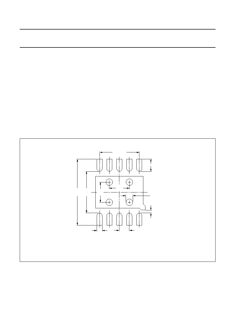
HVSON10: plastic, heatsink very thin small outline package; no leads;
10 terminals; body 3 x 3 x 0.90 mm
A
max.
A
A4
detail X
y
y1 C
Dh
Eh
Bottom view
e
L
b
10
5
1
6
X
D
E
C
B
A
w M
M
v
B
01-01-22
terminal 1
index area

2001 Nov 21
23
Philips Semiconductors
Product specification
Dual-band power amplifier controller for
GSM, PCN and DCS
PCF5079
14 SOLDERING (TSSOP10)
14.1
Introduction to soldering surface mount
packages
This text gives a very brief insight to a complex technology.
A more in-depth account of soldering ICs can be found in
our
"Data Handbook IC26; Integrated Circuit Packages"
(document order number 9398 652 90011).
There is no soldering method that is ideal for all surface
mount IC packages. Wave soldering is not always suitable
for surface mount ICs, or for printed-circuit boards with
high population densities. In these situations reflow
soldering is often used.
14.2
Reflow soldering
Reflow soldering requires solder paste (a suspension of
fine solder particles, flux and binding agent) to be applied
to the printed-circuit board by screen printing, stencilling or
pressure-syringe dispensing before package placement.
Several methods exist for reflowing; for example,
infrared/convection heating in a conveyor type oven.
Throughput times (preheating, soldering and cooling) vary
between 100 and 200 seconds depending on heating
method.
Typical reflow peak temperatures range from
215 to 250
°
C. The top-surface temperature of the
packages should preferable be kept below 230
°
C.
14.3
Wave soldering
Conventional single wave soldering is not recommended
for surface mount devices (SMDs) or printed-circuit boards
with a high component density, as solder bridging and
non-wetting can present major problems.
To overcome these problems the double-wave soldering
method was specifically developed.
If wave soldering is used the following conditions must be
observed for optimal results:
·
Use a double-wave soldering method comprising a
turbulent wave with high upward pressure followed by a
smooth laminar wave.
·
For packages with leads on two sides and a pitch (e):
larger than or equal to 1.27 mm, the footprint
longitudinal axis is preferred to be parallel to the
transport direction of the printed-circuit board;
smaller than 1.27 mm, the footprint longitudinal axis
must be parallel to the transport direction of the
printed-circuit board.
The footprint must incorporate solder thieves at the
downstream end.
·
For packages with leads on four sides, the footprint must
be placed at a 45
°
angle to the transport direction of the
printed-circuit board. The footprint must incorporate
solder thieves downstream and at the side corners.
During placement and before soldering, the package must
be fixed with a droplet of adhesive. The adhesive can be
applied by screen printing, pin transfer or syringe
dispensing. The package can be soldered after the
adhesive is cured.
Typical dwell time is 4 seconds at 250
°
C.
A mildly-activated flux will eliminate the need for removal
of corrosive residues in most applications.
14.4
Manual soldering
Fix the component by first soldering two
diagonally-opposite end leads. Use a low voltage (24 V or
less) soldering iron applied to the flat part of the lead.
Contact time must be limited to 10 seconds at up to
300
°
C.
When using a dedicated tool, all other leads can be
soldered in one operation within 2 to 5 seconds between
270 and 320
°
C.

2001 Nov 21
24
Philips Semiconductors
Product specification
Dual-band power amplifier controller for
GSM, PCN and DCS
PCF5079
14.5
Suitability of surface mount IC packages for wave and reflow soldering methods
Notes
1. All surface mount (SMD) packages are moisture sensitive. Depending upon the moisture content, the maximum
temperature (with respect to time) and body size of the package, there is a risk that internal or external package
cracks may occur due to vaporization of the moisture in them (the so called popcorn effect). For details, refer to the
Drypack information in the
"Data Handbook IC26; Integrated Circuit Packages; Section: Packing Methods".
2. These packages are not suitable for wave soldering as a solder joint between the printed-circuit board and heatsink
(at bottom version) can not be achieved, and as solder may stick to the heatsink (on top version).
3. If wave soldering is considered, then the package must be placed at a 45
°
angle to the solder wave direction.
The package footprint must incorporate solder thieves downstream and at the side corners.
4. Wave soldering is only suitable for LQFP, TQFP and QFP packages with a pitch (e) equal to or larger than 0.8 mm;
it is definitely not suitable for packages with a pitch (e) equal to or smaller than 0.65 mm.
5. Wave soldering is only suitable for SSOP and TSSOP packages with a pitch (e) equal to or larger than 0.65 mm; it is
definitely not suitable for packages with a pitch (e) equal to or smaller than 0.5 mm.
PACKAGE
SOLDERING METHOD
WAVE
REFLOW
(1)
BGA, LFBGA, SQFP, TFBGA
not suitable
suitable
HBCC, HLQFP, HSQFP, HSOP, HTQFP, HTSSOP, SMS
not suitable
(2)
suitable
PLCC
(3)
, SO, SOJ
suitable
suitable
LQFP, QFP, TQFP
not recommended
(3)(4)
suitable
SSOP, TSSOP, VSO
not recommended
(5)
suitable
2001 Nov 21
25
Philips Semiconductors
Product specification
Dual-band power amplifier controller for
GSM, PCN and DCS
PCF5079
15 SOLDERING (HVSON10)
15.1
Soldering information
Information contained within this chapter is of a preliminary
nature and may change without notice.
15.2
PCB design guidelines
These guidelines are to help the user in developing the
proper PCB design. For the surface mount process refer to
"Data Handbook IC26; Integrated Circuit Packages"
(document order number 9398 652 90011).
15.2.1
P
ERIMETER PAD DESIGN
Referring to Fig.20, dimensions Z and G are respectively
the outside to outside and the inside to inside pad
dimensions.
The dimensions X and Y indicate respectively the width
and the length of the pad. Note that the calculated
X dimension is the maximum value in order to avoid solder
bridging between adjacent pads.The calculated
Y dimension is the minimum value and therefore pad
design should start with this value and the pad length at
the outside be extended if more solder joint fillets are
required.
The dimension `Cpl' defines the minimum distance
between the inner tip of the pad and the outer edge of the
thermal pad. It is suggested that this dimension be fixed at
0.15 mm to avoid solder bridging issues between the
thermal pad and the perimeter pads.
handbook, full pagewidth
MGW498
Cpl = 0.15
0.33
0.30
thermal via
Z =
3.46
3.27
Y =
0.69
0.55
G =
2.09
1.20
1.00
X = 0.28
0.50
TYP
2.00 REF
1.20
1.00
Fig.20 HVSON10 PCB pattern.
Dimensions in mm.
The solder mask opening dimension should be larger than the pad dimension by 125 to 150
µ
m.
15.2.2
T
HERMAL PAD AND VIA DESIGN
The size of the thermal pad should at least match the size
of the exposed die-attach paddle. However, in some
cases, the die-attach paddle size may need to be modified
to avoid solder bridging between the thermal pad and the
perimeter pads. In order to effectively transfer heat from
the top metal layer to the inner or bottom layers of the
PCB, thermal vias should be incorporated into the thermal
pad design. The number of thermal vias will depend on the
application and on the power dissipation and electrical
requirements. It is recommended to incorporate an array
of thermal vias at a pitch of 1.0 to 1.2 mm with the via
diameter between 0.3 and 0.33 mm.

2001 Nov 21
26
Philips Semiconductors
Product specification
Dual-band power amplifier controller for
GSM, PCN and DCS
PCF5079
15.2.3
S
TENCIL DESIGN FOR PERIMETER PADS
For optimum paste release the area and aspect ratios of
the stencil should be greater than 0.66 and 1.5
respectively.
where:
L = aperture length
W = aperture width
T = stencil thickness.
15.2.4
S
TENCIL DESIGN FOR THERMAL PADS
In order to remove the heat effectively from the package
and to enhance electrical performance the die-attach
paddle needs to be soldered to the PCB thermal pad,
preferably with minimum voids.
It is therefore recommended that smaller, multiple
openings in a stencil should be used instead of one large
opening for printing solder paste in the thermal pad region.
This results typically in 50% to 80% solder paste coverage.
Two examples are shown in Fig.21.
15.2.5
S
TENCIL THICKNESS
A stencil thickness of 0.125 to 0.150 mm is recommended
but this value needs to be optimized by the user to find the
proper thickness according to application requirements.
Area ratio
area of aperture opening
aperture wall area
-----------------------------------------------------------------
L
W
×
2T(L + W)
--------------------------
=
=
Aspect ratio
aperture width
stencil thickness
-------------------------------------------
W
T
-----
=
=
handbook, full pagewidth
MGW499
Fig.21 Examples of thermal pad stencil design.
a. Outline of 0.4 mm
2
2
×
2 array giving
44% solder paste coverage.
b. Outline of 1.2 mm
2
2
×
1 array giving
60% solder paste coverage.

2001 Nov 21
27
Philips Semiconductors
Product specification
Dual-band power amplifier controller for
GSM, PCN and DCS
PCF5079
16 DATA SHEET STATUS
Notes
1. Please consult the most recently issued data sheet before initiating or completing a design.
2. The product status of the device(s) described in this data sheet may have changed since this data sheet was
published. The latest information is available on the Internet at URL http://www.semiconductors.philips.com.
DATA SHEET STATUS
(1)
PRODUCT
STATUS
(2)
DEFINITIONS
Objective data
Development
This data sheet contains data from the objective specification for product
development. Philips Semiconductors reserves the right to change the
specification in any manner without notice.
Preliminary data
Qualification
This data sheet contains data from the preliminary specification.
Supplementary data will be published at a later date. Philips
Semiconductors reserves the right to change the specification without
notice, in order to improve the design and supply the best possible
product.
Product data
Production
This data sheet contains data from the product specification. Philips
Semiconductors reserves the right to make changes at any time in order
to improve the design, manufacturing and supply. Changes will be
communicated according to the Customer Product/Process Change
Notification (CPCN) procedure SNW-SQ-650A.
17 DEFINITIONS
Short-form specification
The data in a short-form
specification is extracted from a full data sheet with the
same type number and title. For detailed information see
the relevant data sheet or data handbook.
Limiting values definition
Limiting values given are in
accordance with the Absolute Maximum Rating System
(IEC 60134). Stress above one or more of the limiting
values may cause permanent damage to the device.
These are stress ratings only and operation of the device
at these or at any other conditions above those given in the
Characteristics sections of the specification is not implied.
Exposure to limiting values for extended periods may
affect device reliability.
Application information
Applications that are
described herein for any of these products are for
illustrative purposes only. Philips Semiconductors make
no representation or warranty that such applications will be
suitable for the specified use without further testing or
modification.
18 DISCLAIMERS
Life support applications
These products are not
designed for use in life support appliances, devices, or
systems where malfunction of these products can
reasonably be expected to result in personal injury. Philips
Semiconductors customers using or selling these products
for use in such applications do so at their own risk and
agree to fully indemnify Philips Semiconductors for any
damages resulting from such application.
Right to make changes
Philips Semiconductors
reserves the right to make changes, without notice, in the
products, including circuits, standard cells, and/or
software, described or contained herein in order to
improve design and/or performance. Philips
Semiconductors assumes no responsibility or liability for
the use of any of these products, conveys no licence or title
under any patent, copyright, or mask work right to these
products, and makes no representations or warranties that
these products are free from patent, copyright, or mask
work right infringement, unless otherwise specified.

© Koninklijke Philips Electronics N.V. 2001
SCA73
All rights are reserved. Reproduction in whole or in part is prohibited without the prior written consent of the copyright owner.
The information presented in this document does not form part of any quotation or contract, is believed to be accurate and reliable and may be changed
without notice. No liability will be accepted by the publisher for any consequence of its use. Publication thereof does not convey nor imply any license
under patent- or other industrial or intellectual property rights.
Philips Semiconductors a worldwide company
Contact information
For additional information please visit http://www.semiconductors.philips.com.
Fax: +31 40 27 24825
For sales offices addresses send e-mail to: sales.addresses@www.semiconductors.philips.com.
Printed in The Netherlands
403506/01/pp
28
Date of release:
2001 Nov 21
Document order number:
9397 750 07095