
DATA SHEET
Product specification
Supersedes data of 1995 Apr 27
File under Integrated Circuits, IC17
1997 Mar 04
INTEGRATED CIRCUITS
PCF5001
POCSAG Paging Decoder

1997 Mar 04
2
Philips Semiconductors
Product specification
POCSAG Paging Decoder
PCF5001
CONTENTS
1
FEATURES
2
APPLICATIONS
3
GENERAL DESCRIPTION
4
ORDERING INFORMATION
5
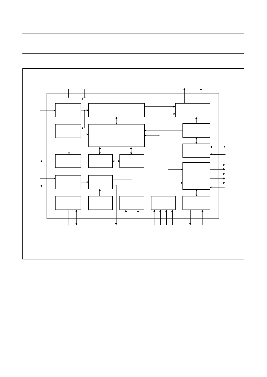
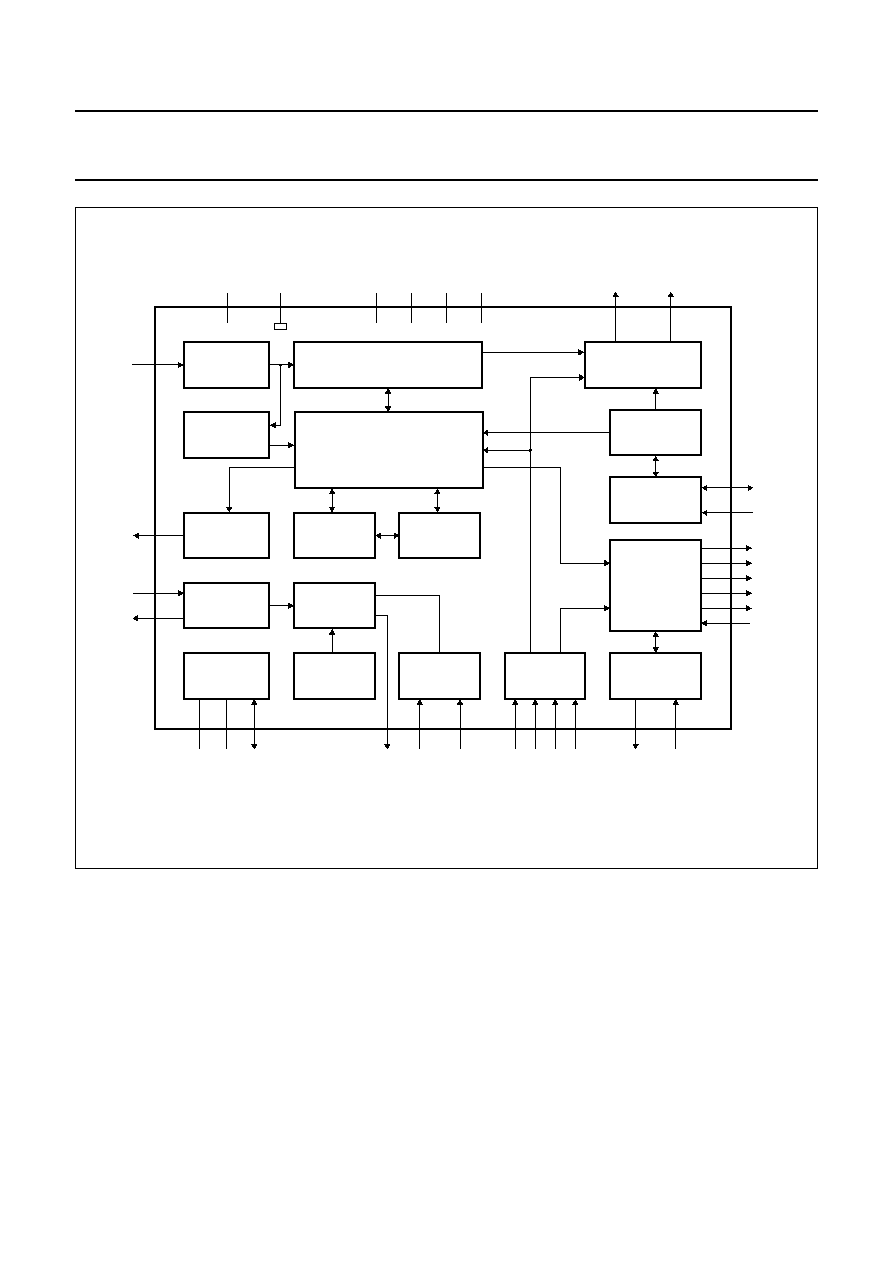
BLOCK DIAGRAMS
6
PINNING
7
FUNCTIONAL DESCRIPTION
7.1
The PCF5001 supports two basic modes of
operation
7.2
The POCSAG paging code
7.3
Modes and states of the decoder
7.4
Decoding of the POCSAG data stream
7.5
Generation of output signals
7.6
Alerter
7.7
Silent call storage and Repeat mode
7.8
Duplicate Call Suppression
7.9
LED indicator
7.10
Vibrator output
7.11
Start-up alert
7.12
Serial communication interface
7.13
Message data transfer
7.14
Call Data output on LED
7.15
Serial communication call data format
7.16
Data conversion
7.17
Memory Organization
7.18
Description of the Special Programmed
Function (SPF) bits
7.19
EEPROM Write operation
7.20
EEPROM Read operation
7.21
Read-back operation via Microcontroller
Interface
7.22
Voltage converter
7.23
Test modes of the decoder
7.23.1
Board test mode
7.23.2
Pager Test Mode (Type Approval Mode)
8
LIMITING VALUES
9
DC CHARACTERISTICS
10
DC CHARACTERISTICS (WITH VOLTAGE
CONVERTER)
11
AC CHARACTERISTICS
12
TIMING CHARACTERISTICS
13
PROGRAMMING CHARACTERISTICS
14
APPLICATION INFORMATION
15
PACKAGE OUTLINES
16
SOLDERING
16.1
Introduction
16.2
Reflow soldering
16.3
Wave soldering
16.3.1
LQFP
16.3.2
SO
16.3.3
Method (LQFP and SO)
16.4
Repairing soldered joints
17
DEFINITIONS
18
LIFE SUPPORT APPLICATIONS

1997 Mar 04
3
Philips Semiconductors
Product specification
POCSAG Paging Decoder
PCF5001
1
FEATURES
·
Wide operating supply voltage range (1.5 to 6.0 V)
·
Extended temperature range:
-
40 to +85
°
C (between
-
40 to
-
10
°
C, minimum supply voltage restricted
to 1.8 V)
·
Very low supply current (60
µ
A typ. with
76.8 kHz crystal)
·
"CCIR radio paging Code No 1" (POCSAG) compatible
·
Programmable call termination conditions
·
512 and 1200 bits/s data rates (2400 bits/s with some
restrictions), see Section 7.4
·
Improved ACCESS
®
synchronization algorithm
·
Supports 4 user addresses (RICs) in two independent
frames
·
Eight different alert cadences
·
Directly drives magnetic or piezo ceramic beeper
·
High level alert requires only a single external transistor
·
Optional vibrator type alerting
·
Silent call storage, up to eight different calls
·
Repeat alarm facility
·
Programmable duplicate call suppression
·
Interfaces directly to UAA2050T, UAA2080 and
UAA2082 digital paging receivers
·
Programmable receiver power control for battery
economy
·
On-chip non-volatile EEPROM storage
·
On-chip voltage converter with improved drive capability
·
Serial microcontroller interface for display pager
applications
·
Optional visual indication of received call data using a
modified RS232 format
·
Level shifted microcontroller interface signals
·
Alert on low battery
·
Optional out-of-range indication.
2
APPLICATIONS
·
Alert-only pagers, display pagers
·
Telepoint
·
Telemetry/data receivers.
3
GENERAL DESCRIPTION
The PCF5001 is a fully integrated low-power decoder and
pager controller. It decodes the CCIR radio paging Code
No.1 (POCSAG-Code) at 512 and 1200 bits/s data rates.
The PCF5001 is fabricated in SACMOS technology to
ensure low power consumption at low supply voltages.
4
ORDERING INFORMATION
Note
1. When using IR reflow soldering it is recommended that the Drypack instructions in the
"Quality Reference Handbook"
(order number 9397 750 00192) are followed.
TYPE NUMBER
PACKAGE
NAME
DESCRIPTION
VERSION
PCF5001T
SO28
plastic small outline package; 28 leads; body width 7.5 mm
SOT136-1
PCF5001H
LQFP32
(1)
plastic low profile quad flat package; 32 leads; body 7
×
7
×
1.4 mm
SOT358-1
1997 Mar 04
4
Philips Semiconductors
Product specification
POCSAG Paging Decoder
PCF5001
5
BLOCK DIAGRAMS
Fig.1 Block diagram (SO28; SOT136-1).
handbook, full pagewidth
PD
PS
DO
DS
PCF5001T
RECEIVER
ENABLE
CONTROL
OSCILLATOR
VOLTAGE
CONVERTER
POWER-ON
RESET
TEST
CONTROL
STATUS
CONTROL
CLOCK
RECOVERY
CLOCK
GENERATION
DATA OUTPUT
CONTROL
DIGITAL INPUT
FILTER
SYNC
CONTROL
TIMING
CONTROL
DECODER AND
ERROR CORRECTION
CONTROL
BL
BS
SR SK ON IE
EEPROM
MEMORY
EEPROM
CONTROL
ALERT
GENERATION
CONTROL
BATTERY LOW
CONTROL
SERIAL DATA PROCESSOR
26
27
AH
AL
OR
OM
OL
AI
DI
TS
TT
FL
CP
CN
RE
X1
X2
12
15
25
16
13
23
Vref
VSS
VDD
5
14
9
10
7
8
17
4
3
2
1
28
11
18
21 20 22 19
24
6
MCD454
1997 Mar 04
5
Philips Semiconductors
Product specification
POCSAG Paging Decoder
PCF5001
Fig.2 Block diagram (LQFP32; SOT358-1).
handbook, full pagewidth
PD
PS
DO
DS
PCF5001H
RECEIVER
ENABLE
CONTROL
OSCILLATOR
VOLTAGE
CONVERTER
POWER-ON
RESET
TEST
CONTROL
STATUS
CONTROL
CLOCK
RECOVERY
CLOCK
GENERATION
DATA OUTPUT
CONTROL
DIGITAL INPUT
FILTER
SYNC
CONTROL
TIMING
CONTROL
DECODER AND
ERROR CORRECTION
CONTROL
BL
BS
SR SK ON IE
EEPROM
MEMORY
EEPROM
CONTROL
ALERT
GENERATION
CONTROL
BATTERY LOW
CONTROL
SERIAL DATA PROCESSOR
10
11
AH
AL
OR
OM
OL
AI
DI
TS
TT
FL
CP
CN
RE
X1
X2
26
29
9
30
27
6
Vref
VDD
17
28
23
24
19
22
VSS
31
16
15
14
13
12
25
32
4
3
5
1
8
18
MLB045
n.c.
2
n.c.
7
n.c.
20
n.c.
21

1997 Mar 04
6
Philips Semiconductors
Product specification
POCSAG Paging Decoder
PCF5001
6
PINNING
SYMBOL
PIN
DESCRIPTION
PCF5001T
(SOT136-1)
PCF5001H
(SOT358-1)
V
ref
1
13
Microcontroller interface reference voltage input/output. The LOW level of
pins FL, DS, DO, OR, BL, AI, ON, SK, SR and IE is related to the voltage
on V
ref
. May be driven from an external negative voltage source or must
be connected to V
SS
, if pins CN and CP are left open-circuit. When the
on-chip voltage converter is used, this pin provides a doubled negative
output voltage.
CN
2
14
Voltage converter external shunt capacitance, negative side. Connect the
negative side of the shunt capacitor to this pin, if the on-chip voltage
converter function is used.
CP
3
15
Voltage converter external shunt capacitor, positive side. Connect the
positive side of the shunt capacitor to this pin, if the on-chip voltage
converter function is used.
V
DD
4
16
Main positive power supply. This pin is common to all supply voltages and
is referred to as 0 V (common).
DI
5
17
Serial data input (POCSAG code). The serial data signal train applied to
this pin is processed by the decoder. Pulled LOW by an on-chip pull-down
when the receiver is disabled (RE = LOW).
BS
6
18
Battery-low indication input. The decoder samples this input during
synchronization scan, when it is in ON or SILENT status and the receiver
is enabled (RE = HIGH). A battery-low condition is assumed, if the
decoder detects four consecutive samples HIGH. An audible battery-low
indication is made by the decoder, when operating in ON status. Normally
LOW by the operation of an on-chip pull-down.
PD
7
19
EEPROM programming data input and output. Normally HIGH by the
operation of an on-chip pull-up. During programming of the on-chip
EEPROM, PD is a bidirectional data and control signal.
PS
8
22
EEPROM programming strobe input. Normally LOW by the operation of
an on-chip pull-down. During programming of the on-chip EEPROM, PS is
a unidirectional control input.
X1
9
23
Crystal oscillator input. Connect a 32768 Hz or 76800 Hz crystal and a
biasing resistor between this pin and X2. In addition, provide a load
capacitance to V
DD
, which may also be used for frequency tuning.
X2
10
24
Crystal oscillator output. Return connection for the external crystal and
resistor at X1.
TS
11
25
Scan test mode enable input. Always LOW by operation of an on-chip
pull-down.
AH
12
26
Alert HIGH-level output. This output can directly drive an external bipolar
transistor to control HIGH-level alerting in conjunction with AL, by means
of an alerter or beeper.
OL
13
27
LED indication output. This output can directly drive an external bipolar
transistor to control the visual alert function by means of an LED. It may
also be used for visual indication of received call data during call
reception.

1997 Mar 04
7
Philips Semiconductors
Product specification
POCSAG Paging Decoder
PCF5001
RE
14
28
Receiver enable output. May be used to control the paging receiver power
control input, to minimize power consumption. The decoder provides a
HIGH-level at this pin, when receiver operation is requested. Each time
the decoder does not require any input data at DI the receiver enable
output is LOW.
AL
15
29
Alert LOW-level output. Open drain alert output in anti-phase to AH, to
provide LOW-level alerting. HIGH-level alerting is generated in conjunction
with AH.
OM
16
30
Vibrator output. This output can directly drive an external bipolar transistor
to control a vibrator type alerter.
V
SS
17
31
Main negative supply voltage.
TT
18
32
Test mode enable input. Always LOW by operation of an on-chip
pull-down.
IE
19
1
Interface enable input. While the interface enable input is active HIGH,
operation of the ON, SK, SR, AI, BL and OR inputs and outputs is
possible. When IE is LOW the inputs do not respond to applied signals
and the outputs are made high-impedance. In alert-only pager mode the
interface enable input does not have any effect on the operation of inputs
ON, SK and SR, but IE must be referenced to LOW or HIGH.
SK
20
3
SILENT state control input. The SILENT control input selects the decoder
ON status (LOW-level) or SILENT status (HIGH-level), if the ON input is
active HIGH. An on-chip pull-up is provided, if the decoder has been
programmed for `alert-only pager' mode, whereby the pull-up is disabled
for display pager mode. In `display pager' mode status change is
possible if the interface enable input (IE) is HIGH and the status is latched
on the falling edge of IE.
SR
21
4
Status request and reset input. A HIGH-going pulse on this input causes
(a) status indication cadence to be generated, if the decoder is not alerting
or (b) resetting of a call alert, repeated call alert or battery-low alert, if
active or (c) triggers the call store re-alert facility, if repeat mode is active.
In `display pager' mode operation of SR is possible only if the interface
control input is active. Normally LOW by the operation of an on-chip
pull-down.
ON
22
5
On/off control input. The on/off control input selects the decoder ON status
(HIGH-level) or OFF status (LOW-level). An on-chip pull-up resistor is
provided, if the decoder has been programmed for `alert-only pager' mode,
but the pull-up resistor is disabled for `display pager' mode. In
`display pager' mode, status change is possible if the interface enable
input (IE) is HIGH and the status is latched on the falling edge of IE.
AI
23
6
Alarm input. A HIGH-level on this input causes generation of a continuous
HIGH-level alert via AH and AL outputs, if the decoder operates in ON
status or OFF status. In addition, the LED output is active independent
from the decoder status, but in accordance with AI. Pulsing the input may
be used to modulate the alert and LED indication. Normally LOW in
`alert-only pager' mode by operation of an on-chip pull-down.
SYMBOL
PIN
DESCRIPTION
PCF5001T
(SOT136-1)
PCF5001H
(SOT358-1)

1997 Mar 04
8
Philips Semiconductors
Product specification
POCSAG Paging Decoder
PCF5001
BL
24
8
Battery-low indication output. If the decoder encounters a battery-low
condition a battery-low output latch is set HIGH. The battery-low output
latch may be tested for a battery-low condition, whenever the interface
enable input (IE) is active (HIGH), otherwise the battery-low output is
made high-impedance. The battery-low output latch is reset only, by
switching the decoder to OFF status.
OR
25
9
Out-of-range indication output. Whenever the decoder detects an
out-of-range condition an out-of-range output latch is set HIGH after expiry
of the programmed out-of-range hold-off time selected by means of
special programming (SPF06 and SPF07) of the EEPROM. The
out-of-range latch may be tested for an out-of-range condition, whenever
the interface enable input (IE) is active (HIGH), otherwise the out-of-range
output is made high-impedance. The out-of- range output is reset by
detection of a valid data transmission or by switching the decoder to OFF
status.
DO
26
10
Serial interface data output. During normal decoder operation, accepted
calls and possibly subsequent message data are serially output via this pin
in conjunction with the data strobe output (DS). This pin is also used to
output the EEPROM contents upon special command, if the decoder is
programmed for display pager.
DS
27
11
Serial interface data strobe output. Provides a clock signal for the received
call data and EEPROM data appearing at the data output (DO). Each time
this output is LOW the data at DO is valid. Additional start and stop
conditions allow easy identification of data sequence start and end.
FL
28
12
Frequency reference output. When programmed for `display pager' mode,
this output provides a clock reference with 16384 or 32768 Hz per
second, selected by SPF32. See Chapter 7.
n.c.
-
2, 7, 20, 21
Not connected.
SYMBOL
PIN
DESCRIPTION
PCF5001T
(SOT136-1)
PCF5001H
(SOT358-1)

1997 Mar 04
9
Philips Semiconductors
Product specification
POCSAG Paging Decoder
PCF5001
Fig.3 Pin configuration PCF5001T (SOT136-1).
handbook, halfpage
28
27
26
25
24
23
22
21
20
19
18
17
16
15
1
2
3
4
5
6
7
8
9
10
11
12
13
14
MCD455 - 1
DS
DO
OR
BL
AI
ON
SR
SK
IE
TT
OM
AL
FL
PCF5001T
CN
CP
DI
BS
PD
PS
X1
X2
TS
AH
OL
RE
Vref
VDD
VSS
Fig.4 Pin configuration PCF5001H (SOT358-1).
handbook, halfpage
1
2
3
4
5
6
7
8
24
23
22
21
20
19
18
17
9
10
11
12
13
14
15
16
32
31
30
29
28
27
26
25
index
corner
IE
n.c.
SK
SR
ON
AI
n.c.
BL
OR
DO
DS
FL
V
ref
CN
CP
V
DD
DI
BS
PD
n.c.
n.c.
PS
X1
X2
TS
AH
OL
RE
AL
OM
V
SS
TT
PCF5001H
MLB048
7
FUNCTIONAL DESCRIPTION
The PCF5001 is a very low power Decoder and Pager
Controller specifically designed for use in new generation
radio pagers. The architecture of the PCF5001 allows for
flexible application in a wide variety of radio pager designs.
The PCF5001 is fully compatible with
"CCIR radio paging
Code Number 1" (also known as the POCSAG code)
operating at the originally specified 512 bits/s data rate,
and also at the newly specified 1200 bits/s data rate
(2400 bits/s operation is also possible). The PCF5001 also
offers features which extend the basic flexibility and
efficiency of this code standard.
7.1
The PCF5001 supports two basic modes of
operation
In alert-only pager mode only a minimum number of
external components are required to build a complete
tone-only pager. Selection of operating states ON, OFF or
SILENT is achieved using a slider switch interface.
In display pager mode the state input logic is switched to
a bus interface structure. Received calls and messages
are transferred to an external microcontroller via the serial
microcontroller interface. A built-in voltage converter with
increased drive capabilities can supply doubled supply
voltage output, and appropriate logic level shifting on
microcontroller interface signals is provided.
Upon reception of valid calls one of eight different call
cadences is generated; upon status interrogation status
indication tones make the current status of the decoder
available to the user.
On-chip non-volatile 114-bit EEPROM storage is provided
to hold up to four user addresses, two frame numbers and
the programmed decoder configuration.
Synchronization to the input data stream is achieved using
the improved ACCESS
®
algorithm, which allows for data
synchronization and re-synchronization without preamble
detection while minimizing battery power consumption by
receiver power control. One of four error correction
algorithms is applied to the received data to optimize the
call success rate.

1997 Mar 04
10
Philips Semiconductors
Product specification
POCSAG Paging Decoder
PCF5001
7.2
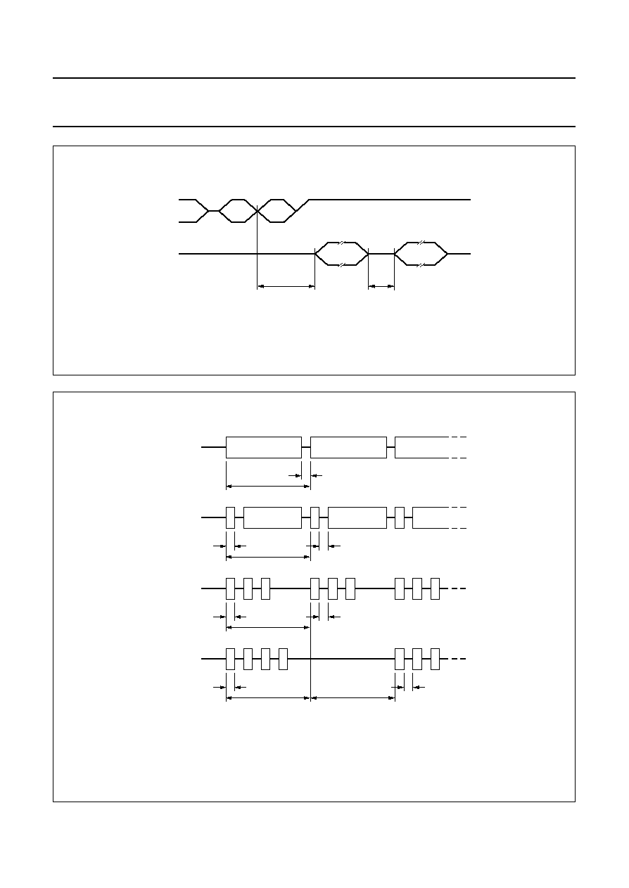
The POCSAG paging code
A transmission using the
"CCIR Radio paging Code No. 1"
(POCSAG code) is constructed in accordance with the
following rules (see Fig.5).
The transmission is started by sending a preamble,
consisting of at least 576 continuously alternating bits
(10101010...). The preamble is followed by an arbitrary
number of batch blocks. Only complete batches are
transmitted.
Each batch comprises 17 codewords of 32 bits each.
The first codeword is a synchronization codeword with a
fixed pattern. The sync word is followed by 8 frames
(0 to 7) of 2 codewords each, containing message
information. A codeword in a frame can either be an
address, message or idle codeword.
Idle codewords also have a fixed pattern and are used to
fill empty frames or to separate messages.
Address codewords are identified by an MSB at logic 0
and are coded as shown in Fig.5. A user address or RIC
consists of 21 bits. Only the upper 18 bits are encoded in
the address codeword (bits 2 to 19). The lower 3 bits
designate the frame number (0 to 7) in which the address
is transmitted.
Four different call types (`numeric', `alphanumeric' and two
`alert only' types) can be distinguished. The call type is
determined by two function bits in the address codeword
(bits 20 and 21).
Alert-only calls consist only of a single address codeword.
Numeric and alphanumeric calls have message
codewords following the address. A message causes the
frame structure to be temporarily suspended. Message
codewords are sent until the message is completed, with
only the sync words being transmitted in their expected
positions.
Message codewords are identified by an MSB at logic 1
and are coded as shown in Fig.5. The message
information is stored in a 20-bit field (bits 2 to 21).
The standard data format is determined by the call type: 4
bits per digit for numeric messages and 7 bits per (ASCII)
character for alphanumeric messages.
Each codeword is protected against transmission errors by
10 CRC check bits (bits 22 to 31) and an even-parity bit
(bit 32). This permits correction of a maximum of 2 random
errors or up to 3 errors in a burst of 4 bits (a 4-bit burst
error) per codeword.
Fig.5 POCSAG code structure.
handbook, full pagewidth
PREAMBLE
BATCH 1
BATCH 2
BATCH 3
LAST BATCH
SYNC | CW CW | CW CW | . . . . . | CW CW
FRAME 0
FRAME 1
FRAME 7
10101 . . . 10101010
Address code-word
Message code-word
0
18-bit address
2 function bits
10 CRC bits
P
1
20-bit message
10 CRC bits
P
MCD456

1997 Mar 04
11
Philips Semiconductors
Product specification
POCSAG Paging Decoder
PCF5001
7.3
Modes and states of the decoder
The PCF5001 supports two basic operating modes:
·
`Alert-only pager' mode
·
`Display pager' mode.
Two further modes, the programming mode and the test
mode, are implemented to program and verify the
EEPROM contents and to support pager production and
approval tests, respectively.
In `alert-only pager' mode no external microcontroller is
required, see Fig.22. A three position slider switch
interface is provided to select the internal state of the
decoder. The decoder performs regular scanning of the
switch inputs to detect a status change. A push-button
interface is provided on the SR input, which is used as
input for user acknowledgment actions and status
interrogation. Upon reception of valid calls, tone alert
cadences are generated. A call storage is provided to store
calls received while operating in SILENT status and to
recall cadences upon `repeat' mode operation.
The voltage doubler and the frequency reference output
are disabled in this mode.
In `display pager' mode the PCF5001 operates as decoder
and pager controller in combination with an external
microcontroller (see Fig.23). The internal states of the
decoder are determined by appropriate logic levels on the
status inputs. A bus type interface structure is used to
interface the decoder to the microcontroller. The decoder's
on-chip voltage converter provides doubled supply voltage
output to provide a higher supply voltage to the
microcontroller and any additional hardware. The logic
levels of the interface's input and output signals are level
shifted to allow for direct coupling between microcontroller
and the decoder. Upon detection of a valid call, address
and message information are transferred to the external
microcontroller using the serial microcontroller interface.
In addition, appropriate call alert cadences are generated.
If the decoder is in one of the two operating modes, it is
always in one of the following three internal states:
·
OFF status. This is the power saving, inactive status of
the PCF5001. The paging receiver is disabled, no
decoding of input data takes place. However, the crystal
oscillator is kept running to ensure that scanning of the
status inputs/status switch is maintained to allow
changing into one of the following two active states.
·
ON status. This is the normal active status of the
decoder. Incoming calls are compared with the user
addresses stored in the internal EEPROM. Upon
detection of valid calls, alert cadences and LED
indication are generated and data is shifted out at the
serial microcontroller interface.
·
SILENT status. The SILENT status is the same as the
ON status with the exception that valid calls no longer
cause generation of call alert cadences. Instead, if
programmed as `alert-only pager', the decoder stores up
to eight different calls and generates appropriate alert
cadences after the decoder has been put back into the
ON status. However, special SILENT override calls will
cause generation of alert cadences, if enabled.
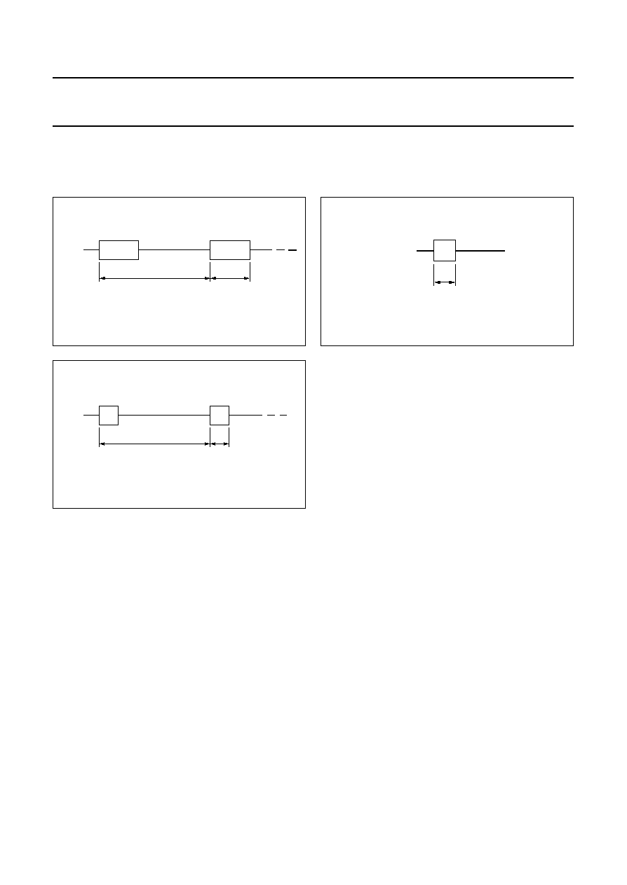
The decoder operating status is selected as indicated in
Table 1.
When programmed for `alert-only pager' a switch
debounce period is applied to the status inputs. For status
change and status interrogation in `display pager' mode,
see Figs 6 and 7.
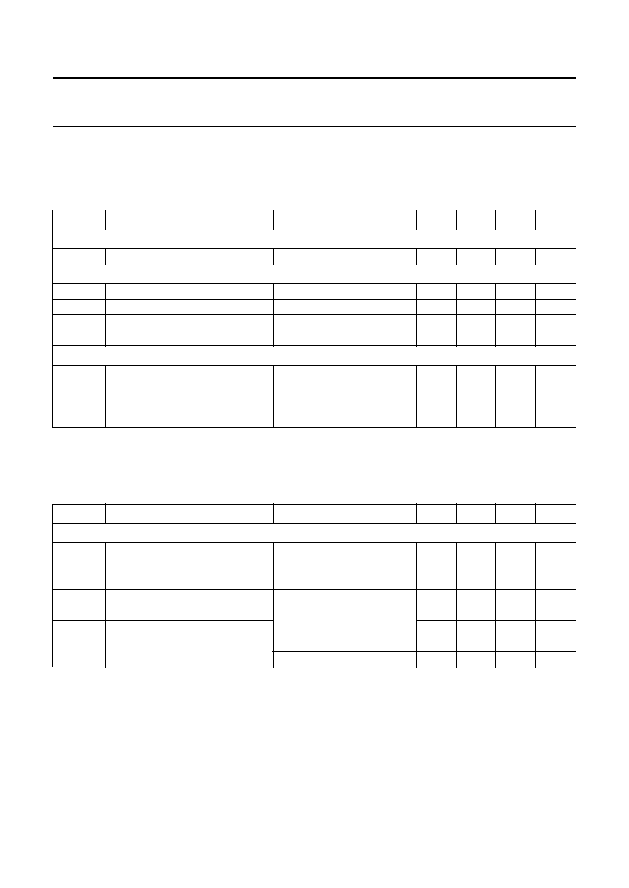
Table 1
Truth table for decoder operating status
Note
1. The EEPROM transfer mode applies to `display pager' mode only.
ON INPUT
SK INPUT
OPERATING STATUS
0
0
OFF
0
1
OFF (EEPROM transfer mode; note 1)
1
0
ON
1
1
SILENT

1997 Mar 04
12
Philips Semiconductors
Product specification
POCSAG Paging Decoder
PCF5001
Fig.6 Status change in display pager mode.
INTERNAL
STATUS
IE
ON
SK
t
t
t
STP
STD
STD
t IEH
t STH
MCD457 - 1
Fig.7 Status interrogation in display pager mode.
MCD458
IE
SR
t
t
t
t
t
STP
STH
SPD
IEH
STH
7.4
Decoding of the POCSAG data stream
The POCSAG coded input data stream is first noise filtered
by a digital filter. From the filtered data a sampling clock
synchronous to the data rate is derived. The PCF5001
supports 512 bits/s and 1200 bits/s data rates. This results
in a 512 Hz or 1200 Hz sampling clock frequency,
respectively. Synchronization on the POCSAG code
structure is performed using the improved Philips
ACCESS
®
algorithm, which employs a state machine with
six internal states.
A data rate of 2400 bits/s is possible if an external clock
generator of 153.6 kHz is connected to X1. The minimum
supply voltage is then
-
1.8 V.
The receiver enable output is activated a period equal to
t
RXON
before the input data is actually needed. The
decoder has first to achieve bit and word synchronization
before it can receive calls. The algorithm searches first for
the preamble and then for synchronization codeword
patterns.

1997 Mar 04
13
Philips Semiconductors
Product specification
POCSAG Paging Decoder
PCF5001
This is carried out for the duration of 3 batches in
power-on mode or 1 batch (=preamble duration) in
preamble receive mode. Error correction algorithms are
applied to the data before it is compared with preamble
and synchronization codeword patterns.
The synchronization process is terminated and thus
data receive mode is entered as soon as synchronization
codewords are seen at the beginning of each batch.
The decoder handles loss of synchronization in three
steps:
1. If the decoder fails to detect the synchronization
pattern at the beginning of the current batch it
continues data reception as normal. This data fail
mode is signalled in the message output when an
address codeword was received, as shown in Table 4.
2. If also at the beginning of the next batch no
synchronization codeword can be detected, the
algorithm assumes a small bit shift in the
fade recovery mode and performs more
synchronization codeword checks around the
expected position for the following 15 batches. Call
reception is suspended.
3. If it fails to re-synchronize in the `fade recovery' mode,
the carrier off mode is selected, in which the decoder
attempts to regain synchronization by bit-wise shifting
its synchronization scan window. Using this technique
re-synchronization is obtained within a continuous
data stream of at least 18 batches without preamble
detection.
In `data receive' mode, the input data stream is sampled at
the synchronization codeword position and the
programmed frame positions. The received codewords are
error corrected and then, if address codewords, compared
with the stored user addresses related to that frame.
On detection of a valid call, the decoder performs the
following three operations:
1. Set a store for call alert cadence generation according
to the combination of the function bits in the accepted
address codeword. The call alert cadence will not be
generated before the call has been terminated.
2. Keep the receiver enable output (RE) active and
receive subsequent message codewords, until any of
the call termination criteria are fulfilled.
3. Trigger the serial message transfer by sending a start
condition and transfer deformatted message
codewords as attached to the address codeword via
the serial microcontroller interface to an external
microcontroller, followed by a stop condition.
Normally call termination is assumed, when a valid idle or
address codeword is received. On reception of
uncorrectable codewords, call termination takes place in
accordance with conditions shown in Table 2.
Table 2
Call termination on error
Note
1. X = don't care.
SPF12
SPF13
CALL TERMINATION EVENT
0
X
(1)
Any two consecutive codewords or the codeword directly following the address
codeword uncorrectable.
1
0
Any single codeword uncorrectable.
1
1
Any two consecutive codewords uncorrectable.

1997 Mar 04
14
Philips Semiconductors
Product specification
POCSAG Paging Decoder
PCF5001
7.5
Generation of output signals
The PCF5001 provides output indications for call alert,
repeat mode alert, out of range alert, battery-low alert,
status indication alert and start-up alert. Some of the alert
functions may be freely configured by programming of
SPF bits within the EEPROM.
Table 3 shows the outputs which are used for special
output indications, if the decoder operates in ON status.
Remark: reception of special SILENT override calls
causes the decoder to generate call alert indication via AL
and AH even if it operates in SILENT status.
Table 3
Output signals
Note
1. Entries in parenthesis are not valid, if the decoder operates in SILENT status.
ALERT FUNCTION
OUTPUT ACTIVE
(1)
AL
AH
OL
OM
OR
BL
Start-up
(yes)
-
yes
yes
-
-
Status indication
yes
-
-
-
-
-
Call reception
(yes)
(yes)
yes
SPF11
-
-
Repeat mode
(SPF16)
(SPF16)
SPF16
-
-
-
Out-of-range
-
-
SPF15
-
yes
-
Battery-low
(yes)
(yes)
-
-
-
yes
Alarm input
(yes)
(yes)
yes
-
-
-
7.6
Alerter
The PCF5001 provides the AL and AH outputs for
acoustical LOW-level and HIGH-level signalling.
LOW-level alerting is provided by the AL output only.
For HIGH-level alerting both, AL and AH are active in
anti-phase. The square-wave output signals produce tone
alert cadences by means of a magnetic or piezo ceramic
beeper. The alert frequency, 2048 Hz or 2731 Hz
square-wave, is selected by programming of SPF31.
When valid calls are received while operating in ON status,
the PCF5001 generates call alert cadences. The first four
seconds are generated at LOW-level, a further twelve
seconds are generated at HIGH-level. Alert tone
generation and LED indication automatically terminate
after sixteen seconds unless terminated by pulsing the
status request and reset input (SR). Call alert generation
is inhibited until completion of message codeword
reception and the termination word is sent by the decoder.
Call alert generation commences after an alert delay
period, t
ALD
, at the earliest, see Fig.8. Call alert deletion is
possible during the alert delay period.
The call alert cadence is modulated according to the two
function bits (FC) in the received address codeword,
see Fig.9.
Valid calls received on RIC B or RIC D cause the alerter
frequency to be warbled by means of an additional 16 Hz
and 1024 Hz signal (respective 1365 Hz for SPF31 = 1)
as opposed to RIC A and RIC C where no alert frequency
warble takes place. Thus, eight different call cadences are
distinguishable.
ON status interrogation by the status request and reset
input (SR) the PCF5001 generates a status cadence at
LOW-level, in accordance with the present internal
decoder status (see Fig.10).
When detecting a battery-low condition the PCF5001
provides a battery-low indication. Operating in ON status
causes generation of a battery-low alert at HIGH-level for
sixteen seconds or until terminated by pulsing SR.
Operating in SILENT status or `repeat' mode the
battery-low alert is stored and inhibited until switching to
ON status.
1997 Mar 04
15
Philips Semiconductors
Product specification
POCSAG Paging Decoder
PCF5001
Fig.8 Call alert delay.
DO
DS
EOT
STP
CALL1
CALL2
AL
AH
OL
t
ALD
t
ALD
MCD459
Fig.9 Call alert cadences.
t ALP
tALC
t
ALC
tALP
MCD460
t
ALC
tALP
t ALP
t ALC
tALP
t ALP
t
ALC
tALP
cadence 1
(FC = 00)
cadence 2
(FC = 01)
cadence 3
(FC = 10)
cadence 4
(FC = 11)

1997 Mar 04
16
Philips Semiconductors
Product specification
POCSAG Paging Decoder
PCF5001
Fig.10 Status indication cadences.
MCD461
ON
OFF
SILENT
t STON
t STOF
t STON
t STOF
t STON
7.7
Silent call storage and repeat mode
When programmed for alert only pager the PCF5001
provides a call alert storage for storing of call alerts
received during SILENT status or for call alerts which
caused the decoder to enter repeat mode. Call alert is not
stored, when call indication is terminated by action of the
status request and reset input (SR).
Allowing the call indication to time-out by expiration of a
sixteen second alert operation causes the `repeat' mode to
be entered, while operating in ON status or SILENT status.
Such call alerts are stored for later repeated call alert on
interrogation by the user. When `repeat' mode has been
entered and the decoder operates in ON status, the repeat
call store is interrogated by pulsing the status request and
reset input (SR) or on switching to ON status if the decoder
operates in SILENT status. When SILENT override calls
are received, which entered the `repeat' mode,
interrogation of repeat call store operates as in decoder
ON status. After interrogation of repeat call store and
subsequent generation of all stored call alerts the call store
is cleared and the `repeat' mode is terminated.
When programmed by means of SPF16, a repeat alert
cadence is generated periodically, whenever `repeat'
mode has been entered. Operating in ON status causes
the repeat alert cadence to be generated at HIGH-level
and warbled by means of an additional 16 Hz and 1024 Hz
signal (respective 1365 Hz for SPF31 = 1) as shown in
Fig.11. The LED output indicates the same alert cadence
and alert warble. In SILENT status only the LED output is
active.
No call alert storage occurs when the decoder is
programmed for `display pager' mode.
7.8
Duplicate Call Suppression
The PCF5001 provides a Duplicate Call Suppression with
time-out facility, to identify duplicate call reception. When
selected by programming of SPF14, the PCF5001 inhibits
any duplicate call alert in `alert-only pager' mode.
In `display pager' mode, duplicate call indication is
achieved only via the serial microcontroller interface. A call
is assumed to be duplicate if its address and function bit
setting is equal to the latest received call, which initialized
the call address and function bit reference. The Duplicate
Call Suppression time-out is selectable by programming of
SPF06 and SPF07.
7.9
LED indicator
The PCF5001 provides for visual signalling using a LED
via output OL.
Call alert indication is provided by the LED with the same
cadence and warble modulation as for the alerter outputs
AL and AH. Call alert indication occurs in ON and SILENT
status and automatically terminates after sixteen seconds
time-out unless terminated by pulsing the status request
and reset input (SR).
When detecting an out-of-range condition and enabled by
programming of SPF15, the LED output provides an
out-of-range indication as shown in Fig.12.
1997 Mar 04
17
Philips Semiconductors
Product specification
POCSAG Paging Decoder
PCF5001
The LED output can be made to provide message data by
programming SPF17. Alert signals are inhibited during
message data transfer.
7.10
Vibrator output
The PCF5001 provides the OM output for activating a
vibrator-type alerter for call alert indication. The vibrator
output is enabled by programming of SPF11.
Calls received while operating in SILENT status cause
activation of the vibrator output for the normal call alert
cadence or until terminated by operation of the status
request and reset input (SR). SILENT override calls, calls
received in decoder ON status and repeated call alerts are
alerted normally by the AL and AH outputs.
7.11
Start-up alert
To indicate the establishment of operational condition
whenever the decoder status has been changed from OFF
to ON or SILENT status, the PCF5001 provides a start-up
alert indication. Switching from OFF to ON status causes
generation of a start-up alert cadence at LOW-level and on
the LED output OL (see Fig.13).
Fig.11 Repeat alert cadence.
MCD462
AL
AH
OL
t
RCR
t RPT
Fig.12 Out-of-range indication.
MCD463
t
t
ORA
ORD
When changing from OFF to SILENT status, the start-up
alert will be indicated on the LED output and the vibrator
output OM.
7.12
Serial communication interface
To transmit any call message data received to an external
microcontroller for post-processing, a serial
communication interface has been provided by a serial
data output signal DO and a data strobe signal DS as
shown in Fig.14.
Upon interrogation the PCF5001 is also able to transfer
EEPROM contents via the serial communication interface,
see Section 7.21.
7.13
Message data transfer
The transfer of message data via DO and DS is organized
in 8-bit words providing additional start and stop conditions
as shown in Fig.15.
On reception of a valid call address the PCF5001
generates a start condition and outputs an address word
as shown in Fig.15a.
The address word indicates call address, function bit
setting and decoder flags as shown in Table 4.
Message codewords received and concatenated to a valid
call address are transferred after completion of the
address word. The message bits received in the message
codewords are split into blocks and are converted to obtain
the message words. The message words comprise an
error flag to indicate message words, which are derived
from uncorrectable message codewords as shown in
Table 5.
Message data is output at a rate of 2048 bits/s with a
minimum delay of 2 bits between consecutive message
words.
Fig.13 Start-up alert.
MCD464
AL
OL
OM
t
SUA
1997 Mar 04
18
Philips Semiconductors
Product specification
POCSAG Paging Decoder
PCF5001
Termination of call reception causes a termination word to
be transferred, which indicates successful or unsuccessful
call termination as shown in Table 6.
Serial data transfer for a received call ends with a stop
condition as shown in Fig.15c.
MEA254 - 1
1st message word
address word
start condition
DO
DS
START OF TRANSFER
A0
A1
A2
A3
A4
A5
A6
A7
message word N+1
message word N
message word N1
MESSAGE TRANSFER
Mn0 Mn1 Mn2 Mn3 Mn4 Mn5 Mn6 Mn7
termination word
last message word
END OF TRANSFER
T0
T1
T2
T3
T4
T5
T6
T7
stop condition
DO
DS
DO
DS
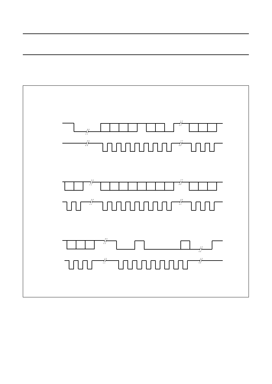
Fig.14 Call data transfer on the serial communication interface.

1997 Mar 04
19
Philips Semiconductors
Product specification
POCSAG Paging Decoder
PCF5001
handbook, full pagewidth
DO
DS
t
DSW
t DOH
t
DOS
t DSD
t TDO
DO
DS
t
ST
t
DOS
DO
DS
MEA253 - 2
t
DOH
t
SP
Fig.15 Serial communication interface timing.
a.
b.
a. Start condition.
b. Data bit.
c. Stop condition.
c.
1997 Mar 04
20
Philips Semiconductors
Product specification
POCSAG Paging Decoder
PCF5001
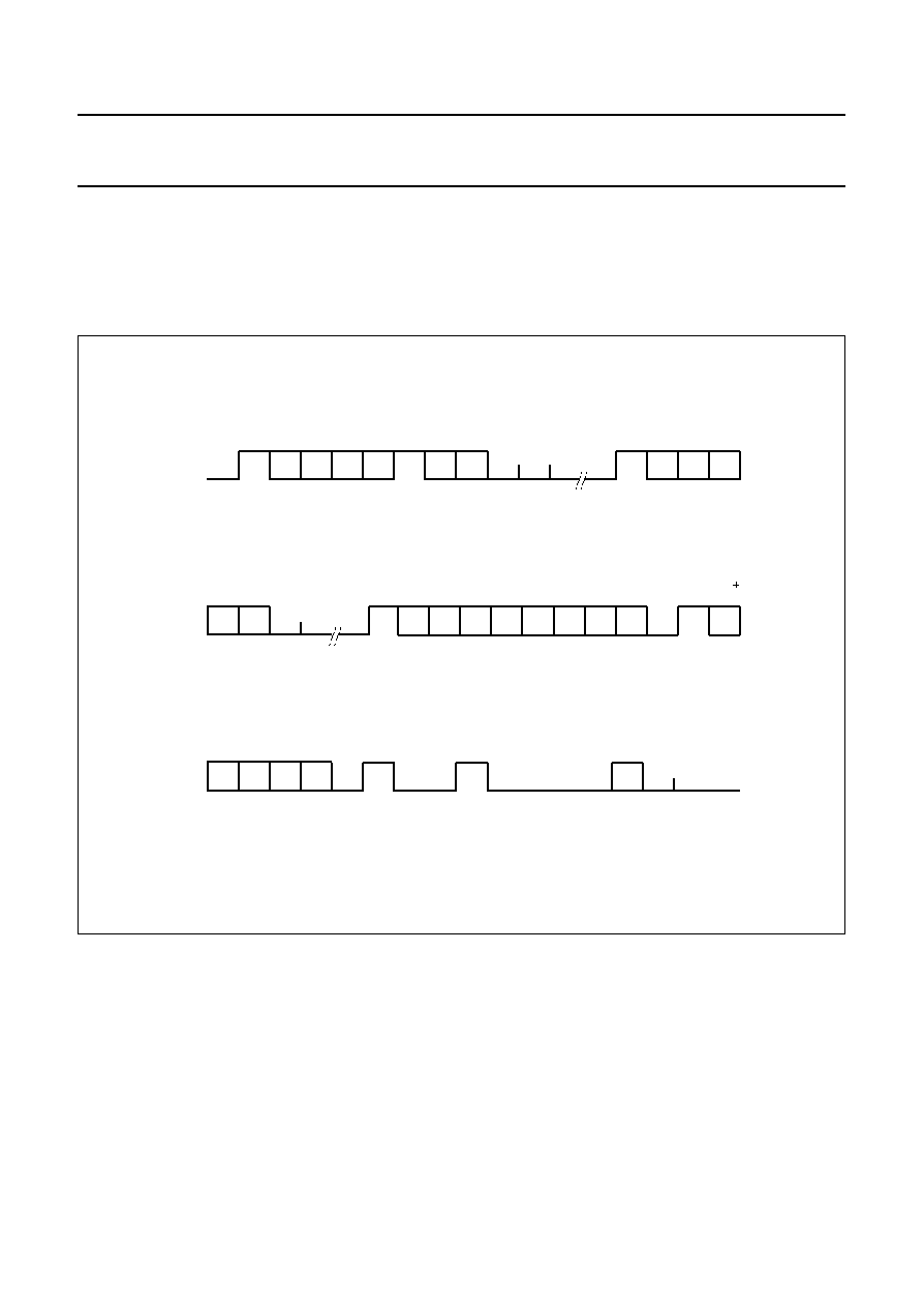
7.14
Call Data output on LED
When enabled by programming of SPF17 = 1, message
data will appear on the LED output OL. The data format
and timing are equal to the signal on DO, except that the
start/stop conditions are replaced with start/stop bits
(respectively 1 and 0). The data format is shown in Fig.16.
No alert signals will appear on OL during message data
transfer. Consecutive message words have a minimum
separation of 1 start bit and 1 stop bit.
Fig.16 Call data transfer on the LED output.
MEA255 - 1
1st message word
address word
OL
START OF TRANSFER
A0
A1
A2
A3
A4
A5
A6
A7
message word N
message word N1
MESSAGE TRANSFER
Mn0 Mn1 Mn2 Mn3 Mn4 Mn5 Mn6 Mn7
termination word
last message word
END OF TRANSFER
T0
T1
T2
T3
T4
T5
T6
T7
start bit
stop bit
start bit
stop bit
start bit
stop bit
start bit
stop bit
start bit
stop bit
message word N 1
OL
OL

1997 Mar 04
21
Philips Semiconductors
Product specification
POCSAG Paging Decoder
PCF5001
7.15
Serial communication call data format
Table 4
Address word format
Table 5
Message word format
Note
1. Bit 7 = 1, if message codeword could not be corrected.
Table 6
Termination word format
Note
1. Bit 7 = 1, if call termination on error.
FUNCTION CODE
CALL ADDRESS
BIT 4
SYNC STATUS
DUPLEX CALL
BIT 7
BIT 0 (LSB)
BIT 1 (MSB)
BIT 2
BIT 3
RIC
BIT 5
BIT 6
Bit 21 of
address
codeword
bit 20 of
address
codeword
0
0
A
1
0 = Data
Receive;
1 = Data fail
1 = Duplex Call
time-out active
0
0
1
B
1
0
C
1
1
D
BIT 0
BIT 1
BIT 2
BIT 3
BIT 4
BIT 5
BIT 6
BIT 7
(1)
LSB
message bits
MSB
error flag
BIT 0
BIT 1
BIT 2
BIT 3
BIT 4
BIT 5
BIT 6
BIT 7
(1)
0
0
1
0
0
0
0
error flag
7.16
Data conversion
The PCF5001 automatically converts message codewords
received in numeric or alphanumeric format into ASCII
format. Depending on SPF13 and the function bit setting in
the received address codeword a conversion takes place
as shown in Table 7.
When a conversion from alphanumeric format to ASCII
takes place, the received message codewords are split
into message blocks, seven bits in length. After adding the
error flag they are transferred as message words.
When a conversion from numeric format to ASCII takes
place, the received message codewords are split into
blocks, four bits in length. Each four bit block is converted
to a seven bit block as shown in Table 8. After adding the
error flag they are transferred as message words.
Table 7
Message data conversion
Note
1. X = don't care.
SPF13
FUNCTION BITS
MESSAGE FORMAT
BIT 20 (MSB)
BIT 21 (LSB)
0
X
(1)
X
(1)
numeric
1
0
0
numeric
1
X
(1)
1
alphanumeric
1
1
X
(1)
alphanumeric

1997 Mar 04
22
Philips Semiconductors
Product specification
POCSAG Paging Decoder
PCF5001
Table 8
Numeric format to ASCII conversion
4-BIT BLOCK
CHARACTER
7-BIT BLOCK
LSB
MSB
LSB
MSB
0
0
0
0
`0'
0
0
0
0
1
1
0
1
0
0
0
`1'
1
0
0
0
1
1
0
0
1
0
0
`2'
0
1
0
0
1
1
0
1
1
0
0
`3'
1
1
0
0
1
1
0
0
0
1
0
`4'
0
0
1
0
1
1
0
1
0
1
0
`5'
1
0
1
0
1
1
0
0
1
1
0
`6'
0
1
1
0
1
1
0
1
1
1
0
`7'
1
1
1
0
1
1
0
0
0
0
1
`8'
0
0
0
1
1
1
0
1
0
0
1
`9'
1
0
0
1
1
1
0
0
1
0
1
`*'
0
1
0
1
0
1
0
1
1
0
1
`U'
1
0
1
0
1
0
1
0
0
1
1
` '
0
0
0
0
0
1
0
1
0
1
1
`
-
'
1
0
1
1
0
1
0
0
1
1
1
`]'
1
0
1
1
1
0
1
1
1
1
1
`['
1
1
0
1
1
0
0
7.17
Memory Organization
The PCF5001 POCSAG decoder contains non-volatile
EEPROM memory to store four user addresses, two frame
numbers and specially programmed function bits (SPF01
to SPF32) for decoder application configuration.
The EEPROM is organized as three arrays of 38 bits each
as shown in Fig.17.
A user address (or RIC) in POCSAG code comprises of
21 bits, but the three least significant bits are coded in the
frame number and therefore not explicitly transmitted. In
the PCF5001, addresses A/B and C/D must share the
same frame number: addresses A and B reside in frame
FR1 (FR10, FR11 and FR12), addresses C and D reside
in frame FR2 (FR20, FR21 and FR22). Figure 18 shows an
example of decimal address to EEPROM content
conversion. Each address must be explicitly enabled by
resetting of the associated enable bit.
1997 Mar 04
23
Philips Semiconductors
Product specification
POCSAG Paging Decoder
PCF5001
Fig.17 EEPROM memory organization.
EEPROM ARRAY 1
B17
B16
B15
B14
B13
B12
B11
B10
B09
B08
B07
B06
B05
B04
B03
B02
B01
B00
A17
A16
A15
A14
A13
A12
A11
A10
A09
A08
A07
A06
A05
A04
A03
A02
A01
A00
BIT18
BIT17 BIT16
BIT15
BIT14
BIT13
BIT12
BIT11 BIT10
BIT9
BIT8
BIT7
BIT6
BIT5
BIT4
BIT3
BIT2
BIT1
BIT0
BIT37
BIT36
BIT35
BIT34 BIT33
BIT32
BIT31
BIT30
BIT29 BIT28
BIT27
BIT26
BIT25
BIT24 BIT23
BIT22
BIT21
BIT20
BIT19
ENA
ENB
C17
C16
C15
C14
C13
C12
C11
C10
C09
C08
C07
C06
C05
C04
C03
C02
C01
C00
D17
D16
D15
D14
D13
D12
D11
D10
D09
D08
D07
D06
D05
D04
D03
D02
D01
D00
EEPROM ARRAY 2
BIT18
BIT17 BIT16
BIT15
BIT14
BIT13
BIT12
BIT11 BIT10
BIT9
BIT8
BIT7
BIT6
BIT5
BIT4
BIT3
BIT2
BIT1
BIT0
BIT37
BIT36
BIT35
BIT34 BIT33
BIT32
BIT31
BIT30
BIT29 BIT28
BIT27
BIT26
BIT25
BIT24 BIT23
BIT22
BIT21
BIT20
BIT19
___
ENC
END
SPF13 SPF12 SPF11 SPF10 SPF09 SPF08 SPF07 SPF06 SPF05 SPF04 SPF03 SPF02 SPF01 FR20
FR21
FR22
FR10
FR11
FR12
SPF32 SPF31 SPF30 SPF29 SPF28 SPF27 SPF26 SPF25 SPF24 SPF23 SPF22 SPF21 SPF20 SPF19 SPF18 SPF17 SPF16
SPF14
EEPROM ARRAY 3
BIT18
BIT17 BIT16
BIT15
BIT14
BIT13
BIT12
BIT11 BIT10
BIT9
BIT8
BIT7
BIT6
BIT5
BIT4
BIT3
BIT2
BIT1
BIT0
BIT37
BIT36
BIT35
BIT34 BIT33
BIT32
BIT31
BIT30
BIT29 BIT28
BIT27
BIT26
BIT25
BIT24 BIT23
BIT22
BIT21
BIT20
BIT19
SPF15
MCD469
A00 represents the MSB of RIC A, B00 is the MSB of RIC C, etc.
FR10 represents the MSB of Frame 1 (valid for RICs A and B), FR20 is the MSB of Frame 2 (RICs C and D).

1997 Mar 04
24
Philips Semiconductors
Product specification
POCSAG Paging Decoder
PCF5001
7.18
Description of the Special Programmed Function (SPF) bits
The following features can be selected by appropriate programming of the special programmed function bits as shown
in Table 9.
Table 9
Special Programmed Function (SPF) bits
SPF
BIT
FUNCTION
SPF01
0
Alert-only pager mode.
1
Display pager mode.
SPF02
0
512 bits/s data rate.
1
1200 bits/s data rate, possible with 76.8 kHz crystal only.
SPF03
0
32768 Hz crystal configuration.
1
76800 Hz crystal configuration.
SPF04, SPF05
Receiver establishment time (depending on data rate).
00
7.8 ms/512 bits/s; 53.3 ms/1200 bits/s.
01
15.6 ms/512 bits/s; 6.7 ms/1200 bits/s.
10
31.3 ms/512 bits/s; 13.3 ms/1200 bits/s.
11
62.5 ms/512 bits/s; 26.7 ms/1200 bits/s.
Fig.18 Decimal address to memory contents conversion example.
A00 is the MSB of RIC A, FR10 is the MSB of Frame 1.
MCD470
0
0
0
0
0
0
0
1
1
0
0
0
0
1
0
1
1
0
EEPROM Allocation
binary equivalent (18 + 3 bit available)
000000011000010110100
address decimal value
(example: RIC A)
RIC A = 1 2 4 6 8
A00
A01
A02
A03
A04
A05
A06
A07
A08
A09
A10
A11
A12
A13
A14
A15
A16
A17
1
0
0
FR10 FR11 FR12

1997 Mar 04
25
Philips Semiconductors
Product specification
POCSAG Paging Decoder
PCF5001
Note
1. Call termination on:
a) First codeword immediately following address codeword uncorrectable.
b) Two consecutive codewords uncorrectable.
SPF06, SPF07
Duplicate call suppression time-out and out-of-range hold-off time-out.
00
30 s.
01
60 s.
10
120 s.
11
240 s.
SPF08
0
Voltage converter disabled, if SPF01 = 1 (`display pager' mode).
1
Voltage converter enabled, if SPF01 = 1 (`display pager' mode).
SPF09
0
SILENT override on address C disabled.
1
SILENT override on address C enabled.
SPF10
0
SILENT override on address D disabled.
1
SILENT override on address D enabled.
SPF11
0
Vibrator output disabled.
1
Vibrator output enabled.
SPF12
0
Call termination criteria combination method (note 1).
1
Call termination criteria defined by SPF13.
SPF13
0
Numeric data deformatting, call termination on first uncorrectable codeword.
1
Numeric data deformatting on function code 00 only, call termination on two
uncorrectable codewords.
SPF14
0
Duplicate call suppression disabled.
1
Duplicate call suppression enabled.
SPF15
0
Out of range indication at OL output disabled, hold-off period is zero regardless
of SPF06 and SPF07 setting.
1
Out of range indication at OL output enabled, hold-off period is according to
SPF06 and SPF07 setting.
SPF16
0
Repeat alert disabled.
1
Repeat alert enabled.
SPF17
0
Call data output on OL disabled.
1
Call data output on OL enabled.
SPF18
-
Spare.
SPF19
-
Program always 0.
SPF20 to SPF30
-
Spares.
SPF31
0
Alerter frequency 2048 Hz.
1
Alerter frequency 2731 Hz.
SPF32
0
Frequency reference output 16384 Hz if SPF01 = 1 (`display pager' mode).
1
Frequency reference output 32768 Hz if SPF01 = 1 (`display pager' mode).
SPF
BIT
FUNCTION

1997 Mar 04
26
Philips Semiconductors
Product specification
POCSAG Paging Decoder
PCF5001
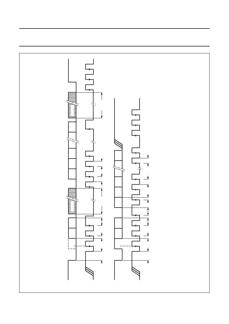
7.19
EEPROM Write operation
The program mode is entered in OFF status by setting the
PD input LOW and the PS input HIGH at any time.
The `program' mode is left and normal operation resumed
by either removing the power supply or setting the PD
input HIGH after the 38
th
data bit while continuing to clock
the PS input. The three EEPROM arrays can be
programmed in any order. Selection of array is made
during the second and third pulse on the PS input.
The `program' mode has to be left after programming of
each array.
After entering the `program' mode, keeping input PD LOW
during the first pulse on PS selects Memory Write
operation. After selection of the current array an erase
cycle of duration t
PEW
has to be carried out, during which
the supply voltage at V
SS
input must be at least V
PG
.
Program data for the selected array is entered bit by bit
using PD as data input and the rising edge on PS as data
strobe pulse. See Fig.19 for timing during an EEPROM
write operation.
After the last bit a special write cycle of duration t
PEW
has
to be carried out again, during which the supply voltage at
V
SS
input must be V
PG
. During conditions when the supply
voltage is increased to V
PG
the maximum DC ratings at V
ref
must not be exceeded. When the on-chip voltage
converter is enabled a voltage regulator diode or a
damping resistor of sufficiently low impedance has to be
connected between V
ref
and V
SS
to limit the voltage level
at V
ref
during program operation.
7.20
EEPROM Read operation
After entrance to the `program' mode, keeping input PD
HIGH during the first pulse on PS selects Memory Read
operation. After selection of the current array the
programmed data is output bit-by-bit using PD as data
output. A positive edge on PS input switches to the next
bit. See Fig.19 for timing during an EEPROM read
operation.
7.21
Read-back operation via Microcontroller
Interface
In `display pager' mode, the PCF5001 is capable of
delivering the EEPROM contents to an external
microcontroller using the serial interface outputs DO and
DS. The EEPROM data transfer mode is selected by
applying a LOW to input ON and a HIGH to input SK while
pulsing the SR input, and the interface is enabled (IE is
HIGH). The data transfer is started by a logic HIGH level
on SR. The HIGH level on SR must be removed before the
end of the tenth output byte, otherwise the transfer is
aborted and restarted. The minimum pulse duration
corresponds with t
SPD
in the status interrogation timing
(see Fig.7). The transfer is organized as 15-byte transfers.
The contents of each array are extended to 40 bits by
trailing zeros. The EEPROM data transfer starts with array
1, bit 0. A valid data bit at DO is indicated by a LOW-level
on DS as shown in Fig.20.
During EEPROM Read-back operation, the PCF5001
configuration and the outputs FL, OL are undefined.
After completion of the Read-Back operation, the
PCF5001 will re-enter the programmed configuration.
7.22
Voltage converter
The PCF5001 contains a switched capacitor-type on-chip
voltage converter, which can provide doubled supply
voltage to the external microcontroller and display control
devices. The microcontroller interface signals are level
shifted accordingly.
A capacitor of 100 nF (C
S
) must be connected between
pins CP and CN while a load capacitor of 10
µ
F is
connected to V
ref
as shown in Fig.23. The voltage
converter operates in `display pager' mode only, when
enabled by programming SPF08 (see Table 9).
1997 Mar 04
27
Philips Semiconductors
Product specification
POCSAG Paging Decoder
PCF5001
MCD471 - 2
WRITE
SEL0
SEL1
1.5 MHz
1.5 MHz
1
23
456
7
4
2
4
3
4
4
4
5
t
PEW
t
PCL
t PCH
t
PEW
t PDH
t
PSI
t RES
PD
PS
12
t RES
PD
PS
READ
SEL0
SEL1
BIT0
BIT1
BIT2
BIT37
34
56
7
4
1
4
2
4
3
4
4
4
5
t PCL
t PCH
t PDH
t
PSI
t
PSO
t PRS
BIT0
BIT1
BIT2
BIT37
Fig.19 EEPROM read/write timing.

1997 Mar 04
28
Philips Semiconductors
Product specification
POCSAG Paging Decoder
PCF5001
Fig.20 EEPROM data transfer to microcontroller timing.
B17
D17
FR12
SR
DO
DS
SPF
32
MCD472
ENC
ENA
t SDD
t DSE
7.23
Test modes of the decoder
The decoder supports two test modes, which are intended
for use during pager production and type approval tests.
7.23.1
B
OARD TEST MODE
`Board test' mode is selected by setting the PD input LOW
at any time. In this test mode the following features are
provided:
1. Receiver enable output is set constantly HIGH
2. Output AL is activated by a LOW-level on ON input
3. Output AH is activated by a HIGH-level on SR input
4. Outputs OL and OM are activated by a HIGH-level on
SK input.
Exit from `board test' mode is achieved by setting input PD
HIGH.
7.23.2
P
AGER
T
EST
M
ODE
(T
YPE
A
PPROVAL
M
ODE
)
`Pager test' mode is entered by reception of a valid call
while `board test' mode is active, see above. In `pager test'
mode:
1. Call alert cadences are terminated after 2 seconds
2. Duplicate call suppression is disabled.
Exit from `pager test' mode is achieved by disconnecting
the power supply from the decoder.

1997 Mar 04
29
Philips Semiconductors
Product specification
POCSAG Paging Decoder
PCF5001
8
LIMITING VALUES
In accordance with the Absolute Maximum Rating System (IEC 134).
Note
1. V
DD
is connected to the substrate (see Fig.1), and is referred to as common, 0 V.
9
DC CHARACTERISTICS
V
DD
= 0 V; V
SS
=
-
2.7 V; V
ref
= 2.7 V; T
amb
= 25
°
C; unless otherwise specified.
Quartz crystal parameters: f = 76800 Hz; R
S(max)
= 40 k
; C
L
= 12 pF.
Decoder Mode programmed as Alert-only (SPF01 = 0).
SYMBOL
PARAMETER
CONDITIONS
MIN.
MAX.
UNIT
V
SS
supply voltage
note 1
+0.5
-
8.0
V
V
PG
programming supply voltage
-
5.5
-
V
V
n
voltage on pins FL, DS, DO, OR, BL,
AI, ON, SK, SR and IE
+0.8
V
ref
-
0.8
V
V
n1
input voltage on any other pin
+0.8
V
SS
-
0.8
V
P
tot
total power dissipation
-
250
mW
P
O
power dissipation per output
-
100
mW
I
I(max)
maximum input current (any input)
-
10
mA
I
O(max)
maximum output current
any output except AL
-
20
mA
output AL
-
70
mA
T
amb
operating ambient temperature
-
40
+85
°
C
T
stg
storage temperature
-
55
+125
°
C
SYMBOL
PARAMETER
CONDITIONS
MIN.
TYP.
MAX.
UNIT
Supply
V
SS
supply voltage
voltage converter disabled;
all outputs open-circuit
T
amb
=
-
10 to +85
°
C
-
1.5
-
2.7
-
6.0
V
T
amb
=
-
40 to +85
°
C
-
1.8
-
2.7
-
6.0
V
I
SS
supply current
note 1
-
-
60
-
100
µ
A
V
PG
programming supply voltage
note 2
-
4.5
-
5.0
-
5.5
V
I
PG
programming supply current
-
-
500
-
µ
A

1997 Mar 04
30
Philips Semiconductors
Product specification
POCSAG Paging Decoder
PCF5001
Notes
1. All inputs = V
SS
; voltage converter off; all outputs open-circuit.
2. See Section 7.19 and Chapter 8 for limitations of V
ref
when programming while the voltage converter is enabled.
Inputs
V
IL1
LOW level input voltage
PD, PS, DI, BS, TS, TT and X1
0.7V
SS
-
-
V
V
IL2
LOW level input voltage AI, ON,
SR, SK and IE
0.7V
ref
-
-
V
V
IH1
HIGH level input voltage
PD, PS, DI, BS, TS, TT and X1
-
-
0.3V
SS
V
V
IH2
HIGH level input voltage
AI, ON, SR, SK and IE
-
-
0.3V
ref
V
I
I
input current
BS, PS, TS and TT
V
I
= V
DD
7.0
-
20.0
µ
A
PD
V
I
= V
SS
-
9.0
-
-
24.0
µ
A
DI
V
I
= V
DD
; RE = 0
7.0
-
20.0
µ
A
DI
V
I
= V
DD
; RE = 1
0
-
0.5
µ
A
ON and SK
V
I
= V
SS
-
0.5
-
0.8
-
1.1
µ
A
AI and SR
V
I
= V
DD
7.0
-
20.0
µ
A
C
i
input capacitance BS, DI, PD,
PS, TS, TT, AI, ON, SR, SK, IE
and X1
2
-
-
pF
Outputs
I
OL
LOW level output current
OL, OM and AH
V
OL
=
-
1.35 V
100
-
-
µ
A
DO, DS, BL, FL and OR
V
OL
=
-
1.35 V
100
-
-
µ
A
AL
V
OL
=
-
1.5 V
17.5
-
-
mA
RE
V
OL
= 2.2 V
200
-
-
µ
A
I
OH
HIGH level output current
OL, OM and AH
V
OH
=
-
1.35 V
-
0.8
-
-
1.8
mA
DO, DS, BL, FL and OR
V
OH
=
-
1.35 V
-
100
-
-
µ
A
AL
AL high-impedance
-
-
-
0.2
µ
A
RE
V
OH
=
-
0.5 V
-
1.0
-
-
mA
Oscillator
C
XO
output capacitance X2
-
40
-
pF
g
m
oscillator transconductance
V
SS
=
-
1.5 V
15
29
43
µ
S
V
SS
=
-
6.0 V
25
39
55
µ
S
V
PU
power-up reset threshold
voltage
-
-
1.2
-
V
SYMBOL
PARAMETER
CONDITIONS
MIN.
TYP.
MAX.
UNIT
1997 Mar 04
31
Philips Semiconductors
Product specification
POCSAG Paging Decoder
PCF5001
10 DC CHARACTERISTICS (WITH VOLTAGE CONVERTER)
V
DD
= 0 V; V
SS
=
-
3.0 V; V
ref
=
-
6.0 V; T
amb
= 25
°
C.
Quartz crystal parameters: f = 76800 Hz; R
S(max)
= 40 k
; C
L
= 12 pF.
Decoder Mode programmed as Display Pager (SPF01 = 1).
Voltage converter enabled (SPF08 = 1); C
S
= 100 nF.
11 AC CHARACTERISTICS
V
DD
= 0 V; V
SS
=
-
2.7 V; T
amb
= 25
°
C.
Quartz crystal parameters: f = 32768 or 76800 Hz; R
S(max)
= 40 k
; C
L
= 12 pF.
Decoder Mode programmed as Display or Alert-only Pager (SPF01 = 1 or 0).
SYMBOL
PARAMETER
CONDITIONS
MIN.
TYP.
MAX.
UNIT
Supply
V
SS
supply voltage
-
1.5
-
-
3.0
V
Voltage converter
V
ref(0)
output voltage; no load
V
SS
=
-
3.0 V
-
5.8
-
-
6.0
V
V
ref
output voltage
V
SS
=
-
2.0 V; I
ref
= 250
µ
A
-
3.0
-
3.5
-
V
I
ref
output current
V
SS
=
-
2.0 V; V
ref
=
-
2.7 V
400
600
-
µ
A
V
SS
=
-
3.0 V; V
ref
=
-
4.5 V
600
900
-
µ
A
Inputs
I
I
input current
AI, ON, SR and SK
V
I
= V
ref
-
0
-
0.5
µ
A
ON and SK
V
I
= V
DD
-
0
±
0.5
µ
A
SR
V
I
= V
DD
; V
ref
=
-
6.0 V
-
17
-
µ
A
SYMBOL
PARAMETER
CONDITIONS
MIN.
TYP.
MAX.
UNIT
Alert frequency
f
AL
alert frequency
SPF31 = 0
-
2048
-
Hz
f
AWH
high alert warble frequency
-
1024
-
Hz
f
AWL
low alert warble frequency
-
16
-
Hz
f
AL
alert frequency
SPF31 = 1
-
2731
-
Hz
f
AWH
high alert warble frequency
-
1365
-
Hz
f
AWL
low alert warble frequency
-
16
-
Hz
f
FL
output frequency reference at FL
SPF32 = 0
-
16384
-
Hz
SPF32 = 1
-
32768
-
Hz

1997 Mar 04
32
Philips Semiconductors
Product specification
POCSAG Paging Decoder
PCF5001
Call alert duration
t
ALT
time-out period
-
16
-
s
t
ALL
alert time LOW (AL output only)
-
4
-
s
t
ALH
alert time HIGH (AH and AL outputs)
-
12
-
s
t
ALC
call alert cycle time
see Fig.9
-
1
-
s
t
ALP
call alert pulse duration
see Fig.9
-
125
-
ms
t
ALD
call alert hold off period
see Fig.8
52
-
-
ms
t
RPT
repeat alert duration
see Fig.11
-
-
4
s
t
RCR
repeat alert recurrence time
see Fig.11
-
-
15
s
t
RCP
repeat alert cycle time
-
-
500
ms
t
RPD
repeat alert pulse duration
-
-
250
ms
t
STON
status alert time
see Fig.10
-
-
62.5
ms
t
STOF
status alert delay
see Fig.10
-
-
62.5
ms
t
SUA
start-up alert time
SPF02 = 0; see Fig.13
-
-
500
ms
SPF02 = 1; see Fig.13
-
-
453
ms
t
ORA
out-of-range alert pulse width
see Fig.12
-
-
62.5
ms
t
ORD
out-of-range alert time
see Fig.12
-
-
2
s
t
BLAL
battery LOW-level alert time
-
-
16
s
Receiver control
t
RXT
RE transition time
C
L
= 5 pF
-
-
100
ns
t
RXON
RE establishment time
SPF04 = 0; SPF05 = 1
-
7.8
62.5
ms
Data output
f
DO
data output rate
-
2048
-
bits/s
t
DSD
strobe period call data
see Fig.15
480
-
495
µ
s
t
DSE
strobe period EEPROM data
see Fig.20
200
488
1150
µ
s
t
DSW
data strobe pulse width
see Fig.15
230
-
250
µ
s
t
TDO
data output transition time
C
L
= 10 pF; see Fig.15
-
-
100
ns
t
DOS
data output set-up time
see Fig.15
-
-
135
µ
s
t
DOH
data output hold time
see Fig.15
115
-
-
µ
s
t
BYD
consecutive byte delay
1210
-
1225
µ
s
t
CWD
inter-codeword delay
1200 bits/s numeric message
3420
-
-
µ
s
t
ST
start condition set-up time
see Fig.15
4750
-
-
µ
s
t
SP
stop condition set-up time
see Fig.15
595
-
615
µ
s
t
STL
start bit period OL output
480
-
495
µ
s
t
SPL
stop bit period OL output
480
488
495
µ
s
t
SDD
SPF output delay
see Fig.20
1
-
10
ms
SYMBOL
PARAMETER
CONDITIONS
MIN.
TYP.
MAX.
UNIT

1997 Mar 04
33
Philips Semiconductors
Product specification
POCSAG Paging Decoder
PCF5001
12 TIMING CHARACTERISTICS
V
DD
= 0 V; V
SS
=
-
2.7 V; T
amb
= 25
°
C.
Quartz crystal parameters: f = 32768 or 76800 Hz; R
S(max)
= 40 k
; C
L
= 12 pF.
Decoder Mode programmed as Display or Alert-only Pager (SPF01 = 1 or 0).
SYMBOL
PARAMETER
CONDITIONS
MIN.
TYP.
MAX.
UNIT
Operating frequency dependent
f
osc
oscillator frequency
SPF03 = 0
-
32768
-
Hz
SPF03 = 1
-
76800
-
Hz
t
TDI
data input transition time
see Fig.21
-
-
100
µ
s
t
DI1
data input logic 1
see Fig.21
t
BIT
-
t
DI0
data input logic 0
see Fig.21
t
BIT
-
f
DI
data input rate
SPF02 = 0
-
512
-
bits/s
t
BIT
bit period
-
1.9531
-
ms
t
CW
codeword duration
-
62.5
-
ms
t
PA
preamble duration
1125
-
-
ms
t
BAT
batch duration
-
1062.5
-
ms
f
DI
data input rate
SPF02 = 1; f
osc
= 76800 Hz
-
1200
-
bits/s
t
BIT
bit period
-
833.3
-
ms
t
CW
codeword duration
-
26.7
-
ms
t
PA
preamble duration
480
-
-
ms
t
BAT
batch duration
-
453.3
-
ms
Alert only mode (SPF01 = 0)
t
SDB
switch debounce period
-
62.5
-
ms
Display pager mode (SPF01 = 1); see Figs 6 and 7
t
STP
status set-up time
f
osc
= 32768 Hz
35
-
-
µ
s
t
STD
status change delay
-
-
35
µ
s
t
IEH
interface enable hold time
35
-
-
µ
s
t
STH
status hold time
35
-
-
µ
s
t
SPD
status pulse duration
35
-
-
µ
s
t
STP
status set-up time
f
osc
= 76800 Hz
15
-
-
µ
s
t
STD
status change delay
-
-
15
µ
s
t
IEH
interface enable hold time
15
-
-
µ
s
t
STH
status hold time
15
-
-
µ
s
t
SPD
status pulse duration
15
-
-
µ
s
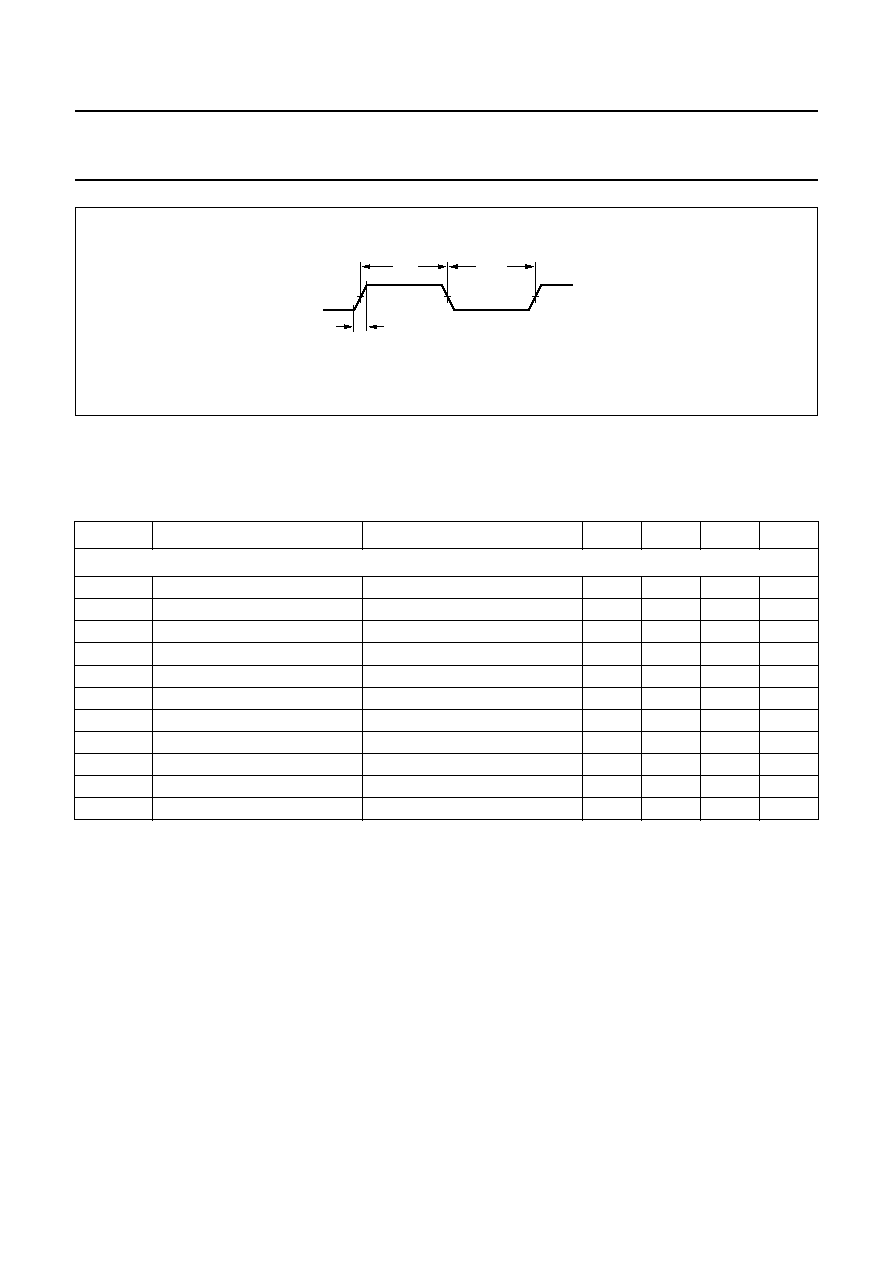
1997 Mar 04
34
Philips Semiconductors
Product specification
POCSAG Paging Decoder
PCF5001
13 PROGRAMMING CHARACTERISTICS
V
DD
= 0 V; V
SS
= V
PG
=
-
5.0 V (see notes 1, 2 and 3); V
ref
= V
SS
; pins 2 and 3 open-circuit; T
amb
= 25
°
C.
Quartz crystal parameters: f = 32768 Hz; R
S(max)
= 40 k
; C
L
= 12 pF.
Decoder in OFF status.
Notes
1. V
SS
= V
PG
only required during erase/write (t
PEW
in Fig.19), otherwise V
SS(min)
=
-
1.5 V.
2. Maximum voltage for programming (V
PG
) is
-
5.5 V.
3. See Section 7.19 and Chapter 8 for limitations of V
ref
when programming while the voltage converter is enabled.
4. EEPROM programming is also possible at higher frequencies (76.8 kHz or 153.6 kHz). The timings shown then
become proportionally smaller.
SYMBOL
PARAMETER
CONDITIONS
MIN.
TYP.
MAX.
UNIT
Programming; see Fig.19
t
RES
power-up reset pulse width
note 4
35
-
-
µ
s
t
PEW
erase/write time
10
-
-
ms
f
EW
erase/write frequency
1.0
1.5
2.0
MHz
t
EW
erase/write cycles
1000
10000
-
-
t
DR
data retention time
T
amb
= 85
°
C
10
-
-
years
t
PCH
data clock HIGH time
note 4
65
-
-
µ
s
t
PCL
data clock LOW time
note 4
65
-
-
µ
s
t
PRS
read set-up time
note 4
-
-
35
µ
s
t
PSI
data set-up time on input
note 4
35
-
-
µ
s
t
PSO
data set-up time on output
note 4
-
-
35
µ
s
t
PDH
data hold time
note 4
35
-
-
µ
s
handbook, halfpage
MGL100
tDI1
tDI0
t
TDI
Fig.21 Data input timing.
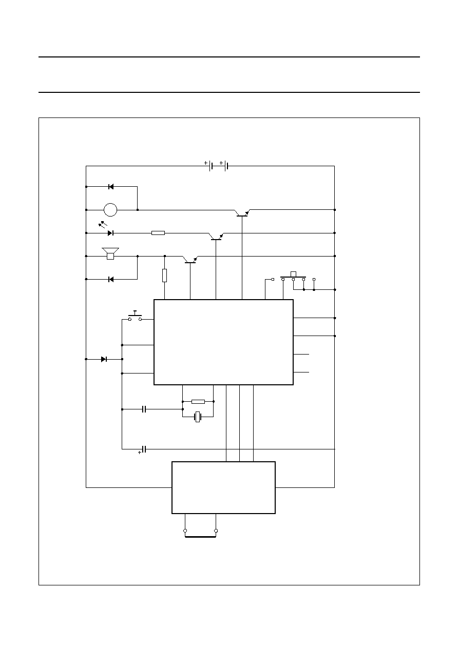
1997 Mar 04
35
Philips Semiconductors
Product specification
POCSAG Paging Decoder
PCF5001
14 APPLICATION INFORMATION
X1
V
DD
X2
BS
PCF5001
DI
RE
PD
V
SS
OM
PS
OL
V
REF
ON
SR
SK
IE
AL
AH
M
10 pF
32768 Hz
or
76800 Hz
data output
Rx control
battery low
indicator
RECEIVER
antenna
V
CC
V
EE
1.5V
1.5V
MLB046
status
reset
OFF
ON
SIL
Fig.22 Alert-only pager application example.

1997 Mar 04
36
Philips Semiconductors
Product specification
POCSAG Paging Decoder
PCF5001
X1
V
DD
V
SS
V
DD
X2
BS
PCF5001
DI
RE
CN
CP
PD
V
SS
OM
PS
OL
V
REF
FL
DS
DO
OR
BL
AI
ON
SR
SK
IE
AL
AH
M
1.5V
1.5V
switch matrix
MICRO
CONTROLLER
10 pF
32768 Hz
or
76800 Hz
data output
Rx control
battery low
indicator
RECEIVER
antenna
100 nF
LCD
V
CC
V
EE
MLB047
C
S
10 F
µ
Fig.23 Display-pager application example.
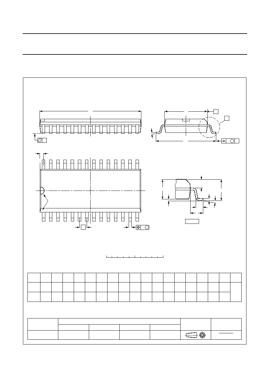
1997 Mar 04
37
Philips Semiconductors
Product specification
POCSAG Paging Decoder
PCF5001
15 PACKAGE OUTLINES
UNIT
A
max.
A
1
A
2
A
3
b
p
c
D
(1)
E
(1)
(1)
e
H
E
L
L
p
Q
Z
y
w
v
REFERENCES
OUTLINE
VERSION
EUROPEAN
PROJECTION
ISSUE DATE
IEC
JEDEC
EIAJ
mm
inches
2.65
0.30
0.10
2.45
2.25
0.49
0.36
0.32
0.23
18.1
17.7
7.6
7.4
1.27
10.65
10.00
1.1
1.0
0.9
0.4
8
0
o
o
0.25
0.1
DIMENSIONS (inch dimensions are derived from the original mm dimensions)
Note
1. Plastic or metal protrusions of 0.15 mm maximum per side are not included.
1.1
0.4
SOT136-1
91-08-13
95-01-24
X
14
28
w
M
A
A
1
A
2
b
p
D
H
E
L
p
Q
detail X
E
Z
c
L
v
M
A
e
15
1
(A )
3
A
y
0.25
075E06
MS-013AE
pin 1 index
0.10
0.012
0.004
0.096
0.089
0.019
0.014
0.013
0.009
0.71
0.69
0.30
0.29
0.050
1.4
0.055
0.42
0.39
0.043
0.039
0.035
0.016
0.01
0.25
0.01
0.004
0.043
0.016
0.01
0
5
10 mm
scale
SO28: plastic small outline package; 28 leads; body width 7.5 mm
SOT136-1
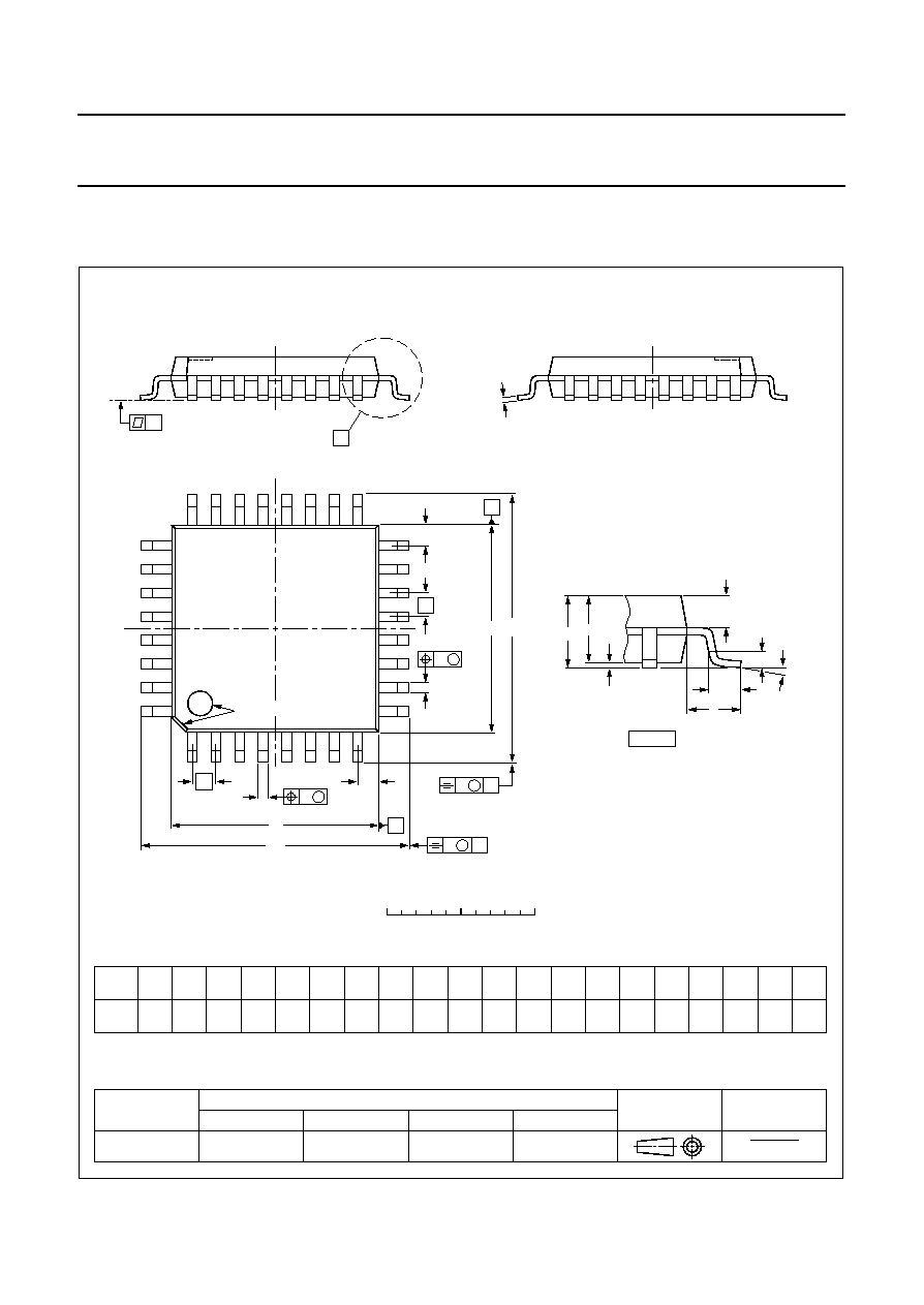
1997 Mar 04
38
Philips Semiconductors
Product specification
POCSAG Paging Decoder
PCF5001
UNIT
A
max.
A
1
A
2
A
3
b
p
c
E
(1)
e
H
E
L
L
p
Q
Z
y
w
v
REFERENCES
OUTLINE
VERSION
EUROPEAN
PROJECTION
ISSUE DATE
IEC
JEDEC
EIAJ
mm
1.60
0.20
0.05
1.45
1.35
0.25
0.4
0.3
0.18
0.12
7.1
6.9
0.8
9.15
8.85
0.69
0.59
0.9
0.5
7
0
o
o
0.25
0.1
1.0
0.2
DIMENSIONS (mm are the original dimensions)
Note
1. Plastic or metal protrusions of 0.25 mm maximum per side are not included.
0.75
0.45
SOT358 -1
93-06-29
95-12-19
D
(1)
(1)
(1)
7.1
6.9
H
D
9.15
8.85
E
Z
0.9
0.5
D
b
p
e
E
A
1
A
L
p
Q
detail X
L
(A )
3
B
8
c
D
H
b
p
E
H
A
2
v
M
B
D
Z D
A
Z E
e
v
M
A
X
1
32
25
24
17
16
9
y
pin 1 index
w
M
w
M
0
2.5
5 mm
scale
LQFP32: plastic low profile quad flat package; 32 leads; body 7 x 7 x 1.4 mm
SOT358-1

1997 Mar 04
39
Philips Semiconductors
Product specification
POCSAG Paging Decoder
PCF5001
16 SOLDERING
16.1
Introduction
There is no soldering method that is ideal for all IC
packages. Wave soldering is often preferred when
through-hole and surface mounted components are mixed
on one printed-circuit board. However, wave soldering is
not always suitable for surface mounted ICs, or for
printed-circuits with high population densities. In these
situations reflow soldering is often used.
This text gives a very brief insight to a complex technology.
A more in-depth account of soldering ICs can be found in
our
"IC Package Databook" (order code 9398 652 90011).
16.2
Reflow soldering
Reflow soldering techniques are suitable for all LQFP and
SO packages.
Reflow soldering requires solder paste (a suspension of
fine solder particles, flux and binding agent) to be applied
to the printed-circuit board by screen printing, stencilling or
pressure-syringe dispensing before package placement.
Several techniques exist for reflowing; for example,
thermal conduction by heated belt. Dwell times vary
between 50 and 300 seconds depending on heating
method. Typical reflow temperatures range from
215 to 250
°
C.
Preheating is necessary to dry the paste and evaporate
the binding agent. Preheating duration: 45 minutes at
45
°
C.
16.3
Wave soldering
16.3.1
LQFP
Wave soldering is not recommended for LQFP packages.
This is because of the likelihood of solder bridging due to
closely-spaced leads and the possibility of incomplete
solder penetration in multi-lead devices.
If wave soldering cannot be avoided, the following
conditions must be observed:
·
A double-wave (a turbulent wave with high upward
pressure followed by a smooth laminar wave)
soldering technique should be used.
·
The footprint must be at an angle of 45
°
to the board
direction and must incorporate solder thieves
downstream and at the side corners.
Even with these conditions, do not consider wave
soldering LQFP packages LQFP48 (SOT313-2),
LQFP64 (SOT314-2) or LQFP80 (SOT315-1).
16.3.2
SO
Wave soldering techniques can be used for all SO
packages if the following conditions are observed:
·
A double-wave (a turbulent wave with high upward
pressure followed by a smooth laminar wave) soldering
technique should be used.
·
The longitudinal axis of the package footprint must be
parallel to the solder flow.
·
The package footprint must incorporate solder thieves at
the downstream end.
16.3.3
M
ETHOD
(LQFP
AND
SO)
During placement and before soldering, the package must
be fixed with a droplet of adhesive. The adhesive can be
applied by screen printing, pin transfer or syringe
dispensing. The package can be soldered after the
adhesive is cured.
Maximum permissible solder temperature is 260
°
C, and
maximum duration of package immersion in solder is
10 seconds, if cooled to less than 150
°
C within
6 seconds. Typical dwell time is 4 seconds at 250
°
C.
A mildly-activated flux will eliminate the need for removal
of corrosive residues in most applications.
16.4
Repairing soldered joints
Fix the component by first soldering two diagonally-
opposite end leads. Use only a low voltage soldering iron
(less than 24 V) applied to the flat part of the lead. Contact
time must be limited to 10 seconds at up to 300
°
C. When
using a dedicated tool, all other leads can be soldered in
one operation within 2 to 5 seconds between
270 and 320
°
C.

1997 Mar 04
40
Philips Semiconductors
Product specification
POCSAG Paging Decoder
PCF5001
17 DEFINITIONS
18 LIFE SUPPORT APPLICATIONS
These products are not designed for use in life support appliances, devices, or systems where malfunction of these
products can reasonably be expected to result in personal injury. Philips customers using or selling these products for
use in such applications do so at their own risk and agree to fully indemnify Philips for any damages resulting from such
improper use or sale.
Data sheet status
Objective specification
This data sheet contains target or goal specifications for product development.
Preliminary specification
This data sheet contains preliminary data; supplementary data may be published later.
Product specification
This data sheet contains final product specifications.
Limiting values
Limiting values given are in accordance with the Absolute Maximum Rating System (IEC 134). Stress above one or
more of the limiting values may cause permanent damage to the device. These are stress ratings only and operation
of the device at these or at any other conditions above those given in the Characteristics sections of the specification
is not implied. Exposure to limiting values for extended periods may affect device reliability.
Application information
Where application information is given, it is advisory and does not form part of the specification.

1997 Mar 04
41
Philips Semiconductors
Product specification
POCSAG Paging Decoder
PCF5001
NOTES

1997 Mar 04
42
Philips Semiconductors
Product specification
POCSAG Paging Decoder
PCF5001
NOTES

1997 Mar 04
43
Philips Semiconductors
Product specification
POCSAG Paging Decoder
PCF5001
NOTES

Internet: http://www.semiconductors.philips.com
Philips Semiconductors a worldwide company
© Philips Electronics N.V. 1997
SCA53
All rights are reserved. Reproduction in whole or in part is prohibited without the prior written consent of the copyright owner.
The information presented in this document does not form part of any quotation or contract, is believed to be accurate and reliable and may be changed
without notice. No liability will be accepted by the publisher for any consequence of its use. Publication thereof does not convey nor imply any license
under patent- or other industrial or intellectual property rights.
Netherlands: Postbus 90050, 5600 PB EINDHOVEN, Bldg. VB,
Tel. +31 40 27 82785, Fax. +31 40 27 88399
New Zealand: 2 Wagener Place, C.P.O. Box 1041, AUCKLAND,
Tel. +64 9 849 4160, Fax. +64 9 849 7811
Norway: Box 1, Manglerud 0612, OSLO,
Tel. +47 22 74 8000, Fax. +47 22 74 8341
Philippines: Philips Semiconductors Philippines Inc.,
106 Valero St. Salcedo Village, P.O. Box 2108 MCC, MAKATI,
Metro MANILA, Tel. +63 2 816 6380, Fax. +63 2 817 3474
Poland: Ul. Lukiska 10, PL 04-123 WARSZAWA,
Tel. +48 22 612 2831, Fax. +48 22 612 2327
Portugal: see Spain
Romania: see Italy
Russia: Philips Russia, Ul. Usatcheva 35A, 119048 MOSCOW,
Tel. +7 095 755 6918, Fax. +7 095 755 6919
Singapore: Lorong 1, Toa Payoh, SINGAPORE 1231,
Tel. +65 350 2538, Fax. +65 251 6500
Slovakia: see Austria
Slovenia: see Italy
South Africa: S.A. PHILIPS Pty Ltd., 195-215 Main Road Martindale,
2092 JOHANNESBURG, P.O. Box 7430 Johannesburg 2000,
Tel. +27 11 470 5911, Fax. +27 11 470 5494
South America: Rua do Rocio 220, 5th floor, Suite 51,
04552-903 Săo Paulo, SĂO PAULO - SP, Brazil,
Tel. +55 11 821 2333, Fax. +55 11 829 1849
Spain: Balmes 22, 08007 BARCELONA,
Tel. +34 3 301 6312, Fax. +34 3 301 4107
Sweden: Kottbygatan 7, Akalla, S-16485 STOCKHOLM,
Tel. +46 8 632 2000, Fax. +46 8 632 2745
Switzerland: Allmendstrasse 140, CH-8027 ZÜRICH,
Tel. +41 1 488 2686, Fax. +41 1 481 7730
Taiwan: Philips Semiconductors, 6F, No. 96, Chien Kuo N. Rd., Sec. 1,
TAIPEI, Taiwan Tel. +886 2 2134 2870, Fax. +886 2 2134 2874
Thailand: PHILIPS ELECTRONICS (THAILAND) Ltd.,
209/2 Sanpavuth-Bangna Road Prakanong, BANGKOK 10260,
Tel. +66 2 745 4090, Fax. +66 2 398 0793
Turkey: Talatpasa Cad. No. 5, 80640 GÜLTEPE/ISTANBUL,
Tel. +90 212 279 2770, Fax. +90 212 282 6707
Ukraine: PHILIPS UKRAINE, 4 Patrice Lumumba str., Building B, Floor 7,
252042 KIEV, Tel. +380 44 264 2776, Fax. +380 44 268 0461
United Kingdom: Philips Semiconductors Ltd., 276 Bath Road, Hayes,
MIDDLESEX UB3 5BX, Tel. +44 181 730 5000, Fax. +44 181 754 8421
United States: 811 East Arques Avenue, SUNNYVALE, CA 94088-3409,
Tel. +1 800 234 7381
Uruguay: see South America
Vietnam: see Singapore
Yugoslavia: PHILIPS, Trg N. Pasica 5/v, 11000 BEOGRAD,
Tel. +381 11 625 344, Fax.+381 11 635 777
For all other countries apply to: Philips Semiconductors, Marketing & Sales Communications,
Building BE-p, P.O. Box 218, 5600 MD EINDHOVEN, The Netherlands, Fax. +31 40 27 24825
Argentina: see South America
Australia: 34 Waterloo Road, NORTH RYDE, NSW 2113,
Tel. +61 2 9805 4455, Fax. +61 2 9805 4466
Austria: Computerstr. 6, A-1101 WIEN, P.O. Box 213,
Tel. +43 1 60 101, Fax. +43 1 60 101 1210
Belarus: Hotel Minsk Business Center, Bld. 3, r. 1211, Volodarski Str. 6,
220050 MINSK, Tel. +375 172 200 733, Fax. +375 172 200 773
Belgium: see The Netherlands
Brazil: see South America
Bulgaria: Philips Bulgaria Ltd., Energoproject, 15th floor,
51 James Bourchier Blvd., 1407 SOFIA,
Tel. +359 2 689 211, Fax. +359 2 689 102
Canada: PHILIPS SEMICONDUCTORS/COMPONENTS,
Tel. +1 800 234 7381
China/Hong Kong: 501 Hong Kong Industrial Technology Centre,
72 Tat Chee Avenue, Kowloon Tong, HONG KONG,
Tel. +852 2319 7888, Fax. +852 2319 7700
Colombia: see South America
Czech Republic: see Austria
Denmark: Prags Boulevard 80, PB 1919, DK-2300 COPENHAGEN S,
Tel. +45 32 88 2636, Fax. +45 31 57 1949
Finland: Sinikalliontie 3, FIN-02630 ESPOO,
Tel. +358 9 615800, Fax. +358 9 61580/xxx
France: 4 Rue du Port-aux-Vins, BP317, 92156 SURESNES Cedex,
Tel. +33 1 40 99 6161, Fax. +33 1 40 99 6427
Germany: Hammerbrookstraße 69, D-20097 HAMBURG,
Tel. +49 40 23 53 60, Fax. +49 40 23 536 300
Greece: No. 15, 25th March Street, GR 17778 TAVROS/ATHENS,
Tel. +30 1 4894 339/239, Fax. +30 1 4814 240
Hungary: see Austria
India: Philips INDIA Ltd, Shivsagar Estate, A Block, Dr. Annie Besant Rd.
Worli, MUMBAI 400 018, Tel. +91 22 4938 541, Fax. +91 22 4938 722
Indonesia: see Singapore
Ireland: Newstead, Clonskeagh, DUBLIN 14,
Tel. +353 1 7640 000, Fax. +353 1 7640 200
Israel: RAPAC Electronics, 7 Kehilat Saloniki St, TEL AVIV 61180,
Tel. +972 3 645 0444, Fax. +972 3 649 1007
Italy: PHILIPS SEMICONDUCTORS, Piazza IV Novembre 3,
20124 MILANO, Tel. +39 2 6752 2531, Fax. +39 2 6752 2557
Japan: Philips Bldg 13-37, Kohnan 2-chome, Minato-ku, TOKYO 108,
Tel. +81 3 3740 5130, Fax. +81 3 3740 5077
Korea: Philips House, 260-199 Itaewon-dong, Yongsan-ku, SEOUL,
Tel. +82 2 709 1412, Fax. +82 2 709 1415
Malaysia: No. 76 Jalan Universiti, 46200 PETALING JAYA, SELANGOR,
Tel. +60 3 750 5214, Fax. +60 3 757 4880
Mexico: 5900 Gateway East, Suite 200, EL PASO, TEXAS 79905,
Tel. +9-5 800 234 7381
Middle East: see Italy
Printed in The Netherlands
437027/00/05/pp44
Date of release: 1997 Mar 04
Document order number:
9397 750 01626