Document Outline
- 1 FEATURES
- 2 APPLICATIONS
- 3 GENERAL DESCRIPTION
- 3.1 Packages
- 3.2 Available types
- 4 ORDERING INFORMATION
- 5 BLOCK DIAGRAM
- 6 PINNING
- 7 PAD FUNCTIONS
- 7.1 RS: Register Select (parallel control)
- 7.2 R/W: read/write (parallel control)
- 7.3 E: data bus clock (parallel control)
- 7.4 DB7 to DB0: data bus (parallel control)
- 7.5 C60 to C1: column driver outputs
- 7.6 R32 to R1: row driver outputs
- 7.7 VLCD : LCD power supply
- 7.8 OSC: oscillator
- 7.9 SCL: serial clock line
- 7.10 SDA: serial data line
- 7.11 SA0: address input
- 7.12 T1: test input
- 8 FUNCTIONAL DESCRIPTION
- 8.1 LCD bias voltage generator
- 8.2 Oscillator
- 8.3 External clock
- 8.4 Power-on reset
- 8.5 Registers
- 8.6 Busy flag
- 8.7 Address Counter (AC)
- 8.8 Display Data RAM (DDRAM)
- 8.9 Character Generator ROM (CGROM)
- 8.10 Character Generator RAM (CGRAM)
- 8.11 Cursor control circuit
- 8.12 Timing generator
- 8.13 LCD row and column drivers
- 8.14 Programming of the MUX rate 1 : 16
- 8.15 Programming of the MUX rate 1 : 32
- 8.16 Reset function
- 9 INSTRUCTIONS
- 9.1 Clear display
- 9.2 Return home
- 9.3 Entry mode set
- 9.4 Display control
- 9.5 Cursor/display shift
- 9.6 Function set
- 9.7 Set CGRAM address
- 9.8 Set DDRAM address
- 9.9 Read busy flag and address
- 9.10 Write data to CGRAM or DDRAM
- 9.11 Read data from CGRAM or DDRAM
- 10 INTERFACE TO MICROCONTROLLER (PARALLEL INTERFACE)
- 11 INTERFACE TO MICROCONTROLLER (I 2 C-BUS INTERFACE)
- 11.1 Characteristics of the I 2 C-bus
- 11.2 Bit transfer
- 11.3 START and STOP conditions
- 11.4 System configuration
- 11.5 Acknowledge
- 11.6 I 2 C-bus protocol
- 12 LIMITING VALUES
- 13 HANDLING
- 14 DC CHARACTERISTICS
- 15 AC CHARACTERISTICS
- 16 TIMING DIAGRAMS
- 17 APPLICATION INFORMATION
- 17.1 4-bit operation, 2 ´ 12 display using internal reset
- 17.2 8-bit operation, 2 ´ 12 display using internal reset
- 17.3 8-bit operation, 2 ´ 24 display
- 17.4 I 2 C-bus operation, 2 ´ 12 display
- 17.5 Initializing by instruction
- 18 BONDING PAD LOCATIONS
- 19 DEFINITIONS
- 20 LIFE SUPPORT APPLICATIONS
- 21 PURCHASE OF PHILIPS I 2 C COMPONENTS

DATA SHEET
Product specification
Supersedes data of 1997 Dec 08
File under Integrated Circuits, IC12
1998 Jul 30
INTEGRATED CIRCUITS
PCF2105
LCD controller/driver

1998 Jul 30
2
Philips Semiconductors
Product specification
LCD controller/driver
PCF2105
CONTENTS
1
FEATURES
2
APPLICATIONS
3
GENERAL DESCRIPTION
3.1
Packages
3.2
Available types
4
ORDERING INFORMATION
5
BLOCK DIAGRAM
6
PINNING
7
PAD FUNCTIONS
7.1
RS: Register Select (parallel control)
7.2
R/W: read/write (parallel control)
7.3
E: data bus clock (parallel control)
7.4
DB7 to DB0: data bus (parallel control)
7.5
C60 to C1: column driver outputs
7.6
R32 to R1: row driver outputs
7.7
V
LCD
: LCD power supply
7.8
OSC: oscillator
7.9
SCL: serial clock line
7.10
SDA: serial data line
7.11
SA0: address input
7.12
T1: test input
8
FUNCTIONAL DESCRIPTION
8.1
LCD bias voltage generator
8.2
Oscillator
8.3
External clock
8.4
Power-on reset
8.5
Registers
8.6
Busy flag
8.7
Address Counter (AC)
8.8
Display Data RAM (DDRAM)
8.9
Character Generator ROM (CGROM)
8.10
Character Generator RAM (CGRAM)
8.11
Cursor control circuit
8.12
Timing generator
8.13
LCD row and column drivers
8.14
Programming of the MUX rate 1 : 16
8.15
Programming of the MUX rate 1 : 32
8.16
Reset function
9
INSTRUCTIONS
9.1
Clear display
9.2
Return home
9.3
Entry mode set
9.3.1
I/D
9.3.2
S
9.4
Display control
9.4.1
D
9.4.2
C
9.4.3
B
9.5
Cursor/display shift
9.6
Function set
9.6.1
DL (parallel mode only)
9.6.2
N and M
9.7
Set CGRAM address
9.8
Set DDRAM address
9.9
Read busy flag and address
9.10
Write data to CGRAM or DDRAM
9.11
Read data from CGRAM or DDRAM
10
INTERFACE TO MICROCONTROLLER
(PARALLEL INTERFACE)
11
INTERFACE TO MICROCONTROLLER
(I
2
C-BUS INTERFACE)
11.1
Characteristics of the I
2
C-bus
11.2
Bit transfer
11.3
START and STOP conditions
11.4
System configuration
11.5
Acknowledge
11.6
I
2
C-bus protocol
12
LIMITING VALUES
13
HANDLING
14
DC CHARACTERISTICS
15
AC CHARACTERISTICS
16
TIMING DIAGRAMS
17
APPLICATION INFORMATION
17.1
4-bit operation, 2
×
12 display using internal
reset
17.2
8-bit operation, 2
×
12 display using internal
reset
17.3
8-bit operation, 2
×
24 display
17.4
I
2
C-bus operation, 2
×
12 display
17.5
Initializing by instruction
18
BONDING PAD LOCATIONS
19
DEFINITIONS
20
LIFE SUPPORT APPLICATIONS
21
PURCHASE OF PHILIPS I
2
C COMPONENTS

1998 Jul 30
3
Philips Semiconductors
Product specification
LCD controller/driver
PCF2105
1
FEATURES
·
Single chip Liquid Crystal Display (LCD) controller/driver
·
1 or 2-line display of up to 24 characters per line, or
2 or 4-line display of up to 12 characters per line
·
5
×
7 character format plus cursor; 5
×
8 for kana
(Japanese syllabary) and user-defined symbols
·
On-chip generation of intermediate LCD bias voltages
·
On-chip oscillator requires no external components
(external clock also possible)
·
Display data RAM: 80 characters
·
Character generator ROM: 240 characters
·
Character generator RAM: 16 characters
·
4 or 8-bit parallel bus or 2-wire I
2
C-bus interface
(400 kHz)
·
CMOS and TTL compatible
·
32 row, 60 column outputs
·
Multiplex (MUX) rates 1 : 32 and 1 : 16
·
Uses common 11-code instruction set
·
Logic supply voltage range: V
DD
-
V
SS
= 2.5 to 6 V
·
Display supply voltage range: V
DD
-
V
LCD
= 3.5 to 9 V
·
Low power consumption
·
I
2
C-bus address selection (SA0): 011101.
2
APPLICATIONS
·
Telecom equipment
·
Portable instruments
·
Point-of-sale terminals.
3
GENERAL DESCRIPTION
The PCF2105 integrated circuit is similar to the PCF2114x
(described in the
"PCF2116 family" data sheet) but does
not contain the high voltage generator of that device.
Furthermore, a fast I
2
C-bus interface (400 kHz) is
provided.
The PCF2105 is optimized for chip-on-glass applications.
A specific letter code `M' for a character set is programmed
in the Character Generator ROM (CGROM) (see Fig.5).
The PCF2105 is a low power CMOS LCD controller/driver,
designed to drive a split screen dot matrix LCD of
1 or 2 lines by 24 characters or 2 or 4 lines by
12 characters with a 5
×
8 dot format. All necessary
functions for the display are provided in a single chip,
including on-chip generation of LCD bias voltages which
results in a minimum of external components and lower
system power consumption. To allow partial V
DD
shutdown
the ESD protection system of the SCL and SDA pads does
not use a diode connected to V
DD
.
The chip contains a character generator and displays
alphanumeric and kana characters. The PCF2105
interfaces to most microcontrollers via a 4 or 8-bit parallel
bus, or via the 2-wire I
2
C-bus.
3.1
Packages
·
PCF2105MU/2: chip with bumps in tray.
3.2
Available types
·
PCF2105MU/2: character set `M' in CGROM.
4
ORDERING INFORMATION
TYPE NUMBER
PACKAGE
NAME
DESCRIPTION
VERSION
PCF2105MU/2
-
chip with bumps in tray
-

1998 Jul 30
4
Philips Semiconductors
Product specification
LCD controller/driver
PCF2105
5
BLOCK DIAGRAM
Fig.1 Block diagram.
handbook, full pagewidth
SHIFT REGISTER
32-BIT
MGK846
VSS
VDD
CHARACTER
GENERATOR
RAM
(CGRAM)
16
CHARACTERS
CHARACTER
GENERATOR
ROM
(CGROM)
240
CHARACTERS
CURSOR + DATA CONTROL
5
5
SHIFT REGISTER
5 x 12-bit
60
DATA LATCHES
60
COLUMN DRIVERS
6
BIAS
VOLTAGE
GENERATOR
60
32
ROW DRIVERS
8
DISPLAY DATA RAM
(DDRAM) 80 CHARACTERS
32
ADDRESS
COUNTER (AC)
INSTRUCTION
DECODER
INSTRUCTION
REGISTER (IR)
DATA
REGISTER (DR)
BUSY
FLAG
7
8
8
I/O BUFFER
8
7
7
8
2
111
4
VLCD
DISPLAY
ADDRESS
COUNTER
POWER - ON
RESET
TIMING
GENERATOR
OSCILLATOR
7
1
OSC
C60 to C1
8
102 to 109
98
100
99
DB7 to DB0
E
RS
R/W
PCF2105
97
SCL
110
SDA
3
SA0
101
T1
21 to 80
(1)
R32 to R1
(1) Pads 5 to 8 and 9 to 12 correspond with symbols R8 to R5 and R32 to R29.
Pads 13 to 20 and 81 to 88 correspond with symbols R24 to R17 and R9 to R16.
Pads 89 to 92 and 93 to 96 correspond with symbols R25 to R28 and R1 to R4.

1998 Jul 30
5
Philips Semiconductors
Product specification
LCD controller/driver
PCF2105
6
PINNING
SYMBOL
PAD
I/O
DESCRIPTION
OSC
1
I
oscillator/external clock input
V
DD
2
-
logic supply voltage
SA0
3
I
I
2
C-bus address selection input
V
SS
4
-
logic ground
R8 to R5
5 to 8
O
LCD row driver outputs
R32 to R29
9 to 12
O
LCD row driver outputs
R24 to R17
13 to 20
O
LCD row driver outputs
C60 to C1
21 to 80
O
LCD column driver outputs
R9 to R16
81 to 88
O
LCD row driver outputs
R25 to R28
89 to 92
O
LCD row driver outputs
R1 to R4
93 to 96
O
LCD row driver outputs
SCL
97
I
I
2
C-bus serial clock input
E
98
I
data bus clock input
RS
99
I
register select input
R/W
100
I
read/write input
T1
101
I
test input
DB7 to DB0
102 to 109
I/O
8-bit bidirectional data bus input/output
SDA
110
I/O
I
2
C-bus serial data input/output
V
LCD
111
I
LCD supply voltage input
7
PAD FUNCTIONS
7.1
RS: Register Select (parallel control)
Bit RS selects the register to be accessed for read and
write when the device is controlled by the parallel interface.
RS = 0 selects the instruction register for write and the
busy flag and address counter for read. RS = 1 selects the
data register for both read and write. There is an internal
pull-up resistor on pad RS.
7.2
R/W: read/write (parallel control)
R/W selects either the read (R/W = 1) or write (R/W = 0)
operation when control is by the parallel interface. There is
an internal pull-up resistor on pad R/W.
7.3
E: data bus clock (parallel control)
Pad E should be HIGH to signal the start of a read or write
operation when the device is controlled by the parallel
interface. Data is clocked in or out of the chip on the falling
edge of the clock. Note that pad E must be connected to
V
SS
(logic 0) when I
2
C-bus control is used.
7.4
DB7 to DB0: data bus (parallel control)
The bidirectional, 3-state data bus transfers data between
the system controller and the PCF2105. DB7 acts as the
busy flag, signalling that internal operations are not yet
completed. In 4-bit operations, DB7 to DB4 are used and
DB3 to DB0 must be left open-circuit. There is an internal
pull-up resistor on each of the data lines. Note that
pads DB7 to DB0 must be left open-circuit when I
2
C-bus
control is used.
7.5
C60 to C1: column driver outputs
Pads C60 to C1 output the data for pairs of columns.
This arrangement permits optimized Chip-On-Glass
(COG) layout for 4-line by 12 characters.
7.6
R32 to R1: row driver outputs
Pads R32 to R1 output the row select waveforms to the
left and right halves of the display.
7.7
V
LCD
: LCD power supply
Negative power supply for the liquid crystal display.

1998 Jul 30
6
Philips Semiconductors
Product specification
LCD controller/driver
PCF2105
7.8
OSC: oscillator
When the on-chip oscillator is used, pad OSC must be
connected to V
DD
. An external clock signal, if used, is input
at pad OSC.
7.9
SCL: serial clock line
Pad SCL is input for the I
2
C-bus clock signal.
7.10
SDA: serial data line
Pad SDA is input/output for the I
2
C-bus data line.
7.11
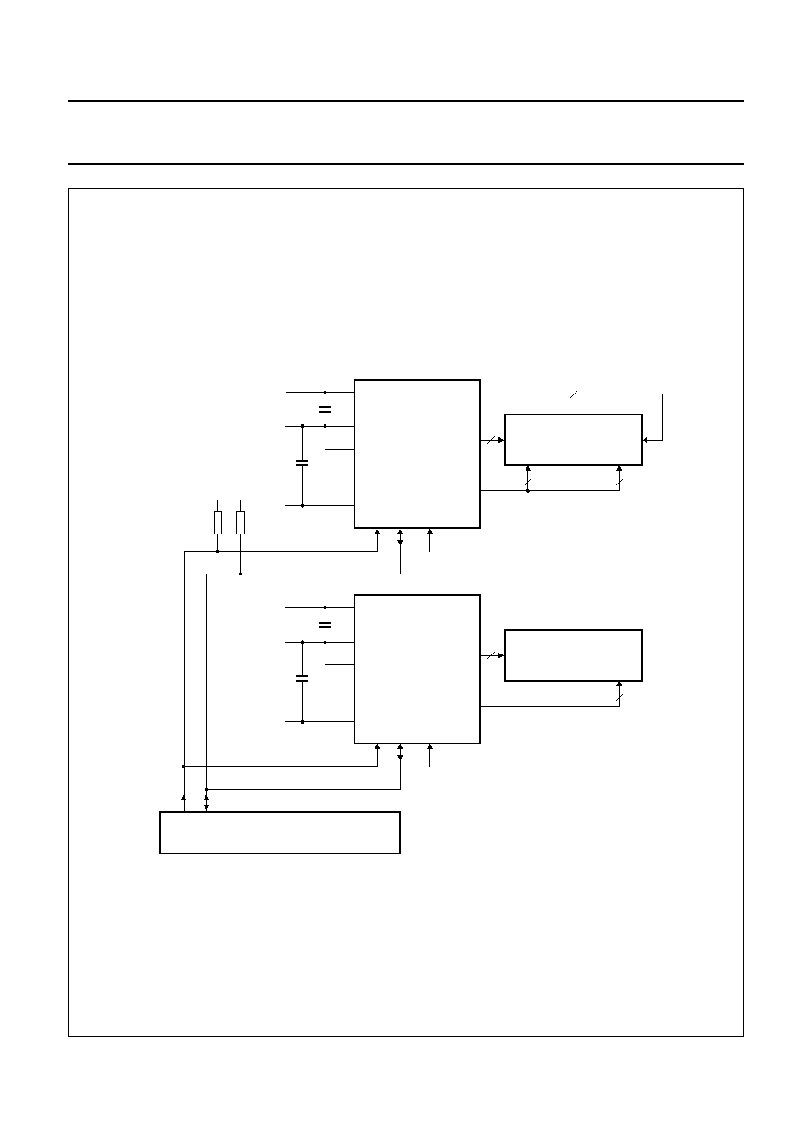
SA0: address input
The hardware subaddress line is used to program the
device subaddress for 2 different PCF2105s on the same
I
2
C-bus.
7.12
T1: test input
Pad T1 must be connected to V
SS
. Not user accessible.
8
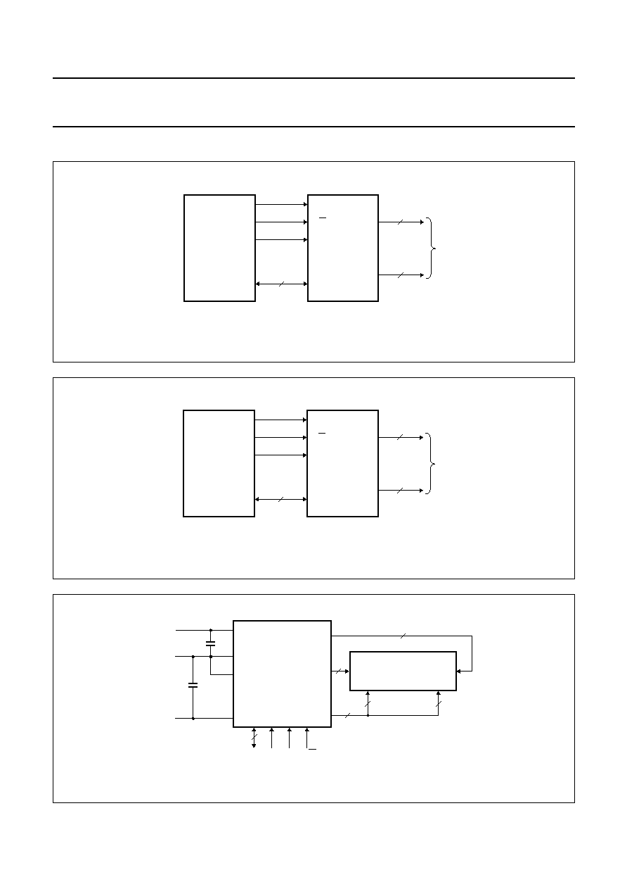
FUNCTIONAL DESCRIPTION
Figure 1 shows the block diagram for the PCF2105.
Details are explained in subsequent sections.
8.1
LCD bias voltage generator
The intermediate bias voltages for the LCD are generated
on-chip. This removes the need for an external resistive
bias chain and significantly reduces the system power
consumption. The optimum levels depend on the multiplex
(MUX) rate and are selected automatically when the
number of lines in the display is defined.
The optimum value of the LCD operating voltage V
OP
depends on the MUX rate, the LCD threshold voltage V
th
and the number of bias levels. The relationships, together
with the discrimination ratio (D) are given in Table 1.
Using a 5-level bias scheme for MUX rate 1 : 16 allows
V
OP
< 5 V for most LCDs. The effect on the display
contrast is negligible.
Table 1
Optimum values for V
OP
MUX
RATE
NUMBER
OF BIAS
LEVELS
1 : 16
5
3.67
1.277
1 : 32
6
5.19
1.196
v
OP
v
th
----------
D
V
on
V
off
---------
=
8.2
Oscillator
The on-chip oscillator provides the clock signal for the
display system. No external components are required.
Pad OSC must be connected to V
DD
.
8.3
External clock
If an external clock is to be used, it must be input at
pad OSC. The resulting display frame frequency is given
by
A clock signal must always be present, otherwise the LCD
may be frozen in a DC state.
8.4
Power-on reset
The Power-on reset block initializes the chip after
power-on or power failure.
8.5
Registers
The PCF2105 has two 8-bit registers, an Instruction
Register (IR) and a Data Register (DR). The Register
Select (RS) signal determines which register will be
accessed.
The IR stores instruction codes such as `clear display' and
`cursor shift', and address information for the DDRAM
and CGRAM. The system controller can write data to but
can not read data from the instruction register.
The DR temporarily stores data to be read from the
DDRAM and CGRAM. When reading, data from the
DDRAM or CGRAM (corresponding to the address in the
address counter) is written to the DR prior to being read by
the `read data' instruction.
8.6
Busy flag
The Busy Flag (BF) indicates the free or busy status of the
PCF2105. Bit BF = 1 indicates that the chip is busy and
further instructions will not be accepted. The BF is output
at pad DB7 when bit RS = 0 and bit R/W = 1. Instructions
should only be written after checking that BF = 0 or waiting
for the required number of clock cycles.
8.7
Address Counter (AC)
The AC assigns addresses to the DDRAM and CGRAM for
reading and writing and is set by the instructions `set
CGRAM address' and `set DDRAM address'. After a
read/write operation the AC is automatically incremented
or decremented by 1. The AC contents are output to the
bus (pads DB6 to DB0) when bit RS = 0 and bit R/W =1.
f
frame
f
osc
2304
-------------
=

1998 Jul 30
7
Philips Semiconductors
Product specification
LCD controller/driver
PCF2105
8.8
Display Data RAM (DDRAM)
The DDRAM stores up to 80 characters of display data,
represented by 8-bit character codes. DDRAM locations
not used for storing display data can be used as general
purpose RAM. The basic DDRAM-to-display mapping
scheme is shown in Fig.2. With no display shift, the
characters represented by the codes in the first
12 or 24 DDRAM locations, starting at address 00 in
line 1, are displayed. Subsequent lines display data
starting at addresses 20, 40, or 60 hexadecimal (hex).
Figures 3 and 4 show the DDRAM-to-display mapping
scheme when the display is shifted.
The address range for a 1-line display is 00 to 4F; for a
2-line display from 00 to 27 (line 1) and 40 to 67 (line 2);
for a 4-line display from 00 to 13, 20 to 33, 40 to 53 and
60 to 73 for lines 1, 2, 3 and 4 respectively. For 2 and
4-line displays the end address of one line and the start
address of the next line are not successive. When the
display is shifted each line wraps around independently of
the others (see Figs 3 and 4).
When data is written to the DDRAM, wrap-around occurs
from 4F to 00 in 1-line display and from 27 to 40 and
67 to 00 in 2-line display; from 13 to 20, 33 to 40, 53 to 60
and 73 to 00 in 4-line display.
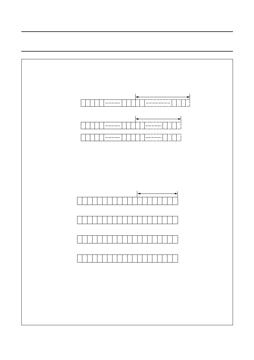
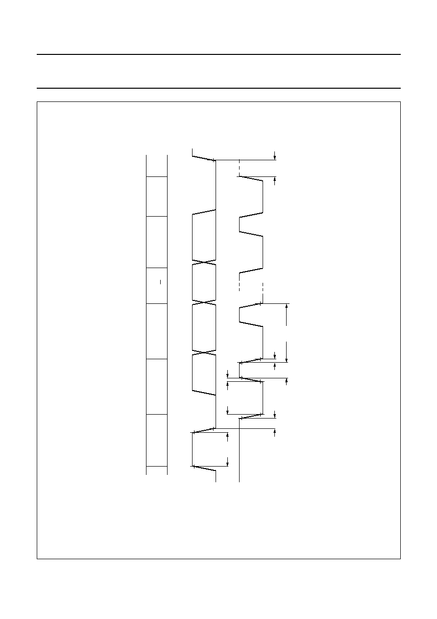
8.9
Character Generator ROM (CGROM)
The CGROM generates 240 character patterns in 5
×
8
dot format from 8-bit character codes. Figure 5 shows the
character set currently available.
8.10
Character Generator RAM (CGRAM)
Up to 16 user-defined characters may be stored in the
CGRAM. The CGROM and CGRAM use a common
address space, of which the first column is reserved for the
CGRAM (see Fig.5). Figure 6 shows the addressing
principle for the CGRAM.
8.11
Cursor control circuit
The cursor control circuit generates the cursor (underline
and/or character blink as shown in Fig.7) at the DDRAM
address contained in the address counter. When the
address counter contains the CGRAM address the cursor
will be inhibited.
8.12
Timing generator
The timing generator produces the various signals
required to drive the internal circuitry. Internal chip
operation is not disturbed by operations on the data buses.
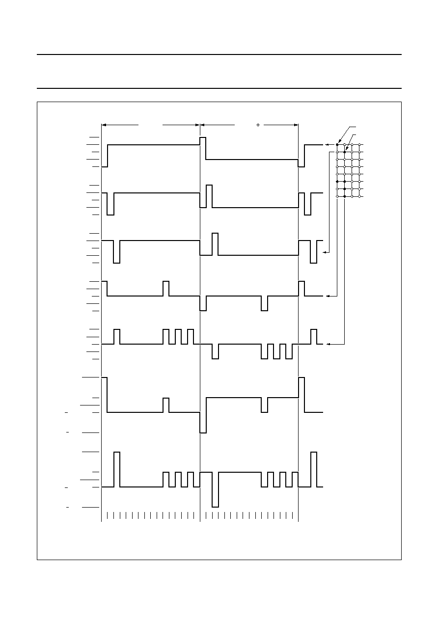
8.13
LCD row and column drivers
The PCF2105 contains 32 row drivers and 60 column
drivers. They connect the appropriate LCD bias voltages in
sequence to the display, in accordance with the data to be
displayed. The bias voltages and the timing are selected
automatically when the number of lines in the display is
selected. Figures 8 and 9 show typical waveforms.
In the 1-line display (MUX rate 1 : 16), the row outputs are
driven in pairs, for example R1/R17 and R2/R18.
This allows the output pairs to be connected in parallel,
thereby providing greater drive capability.
Unused outputs should be left unconnected.
1998 Jul 30
8
Philips Semiconductors
Product specification
LCD controller/driver
PCF2105
Fig.2 DDRAM-to-display mapping; no shift.
handbook, 4 columns
1
2
3
4
5
6
7
8
9 10 11 12
non-displayed DDRAM addresses
DDRAM
Address
(hex)
4 line display
00 01 02 03 04 05 06 07 08 09 0A 0B 0C 0D 0E 0F
10 11 12
13
20 21 22 23 24 25 26 27 28 29 2A 2B 2C 2D 2E 2F
30 31 32 33
40 41 42 43 44 45 46 47 48 49 4A 4B 4C 4D 4E 4F 50 51
52 53
60 61 62 63 64 65 66 67 68 69 6A 6B 6C 6D 6E 6F 70 71 72 73
line 1
line 2
line 3
line 4
MLA793
handbook, 4 columns
1
2
3
4
5
22 23 24
00 01 02 03 04
15 16 17 18 19
4C 4D 4E 4F
non-displayed DDRAM addresses
Display
Position
(decimal)
DDRAM
Address
(hex)
1-line display
64 65 66 67
40 41 42 43 44
55 56 57 58 59
00 01 02 03 04
15 16 17 18 19
24 25 26 27
non-displayed DDRAM address
DDRAM
(hex)
Address
2-line display
line 1
line 2
MLA792

1998 Jul 30
9
Philips Semiconductors
Product specification
LCD controller/driver
PCF2105
Fig.3 DDRAM-to-display mapping; right shift.
27 00 01 02 03
67 40 41 42 43
14 15 16
54 55 56
DDRAM
Address
(hex)
line 1
line 2
2-line display
1
2
3
4
5
22 23 24
4F 00 01 02 03
14 15 16
Display
Position
(decimal)
DDRAM
Address
(hex)
1-line display
MLA802
13
01 02 03 04 05 06 07 08 09 0A
20 21 22 23 24 25 26 27 28 29 2A
33
40 41 42 43 44 45 46 47 48 49 4A
53
60 61 62 63 64 65 66 67 68 69 6A
73
1
2
3
4
5
6
7
8 9 10 11 12
DDRAM
Address
(hex)
line 1
line 2
line 3
line 4
4-line display
00
MLA803
Fig.4 DDRAM-to-display mapping; left shift.
1
2
3
4
5
22 23 24
05
01 02 03 04
16 17 18
41 42 43 44 45
56 57 58
05
01 02 03 04
16 17 18
Display
Position
(decimal)
DDRAM
Address
(hex)
DDRAM
Address
(hex)
line 1
line 2
1-line display
2-line display
MLA815
01 02 03 04 05 06 07 08 09 0A 0B 0C
21 22 23 24 25 26 27 28 29 2A 2B 2C
41 42 43 44 45 46 47 48 49 4A 4B 4C
61 62 63 64 65 66 67 68 69 6A 6B 6C
1
2
3
4
5
6
7
8
9 10 11 12
DDRAM
Address
(hex)
line 1
line 2
line 3
line 4
4-line display
MLA816
1998 Jul 30
10
Philips Semiconductors
Product specification
LCD controller/driver
PCF2105
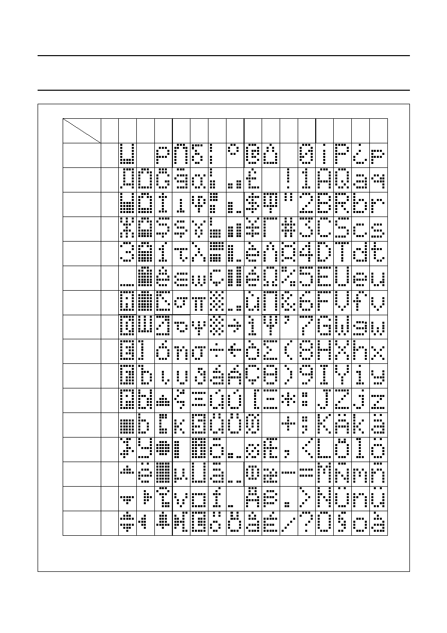
Fig.5 Character set `M' in CGROM.
handbook, full pagewidth
MGK847
0000
0001
0010
0011
0100
0101
0110
0111
1000
1001
1010
1011
1100
1101
1110
1111
upper
4 bits
lower
4 bits
xxxx 0000
xxxx 0001
xxxx 0010
xxxx 0011
xxxx 0100
xxxx 0101
xxxx 0110
xxxx 0111
xxxx 1000
xxxx 1001
xxxx 1010
xxxx 1011
xxxx 1100
xxxx 1101
xxxx 1110
xxxx 1111
16
15
14
13
12
11
10
9
8
7
6
5
4
3
2
CG
RAM 1

1998 Jul 30
11
Philips Semiconductors
Product specification
LCD controller/driver
PCF2105
Fig.6 Relationship between CGRAM addresses, data and display patterns.
Character code bits 0 to 3 correspond to CGRAM address bits 3 to 6.
CGRAM address bits 0 to 2 designate character pattern line position. The 8th line is the cursor position and display is performed by logical OR with the
cursor. Data in the 8th line will appear in the cursor position.
Character pattern column positions correspond to CGRAM data bits 0 to 4; bit 4 being at the left end, as shown in this figure.
CGRAM character patterns are selected when character code bits 4 to 7 are all logic 0. CGRAM data is logic 1 corresponds to selection for display.
Only bits 0 to 5 of the CGRAM address are set by the `set CGRAM address' instruction. Bit 6 can be set using the `set DDRAM address' instruction or
by using the auto-increment feature during CGRAM write. All bits 0 to 6 can be read using the `read busy flag and address' instruction.
handbook, full pagewidth
MGA800 - 1
7
6
5
4
3
2
1
0
6
5
4
3
2
1
0
4
3
2
1
0
higher
order
bits
lower
order
bits
lower
order
bits
higher
order
bits
lower
order
bits
higher
order
bits
0
0
0
0
0
0
0
0
0
0
0
0
0
0
0
0
0
0
1
0
0
0
0
1
0
0
0
0
0
1
1
0
1
0
0
0
0
0
1
0
1
0
0
0
1
1
0
0
0
0
1
1
1
0
0
0
0
0
0
0
0
0
0
0
0
0
1
0
0
0
0
1
0
0
0
0
0
0
1
1
1
0
0
1
0
1
0
0
0
0
1
1
0
0
0
0
0
1
1
1
0
0
0
0
0
0
0
1
0
0
0
0
0
0
0
1
0
0
0
1
0
0
0
0
0
0
1
0
0
0
0
0
1
1
1
1
0
0
0
0
1
1
1
1
0
0
0
0
1
1
1
1
0
0
0
0
1
1
1
1
0
1
0
0
0
0
0
1
0
0
1
0
1
1
1
0
1
1
1
1
1
1
1
1
1
1
1
1
1
1
1
1
1
1
1
character codes
(DDRAM data)
CGRAM
address
character patterns
(CGRAM data)
character
pattern
example 1
cursor
position
character
pattern
example 2
1998 Jul 30
12
Philips Semiconductors
Product specification
LCD controller/driver
PCF2105
Fig.7 Cursor and blink display examples.
MGA801
cursor
5 x 7 dot character font
alternating display
cursor display example
blink display example
1998 Jul 30
13
Philips Semiconductors
Product specification
LCD controller/driver
PCF2105
Fig.8 Typical LCD waveforms; 1-line display.
handbook, full pagewidth
MGA802 - 1
VDD
V2
V
V
5
LCD
ROW 1
COL 1
state 1 (ON)
state 2 (ON)
0.25 VOP
0 V
state 1
1-line display
(1:16)
frame n 1
frame n
ROW 9
ROW 2
COL 2
state 2
1 2 3
16 1 2 3
16
3
4
V /V
VDD
V2
V
V
5
LCD
3
4
V /V
VDD
V2
V
V
5
LCD
3
4
V /V
VDD
V2
V
V
5
LCD
3
4
V /V
VDD
V2
V
V
5
LCD
3
4
V /V
0.25 VOP
0.25 VOP
0 V
0.25 VOP
VOP
VOP
VOP
VOP

1998 Jul 30
14
Philips Semiconductors
Product specification
LCD controller/driver
PCF2105
Fig.9 Typical LCD waveforms; 2-line display.
handbook, full pagewidth
MGA803 - 1
VDD
V 2
V
V
V
V
3
4
5
LCD
ROW 1
VDD
V 2
V
V
V
V
3
4
5
LCD
VDD
V 2
V
V
V
V
3
4
5
LCD
COL 1
VDD
V 2
V
V
V
V
3
4
5
LCD
state 1 (ON)
state 2 (ON)
0.15 VOP
0 V
VOP
VOP
VOP
state 1
2-line display
(1:32)
frame n 1
frame n
ROW 9
ROW 2
COL 2
VDD
V 2
V
V
V
V
3
4
5
LCD
0.15 VOP
0.15 VOP
0 V
0.15 VOP
VOP
state 2
1 2 3
32 1 2 3
32

1998 Jul 30
15
Philips Semiconductors
Product specification
LCD controller/driver
PCF2105
8.14
Programming of the MUX rate 1 : 16
With the MUX rate 1 : 16 the PCF2105 can be used in the
following ways:
·
To drive a 1-line display of 24 characters
·
To drive a 2-line display of 12 characters, resulting in
better contrast. The internal data flow of the chip is
optimized for this purpose.
To program the MUX rate 1 : 16, bits M and N of the
`function set' instruction must be set to logic 0
(see Table 3). Figures 10, 11 and 12 show the DDRAM
addresses of the display characters. The second row of
each figure corresponds to either the right half of a 1-line
display or to the second line of a 2-line display. Wrap
around of data during display shift or when writing data is
non-standard.
Fig.10 DDRAM-to-display mapping; no shift.
handbook, full pagewidth
00
01
02
03
04
05
06
07
08
09
0A
0B
1
2
3
4
5
6
7
8
9
10
11
12
MLB899
display position
DDRAM address
0C
0D
0E
0F
10
11
12
13
14
15
16
17
13
14
15
16
17
18
19
20
21
22
23
24
display position
DDRAM address
Fig.11 DDRAM-to-display mapping; right shift.
handbook, full pagewidth
4F
00
01
02
03
04
05
06
07
08
09
0A
1
2
3
4
5
6
7
8
9
10
11
12
MLB900
display position
DDRAM address
0B
0C
0D
0E
0F
10
11
12
13
14
15
16
13
14
15
16
17
18
19
20
21
22
23
24
display position
DDRAM address
Fig.12 DDRAM-to-display mapping; left shift.
handbook, full pagewidth
01
02
03
04
05
06
07
08
09
0A
0B
0C
1
2
3
4
5
6
7
8
9
10
11
12
MLB901
display position
DDRAM address
0D
0E
0F
10
11
12
13
14
15
16
17
18
13
14
15
16
17
18
19
20
21
22
23
24
display position
DDRAM address

1998 Jul 30
16
Philips Semiconductors
Product specification
LCD controller/driver
PCF2105
8.15
Programming of the MUX rate 1 : 32
With the MUX rate 1 : 32 the PCF2105 can be used in the
following ways:
·
To drive a 2-line display of 24 characters, use instruction
`function set' to set bit M to logic 0 and bit N to logic 1
·
To drive a 4-line display of 12 characters, use instruction
`function set' to set both bits M and N to logic 1.
8.16
Reset function
The PCF2105 automatically initializes (resets) when
power is turned on. The state after reset is given in Table 2
(see Tables 3 and 4 for the description of the bits).
Table 2
State after reset
9
INSTRUCTIONS
Only two PCF2105 registers, the Instruction Register (IR)
and the Data Register (DR) can be directly controlled by
the microcontroller. Before internal operation, control
information is stored temporarily in these registers to allow
interface to various types of microcontrollers which
operate at different speeds or to allow interfacing to
peripheral control ICs. The PCF2105 operation is
controlled by the instructions shown in Table 3 together
with their execution time. Details are explained in
subsequent sections.
STEP
DESCRIPTION
1
clear display
2
function set:
bit DL = 1: 8-bit interface
bits M and N = 0: 1-line display
bit G = 0: not used
3
display control:
bit D = 0: display off
bit C = 0: cursor off
bit B = 0: blink off
4
entry mode set:
bit I/D = 1: +1(increment)
bit G = 0: not used
5
default address pointer to DDRAM; the busy
flag indicates the busy state (BF = 1) until
initialization ends; the busy state lasts 2 ms;
the chip may also be initialized by software;
see Tables 10 and 11.
6
I
2
C-bus interface reset
Instructions are of 4 categories, those that:
1. Designate PCF2105 functions such as display format,
data length, etc.
2. Set internal RAM addresses
3. Perform data transfer with internal RAM
4. Others.
In normal use, category 3 instructions are used most
frequently. However, automatic incrementing by 1 (or
decrementing by 1) of internal RAM addresses after each
data write lessens the microcontroller program load.
The display shift in particular can be performed
concurrently with display data write, thus enabling the
designer to develop systems in minimum time with
maximum programming efficiency.
During internal operation, no instruction other than the
`read busy flag and address' will be executed.
Because the busy flag is set to logic 1 while an instruction
is being executed, it is advisable to ensure that the flag is
set to logic 0 before sending the next instruction or wait for
the maximum instruction execution time, as given in
Table 3. An instruction sent while the busy flag is HIGH will
not be executed.
9.1
Clear display
`Clear display' writes space code 20 (hexadecimal) into all
DDRAM addresses (the character pattern for character
code 20 must be a blank pattern), sets the DDRAM
address counter to logic 0 and returns the display to its
original position if it was shifted. Consequently, the display
disappears and the cursor or blink position goes to the left
edge of the display (the first line if 2 or 4 lines are
displayed) and sets bit I/D of `entry mode set' to logic 1
(increment mode). Bit S of `entry mode set' does not
change.
The instruction `clear display' requires extra execution
time. This may be allowed for checking the Busy Flag (BF)
or by waiting until 2 ms has elapsed. The latter must be
applied where no read-back options are available, as in
some Chip-On-Glass (COG) applications.
9.2
Return home
`Return home' sets the DDRAM address counter to logic 0
and returns the display to its original position if it was
shifted. DDRAM contents do not change. The cursor or
blink position goes to the left of the display (the first line if
2 or 4 lines are displayed). Bits I/D and S of `entry mode
set' do not change.

1998
Jul
30
17
Philips Semiconductors
Product specification
LCD controller/driver
PCF2105
This text is here in white to force landscape pages to be rotated correctly when browsing through the pdf in the Acrobat reader.This text is here in
_
white to force landscape pages to be rotated correctly when browsing through the pdf in the Acrobat reader.This text is here inThis text is here in
white to force landscape pages to be rotated correctly when browsing through the pdf in the Acrobat reader. white to force landscape pages to be ...
Table 3
Instructions (note 1)
Notes
1. In the I
2
C-bus mode the DL bit is don't care. 8-bit mode is assumed. In the I
2
C-bus mode a control byte is required when bit RS or R/W is changed;
control byte: Co, RS, R/W, 0, 0, 0, 0, 0; command byte: DB7 to DB0.
2. Example: f
osc
= 150 kHz,
; 3 cycles = 20
µ
s; 165 cycles = 1.1 ms.
INSTRUCTION
RS
R/W
DB7
DB6
DB5
DB4
DB3
DB2
DB1
DB0
DESCRIPTION
REQUIRED
CLOCK
CYCLES
(2)
NOP
0
0
0
0
0
0
0
0
0
0
no operation
0
Clear display
0
0
0
0
0
0
0
0
0
1
clears entire display and sets DDRAM
address 00 in Address Counter (AC)
165
Return home
0
0
0
0
0
0
0
0
1
0
sets DDRAM address 00 in the AC;
also returns shifted display to original
position; DDRAM contents remain
unchanged
3
Entry mode set
0
0
0
0
0
0
0
1
I/D
S
sets cursor move direction and specifies
shift of display; these operations are
performed during data write and read
3
Display control
0
0
0
0
0
0
1
D
C
B
sets entire display on/off (D), cursor
on/off (C) and blink of cursor position
character (B)
3
Cursor/display shift
0
0
0
0
0
1
S/C
R/L
0
0
moves cursor and shifts display without
changing DDRAM contents
3
Function set
0
0
0
0
1
DL
N
M
G
0
sets interface data length (DL), number
of display lines (N, M) and voltage
generator control (G); bit G is not used
3
Set CGRAM
address
0
0
0
1
A
CG
sets CGRAM address
3
Set DDRAM
address
0
0
1
A
DD
sets DDRAM address
3
Read busy flag and
address
0
1
BF
A
C
reads BF indicating internal operation is
being performed and reads AC contents
0
Read data
1
1
read data
reads data from CGRAM or DDRAM
3
Write data
1
0
write data
writes data to CGRAM or DDRAM
3
T
cy
1
f
osc
--------
6.67
µ
s
=
=

1998 Jul 30
18
Philips Semiconductors
Product specification
LCD controller/driver
PCF2105
Table 4
Command bit identities, used in Table 3
BIT
LOGIC 0
LOGIC 1
I/D
decrement
increment
S
display freeze
display shift
D
display off
display on
C
cursor off
cursor on
B
character at cursor position does not blink
character at cursor position blinks
S/C
cursor move
display shift
R/L
left shift
right shift
DL
4 bits
8 bits
N (M = 0)
2 lines
×
12 characters; MUX rate 1 : 16
2 lines
×
24 characters; MUX rate 1 : 32
N (M = 1)
reserved
4 lines
×
12 characters; MUX rate 1 : 32
BF
end of internal operation
internal operation in progress
Co
last control byte, only data bytes to follow
next two bytes are a data byte and another control byte
9.3
Entry mode set
9.3.1
I/D
When bit I/D = 1 (0), the DDRAM or CGRAM address
increments (decrements) by 1 when data is written to or
read from the DDRAM or CGRAM. The cursor or blink
position moves to the right when incremented and to the
left when decremented. The cursor and blink are inhibited
when the CGRAM is accessed.
9.3.2
S
When bit S = 1, the entire display shifts either to the right
(bit I/D = 0) or to the left (I/D = 1) during a DDRAM write.
Consequently, it looks as if the cursor stands still and the
display moves. The display does not shift when reading
from the DDRAM, or when writing to or reading from the
CGRAM. When S = 0 the display does not shift.
9.4
Display control
9.4.1
D
The display is on when bit D = 1 and off when D = 0.
Display data in the DDRAM is not affected and can be
displayed immediately by setting D to logic 1.
9.4.2
C
The cursor is displayed when bit C = 1 and inhibited when
C = 0. Even if the cursor disappears, the display functions,
I/D, etc. remain in operation during display data write.
The cursor is displayed using 5 dots in the 8th line
(see Fig.7).
9.4.3
B
The character indicated by the cursor blinks when
bit B = 1. The blink is displayed by switching between
display characters and all dots on with a period of
1 second when f
osc
= 150 kHz (see Fig.7).
At other clock frequencies the blink period is equal to
The cursor and the blink can be set to display
simultaneously.
9.5
Cursor/display shift
`Cursor/display shift' moves the cursor position or the
display to the right or left without writing or reading display
data. This function is used to correct a character or move
the cursor through the display. In the 2 or 4-line display,
the cursor moves to the next line when it passes the last
position of the line (40 or 20 decimal). When the displayed
data is shifted repeatedly all lines shift at the same time;
displayed characters do not shift into the next line.
The Address Counter (AC) content does not change if the
only action performed is shift display, but increments or
decrements with the cursor shift.
150 kHz
f
osc
----------------------
1998 Jul 30
19
Philips Semiconductors
Product specification
LCD controller/driver
PCF2105
9.6
Function set
9.6.1
DL (
PARALLEL MODE ONLY
)
Bit DL sets the interface data length. Data is sent or
received in bytes (DB7 to DB0) when DL = 1 or in two
nibbles (DB7 to DB4) when DL = 0. When 4-bit length is
selected, data is transmitted in two cycles using the
parallel bus. In a 4-bit application DB3 to DB0 are left open
(internal pull-ups).
DL can not be set to logic 0 from the I
2
C-bus interface.
If DL has been set to logic 0 via the parallel bus,
programming via the I
2
C-bus interface is complicated.
9.6.2
N
AND
M
Bits N and M set the number of display lines.
9.7
Set CGRAM address
`Set CGRAM address' sets bits 0 to 5 of the CGRAM
address (A
CG
in Table 3) into the AC (binary A[5] to A[0]).
Data can then be written to or read from the CGRAM.
Only bits 0 to 5 of the CGRAM address are set by the `set
CGRAM address' instruction. Bit 6 can be set using the
`set DDRAM address' instruction or by using the
auto-increment feature during CGRAM write. All bits 0 to 6
can be read using the `read busy flag and address'
instruction.
9.8
Set DDRAM address
`Set DDRAM address' sets the DDRAM address (A
DD
in
Table 3) into the AC (binary A[6] to A[0]). Data can then be
written to or read from the DDRAM.
Table 5
Hexadecimal address ranges
ADDRESS
FUNCTION
00 to 4F
1 line of 24 characters
00 to 0B and 0C to 4F
2 lines of 12 characters
00 to 27 and 40 to 67
2 lines of 24 characters
00 to 13, 20 to 33, 40 to 53
and 60 to 73
4 lines of 12 characters
9.9
Read busy flag and address
`Read busy flag and address' reads the Busy Fag (BF).
When bit BF = 1 it indicates that an internal operation is in
progress. The next instruction will not be executed until
BF = 0, so BF should be checked before sending another
instruction.
At the same time, the value of the AC expressed in binary
A[6] to A[0] is read out. The address counter is used by
both CGRAM and DDRAM and its value is determined by
the previous instruction.
9.10
Write data to CGRAM or DDRAM
`Write data' writes binary 8-bit data (D[7] to D[0]) to the
CGRAM or the DDRAM.
Whether the CGRAM or DDRAM is to be written to is
determined by the previous specification of CGRAM or
DDRAM address setting. After writing, the address
automatically increments or decrements by 1, in
accordance with the `entry mode set`.
Only bits D[4] to D[0] of CGRAM data are valid,
bits D[7] to D[5] are `don't care'.
9.11
Read data from CGRAM or DDRAM
`Read data' reads binary 8-bit data D[7] to D[0] from the
CGRAM or DDRAM.
The most recent `set address' instruction determines
whether the CGRAM or DDRAM is to be read.
The `read data' instruction gates the content of the
Data Register (DR) to the bus while pad E = HIGH. After E
goes LOW again, internal operation increments
(or decrements) the AC and stores RAM data
corresponding to the new AC into the DR.
Remark: the only three instructions that update the DR are:
·
`Set CGRAM address'
·
`Set DDRAM address'
·
`Read data' from CGRAM or DDRAM.
Other instructions (e.g. `write data', `cursor/display shift',
`clear display', `return home') will not change the data
register content.
1998 Jul 30
20
Philips Semiconductors
Product specification
LCD controller/driver
PCF2105
10 INTERFACE TO MICROCONTROLLER
(PARALLEL INTERFACE)
The PCF2105 can send data in either two 4-bit modes or
one 8-bit mode and can thus interface to 4 or 8-bit
microcontrollers.
In the 8-bit mode data is transferred as 8-bit bytes using
the 8 data lines DB7 to DB0. The control lines E, RS,
and R/W are required.
In the 4-bit mode data is transferred in two cycles of 4-bits
each. The higher order bits (corresponding to DB7 to DB4
in 8-bit mode) are sent in the first cycle and the lower order
bits (DB3 to DB0 in 8-bit mode) in the second cycle. Data
transfer is complete after two 4-bit data transfers. It should
be noted that two cycles are also required for the busy flag
check. The 4-bit mode is selected by instruction.
See Figs 13, 14 and 15 for examples of bus protocol.
In the 4-bit mode, the pads DB3 to DB0 must be left
open-circuit. They are pulled up to V
DD
internally.
Fig.13 4-bit transfer example.
MGA804
RS
E
DB7
R/W
DB6
DB5
DB4
instruction
write
busy flag and
address counter read
data register
read
IR7
IR3
BF
AC3
DR7
DR3
IR6
IR2
AC6
AC2
DR6
DR2
IR5
IR1
AC5
AC1
DR5
DR1
IR4
IR0
AC4
AC0
DR4
DR0

1998 Jul 30
21
Philips Semiconductors
Product specification
LCD controller/driver
PCF2105
Fig.14 An example of 4-bit data transfer timing sequence.
IR7 and IR3: instruction 7th bit and 3rd bit.
AC3: address counter 3rd bit.
MGA805
RS
E
internal
DB7
R/W
internal operation
IR7
IR3
AC3
D7
D3
not
busy
AC3
busy
instruction
write
busy flag
check
busy flag
check
instruction
write
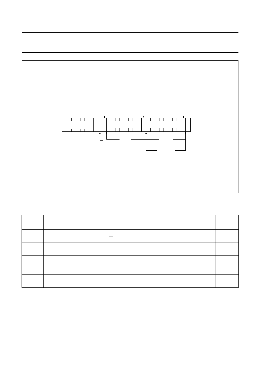
Fig.15 Example of busy flag check timing sequence.
MGA806
instruction
write
busy flag
check
busy flag
check
busy flag
check
instruction
write
internal operation
RS
E
internal
DB7
R/W
data
busy
busy
not
busy
data

1998 Jul 30
22
Philips Semiconductors
Product specification
LCD controller/driver
PCF2105
11 INTERFACE TO MICROCONTROLLER (I
2
C-BUS
INTERFACE)
11.1
Characteristics of the I
2
C-bus
The I
2
C-bus is for bidirectional, 2-line communication
between different ICs or modules. The 2 lines are a serial
data line (SDA) and a serial clock line (SCL). Both lines
must be connected to a positive supply via a pull-up
resistor. Data transfer may be initiated only when the bus
is not busy.
11.2
Bit transfer
One data bit is transferred during each clock pulse.
The data on the SDA line must remain stable during the
HIGH-level period of the clock pulse as changes in the
data line at this time will be interpreted as a control signal
(see Fig.16).
11.3
START and STOP conditions
Both data and clock lines remain HIGH when the bus is not
busy. A HIGH-to-LOW transition of the data line, while the
clock is HIGH is defined as the START condition (S).
A LOW-to-HIGH transition of the data line while the clock
is HIGH is defined as the STOP condition (P) (see Fig.17).
11.4
System configuration
A device generating a message is a transmitter, a device
receiving a message is the receiver. The device that
controls the message is the master and the devices which
are controlled by the master are the slaves (see Fig.18).
11.5
Acknowledge
The number of data bytes transferred between the START
and STOP conditions from transmitter to receiver is
unlimited. Each byte of 8 bits is followed by an
acknowledge bit. The acknowledge bit is a HIGH signal put
on the bus by the transmitter during which time the master
generates an extra acknowledge related clock pulse.
A slave receiver which is addressed must generate an
acknowledge after the reception of each byte. Also a
master receiver must generate an acknowledge after the
reception of each byte that has been clocked out of the
slave transmitter. The device that acknowledges must
pull-down the SDA line during the acknowledge clock
pulse, so that the SDA line is stable LOW during the HIGH
period of the acknowledge related clock pulse (set-up and
hold times must be taken into consideration). A master
receiver must signal an end of data to the transmitter by
not generating an acknowledge on the last byte that has
been clocked out of the slave. In this event the transmitter
must leave the data line HIGH to enable the master to
generate a STOP condition (see Fig.19).
11.6
I
2
C-bus protocol
Before any data is transmitted on the I
2
C-bus, the device
which should respond is addressed first. The addressing is
always carried out with the first byte transmitted after the
start procedure. The I
2
C-bus configuration for the different
PCF2105 read and write cycles is illustrated in
Figs 20, 21 and 22.
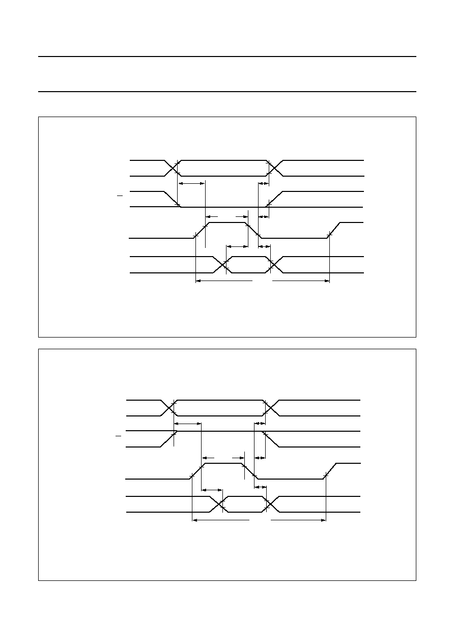
Fig.16 Bit transfer.
handbook, full pagewidth
MBC621
data line
stable;
data valid
change
of data
allowed
SDA
SCL
1998 Jul 30
23
Philips Semiconductors
Product specification
LCD controller/driver
PCF2105
Fig.17 Definition of START and STOP conditions.
handbook, full pagewidth
MBC622
SDA
SCL
P
STOP condition
SDA
SCL
S
START condition
Fig.18 System configuration.
MGA807
SDA
SCL
MASTER
TRANSMITTER/
RECEIVER
MASTER
TRANSMITTER
SLAVE
TRANSMITTER/
RECEIVER
SLAVE
RECEIVER
MASTER
TRANSMITTER/
RECEIVER
Fig.19 Acknowledgement on the I
2
C-bus.
handbook, full pagewidth
MBC602
S
START
condition
9
8
2
1
clock pulse for
acknowledgement
not acknowledge
acknowledge
DATA OUTPUT
BY TRANSMITTER
DATA OUTPUT
BY RECEIVER
SCL FROM
MASTER

1998
Jul
30
24
Philips Semiconductors
Product specification
LCD controller/driver
PCF2105
This text is here in white to force landscape pages to be rotated correctly when browsing through the pdf in the Acrobat reader.This text is here in
_
white to force landscape pages to be rotated correctly when browsing through the pdf in the Acrobat reader.This text is here inThis text is here in
white to force landscape pages to be rotated correctly when browsing through the pdf in the Acrobat reader. white to force landscape pages to be ...
handbook, full pagewidth
S
A
0
S
0 1 1 1 0 1
0 A
slave address
CONTROL BYTE
A
DATA
A
DATA
A
R/W
acknowledgement
from PCF2105
CONTROL BYTE
A
MGK848
P
update
data pointer
1 byte
S
A
0
0 1 1 1 0 1
0
PCF2105
slave address
R/W
1
Co
0
Co
2n
0 bytes
n
0 bytes
Fig.20 Master transmits to slave receiver; write mode.
1998
Jul
30
25
Philips Semiconductors
Product specification
LCD controller/driver
PCF2105
This text is here in white to force landscape pages to be rotated correctly when browsing through the pdf in the Acrobat reader.This text is here in
_
white to force landscape pages to be rotated correctly when browsing through the pdf in the Acrobat reader.This text is here inThis text is here in
white to force landscape pages to be rotated correctly when browsing through the pdf in the Acrobat reader. white to force landscape pages to be ...
handbook, full pagewidth
S
A
0
S
0 1 1 1 0 1
0 A
slave address
CONTROL BYTE
A
1
Co
DATA
A
1 1
CONTROL
A
R/W
0
Co
2 bytes
DATA
A
acknowledgement
from PCF2105
MGK849
S
A
0
S
1 A
DATA
A
1
P
SLAVE
ADDRESS
DATA
acknowledgement
from PCF2105
no acknowledgement
from master
R/W
n bytes
last byte
update
data pointer
(1)
2n
0 bytes
Fig.21 Master reads after setting word address; write word address, set RS and R/W; read data.
(1) Last data byte is a dummy byte (may be omitted).
1998 Jul 30
26
Philips Semiconductors
Product specification
LCD controller/driver
PCF2105
12 LIMITING VALUES
In accordance with the Absolute Maximum Rating System (IEC 134).
13 HANDLING
Inputs and outputs are protected against electrostatic discharge in normal handling. However, to be totally safe, it is
desirable to take normal precautions appropriate to handling MOS devices (see
"Handling MOS Devices" ).
SYMBOL
PARAMETER
MIN.
MAX.
UNIT
V
DD
logic supply voltage
-
0.5
+8.0
V
V
LCD
LCD supply voltage
V
DD
-
11
V
DD
V
V
I(n)
input voltage on pads OSC, RS, R/W, E and DB0 to DB7
V
SS
-
0.5
V
DD
+ 0.5
V
V
O(n)
output voltage on pads R1 to R32, C1 to C60 and V
LCD
V
LCD
-
0.5
V
DD
+ 0.5
V
I
I(n)
DC input current on every pad
-
10
+10
mA
I
O(n)
DC output current on every pad
-
10
+10
mA
I
n
current on V
DD
, V
SS
and V
LCD
-
50
+50
mA
P
tot
total power dissipation
-
400
mW
P/out
power dissipation per output
-
100
mW
T
stg
storage temperature
-
65
+150
°
C
Fig.22 Master reads slave immediately after first byte; read mode (RS previously defined).
handbook, full pagewidth
MGK850
S
A
0
S
1 A
DATA
A
1
P
SLAVE
ADDRESS
DATA
acknowledgement
from PCF2105
no acknowledgement
from master
R/W
n bytes
last byte
update
data pointer
acknowledgement
from master

1998 Jul 30
27
Philips Semiconductors
Product specification
LCD controller/driver
PCF2105
14 DC CHARACTERISTICS
V
DD
= 2.5 to 6 V; V
SS
= 0 V; V
LCD
= V
DD
-
3.5 to V
DD
-
9 V; T
amb
=
-
40 to +85
°
C; unless otherwise specified.
SYMBOL
PARAMETER
CONDITIONS
MIN.
TYP.
MAX.
UNIT
Supplies
V
DD
logic supply voltage
2.5
-
6.0
V
V
LCD
LCD supply voltage
V
DD
-
9
-
V
DD
-
3.5 V
I
DD(ext)
external supply current
note 1
-
200
500
µ
A
V
DD
= 5 V; V
OP
= 9 V;
f
osc
= 150 kHz;
T
amb
= 25
°
C
-
200
300
µ
A
V
DD
= 3 V; V
OP
= 5 V;
f
osc
= 150 kHz;
T
amb
= 25
°
C
-
150
200
µ
A
I
I(LCD)
input current on V
LCD
note 1
-
50
100
µ
A
V
POR
Power-on reset voltage level
note 2
-
1.3
1.8
V
Logic
V
IL
LOW-level input voltage on pads E,
RS, R/W, DB7 to DB0 and SA0
V
SS
-
0.3V
DD
V
V
IH
HIGH-level input voltage on pads E,
RS, R/W, DB7 to DB0 and SA0
0.7V
DD
-
V
DD
V
V
IL(OSC)
LOW-level input voltage on pad OSC
V
SS
-
V
DD
-
1.5 V
V
IH(OSC)
HIGH-level input voltage on pad OSC
V
DD
-
0.1
-
V
DD
V
I
pu
pull-up current on pads DB7 to DB0,
RS and R/W
pads set to logic 0 (V
SS
)
0.04
0.15
1.00
µ
A
I
OL(DB)
LOW-level output current on
pads DB7 to DB0
V
OL
= 0.4 V; V
DD
= 5 V
1.6
-
-
mA
I
OH(DB)
HIGH-level output current on
pads DB7 to DB0
V
OH
= 4 V; V
DD
= 5 V
-
1.0
-
-
mA
I
L
leakage current on pads DB7 to DB0,
OSC, E, RS, R/W and SA0
pads set to logic 0 (V
SS
)
or logic 1 (V
DD
)
-
1
-
+1
µ
A
I
2
C-bus
SDA and SCL
V
IL
LOW-level input voltage
note 3
V
SS
-
0.3V
DD
V
V
IH
HIGH-level input voltage
note 3
0.7V
DD
-
V
DD
V
I
L
leakage current
pads set to logic 0 (V
SS
)
or logic 1 (V
DD
)
-
1
-
+1
µ
A
C
i
input capacitance
note 4
-
-
7
pF
I
OL(SDA)
LOW-level output current on SDA
V
OL
= 0.4 V; V
DD
= 5 V
3
-
-
mA
1998 Jul 30
28
Philips Semiconductors
Product specification
LCD controller/driver
PCF2105
Notes
1. LCD outputs are open-circuit; inputs at V
DD
or V
SS
; bus inactive; internal or external clock with duty factor 50%.
2. Resets all logic when V
DD
< V
POR
.
3. When the voltages are above V
DD
or below V
SS
, an input current may flow; this current must not exceed
±
0.5 mA.
4. Tested on sample basis.
5. Resistance of output terminals (R32 to R1 and C60 to C1) with load current I
L
= 150
µ
A; V
OP
= V
DD
-
V
LCD
= 9 V;
outputs measured one at a time.
6. LCD outputs open-circuit.
15 AC CHARACTERISTICS
V
DD
= 2.5 to 6.0 V; V
SS
= 0 V; V
LCD
= V
DD
-
3.5 V to V
DD
-
9 V; T
amb
=
-
40 to +85
°
C; unless otherwise specified.
LCD outputs
R
o(ROW)
row output resistance on
pads R32 to R1
note 5
-
1.5
3
k
R
o(COL)
column output resistance on
pads C60 to C1
note 5
-
3
6
k
V
bias(tol)
bias voltage tolerance on
pads R32 to R1 and C60 to C1
note 6
-
±
20
±
130
mV
SYMBOL
PARAMETER
CONDITIONS
MIN.
TYP.
MAX.
UNIT
f
fr(LCD)
LCD frame frequency (internal clock)
note 1
40
65
100
Hz
f
osc
oscillator frequency (external clock)
90
150
225
kHz
Bus timing characteristics: Parallel Interface; notes 1 and 2
W
RITE OPERATION
(
WRITING DATA FROM MICROCONTROLLER TO
PCF2105); see Fig.23
T
cy(en)
enable cycle time
500
-
-
ns
t
W(en)
enable pulse width
220
-
-
ns
t
su(A)
address set-up time
50
-
-
ns
t
h(A)
address hold time
25
-
-
ns
t
su(D)
data set-up time
60
-
-
ns
t
h(D)
data hold time
25
-
-
ns
R
EAD OPERATION
(
READING DATA FROM
PCF2105
TO MICROCONTROLLER
); see Fig.24
T
cy(en)
enable cycle time
500
-
-
ns
t
W(en)
enable pulse width
220
-
-
ns
t
su(A)
address set-up time
50
-
-
ns
t
h(A)
address hold time
25
-
-
ns
t
d(D)
data delay time
-
-
150
ns
t
h(D)
data hold time
20
-
100
ns
SYMBOL
PARAMETER
CONDITIONS
MIN.
TYP.
MAX.
UNIT

1998 Jul 30
29
Philips Semiconductors
Product specification
LCD controller/driver
PCF2105
Notes
1. V
DD
= 5.0 V.
2. All timing values are valid within the operating supply voltage and ambient temperature range and are referenced to
V
IL
and V
IH
with an input voltage swing of V
SS
to V
DD
.
3. C
L
= total capacitance of one bus line in pF and R = 100
.
4. A fast mode I
2
C-bus device can be used in a standard-mode I
2
C-bus system, but the requirement t
SU;DAT
250 ns
must then be met. This will automatically be the case if the device does not stretch the LOW period of the SCL signal.
If such a device does stretch the LOW period of the SCL signal, it must output the next data bit to the SDA line
t
r(max)
+ t
SU;DAT
= 1000 + 250 = 1250 ns (according to the standard-mode I
2
C-bus specification) before the SCL line
is released.
5. A device must internally provide a hold time of at least 300 ns for the SDA signal (referred to the V
IH(min)
of the SCL
signal) in order to bridge the undefined region of the falling edge of SCL.
6. The maximum t
HD;DAT
has only to be met if the device does not stretch t
LOW
of the SCL signal.
Timing characteristics: I
2
C-bus interface; note 2; see Fig.25
f
SCL
SCL clock frequency
-
-
400
kHz
t
SW
tolerable spike width on bus
-
-
50
ns
t
BUF
bus free time
1.3
-
-
µ
s
t
SU;STA
set-up time for a repeated START
condition
0.6
-
-
µ
s
t
HD;STA
START condition hold time
0.6
-
-
µ
s
t
LOW
SCL LOW time
1.3
-
-
µ
s
t
HIGH
SCL HIGH time
0.6
-
-
µ
s
t
r
SCL and SDA rise time
note 3
-
20 + RC
L
300
ns
t
f
SCL and SDA fall time
note 3
-
20 + RC
L
300
ns
t
SU;DAT
data set-up time
note 4
100
-
-
ns
t
HD;DAT
data hold time
notes 5 and 6
0
-
0.9
µ
s
t
SU;STO
set-up time for STOP condition
0.6
-
-
µ
s
C
L
load capacitance for each bus line
-
-
400
pF
SYMBOL
PARAMETER
CONDITIONS
MIN.
TYP.
MAX.
UNIT
1998 Jul 30
30
Philips Semiconductors
Product specification
LCD controller/driver
PCF2105
16 TIMING DIAGRAMS
Fig.23 Parallel bus write operation sequence; writing data from microcontroller to PCF2105.
handbook, full pagewidth
RS
E
DB0 to DB7
VIH
VIL
VIH
VIL
VIH
VIL
VIH
VIL
VIH
VIL
VIL
VIL
VIL
VIH
VIL
Tcy(en)
tW(en)
th(A)
th(D)
th(A)
tsu(A)
tsu(D)
valid data
MGK851
R/W
Fig.24 Parallel bus read operation sequence; reading data from PCF2105 to microcontroller.
handbook, full pagewidth
RS
R/W
E
DB0 to DB7
MGK852
VIH
VIH
VIH
VIL
VOH
VOL
VOH
VOL
VIH
VIH
VIL
VIL
VIL
VIH
VIL
Tcy(en)
th(A)
th(A)
th(D)
td(D)
tsu(A)
tW(en)
1998
Jul
30
31
Philips Semiconductors
Product specification
LCD controller/driver
PCF2105
This text is here in white to force landscape pages to be rotated correctly when browsing through the pdf in the Acrobat reader.This text is here in
_
white to force landscape pages to be rotated correctly when browsing through the pdf in the Acrobat reader.This text is here inThis text is here in
white to force landscape pages to be rotated correctly when browsing through the pdf in the Acrobat reader. white to force landscape pages to be ...
handbook, full pagewidth
MGA811 - 1
t HIGH
t r
t LOW
t HD;STA
t BUF
SDA
SCL
t f
t/fSCL
t SU;STO
START
CONDITION
(S)
BIT 7
MSB
(A7)
BIT 6
(A6)
BIT 0
LSB
R/W
ACKNOWLEDGE
(A)
STOP
CONDITION
(P)
PROTOCOL
Fig.25 I
2
C-bus timing diagram; rise and fall times refer to V
IL
and V
IH
.
1998 Jul 30
32
Philips Semiconductors
Product specification
LCD controller/driver
PCF2105
17 APPLICATION INFORMATION
Fig.26 Direct connection to 8-bit microcontroller; 8-bit bus.
handbook, 4 columns
MGK853
PCF2105
DB0 to DB7
E
RS
R/W
8
32
R1 to R32
C1 to C60
60
P20
P21
P22
P10 to P17
P80CL51
to
LCD
Fig.27 Direct connection to 8-bit microcontroller; 4-bit bus.
handbook, 4 columns
MGK854
PCF2105
DB4 to DB7
E
RS
R/W
4
32
R1 to R32
C1 to C60
60
P10
P11
P12
P14 to P17
P80CL51
to
LCD
Fig.28 Typical application using parallel interface.
handbook, full pagewidth
MGK855
VSS
VSS
VLCD
VLCD
VDD
VDD
100 nF
DB0 to DB7 E
RS R/W
2 x 24-CHARACTER
LCD DISPLAY
(SPLIT SCREEN)
16
C1 to C60
60
8
60
60
16
OSC
100
nF
R7 to R16
R25 to R32
R1 to R8
R17 to R24
PCF2105
1998 Jul 30
33
Philips Semiconductors
Product specification
LCD controller/driver
PCF2105
Fig.29 Application using I
2
C-bus interface.
handbook, full pagewidth
VDD
VSS
PCF2105
VSS
VDD
VLCD
VLCD
VLCD
VLCD
100 nF
2 x 24-CHARACTER
LCD DISPLAY
(SPLIT SCREEN)
16
C1 to C60
60
60
16
OSC
100
nF
MGK856
VDD
VSS
PCF2105
VSS
VDD
100 nF
2 x 12-CHARACTER
LCD DISPLAY
16
C1 to C60
60
OSC
100
nF
R1 to R16
R17 to R24
R1 to R16
SA0
SDA
SCL
SDA
SCL
SA0
VSS
VDD
VDD VDD
SCL SDA
MASTER TRANSMITTER
PCF84C81

1998 Jul 30
34
Philips Semiconductors
Product specification
LCD controller/driver
PCF2105
17.1
4-bit operation, 2
×
12 display using internal
reset
The program must set functions prior to 4-bit operation.
Table 6 shows an example. When power is turned on, 8-bit
operation is automatically selected and the PCF2105
attempts to perform the first write as an 8-bit operation.
Since nothing is connected to DB3 to DB0, a rewrite is
then required. However, since one operation is completed
in two accesses of 4-bit operation, a rewrite is required to
set the functions (see Table 6 step 3).
Thus, DB7 to DB4 of the `function set' are written twice.
17.2
8-bit operation, 2
×
12 display using internal
reset
Table 7 shows an example of a 1-line display in 8-bit
operation. The PCF2105 functions must be set by the
`function set' instruction prior to display. Since the DDRAM
can store data for 80 characters, the RAM can be used for
advertising displays when combined with display shift
operation. Since the display shift operation changes the
display position only DDRAM contents remain unchanged.
Display data entered first can be displayed when the
`return home' instruction is performed.
17.3
8-bit operation, 2
×
24 display
For a 2-line display, the cursor automatically moves from
the first to the second line after the 40th digit of the first line
has been written. Thus, if there are only 8 characters in the
first line, the DDRAM address must be set after the 8th
character is completed (see Table 8). It should be noted
that both lines of the display are always shifted together,
data does not shift from one line to the other.
17.4
I
2
C-bus operation, 2
×
12 display
A control byte is required with most instructions
(see Table 9).
17.5
Initializing by instruction
If the power supply conditions for correctly operating the
internal reset circuit are not met, the PCF2105 must be
initialized by instruction. Tables 10 and 11 show how this
may be performed for 8-bit and 4-bit operation.
1998 Jul 30
35
Philips Semiconductors
Product specification
LCD controller/driver
PCF2105
Table 6
Example of 4-bit operation; 1-line display; using internal reset
STEP
INSTRUCTION
DISPLAY
OPERATION
1
power supply on (PCF2105 is
initialized by the internal reset
circuit)
initialized; no display appears
2
function set
sets to 4-bit operation; in this instance operation is handled
as 8-bits by initialization and only this instruction completes
with one write
RS
R/W DB7 DB6 DB5 DB4
0
0
0
0
1
0
3
function set
RS
R/W DB7 DB6 DB5 DB4
0
0
0
0
1
0
sets to 4-bit operation; selects 2
×
12 display
0
0
0
0
0
0
4-bit operation starts from this point and resetting is needed
4
display control
RS
R/W DB7 DB6 DB5 DB4
0
0
0
0
0
0
_
turns display and cursor on
0
0
1
1
1
0
entire display is blank after initialization
5
entry mode set
RS
R/W DB7 DB6 DB5 DB4
0
0
0
0
0
0
_
sets mode to increment the address by 1 and to shift the
cursor to the right at the time of write to the
DDRAM or CGRAM
0
0
0
1
1
0
display is not shifted
6
write data to CGRAM or DDRAM
RS
R/W DB7 DB6 DB5 DB4
1
0
1
1
0
1
P_
writes `P'; the DDRAM has already been selected by
initialization at power-on
1
0
0
1
1
0
the cursor is incremented by 1 and shifted to the right

1998
Jul
30
36
Philips Semiconductors
Product specification
LCD controller/driver
PCF2105
This text is here in white to force landscape pages to be rotated correctly when browsing through the pdf in the Acrobat reader.This text is here in
_
white to force landscape pages to be rotated correctly when browsing through the pdf in the Acrobat reader.This text is here inThis text is here in
white to force landscape pages to be rotated correctly when browsing through the pdf in the Acrobat reader. white to force landscape pages to be ...
Table 7
Example of 8-bit operation; 1-line display; using internal reset (character set `M')
STEP
INSTRUCTION
DISPLAY
OPERATION
1
power supply on (PCF2105 is initialized by the internal reset
function)
initialized; no display appears
2
function set
sets to 8-bit operation; selects 2
×
12 display
RS
R/W DB7 DB6 DB5 DB4 DB3 DB2 DB1 DB0
0
0
0
0
1
1
0
0
0
0
3
display control
_
turns display and cursor on; entire display is blank after
initialization
RS
R/W DB7 DB6 DB5 DB4 DB3 DB2 DB1 DB0
0
0
0
0
0
0
1
1
1
0
4
entry mode set
_
sets mode to increment the address by 1 and to shift the cursor
to the right at the time of the write to the DDRAM or CGRAM;
display is not shifted
RS
R/W DB7 DB6 DB5 DB4 DB3 DB2 DB1 DB0
0
0
0
0
0
0
0
1
1
0
5
write data to CGRAM or DDRAM
P_
writes `P'; the DDRAM has already been selected by
initialization at power-on; the cursor is incremented by 1 and
shifted to the right
RS
R/W DB7 DB6 DB5 DB4 DB3 DB2 DB1 DB0
1
0
1
1
0
1
0
0
0
0
6
write data to CGRAM or DDRAM
PH_
writes `H'
RS
R/W DB7 DB6 DB5 DB4 DB3 DB2 DB1 DB0
1
0
1
1
0
0
1
0
0
0
7
|
|
|
8
write data to CGRAM or DDRAM
PHILIPS_
writes `S'
RS
R/W DB7 DB6 DB5 DB4 DB3 DB2 DB1 DB0
1
0
1
1
0
1
0
0
1
1
9
entry mode set
PHILIPS_
sets mode for display shift at the time of write
RS
R/W DB7 DB6 DB5 DB4 DB3 DB2 DB1 DB0
0
0
0
0
0
0
0
1
1
1
10
write data to CGRAM or DDRAM
HILIPS_
writes space
RS
R/W DB7 DB6 DB5 DB4 DB3 DB2 DB1 DB0
1
0
0
0
1
0
0
0
0
0
11
write data to CGRAM or DDRAM
ILIPS M_
writes `M'
RS
R/W DB7 DB6 DB5 DB4 DB3 DB2 DB1 DB0
1
0
1
1
0
0
1
1
0
1
1998
Jul
30
37
Philips Semiconductors
Product specification
LCD controller/driver
PCF2105
This text is here in white to force landscape pages to be rotated correctly when browsing through the pdf in the Acrobat reader.This text is here in
_
white to force landscape pages to be rotated correctly when browsing through the pdf in the Acrobat reader.This text is here inThis text is here in
white to force landscape pages to be rotated correctly when browsing through the pdf in the Acrobat reader. white to force landscape pages to be ...
12
|
|
|
13
write data to CGRAM or DDRAM
MICROKO
writes `O'
RS
R/W DB7 DB6 DB5 DB4 DB3 DB2 DB1 DB0
1
0
1
1
0
0
1
1
1
1
14
cursor or display shift
MICROKO
shifts only the cursor position to the left
RS
R/W DB7 DB6 DB5 DB4 DB3 DB2 DB1 DB0
0
0
0
0
0
1
0
0
0
0
15
cursor or display shift
MICROKO
shifts only the cursor position to the left
RS
R/W DB7 DB6 DB5 DB4 DB3 DB2 DB1 DB0
0
0
0
0
0
1
0
0
0
0
16
write data to CGRAM or DDRAM
ICROCO
writes `C' (correction); the display moves to the left
RS
R/W DB7 DB6 DB5 DB4 DB3 DB2 DB1 DB0
1
0
0
1
0
0
0
0
1
1
17
cursor or display shift
MICROCO
shifts the display and cursor to the right
RS
R/W DB7 DB6 DB5 DB4 DB3 DB2 DB1 DB0
0
0
0
0
0
1
1
1
0
0
18
cursor or display shift
MICROCO_
shifts only the cursor to the right
RS
R/W DB7 DB6 DB5 DB4 DB3 DB2 DB1 DB0
0
0
0
0
0
1
0
1
0
0
19
write data to CGRAM or DDRAM
ICROCOM_
writes `M'
RS
R/W DB7 DB6 DB5 DB4 DB3 DB2 DB1 DB0
1
0
1
1
0
0
1
1
0
1
20
|
|
|
21
return home
PHILIPS M
returns both display and cursor to the original position
(address 0)
RS
R/W DB7 DB6 DB5 DB4 DB3 DB2 DB1 DB0
0
0
0
0
0
0
0
0
1
0
STEP
INSTRUCTION
DISPLAY
OPERATION
1998
Jul
30
38
Philips Semiconductors
Product specification
LCD controller/driver
PCF2105
This text is here in white to force landscape pages to be rotated correctly when browsing through the pdf in the Acrobat reader.This text is here in
_
white to force landscape pages to be rotated correctly when browsing through the pdf in the Acrobat reader.This text is here inThis text is here in
white to force landscape pages to be rotated correctly when browsing through the pdf in the Acrobat reader. white to force landscape pages to be ...
Table 8
Example of 8-bit operation; 2-line display; using internal reset
STEP
INSTRUCTION
DISPLAY
OPERATION
1
power supply on (PCF2105 is initialized by the internal reset
function)
initialized; no display appears
2
function set
sets to 8-bit operation; selects 2
×
24 display
RS
R/W DB7 DB6 DB5 DB4 DB3 DB2 DB1 DB0
0
0
0
0
1
1
1
0
0
0
3
display control
turns display and cursor on; entire display is blank after
initialization
RS
R/W DB7 DB6 DB5 DB4 DB3 DB2 DB1 DB0
0
0
0
0
0
0
1
1
1
0
4
entry mode set
_
sets mode to increment the address by 1 and to shift the cursor
to the right at the time of write to the CGRAM or DDRAM;
display is not shifted
RS
R/W DB7 DB6 DB5 DB4 DB3 DB2 DB1 DB0
0
0
0
0
0
0
0
1
1
0
5
write data to CGRAM or DDRAM
P_
writes `P'; the DDRAM has already been selected by
initialization at power-on; the cursor is incremented by 1 and
shifted to the right
RS
R/W DB7 DB6 DB5 DB4 DB3 DB2 DB1 DB0
1
0
1
1
0
1
0
0
0
0
6
|
|
|
7
write data to CGRAM or DDRAM
PHILIPS_
writes `S'
RS
R/W DB7 DB6 DB5 DB4 DB3 DB2 DB1 DB0
1
0
1
1
0
1
0
0
1
1
8
set DDRAM address
PHILIPS
sets DDRAM address to position the cursor at the head of the
2nd line
RS
R/W DB7 DB6 DB5 DB4 DB3 DB2 DB1 DB0 _
0
0
1
1
0
0
0
0
0
0
9
write data to CGRAM or DDRAM
PHILIPS
writes `M'
RS
R/W DB7 DB6 DB5 DB4 DB3 DB2 DB1 DB0 M_
1
0
1
1
0
0
1
1
0
1
10
|
|
|
11
write data to CGRAM or DDRAM
PHILIPS
writes `O'
RS
R/W DB7 DB6 DB5 DB4 DB3 DB2 DB1 DB0 MICROCO_
1
0
1
1
0
0
1
1
1
1

1998
Jul
30
39
Philips Semiconductors
Product specification
LCD controller/driver
PCF2105
This text is here in white to force landscape pages to be rotated correctly when browsing through the pdf in the Acrobat reader.This text is here in
_
white to force landscape pages to be rotated correctly when browsing through the pdf in the Acrobat reader.This text is here inThis text is here in
white to force landscape pages to be rotated correctly when browsing through the pdf in the Acrobat reader. white to force landscape pages to be ...
Table 9
Example of I
2
C-bus operation; 1-line display; using internal reset (assuming SA0 = V
SS
); note 1
12
write data to CGRAM or DDRAM
PHILIPS
sets mode for display shift at the time of write
RS
R/W DB7 DB6 DB5 DB4 DB3 DB2 DB1 DB0 MICROCO_
0
0
0
0
0
0
0
1
1
1
13
write data to CGRAM or DDRAM
HILIPS
writes `M'; display is shifted to the left; the first and second lines
shift together
RS
R/W DB7 DB6 DB5 DB4 DB3 DB2 DB1 DB0 ICROCOM_
1
0
1
1
0
0
1
1
0
1
14
|
|
|
15
return home
PHILIPS
returns both display and cursor to the original position
(address 0)
RS
R/W DB7 DB6 DB5 DB4 DB3 DB2 DB1 DB0 MICROCOM
0
0
0
0
0
0
0
0
1
0
STEP
INSTRUCTION
DISPLAY
OPERATION
1
I
2
C-bus start
initialized; no display appears
2
slave address for write
during the acknowledge cycle SDA will be pulled-down by the
PCF2105
SA6
SA5
SA4
SA3
SA2
SA1
SA0
R/W
Ack
0
1
1
1
0
1
0
0
1
3
send a control byte for function set
control byte sets RS and R/W for following data bytes
Co
RS
R/W
Ack
0
0
0
1
4
function set
selects 1-line display; SCL pulse during acknowledge cycle
starts execution of instruction
DB7
DB6
DB5
DB4
DB3
DB2
DB1
DB0
Ack
0
0
1
X
0
0
0
0
1
5
display control
_
turns display and cursor on; entire display shows character
hexadecimal 20 (blank in ASCII-like character sets)
DB7
DB6
DB5
DB4
DB3
DB2
DB1
DB0
Ack
0
0
0
0
1
1
1
0
1
6
entry mode set
_
sets mode to increment the address by 1 and to shift the cursor
to the right at the time of write to the DDRAM or CGRAM;
display is not shifted
DB7
DB6
DB5
DB4
DB3
DB2
DB1
DB0
Ack
0
0
0
0
0
1
1
0
1
STEP
INSTRUCTION
DISPLAY
OPERATION
1998
Jul
30
40
Philips Semiconductors
Product specification
LCD controller/driver
PCF2105
This text is here in white to force landscape pages to be rotated correctly when browsing through the pdf in the Acrobat reader.This text is here in
_
white to force landscape pages to be rotated correctly when browsing through the pdf in the Acrobat reader.This text is here inThis text is here in
white to force landscape pages to be rotated correctly when browsing through the pdf in the Acrobat reader. white to force landscape pages to be ...
7
I
2
C-bus start
_
for writing data to DDRAM, RS must be set to logic 1; therefore
a control byte is needed
8
slave address for write
_
SA6
SA5
SA4
SA3
SA2
SA1
SA0
R/W
Ack
0
1
1
1
0
1
0
0
1
9
send a control byte for write data
_
Co
RS
R/W
Ack
0
1
0
1
10
write data to DDRAM
P_
writes `P'; the DDRAM has been selected at power-up;
the cursor is incremented by 1 and shifted to the right
DB7
DB6
DB5
DB4
DB3
DB2
DB1
DB0
Ack
1
1
0
1
0
0
0
0
1
11
write data to DDRAM
PH_
writes `H'
DB7
DB6
DB5
DB4
DB3
DB2
DB1
DB0
Ack
1
1
0
0
1
0
0
0
1
12
to
15
|
|
|
|
16
write data to DDRAM
PHILIPS_
writes `S'
DB7
DB6
DB5
DB4
DB3
DB2
DB1
DB0
Ack
1
1
0
1
0
0
1
1
1
17
(optional I
2
C-bus stop) I
2
C-bus start + slave address for
write (as step 8)
PHILIPS_
18
control byte
PHILIPS_
Co
RS
R/W
Ack
1
0
0
1
19
return home
PHILIPS
sets DDRAM address 0 in AC; also returns shifted display to
original position; DDRAM contents unchanged; this instruction
does not update the DR
DB7
DB6
DB5
DB4
DB3
DB2
DB1
DB0
Ack
0
0
0
0
0
0
1
0
1
20
control byte for read
PHILIPS
DDRAM content will be read from following instructions;
the R/W has to be set to logic 1 while still in I
2
C-bus write mode
Co
RS
R/W
Ack
0
1
1
1
21
I
2
C-bus start
PHILIPS
STEP
INSTRUCTION
DISPLAY
OPERATION
1998
Jul
30
41
Philips Semiconductors
Product specification
LCD controller/driver
PCF2105
This text is here in white to force landscape pages to be rotated correctly when browsing through the pdf in the Acrobat reader.This text is here in
_
white to force landscape pages to be rotated correctly when browsing through the pdf in the Acrobat reader.This text is here inThis text is here in
white to force landscape pages to be rotated correctly when browsing through the pdf in the Acrobat reader. white to force landscape pages to be ...
Notes
1. X = don't care.
2. SDA is left at high-impedance by the microcontroller during the READ acknowledge.
22
slave address for read
PHILIPS
during the acknowledge cycle the content of the DR is loaded
into the internal I
2
C-bus interface and to be shifted out; in the
previous instruction neither a `set address' nor a `read data' has
been performed; therefore the content of the DR was unknown
SA6
SA5
SA4
SA3
SA2
SA1
SA0
R/W
Ack
0
1
1
1
0
1
0
1
1
23
read data: 8
×
SCL + master acknowledge; note 2
PHILIPS
8
×
SCL; content loaded into interface during previous
acknowledge cycle and shifted out over SDA; MSB is DB7;
during master acknowledge content of DDRAM address 01 is
loaded into the I
2
C-bus interface
DB7
DB6
DB5
DB4
DB3
DB2
DB1
DB0
Ack
X
X
X
X
X
X
X
X
1
24
read data: 8
×
SCL + master acknowledge; note 2
PHILIPS
8
×
SCL; code of letter `H' is read first; during master
acknowledge code of letter `I' is loaded into the I
2
C-bus
interface
DB7
DB6
DB5
DB4
DB3
DB2
DB1
DB0
Ack
0
1
0
0
1
0
0
0
0
25
read data: 8
×
SCL + no master acknowledge; note 2
PHILIPS
no master acknowledge; after the content of the I
2
C-bus
interface register is shifted out no internal action is performed;
no new data is loaded to the interface register; DR is not
updated; AC is not incremented and cursor is not shifted
DB7
DB6
DB5
DB4
DB3
DB2
DB1
DB0
Ack
0
1
0
0
1
0
0
1
1
26
I
2
C-bus stop
PHILIPS
STEP
INSTRUCTION
DISPLAY
OPERATION

1998 Jul 30
42
Philips Semiconductors
Product specification
LCD controller/driver
PCF2105
Table 10 Initialization by instruction; 8-bit interface (note 1)
Note
1. X = don't care.
STEP
DESCRIPTION
Power-on or unknown state
|
Wait 2 ms after V
DD
rises above V
POR
|
RS
R/W DB7 DB6 DB5 DB4 DB3 DB2 DB1 DB0 BF cannot be checked before this instruction; function
set (interface is 8-bits long)
0
0
0
0
1
1
X
X
X
X
|
Wait 2 ms
|
RS
R/W DB7 DB6 DB5 DB4 DB3 DB2 DB1 DB0 BF cannot be checked before this instruction; function
set (interface is 8-bits long)
0
0
0
0
1
1
X
X
X
X
|
Wait more than 40
µ
s
|
RS
R/W DB7 DB6 DB5 DB4 DB3 DB2 DB1 DB0 BF cannot be checked before this instruction; function
set (interface is 8-bits long)
0
0
0
0
1
1
X
X
X
X
|
|
|
|
BF can be checked after the following instructions;
when BF is not checked, the waiting time between
instructions is the specified instruction time
(see Table 3)
RS
R/W DB7 DB6 DB5 DB4 DB3 DB2 DB1 DB0 function set (interface is 8-bits long); specify the
number of display lines
0
0
0
0
1
1
N
M
X
0
RS
R/W DB7 DB6 DB5 DB4 DB3 DB2 DB1 DB0 display off
0
0
0
0
0
0
1
0
0
0
RS
R/W DB7 DB6 DB5 DB4 DB3 DB2 DB1 DB0 clear display
0
0
0
0
0
0
0
0
0
1
RS
R/W DB7 DB6 DB5 DB4 DB3 DB2 DB1 DB0 entry mode set
0
0
0
0
0
0
0
1
I/D
S
|
Initialization ends

1998 Jul 30
43
Philips Semiconductors
Product specification
LCD controller/driver
PCF2105
Table 11 Initialization by instruction; 4-bit interface; not applicable for I
2
C-bus operation
STEP
DESCRIPTION
Power-on or unknown state
|
Wait 2 ms after V
DD
rises above V
POR
|
RS
R/W
DB7
DB6
DB5
DB4
BF cannot be checked before this instruction; function set (interface is 8-bits
long)
0
0
0
0
1
1
|
Wait 2 ms
|
RS
R/W
DB7
DB6
DB5
DB4
BF cannot be checked before this instruction; function set (interface is 8-bits
long)
0
0
0
0
1
1
|
Wait 40
µ
s
|
RS
R/W
DB7
DB6
DB5
DB4
BF cannot be checked before this instruction; function set (interface is 8-bits
long)
0
0
0
0
1
1
|
|
|
BF can be checked after the following instructions; when BF is not checked,
the waiting time between instructions is the specified instruction time
(see Table 3)
RS
R/W
DB7
DB6
DB5
DB4
function set (set interface to 4-bits long); interface is 8-bits long
0
0
0
0
1
0
RS
R/W
DB7
DB6
DB5
DB4
function set (interface is 4-bits long)
0
0
0
0
1
0
RS
R/W
DB7
DB6
DB5
DB4
specify number of display lines and voltage generator characteristic
0
0
N
M
0
0
RS
R/W
DB7
DB6
DB5
DB4
display off
0
0
0
0
0
0
0
0
1
0
0
0
RS
R/W
DB7
DB6
DB5
DB4
clear display
0
0
0
0
0
0
0
0
1
0
0
0
RS
R/W
DB7
DB6
DB5
DB4
entry mode set
0
0
0
0
0
0
0
0
0
1
I/D
S
|
Initialization ends
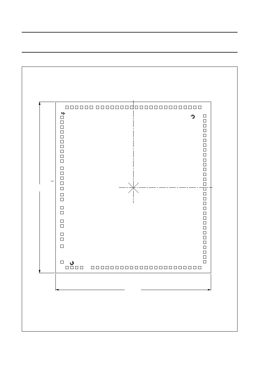
1998 Jul 30
44
Philips Semiconductors
Product specification
LCD controller/driver
PCF2105
18 BONDING PAD LOCATIONS
Fig.30 Bonding pad locations.
Chip dimensions: approximately 5.10
×
5.63 mm.
Gold bump dimensions: approximately 89
×
89
×
25
µ
m.
handbook, full pagewidth
PCF2105
5.63
mm
5.10 mm
x
y
0
0
C58
C57
C56
C55
C54
C59
R21
R20
R19
R18
R17
C60
R22
R24
R23
R29
R5
R32
R31
R30
R6
R8
R7
C17
C18
C19
C20
C21
C22
C16
C10
C11
C12
C13
C14
C15
C9
C7
C8
C6
C2
C3
C4
C5
R11
R12
R14
R13
C1
R10
R9
SA0
V
SS
V
DD
OSC
C35
C36
C37
C38
C39
C40
C41
C42
C43
C44
C45
C46
C48
C49
C47
C50
C51
C23
C24
C25
C26
C27
C28
C29
C31
C32
C30
C33
C34
C52
C53
RS
R/W
T1
DB7
DB6
DB5
DB4
DB3
DB2
DB1
DB0
SDA
VLCD
R15
R16
R25
R26
R27
R28
R1
R3
R4
R2
SCL
E
1
2
3
4
5
6
7
8
9
10 11 12 13 14 15 16 17 18 19 20 21 22 23 24 25 26 27
86
59
60
61
62
63
64
65
66
67
68
69
70
71
72
73
74
75
76
77
78
79
80
81
82
83
84
85
28
29
30
31
32
33
34
35
37
38
39
40
41
42
43
44
45
46
47
48
49
50
51
52
53
54
55
56
57
58
36
87
88
89
90
91
92
93
94
95
96
97
98
99
100
101
102
103
104
105
106
107
108
109
110
111
MGK857

1998 Jul 30
45
Philips Semiconductors
Product specification
LCD controller/driver
PCF2105
Table 12 Bonding pad locations (dimensions in
µ
m).
All x/y coordinates are referenced to centre of chip,
see Fig.30.
SYMBOL
PAD
x
y
OSC
1
-
2184.5
-
2637
V
DD
2
-
2024.5
-
2637
SA0
3
-
1864.5
-
2637
V
SS
4
-
1704.5
-
2637
R8
5
-
1339
-
2637
R7
6
-
1179
-
2637
R6
7
-
1019
-
2637
R5
8
-
859
-
2637
R32
9
-
699
-
2637
R31
10
-
539
-
2637
R30
11
-
379
-
2637
R29
12
-
219
-
2637
R24
13
-
59
-
2637
R23
14
101
-
2637
R22
15
261
-
2637
R21
16
421
-
2637
R20
17
581
-
2637
R19
18
741
-
2637
R18
19
901
-
2637
R17
20
1061
-
2637
C60
21
1221
-
2637
C59
22
1381
-
2637
C58
23
1541
-
2637
C57
24
1701
-
2637
C56
25
1861
-
2637
C55
26
2021
-
2637
C54
27
2181
-
2637
C53
28
2350
-
2445
C52
29
2350
-
2285
C51
30
2350
-
2125
C50
31
2350
-
1965
C49
32
2350
-
1805
C48
33
2350
-
1645
C47
34
2350
-
1485
C46
35
2350
-
1325
C45
36
2350
-
1165
C44
37
2350
-
1005
C43
38
2350
-
845
C42
39
2350
-
685
C41
40
2350
-
525
C40
41
2350
-
365
C39
42
2350
-
205
C38
43
2350
-
45
C37
44
2350
115
C36
45
2350
275
C35
46
2350
435
C34
47
2350
595
C33
48
2350
755
C32
49
2350
915
C31
50
2350
1075
C30
51
2350
1235
C29
52
2350
1395
C28
53
2350
1555
C27
54
2350
1715
C26
55
2350
1875
C25
56
2350
2035
C24
57
2350
2195
C23
58
2350
2355
C22
59
2185
2637.5
C21
60
2025
2637.5
C20
61
1865
2637.5
C19
62
1705
2637.5
C18
63
1545
2637.5
C17
64
1385
2637.5
C16
65
1225
2637.5
C15
66
1065
2637.5
C14
67
905
2637.5
C13
68
745
2637.5
C12
69
585
2637.5
C11
70
425
2637.5
C10
71
265
2637.5
C9
72
105
2637.5
C8
73
-
55
2637.5
C7
74
-
215
2637.5
C6
75
-
375
2637.5
C5
76
-
535
2637.5
SYMBOL
PAD
x
y

1998 Jul 30
46
Philips Semiconductors
Product specification
LCD controller/driver
PCF2105
C4
77
-
695
2637.5
C3
78
-
855
2637.5
C2
79
-
1015
2637.5
C1
80
-
1175
2637.5
R9
81
-
1385
2637.5
R10
82
-
1545
2637.5
R11
83
-
1705
2637.5
R12
84
-
1865
2637.5
R13
85
-
2025
2637.5
R14
86
-
2185
2637.5
R15
87
-
2349
2308
R16
88
-
2349
2148
R25
89
-
2349
1988
R26
90
-
2349
1828
R27
91
-
2349
1668
R28
92
-
2349
1508
R1
93
-
2349
1348
R2
94
-
2349
1188
R3
95
-
2349
1028
R4
96
-
2349
868
SCL
97
-
2349
632
E
98
-
2349
472
RS
99
-
2349
312
R/W
100
-
2349
142
T1
101
-
2349
-
34
DB7
102
-
2349
-
233
DB6
103
-
2349
-
393
DB5
104
-
2349
-
668
DB4
105
-
2349
-
828
DB3
106
-
2349
-
1103
DB2
107
-
2349
-
1263
DB1
108
-
2349
-
1538
DB0
109
-
2349
-
1698
SDA
110
-
2349
-
1933
V
LCD
111
-
2349
-
2453
RECPAT `F'
-
-
2327.5
2427.5
RECPAT `C'
-
-
2027.5
-
2512.5
RECPAT `C'
-
1982.5
2297.5
SYMBOL
PAD
x
y

1998 Jul 30
47
Philips Semiconductors
Product specification
LCD controller/driver
PCF2105
19 DEFINITIONS
20 LIFE SUPPORT APPLICATIONS
These products are not designed for use in life support appliances, devices, or systems where malfunction of these
products can reasonably be expected to result in personal injury. Philips customers using or selling these products for
use in such applications do so at their own risk and agree to fully indemnify Philips for any damages resulting from such
improper use or sale.
21 PURCHASE OF PHILIPS I
2
C COMPONENTS
Data sheet status
Objective specification
This data sheet contains target or goal specifications for product development.
Preliminary specification
This data sheet contains preliminary data; supplementary data may be published later.
Product specification
This data sheet contains final product specifications.
Limiting values
Limiting values given are in accordance with the Absolute Maximum Rating System (IEC 134). Stress above one or
more of the limiting values may cause permanent damage to the device. These are stress ratings only and operation
of the device at these or at any other conditions above those given in the Characteristics sections of the specification
is not implied. Exposure to limiting values for extended periods may affect device reliability.
Application information
Where application information is given, it is advisory and does not form part of the specification.
Purchase of Philips I
2
C components conveys a license under the Philips' I
2
C patent to use the
components in the I
2
C system provided the system conforms to the I
2
C specification defined by
Philips. This specification can be ordered using the code 9398 393 40011.

Internet: http://www.semiconductors.philips.com
Philips Semiconductors a worldwide company
© Philips Electronics N.V. 1998
SCA60
All rights are reserved. Reproduction in whole or in part is prohibited without the prior written consent of the copyright owner.
The information presented in this document does not form part of any quotation or contract, is believed to be accurate and reliable and may be changed
without notice. No liability will be accepted by the publisher for any consequence of its use. Publication thereof does not convey nor imply any license
under patent- or other industrial or intellectual property rights.
Middle East: see Italy
Netherlands: Postbus 90050, 5600 PB EINDHOVEN, Bldg. VB,
Tel. +31 40 27 82785, Fax. +31 40 27 88399
New Zealand: 2 Wagener Place, C.P.O. Box 1041, AUCKLAND,
Tel. +64 9 849 4160, Fax. +64 9 849 7811
Norway: Box 1, Manglerud 0612, OSLO,
Tel. +47 22 74 8000, Fax. +47 22 74 8341
Pakistan: see Singapore
Philippines: Philips Semiconductors Philippines Inc.,
106 Valero St. Salcedo Village, P.O. Box 2108 MCC, MAKATI,
Metro MANILA, Tel. +63 2 816 6380, Fax. +63 2 817 3474
Poland: Ul. Lukiska 10, PL 04-123 WARSZAWA,
Tel. +48 22 612 2831, Fax. +48 22 612 2327
Portugal: see Spain
Romania: see Italy
Russia: Philips Russia, Ul. Usatcheva 35A, 119048 MOSCOW,
Tel. +7 095 755 6918, Fax. +7 095 755 6919
Singapore: Lorong 1, Toa Payoh, SINGAPORE 319762,
Tel. +65 350 2538, Fax. +65 251 6500
Slovakia: see Austria
Slovenia: see Italy
South Africa: S.A. PHILIPS Pty Ltd., 195-215 Main Road Martindale,
2092 JOHANNESBURG, P.O. Box 7430 Johannesburg 2000,
Tel. +27 11 470 5911, Fax. +27 11 470 5494
South America: Al. Vicente Pinzon, 173, 6th floor,
04547-130 SĂO PAULO, SP, Brazil,
Tel. +55 11 821 2333, Fax. +55 11 821 2382
Spain: Balmes 22, 08007 BARCELONA,
Tel. +34 93 301 6312, Fax. +34 93 301 4107
Sweden: Kottbygatan 7, Akalla, S-16485 STOCKHOLM,
Tel. +46 8 5985 2000, Fax. +46 8 5985 2745
Switzerland: Allmendstrasse 140, CH-8027 ZÜRICH,
Tel. +41 1 488 2741 Fax. +41 1 488 3263
Taiwan: Philips Semiconductors, 6F, No. 96, Chien Kuo N. Rd., Sec. 1,
TAIPEI, Taiwan Tel. +886 2 2134 2865, Fax. +886 2 2134 2874
Thailand: PHILIPS ELECTRONICS (THAILAND) Ltd.,
209/2 Sanpavuth-Bangna Road Prakanong, BANGKOK 10260,
Tel. +66 2 745 4090, Fax. +66 2 398 0793
Turkey: Talatpasa Cad. No. 5, 80640 GÜLTEPE/ISTANBUL,
Tel. +90 212 279 2770, Fax. +90 212 282 6707
Ukraine: PHILIPS UKRAINE, 4 Patrice Lumumba str., Building B, Floor 7,
252042 KIEV, Tel. +380 44 264 2776, Fax. +380 44 268 0461
United Kingdom: Philips Semiconductors Ltd., 276 Bath Road, Hayes,
MIDDLESEX UB3 5BX, Tel. +44 181 730 5000, Fax. +44 181 754 8421
United States: 811 East Arques Avenue, SUNNYVALE, CA 94088-3409,
Tel. +1 800 234 7381
Uruguay: see South America
Vietnam: see Singapore
Yugoslavia: PHILIPS, Trg N. Pasica 5/v, 11000 BEOGRAD,
Tel. +381 11 625 344, Fax.+381 11 635 777
For all other countries apply to: Philips Semiconductors,
International Marketing & Sales Communications, Building BE-p, P.O. Box 218,
5600 MD EINDHOVEN, The Netherlands, Fax. +31 40 27 24825
Argentina: see South America
Australia: 34 Waterloo Road, NORTH RYDE, NSW 2113,
Tel. +61 2 9805 4455, Fax. +61 2 9805 4466
Austria: Computerstr. 6, A-1101 WIEN, P.O. Box 213, Tel. +43 160 1010,
Fax. +43 160 101 1210
Belarus: Hotel Minsk Business Center, Bld. 3, r. 1211, Volodarski Str. 6,
220050 MINSK, Tel. +375 172 200 733, Fax. +375 172 200 773
Belgium: see The Netherlands
Brazil: see South America
Bulgaria: Philips Bulgaria Ltd., Energoproject, 15th floor,
51 James Bourchier Blvd., 1407 SOFIA,
Tel. +359 2 689 211, Fax. +359 2 689 102
Canada: PHILIPS SEMICONDUCTORS/COMPONENTS,
Tel. +1 800 234 7381
China/Hong Kong: 501 Hong Kong Industrial Technology Centre,
72 Tat Chee Avenue, Kowloon Tong, HONG KONG,
Tel. +852 2319 7888, Fax. +852 2319 7700
Colombia: see South America
Czech Republic: see Austria
Denmark: Prags Boulevard 80, PB 1919, DK-2300 COPENHAGEN S,
Tel. +45 32 88 2636, Fax. +45 31 57 0044
Finland: Sinikalliontie 3, FIN-02630 ESPOO,
Tel. +358 9 615800, Fax. +358 9 61580920
France: 51 Rue Carnot, BP317, 92156 SURESNES Cedex,
Tel. +33 1 40 99 6161, Fax. +33 1 40 99 6427
Germany: Hammerbrookstraße 69, D-20097 HAMBURG,
Tel. +49 40 23 53 60, Fax. +49 40 23 536 300
Greece: No. 15, 25th March Street, GR 17778 TAVROS/ATHENS,
Tel. +30 1 4894 339/239, Fax. +30 1 4814 240
Hungary: see Austria
India: Philips INDIA Ltd, Band Box Building, 2nd floor,
254-D, Dr. Annie Besant Road, Worli, MUMBAI 400 025,
Tel. +91 22 493 8541, Fax. +91 22 493 0966
Indonesia: PT Philips Development Corporation, Semiconductors Division,
Gedung Philips, Jl. Buncit Raya Kav.99-100, JAKARTA 12510,
Tel. +62 21 794 0040 ext. 2501, Fax. +62 21 794 0080
Ireland: Newstead, Clonskeagh, DUBLIN 14,
Tel. +353 1 7640 000, Fax. +353 1 7640 200
Israel: RAPAC Electronics, 7 Kehilat Saloniki St, PO Box 18053,
TEL AVIV 61180, Tel. +972 3 645 0444, Fax. +972 3 649 1007
Italy: PHILIPS SEMICONDUCTORS, Piazza IV Novembre 3,
20124 MILANO, Tel. +39 2 6752 2531, Fax. +39 2 6752 2557
Japan: Philips Bldg 13-37, Kohnan 2-chome, Minato-ku,
TOKYO 108-8507, Tel. +81 3 3740 5130, Fax. +81 3 3740 5077
Korea: Philips House, 260-199 Itaewon-dong, Yongsan-ku, SEOUL,
Tel. +82 2 709 1412, Fax. +82 2 709 1415
Malaysia: No. 76 Jalan Universiti, 46200 PETALING JAYA, SELANGOR,
Tel. +60 3 750 5214, Fax. +60 3 757 4880
Mexico: 5900 Gateway East, Suite 200, EL PASO, TEXAS 79905,
Tel. +9-5 800 234 7381
Printed in The Netherlands
415106/1200/02/pp48
Date of release: 1998 Jul 30
Document order number:
9397 750 04198