Document Outline
- CONTENTS
- 1 FEATURES
- 2 GENERAL DESCRIPTION
- 3 QUICK REFERENCE DATA
- 4 ORDERING INFORMATION
- 5 BLOCK DIAGRAM
- 6 PINNING
- 7 FUNCTIONAL DESCRIPTION
- 7.1 Power supply (VDD and VSS )
- 7.2 Clock oscillator (OSCI and OSCO)
- 7.3 Chip enable (CE)
- 7.4 Mode selection (PD/DTMF)
- 7.5 Keyboard inputs/outputs
- 7.6 Flash duration control (FLD)
- 7.7 TONE output (DTMF mode)
- 7.8 Dial pulse and Flash output (DP/FLO)
- 7.9 Mute output (M1)
- 7.10 Mute output (M1)
- 7.11 Muting output (M2)
- 8 DIALLING PROCEDURES
- 8.1 Dialling
- 8.2 Redialling
- 8.3 Notepad
- 9 HANDLING
- 10 LIMITING VALUES
- 11 CHARACTERISTICS
- 12 TIMING CHARACTERISTICS
- 13 APPLICATION INFORMATION
- 14 PACKAGE OUTLINES
- 15 SOLDERING
- 16 DEFINITIONS
DATA SHEET
Product specification
Supersedes data of 1996 May 06
File under Integrated Circuits, IC03
1996 Nov 21
INTEGRATED CIRCUITS
PCD3310; PCD3310A
Pulse and DTMF diallers with redial

1996 Nov 21
2
Philips Semiconductors
Product specification
Pulse and DTMF diallers with redial
PCD3310; PCD3310A
CONTENTS
1
FEATURES
2
GENERAL DESCRIPTION
3
QUICK REFERENCE DATA
4
ORDERING INFORMATION
5
BLOCK DIAGRAM
6
PINNING
7
FUNCTIONAL DESCRIPTION
7.1
Power supply (V
DD
and V
SS
)
7.2
Clock oscillator (OSCI and OSCO)
7.3
Chip enable (CE)
7.4
Mode selection (PD/DTMF)
7.4.1
Pulse mode
7.4.2
DTMF mode
7.4.3
Mixed mode
7.5
Keyboard inputs/outputs
7.6
Flash duration control (FLD)
7.7
TONE output (DTMF mode)
7.8
Dial pulse and Flash output (DP/FLO)
7.9
Mute output (M1)
7.10
Mute output (M1)
7.11
Muting output (M2)
8
DIALLING PROCEDURES
8.1
Dialling
8.2
Redialling
8.3
Notepad
9
HANDLING
10
LIMITING VALUES
11
CHARACTERISTICS
12
TIMING CHARACTERISTICS
13
APPLICATION INFORMATION
14
PACKAGE OUTLINES
15
SOLDERING
15.1
Introduction
15.2
DIP
15.2.1
Soldering by dipping or by wave
15.2.2
Repairing soldered joints
15.3
SO
15.3.1
Reflow soldering
15.3.2
Wave soldering
15.3.3
Repairing soldered joints
16
DEFINITIONS
17
LIFE SUPPORT APPLICATIONS
1996 Nov 21
3
Philips Semiconductors
Product specification
Pulse and DTMF diallers with redial
PCD3310; PCD3310A
1
FEATURES
·
Pulse, DTMF and `mixed mode' dialling
·
Mixed mode dialling: start with pulse dial, end with
DTMF dial (e.g. for control of DTMF user equipment via
a pulse network)
·
23-digit memory stores last number dialled, or number
noted during conversation (notepad)
·
Redial of both PABX and external calls
·
Supports 16 dial keys: 0 to 9,
, # A, B, C, and D
·
Supports 4 function keys:
Program (P) used to input notepad numbers
Flash (FL) allows re-dialling without on-hook
Redial (R) recalls and redialls stored number
Change from pulse dial to DTMF dial in
mixed mode (>)
·
DTMF timing:
for manual dialling, maximum duration burst/pause
intervals are user-determined, but at least minimum
duration burst/pause intervals are ensured
for redial, minimum duration burst/pause intervals are
used
·
On-chip voltage reference for supply and temperature
independent tone output
·
On-chip filtering for low output distortion
(CEPT compatible)
·
On-chip oscillator uses low-cost 3.58 MHz (TV colour
burst) crystal or piezo resonator
·
Uses standard single-contact or double-contact
(common left open) keyboard
·
Keyboard entries fully debounced
·
Flash (register recall) output.
2
GENERAL DESCRIPTION
The PCD3310 and PCD3310A are single-chip silicon gate
CMOS integrated circuits. They are dual-standard diallers
for pulse or dual tone multi-frequency (DTMF) dialling, with
on-chip oscillators suitable for use with 3.58 MHz crystals.
Input data is derived from any standard matrix keyboard
for dialling in either the pulse or DTMF mode.
Numbers up to 23 digits can be retained in RAM for
dialling/redialling.
3
QUICK REFERENCE DATA
SYMBOL
PARAMETER
CONDITIONS
MIN.
TYP.
MAX.
UNIT
V
DD
operating supply voltage
2.5
-
6.0
V
V
stb
standby supply voltage
1.8
-
6.0
V
I
DD(stb)
standby current (on hook)
V
stb
= 1.8 V
-
1.4
4
µ
A
I
DD(conv)
operating current in conversation mode
V
DD
= 3 V
-
-
150
µ
A
I
DD(pulse)
operating current in pulse dialling mode
V
DD
= 3 V
-
-
200
µ
A
I
DD(DTMF)
operating current in DTMF dialling mode
V
DD
= 3 V
-
0.6
0.9
mA
V
HG(RMS)
DTMF output voltage level for HIGH group
(RMS value)
-
192
-
mV
V
LG(RMS)
DTMF output voltage level for LOW group
(RMS value)
-
150
-
mV
G
v
voltage gain (pre-emphasis) of group
-
2.1
-
dB
THD
total harmonic distortion
-
-
25
-
dB
T
amb
operating ambient temperature
-
25
-
+70
°
C
1996 Nov 21
4
Philips Semiconductors
Product specification
Pulse and DTMF diallers with redial
PCD3310; PCD3310A
4
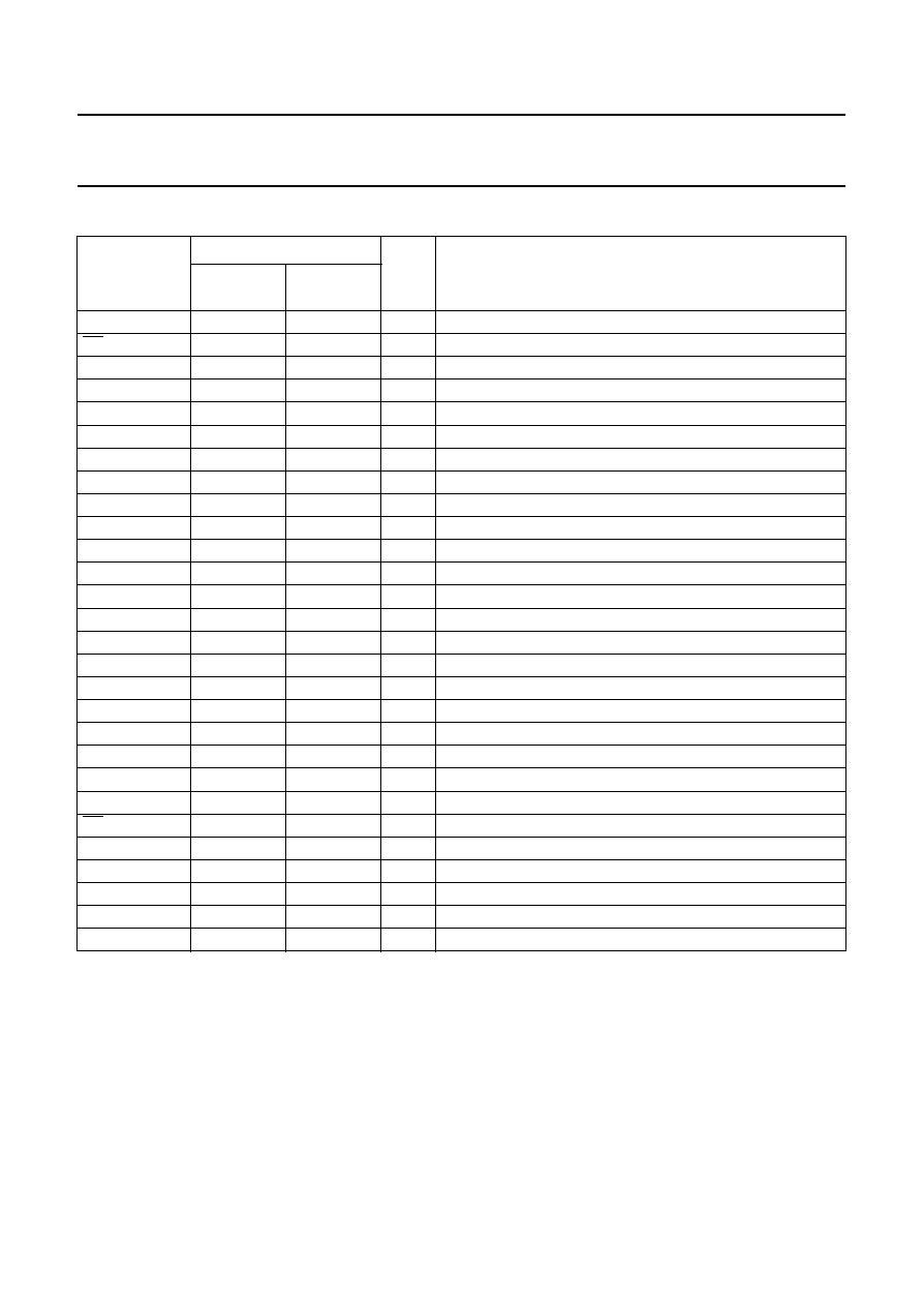
ORDERING INFORMATION
Table 1
Package information
Table 2
Functional options
Notes
1. Pulse frequency 10 Hz, inter-digit pause (t
id
) = 840 ms.
2. Note that the PCD3310P; 10T and the PCD3310AP; 10AT differ only in the break/make ratio in pulse dialling.
The break/make times equate to mark-to-space ratios of 2 : 1 and 3 : 2 respectively.
TYPE
NUMBER
PACKAGE
NAME
DESCRIPTION
VERSION
PCD3310P
DIP20
plastic dual in-line package; 20 leads (300 mil)
SOT146-1
PCD3310AP
DIP20
plastic dual in-line package; 20 leads (300 mil)
SOT146-1
PCD3310T
SO28
plastic small outline package; 28 leads; body width 7.5 mm
SOT136-1
PCD3310AT
SO28
plastic small outline package; 28 leads; body width 7.5 mm
SOT136-1
TYPE
NUMBER
PULSE DIAL; BREAK/MAKE TIME (see notes 1 and 2)
MARK-TO-SPACE
RATIO
PCD3310P
67, 33 ms
2 : 1
PCD3310T
67, 33 ms
2 : 1
PCD3310AP
60, 40 ms
3 : 2
PCD3310AT
60, 40 ms
3 : 2
1996 Nov 21
5
Philips Semiconductors
Product specification
Pulse and DTMF diallers with redial
PCD3310; PCD3310A
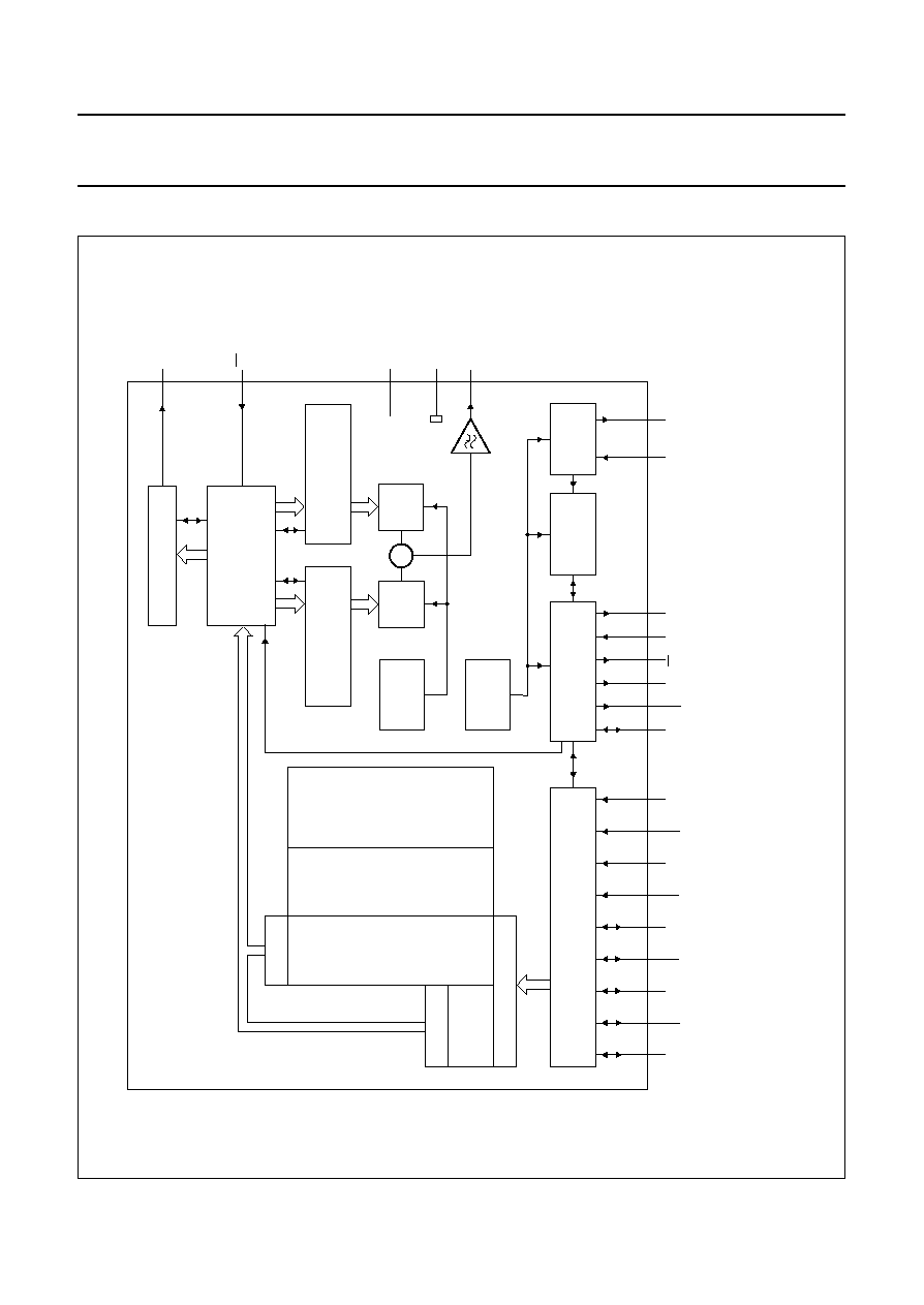
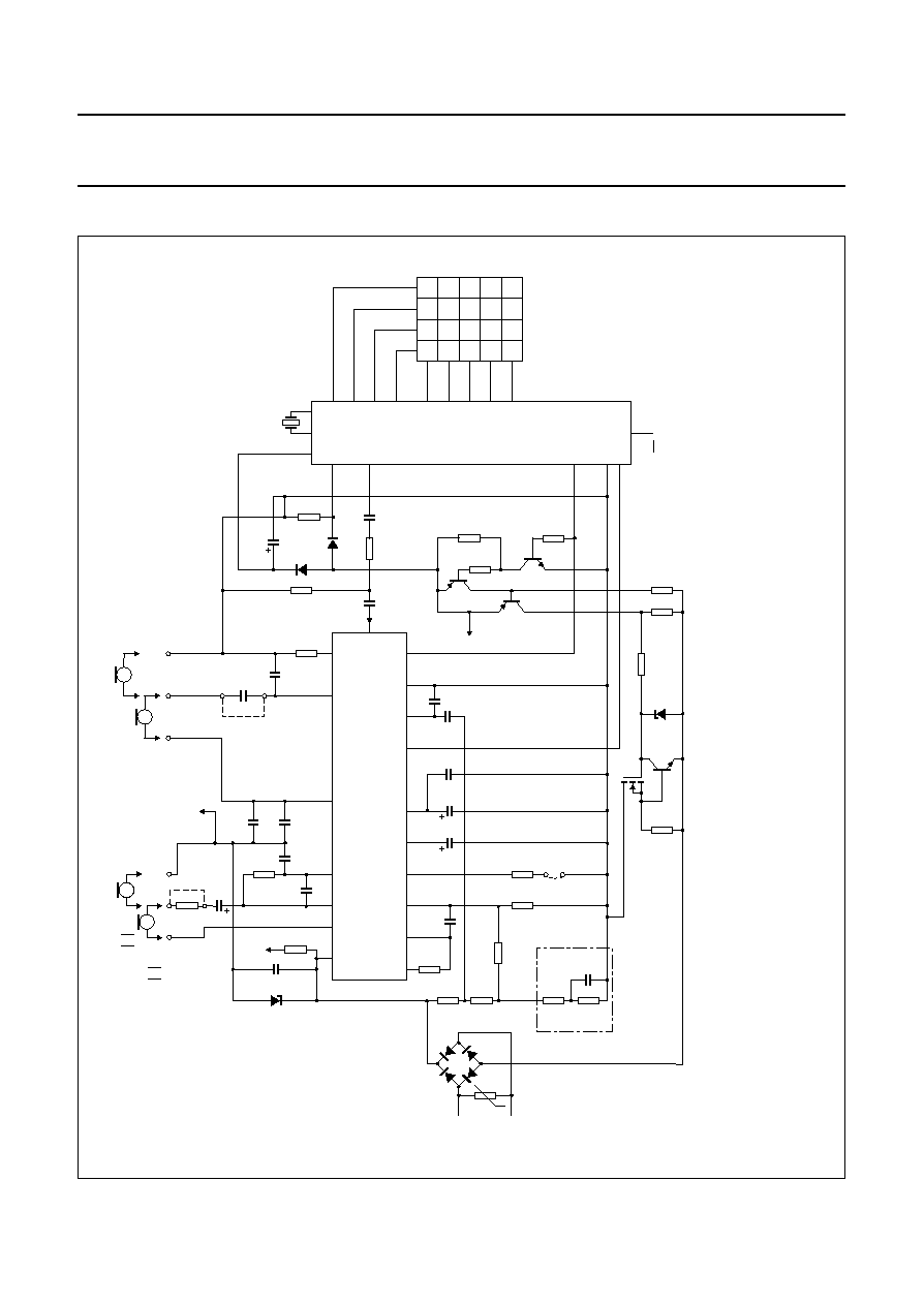
5
BLOCK DIAGRAM
Fig.1 Block diagram.
The pin numbers given in parenthesis refer to the PCD3310T.
handbook, full pagewidth
MGE490
PD AND FLASH LOGIC
PD
CODE CONVERTER
TIMING CONTROLLER
DTMF
DTMF HIGH GROUP
COUNTER/CONTROLLER
DTMF LOW GROUP
COUNTER/CONTROLLER
VOLTAGE
REFERENCE
V
ref
DAC
HIGH
DAC
LOW
POWER
ON
RESET
TIME BASE
RESET DELAY
COUNTER
OSCILLATOR
CONTROL
LOGIC
COUNTER
POINTER
CONTROLLER
ADDRESS
DECODING
MAIN
REGISTER
OUTPUT
OUTPUT
TEMPORARY
REGISTER
INPUT
KEYPAD
INTERFACE
/
LOGIC
(9)
6
(10)
7
(12)
8
(13)
9
(14)
10
(15)
11
(16)
12
(17)
13
(19)
14
(8)
5
(20)
15
(24)
17
(26)
18
(22)
(1)
1
(28)
20
(3)
3
(5)
4
(27)
19
(2)
2
(21)
16
DP/FLO
PD/DTMF
V
DD
V
SS
TONE
ROW 5
ROW 4
ROW 3
ROW 2
ROW 1
COL 1
COL 2
COL 3
COL 4
FLD
CF/DMODE/FS
M1
M1
(23)
CE
M2
OSCO
OSCI
PCD3310 FAMILY
READ/
WRITE
+
1996 Nov 21
6
Philips Semiconductors
Product specification
Pulse and DTMF diallers with redial
PCD3310; PCD3310A
6
PINNING
SYMBOL
PINS
TYPE
DESCRIPTION
PCD3310P
PCD3310AP
PCD3310T
PCD3310AT
OSCI
1
1
I
oscillator input
PD/DTMF
2
2
I
select pin; pulse or DTMF dialling input
TONE
3
3
O
single or dual tone frequency output
n.c.
-
4
-
not connected
V
SS
4
5
P
negative supply
n.c.
-
6
-
not connected
n.c.
-
7
-
not connected
FLD
5
8
I/O
flash duration control input/output
ROW 5
6
9
I/O
scanning row 5 keyboard input/output
ROW 4
7
10
I/O
scanning row 4 keyboard input/output
n.c.
-
11
-
not connected
ROW 3
8
12
I/O
scanning row 3 keyboard input/output
ROW 2
9
13
I/O
scanning row 2 keyboard input/output
ROW 1
10
14
I/O
scanning row 1 keyboard input/output
COL 1
11
15
I
sense column 1 keyboard input (with internal pull-up resistor)
COL 2
12
16
I
sense column 2 keyboard input (with internal pull-up resistor)
COL 3
13
17
I
sense column 3 keyboard input (with internal pull-up resistor)
n.c.
-
18
-
not connected
COL 4
14
19
I
sense column 4 keyboard input (with internal pull-up resistor)
CF/DMODE/FS
15
20
O
confidence tone/dialling mode/frequency select outputs
DP/FLO
16
21
O
dialling pulse and flash output
M2
-
22
O
muting output 2
M1
-
23
O
muting output 1 (active LOW)
M1
17
24
O
muting output 1
n.c.
-
25
-
not connected
CE
18
26
I
chip enable input
V
DD
19
27
P
positive supply voltage
OSCO
20
28
O
oscillator output
1996 Nov 21
7
Philips Semiconductors
Product specification
Pulse and DTMF diallers with redial
PCD3310; PCD3310A
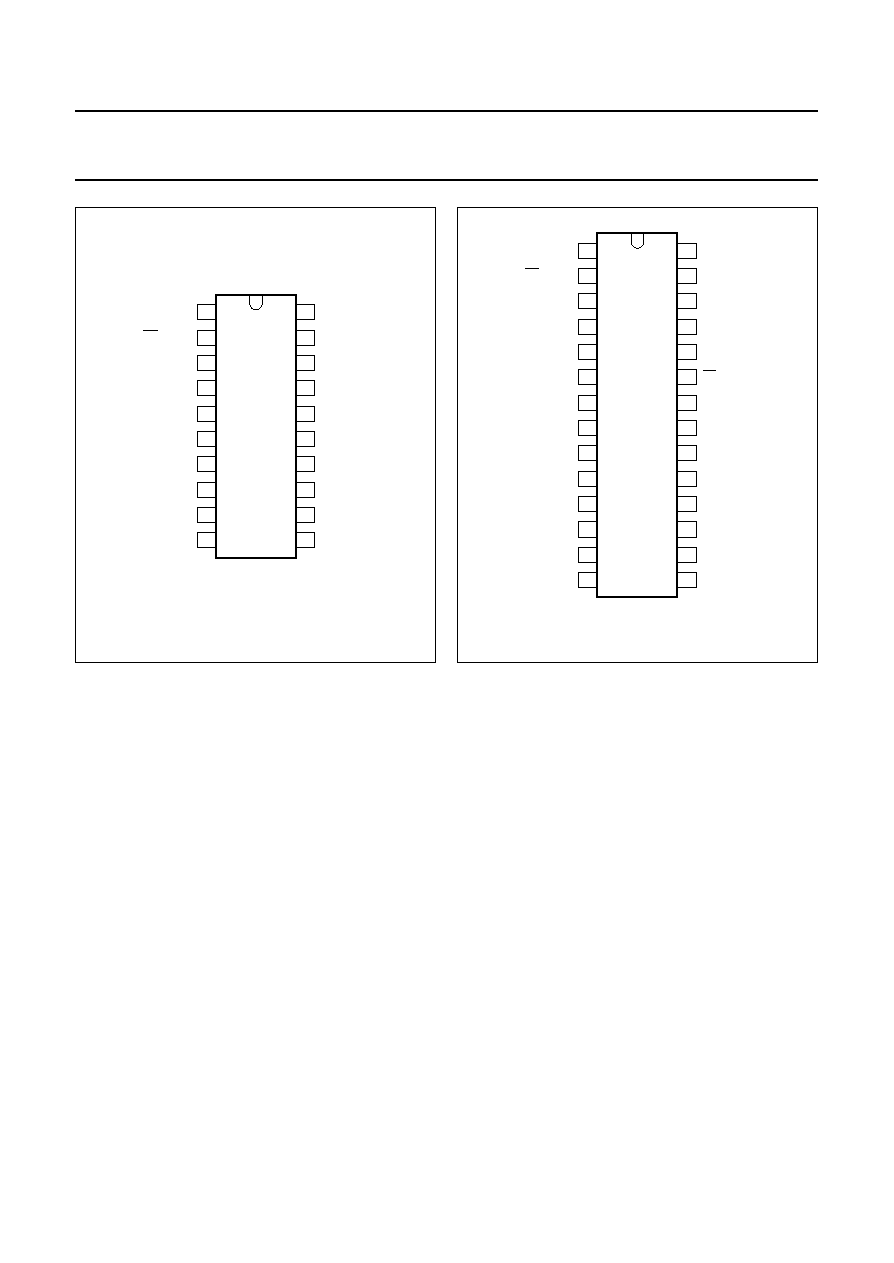
Fig.2 Pin configuration (DIP20 package).
handbook, halfpage
OSCI
PD/DTMF
TONE
VSS
FLD
ROW 5
ROW 4
ROW 3
ROW 2
ROW 1
OSCO
VDD
CE
M1
CF/DMODE/FS
COL 4
DP/FLO
COL 3
COL 2
COL 1
1
2
3
4
5
6
7
8
9
10
11
12
20
19
18
17
16
15
14
13
PCD3310P
PCD3310AP
MGE489
Fig.3 Pin configuration (SO28 package).
handbook, halfpage
OSCI
PD/DTMF
TONE
n.c.
VSS
n.c.
n.c.
FLD
ROW 5
ROW 4
n.c.
ROW 3
ROW 2
ROW 1
OSCO
VDD
CE
n.c.
M1
M2
M1
DP/FLO
CF/DMODE/FS
COL 4
n.c.
COL 3
COL 2
COL 1
1
2
3
4
5
6
7
8
9
10
11
12
13
28
27
26
25
24
23
22
21
20
19
18
17
16
15
14
PCD3310T
PCD3310AT
MGE488
7
FUNCTIONAL DESCRIPTION
References to `the device' apply to both the PCD3310 and
the PCD3310A.
7.1
Power supply (V
DD
and V
SS
)
The positive supply of the device (V
DD
) must meet the
voltage requirements as indicated in Chapter 11.
To avoid undefined states of the device at power-on, an
internal reset circuit clears the control logic and counters.
If V
DD
drops below the minimum standby supply voltage of
1.8 V the power-on reset circuit inhibits redialling after
hook-off. The power-on reset signal has the highest
priority; it blocks and resets the device without delay
regardless of the state of chip enable input (CE).
7.2
Clock oscillator (OSCI and OSCO)
The timebase for the device for both pulse and DTMF
dialling is a crystal controlled on-chip oscillator which is
completed by connecting a 3.58 MHz crystal or ceramic
resonator between the OSCI and OSCO pins.
Recommended resonator type:
·
3.58 MHz PXE - Murata; CSA 3.58MG310VA.
7.3
Chip enable (CE)
The CE input enables the device and is used to initialize
the device. When CE is LOW it provides the static standby
condition. In this state the clock oscillator is disabled, all
registers and logic are reset with the exception of the redial
registers, Read Address Counter (RAC), Write Address
Counter (WAC) and Temporary Write Address Counter
(TWAC). The RAC points to the first digit of the last
number dialled, the WAC and TWAC point to the last
entered digits in the main and temporary registers
(see Fig.6). The keyboard input is inhibited, but data
previously entered is saved in the redial registers provided
V
DD
is higher than V
stb
. The current drawn is I
stb
(standby
current) and serves to retain data in the redial registers
during hook-on.
When CE is HIGH it activates the clock oscillator and the
device changes from static standby condition to the
conversation mode. The current consumption is I
DD(conv)
until the first digit is entered from the keyboard. Then a
dialling or redialling operation starts. The operating current
is I
DD(pulse)
if in the pulse dialling mode, or I
DD(DTMF)
if the
DTMF dialling mode is selected.

1996 Nov 21
8
Philips Semiconductors
Product specification
Pulse and DTMF diallers with redial
PCD3310; PCD3310A
If the CE input is taken to a LOW level for longer than time
period t
rd
(see Figs 11 and 12 and Chapter 12) an internal
reset pulse will be generated at the end of the t
rd
period.
The system changes to the static standby state. Short CE
pulses of < t
rd
will not affect the operation of the device and
reset pulses are not produced.
7.4
Mode selection (PD/DTMF)
7.4.1
P
ULSE MODE
If PD/DTMF = V
SS
the pulse mode is selected. Entries of
non-numeric keys are neglected, they are neither stored in
the redial register nor transmitted.
7.4.2
DTMF
MODE
If PD/DTMF = V
DD
the dual tone multi-frequency dialling
mode is selected. Each non-function key activated
corresponds to a combination of two tones, one of four
LOW and one of four HIGH frequencies, corresponding to
the key's row and column in the keyboard matrix.
See Fig.4 and Table 3. The frequencies are transmitted
with a constant amplitude, regardless of power supply
variations. Harmonic content is filtered out thus meeting
the CEPT recommendations.
The transmission time is calibrated for redial. In manual
operation the duration of bursts and pauses is the actual
key depression time, but not less than the minimum
transmission time (t
t
) or minimum pause time (t
p
).
7.4.3
M
IXED MODE
When the PD/DTMF pin is open-circuit the mixed mode is
selected. After activation of CE or FL (Flash) the device
starts as a pulse dialler and remains in this state until a
non-numeric dial key (A, B, C, D,
, #) or the function key >
is activated. Pressing a non-numeric dial key causes the
corresponding DTMF tones to be output, and any
subsequent dialling to be in DTMF mode. Pressing >
causes no output tones, but any subsequent dialling is in
DTMF mode. The > key should be used if the first DTMF
output required is numeric. The device remains in DTMF
dial mode until FL is activated or after a static standby
condition when CE is re-activated.
A connection between the PD/DTMF pin and V
DD
also
initiates DTMF dialling. Chip enable, FL or a connection of
PD/DTMF pin to V
SS
sets the device back to pulse dialling.
7.5
Keyboard inputs/outputs
The sense column inputs COL 1 to COL 4 and the
scanning row outputs ROW 1 to ROW 5 of the device are
connected to the keyboard as shown in Fig.4. All keyboard
entries are debounced on both the leading and trailing
edges for approximately time period t
e
as shown in
Figs 11, 12, 13 and 14. Each entry is tested for validity.
When a key is depressed, keyboard scanning starts and
only returns to the sense mode after release of that key.
ROW 5 of the keyboard contains the following function
keys:
·
P = memory clear and programming (notepad)
·
FL = flash or register recall
·
R = redial
·
> = change of dial mode from pulse to DTMF in mixed
dialling mode.
In the pulse dialling mode the valid keys are the
10 numeric dial keys (0 to 9). The non-numeric dial keys
(A, B, C, D,
, #) have no effect on the dialling or the redial
storage. Valid function keys are P, R and FL.
In the DTMF mode all dial keys are valid. They are
transmitted as a dual tone combination and at the same
time stored in the redial register. Valid function keys are P,
FL and R.
In the mixed mode all key entries are valid and executed
accordingly.
Fig.4 Keyboard organization.
handbook, halfpage
MGE491
1
2
3
4
5
6
7
8
9
0
#
P
FL
R
A
B
C
D
>
ROWS
COLUMNS
KEYBOARD
5
4
3
2
1
1
2
3
4
1996 Nov 21
9
Philips Semiconductors
Product specification
Pulse and DTMF diallers with redial
PCD3310; PCD3310A
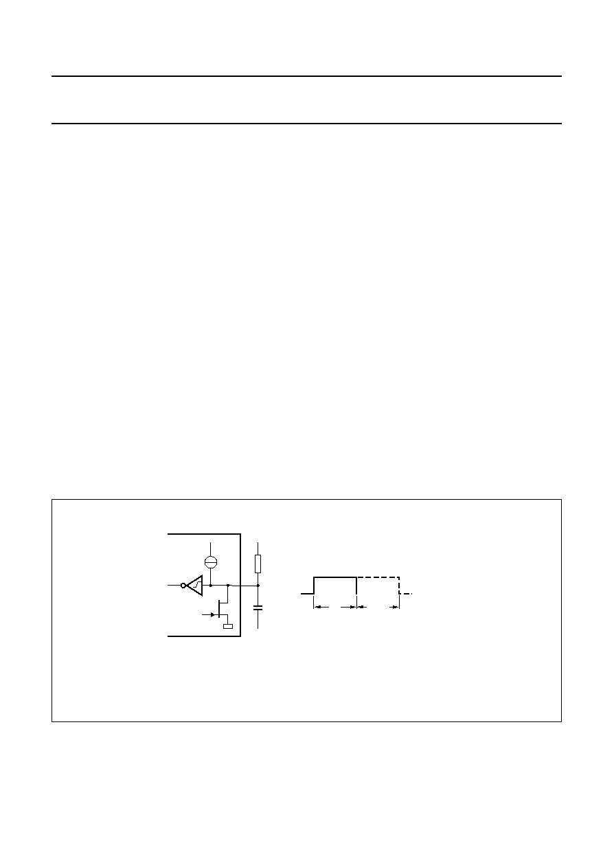
7.6
Flash duration control (FLD)
Flash (or register recall) is activated by the FL key and can
be used in DTMF and pulse dialling modes.
The FL key has the same effect as placing the telephone
`on-hook' for a calibrated time. Pressing the FL key will
produce a timed line-break of 100 ms (min.) at the DP/FLO
output. During the conversation mode pressing FL also
acts as a chip enable. The flash pulse duration (t
FL
) is
calibrated and can be prolonged with an external resistor
and capacitor connected to the FLD input/output (see
Fig.5). The flash pulse resets the Read Address Counter
(RAC) to the address of the first entered digit of the last
number dialled. Subsequent redial is possible (see Fig.9).
The counter of the reset delay time is held for a period of
t
FL
.
7.7
TONE output (DTMF mode)
The single and dual tones which are provided at the TONE
output are filtered by an on-chip switched capacitor filter,
followed by an on-chip active RC low-pass filter. Hence,
the total harmonic distortion of the DTMF tones meets the
CEPT recommendations. The tone output has the
following states:
·
tone OFF; 3-state
·
tone ON; the associated frequencies are superimposed
on a DC level of
1
/
2
V
DD
.
When the DTMF mode is selected output tones are timed
in manual dialling with a minimum duration of bursts and
pauses, and in redial with a calibrated timing. Single tones
may be generated for test purposes (CE = HIGH). Each
row and column has one corresponding frequency.
High group frequencies are generated by connecting the
column to V
SS
and LOW group frequencies are generated
by forcing the row to V
DD
. The single tone frequency will be
transmitted during activation time, but it is neither
calibrated nor stored.
An on-chip reference voltage provides output tone levels
independent of the supply voltage. Table 3 shows the
frequency tolerance of the output tones for DTMF
signalling.
Fig.5 Flash pulse duration setting.
(a) Flash duration control circuit.
(b) Flash pulse timing. t
FLRC
R
×
C.
ndbook, full pagewidth
MGE492
tFL
tFLRC
(a)
(b)
R
C
FLD
60
nA
FLO
1996 Nov 21
10
Philips Semiconductors
Product specification
Pulse and DTMF diallers with redial
PCD3310; PCD3310A
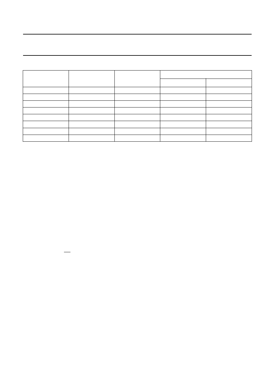
Table 3
Frequency tolerance of the output tones for DTMF signalling; f
xtal
= 3.579545 MHz
ROW/COLUMN
STANDARD
FREQUENCY (Hz)
TONE OUTPUT
FREQUENCY (Hz)
FREQUENCY DEVIATION
%
Hz
ROW 1
697
697.90
+0.13
+0.90
ROW 2
770
770.46
+0.06
+0.46
ROW 3
852
850.45
-
0.18
-
1.55
ROW 4
941
943.23
+0.24
+2.23
COL 1
1209
1206.45
-
0.21
-
2.55
COL 2
1336
1341.66
+0.42
+5.66
COL 3
1477
1482.21
+0.35
+5.21
COL 4
1633
1638.24
+0.32
+5.25
7.8
Dial pulse and Flash output (DP/FLO)
This is a combined output which provides control signals
for timing in pulse dialling or for a calibrated line break
(flash or register recall) in both dialling modes.
7.9
Mute output (M1)
The MUTE output can be used to disable the microphone
during dialling.
During pulse dialling the mute output becomes active
HIGH for the period of the inter-digit pause, break time and
make time. It remains at this level until the last digit is
pulsed out.
During DTMF dialling the mute output becomes active
HIGH for the period of tone transmission and remains at
this level until the end of hold-over time. It is also active
HIGH during flash and flash hold-over time.
7.10
Mute output (M1)
Inverted output of M1. In the PCD3310P it is only available
as a bonding option of M1.
7.11
Muting output (M2)
Active HIGH output during actual dialling; i.e. during break
or make time in pulse dialling, or during tone ON/OFF in
DTMF dialling. It is an open drain p-channel output.
8
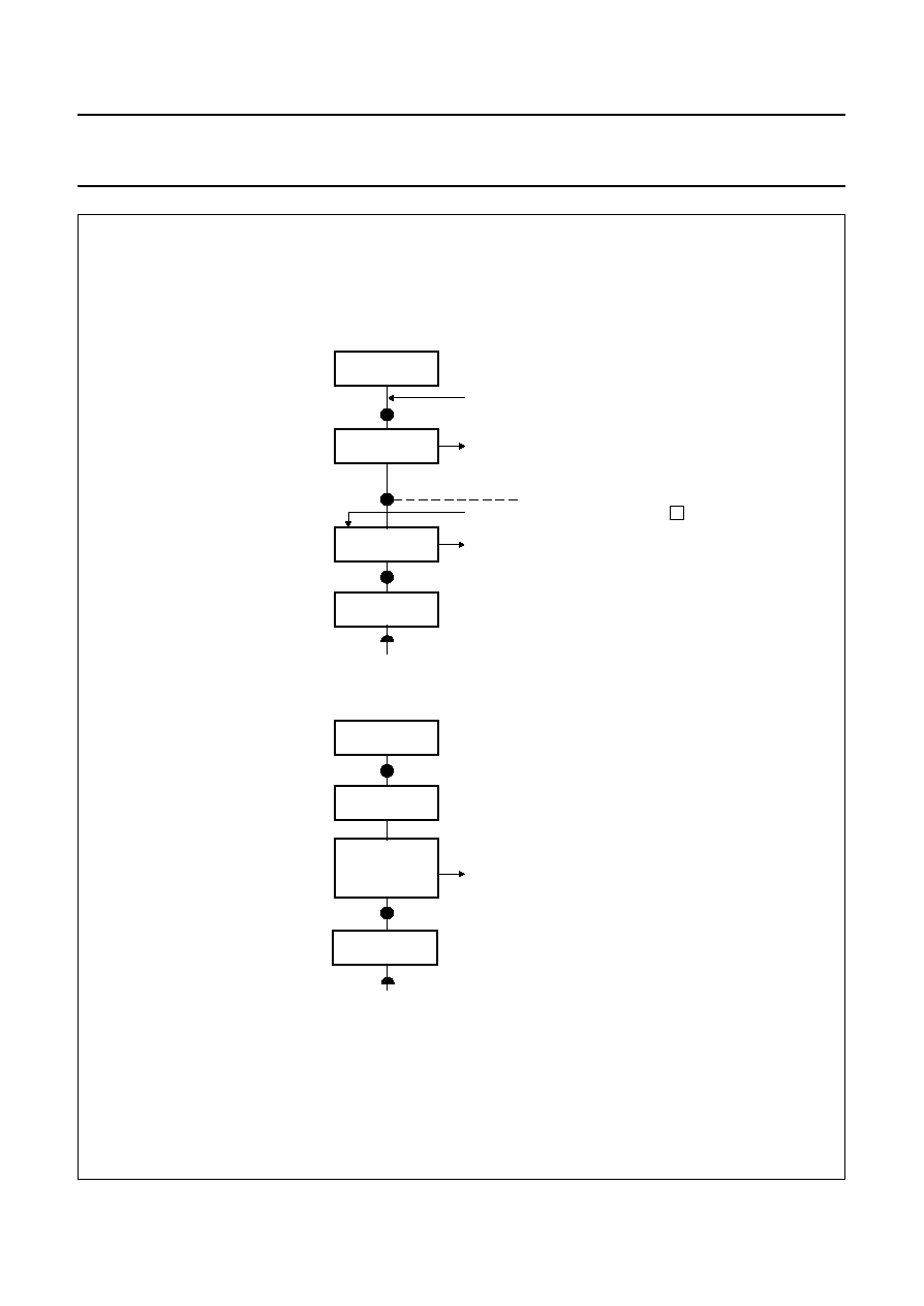
DIALLING PROCEDURES (see Figs 7, 8 and 9)
8.1
Dialling
After CE has risen to V
DD
the oscillator starts running and
the Read Address Counter (RAC) is set to the first address
of both the main and temporary redial registers, ready to
redial any stored number (see Fig.6). By dialling the first
valid digit, the Temporary Write Address Counter (TWAC)
will be set to the first address of the temporary register,
and the decoded digit will be stored in the temporary
register at that address. The TWAC is then incremented to
the next address. The first 5 valid digits will be decoded
and stored in the temporary register in this way, and have
no effect on the main register and its associated Write
Address Counter (WAC). After the sixth valid digit is
entered, the TWAC indicates an overflow condition.
The data from the temporary register will be copied into the
5 least significant places of the main register and the
TWAC into the WAC. The sixth digit, and all subsequent
digits will be stored in the main register (a total of not more
than 23). If more than 23 digits are entered redial will be
inhibited. If not more than 5 digits are entered only the
temporary register and the associated TWAC are affected.
All entries are debounced on both the leading and trailing
edges for at least time period t
e
as shown in Figs 11, 12,
13 and 14.
Each entry is tested for validity before being stored in the
redial registers.
·
For DTMF dialling all dial keys are valid
·
For pulse dialling only numeric dial keys are valid.
Simultaneous to their acceptance and corresponding to
the selected mode (pulse, DTMF or mixed), the entries are
transmitted as pulse-trains or as DTMF frequencies in
accordance with PTT requirements. Non-numeric dial key
entries are neglected during pulse dialling; they are neither
stored nor transmitted.

1996 Nov 21
11
Philips Semiconductors
Product specification
Pulse and DTMF diallers with redial
PCD3310; PCD3310A
8.2
Redialling
After CE has risen to V
DD
the oscillator starts running.
The address of the first digit in the redial register is stored
in the RAC, and the device is in the conversation mode.
If `R' is the first keyboard entry the device starts redialling
the contents of the temporary register. If the overflow flag
of the TWAC was set in the previous dialling, the redialling
continues in the main register.
Because access to an external line from a PABX usually
involves dialling an access code and waiting for an access
tone, a `one-press' redial may fail due to insufficient delay
between the access code and the external number.
For this reason, the access code should be redialled. If the
access code (up to 4 digits) matches the first part of the
stored number, then pressing R after the access tone is
obtained will cause the rest of the number to be redialled
(see Fig.7, PABX).
Timing in the DTMF mode is calibrated for both tone bursts
and pauses.
In mixed mode only the first part entered (the pulse dialled
part of the stored number) can be redialled.
During redial keyboard entries (function or non-function)
are not accepted until the device returns to the
conversation mode after completion of redialling. No redial
activity takes place if one of the following events occur:
·
Power-on reset
·
Memory clear (`P' without subsequent data entry)
·
Memory overflow (more than 23 valid data entries).
8.3
Notepad
The redial register can also be used as a notepad. In the
conversation mode a number with up to 23 digits can be
entered and stored for redialling. By activating the program
key (P) the WAC and TWAC pointers are reset. This acts
like a memory clear (redial is inhibited). Afterwards, by
entering and storing any digits, redialling will be possible
after flash or hook-on and hook-off (see Fig.9).
During notepad programming the numbers entered will not
be transmitted nor is the mute active, only the confidence
tone is generated.
handbook, full pagewidth
MGE493
5
4
3
2
1
addressed
through pointers
TWAC or RAC
TEMPORARY REGISTER
TEMPORARY WRITE
ADDRESS COUNTER (TWAC)
1
2
3
4
5
6
23
addressed
through pointers
WAC or RAC
MAIN REGISTER
write address counter (WAC)
read address counter (RAC)
ADDRESS COUNTER
Fig.6 Program memory map.

1996 Nov 21
12
Philips Semiconductors
Product specification
Pulse and DTMF diallers with redial
PCD3310; PCD3310A
handbook, full pagewidth
MGE494
external number
462 75 30
OFF-HOOK
OFF-HOOK
OFF-HOOK
OFF-HOOK
OFF-HOOK
OFF-HOOK
ON-HOOK
ON-HOOK
ON-HOOK
ON-HOOK
ON-HOOK
ON-HOOK
key-in R
key-in R
key-in R
462 75 30
internal number
12345
key-in
internal number
5 digits
12345
key-in
same previous
ACCESS DIGIT(S)
0
key-in
ACCESS DIGIT(S)
0
4 digits
key-in
external number
462 75 30
key-in
23 digits
462 75 30
REDIAL external number (1)
DIAL internal number
if internal number
5 digits
conversation
mode
standby
mode
pulse or
tone out
wait for
access tone
wait for
access tone
REDIAL internal number
REDIAL
PABX
DIAL external number
DIAL
PUBLIC EXCHANGE
Fig.7 Pulse or DTMF dialling mode.
(1) If [access digit(s) + external number]
23 digits.
1996 Nov 21
13
Philips Semiconductors
Product specification
Pulse and DTMF diallers with redial
PCD3310; PCD3310A
Fig.8 Pulse/DTMF and mixed mode dialling.
handbook, full pagewidth
MGE495
key-in
462 75 30
*
1 2 3 4 5 6 7
8 9 A B C D
#
OFF-HOOK
ON-HOOK
ON-HOOK
key-in R
462 75 30
if total
(PD
+
DTMF)
23 digits
OFF-HOOK
DIAL
set in pulse dialling
pulse output
wait for signal
(or any voice indication)
automatic switch to DTMF or manual by
TONE-output
pulse dialling
DTMF dialling
REDIAL
pulse dialling
pulse output
>
1996 Nov 21
14
Philips Semiconductors
Product specification
Pulse and DTMF diallers with redial
PCD3310; PCD3310A
Fig.9 Notepad, memory clear, flash; independent of dialling mode.
handbook, full pagewidth
MGE496
key-in
462 75 30
OFF-HOOK
OFF-HOOK
OFF-HOOK
OFF-HOOK
ON-HOOK
ON-HOOK
ON-HOOK
key-in FL
key-in R
key-in P
355 44 99
key-in R
key-in P
key-in
462 75 30
key-in
ACCESS DIGIT(S)
0
key-in
external number
462 75 30
key-in
internal number
12345
key-in
355 44 99
23 digits
OFF-HOOK
NOTEPAD REDIAL
NOTEPAD PROGRAM
no dialling - no muting
no
redialling
MEMORY CLEAR
wait for
access tone
wait for
access tone
REDIAL
(see PABX
procedure)
FLASH
1996 Nov 21
15
Philips Semiconductors
Product specification
Pulse and DTMF diallers with redial
PCD3310; PCD3310A
9
HANDLING
Inputs and outputs are protected against electrostatic discharge in normal handling. However, it is good practice to take
normal precautions appropriate to handling MOS devices (see
"Data Handbook ICO3, Section: General, Handling MOS
devices").
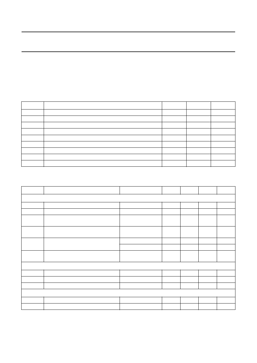
10 LIMITING VALUES
In accordance with the Absolute Maximum Rating System (IEC 134).
11 CHARACTERISTICS
V
DD
= 3 V; V
SS
= 0 V; f
osc
= 3.579545 MHz; T
amb
=
-
25 to +70
°
C; unless otherwise specified.
SYMBOL
PARAMETER
MIN.
MAX.
UNIT
V
DD
supply voltage
-
0.8
+8.0
V
I
DD
supply current
-
50
mA
I
I
DC input current
-
10
+
10
mA
I
O
DC output current
-
10
+
10
mA
V
I
all input voltages
-
0.8
V
DD
+ 0.8
V
P
tot
total power dissipation
-
300
mW
P
o
power dissipation per output
-
50
mW
T
stg
storage temperature range
-
65
+150
°
C
T
amb
operating ambient temperature
-
25
+70
°
C
SYMBOL
PARAMETER
CONDITIONS
MIN.
TYP.
MAX.
UNIT
Supply
V
DD
operating supply voltage
2.5
-
6.0
V
V
stb
standby supply voltage
1.8
-
6.0
V
I
DD(conv)
operating supply current in conversation
mode
oscillator ON
-
-
150
µ
A
I
DD(pulse)
operating supply current in pulse dialling
or flash mode
-
-
200
µ
A
I
DD(DTMF)
operating supply current in DTMF
dialling mode
tone ON
-
0.6
0.9
mA
one OFF
-
-
200
µ
A
I
DD(stb)
standby supply current
V
DD
= 1.8 V
oscillator OFF; note 1
-
1.4
4.0
µ
A
Inputs
V
IL
LOW level input voltage
0
-
0.3V
DD
V
V
IH
HIGH level input voltage
0.7V
DD
-
V
DD
V
I
LI
input leakage current pin CE
-
1
-
+1
µ
A
Keyboard inputs
R
KON
keyboard ON resistance
-
-
2
k
R
KOFF
keyboard OFF resistance
1
-
-
M

1996 Nov 21
16
Philips Semiconductors
Product specification
Pulse and DTMF diallers with redial
PCD3310; PCD3310A
Notes
1. Crystal connected between OSCI and OSCO; CE at V
SS
and all other pins open-circuit.
2. <
10 mA
dynamic current to set/reset PD/DTMF pin (mixed mode).
3. Flash inactive; output voltage = V
SS
.
4. Related to the level of the LOW group frequency component, according to CEPT recommendations.
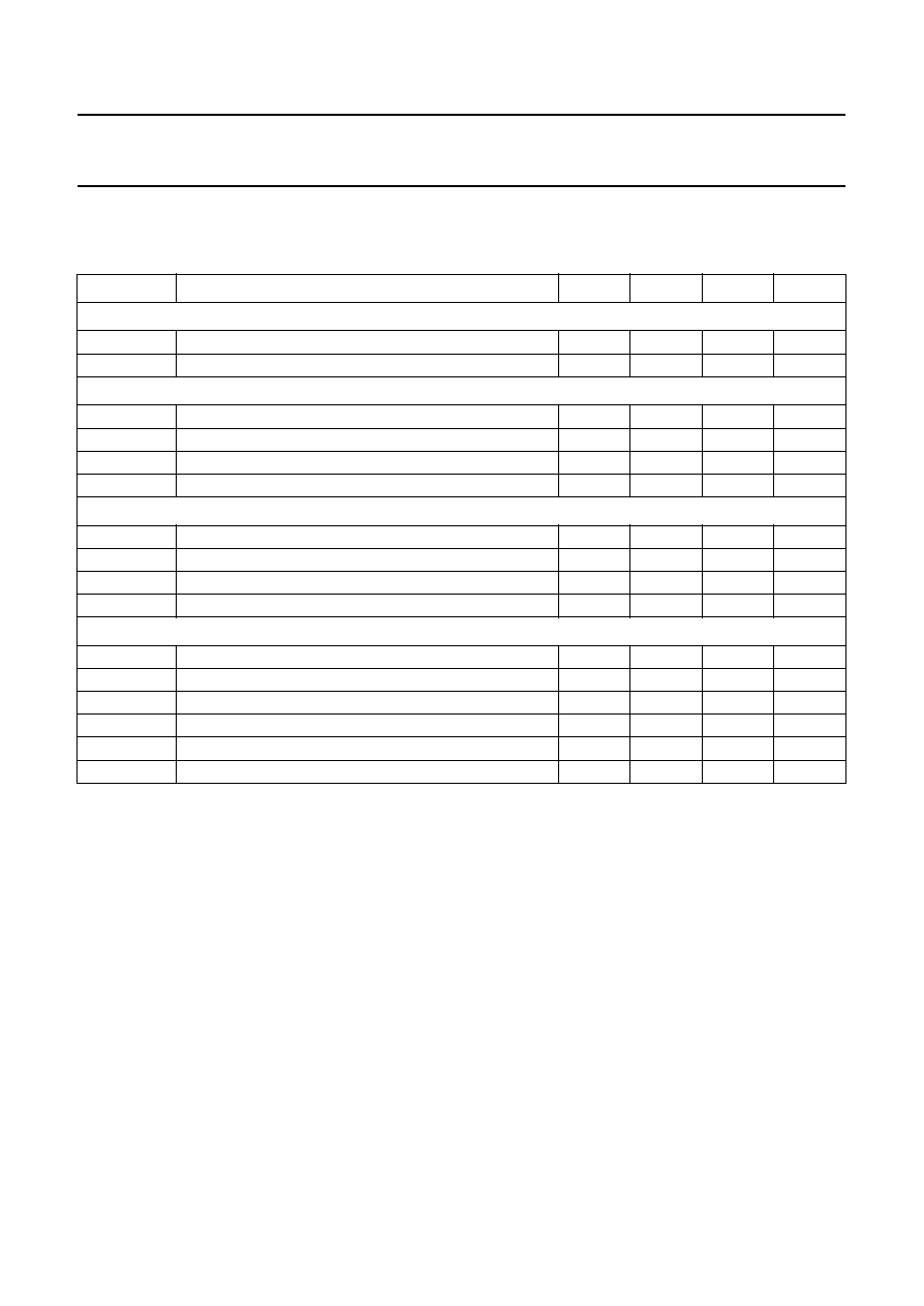
Outputs
I
OL
LOW level output sink current pins M1,
M1, DP/FLO, CF and FLD
V
OL
= V
SS
+ 0.5 V
0.7
-
-
mA
LOW level output sink current pin
PD/DTMF
V
OL
= V
SS
+ 0.5 V;
note 2
-
-
1
mA
I
OH
HIGH level output source current pins
M1, M1, DP/FLO, CF and M2
V
OH
= V
DD
-
0.5 V
-
0.6
-
-
mA
HIGH level output source current pin
PD/DTMF
V
OH
= V
DD
-
0.5 V;
note 2
-
-
-
1
mA
HIGH level output source current pin
FLD
V
OH
= V
DD
-
0.5 V;
note 3
-
-
60
-
nA
Tone output (see Fig.10)
V
HG(RMS)
DTMF output voltage levels for HIGH
group (RMS value)
V
DD
= 2.5 to 6 V
158
192
205
mV
V
LG(RMS)
DTMF output voltage levels for LOW
group (RMS value)
V
DD
= 2.5 to 6 V
125
150
160
mV
f
frequency deviation
-
0.6
-
+0.6
%
V
DC
DC voltage level
-
0.5V
DD
-
V
Z
O
output impedance
-
0.1
0.5
k
G
v
voltage gain (pre-emphasis) of group
1.85
2.1
2.35
dB
THD
total harmonic distortion
T
amb
= 25
°
C; note 4
-
-
25
-
dB
SYMBOL
PARAMETER
CONDITIONS
MIN.
TYP.
MAX.
UNIT
Fig.10 Tone output test circuit.
handbook, halfpage
VDD
VSS
PCD3310X
TONE
1
µ
F
50 pF
10 k
MGE501
1996 Nov 21
17
Philips Semiconductors
Product specification
Pulse and DTMF diallers with redial
PCD3310; PCD3310A
12 TIMING CHARACTERISTICS
When any key is activated a square wave (330 Hz) is generated and appears at the CF output to serve as an acoustic
feed-back for the user.
SYMBOL
PARAMETER
MIN.
TYP.
MAX.
UNIT
DTMF dialling
t
t
, t
p
transmission and pause times (manual dialling)
68
-
-
ms
t
t
, t
p
transmission and pause times (redialling)
68
70
72
ms
Pulse dialling (PCD3310)
f
dp
dialling pulse frequency
9.8
10
10.4
Hz
t
id
inter-digit pause
828
840
844
ms
t
b
break time
66
67
68
ms
t
m
make time
32
33
34
ms
Pulse dialling (PCD3310A)
f
dp
dialling pulse frequency
9.8
10
10.4
Hz
t
id
inter-digit pause
828
840
844
ms
t
b
break time
59
60
61
ms
t
m
make time
39
40
41
ms
General
t
FL
flash pulse duration
98
100
102
ms
t
flh
flash hold-over time
31
33
34
ms
t
h
hold-over time (muting on M1)
78
80
81
ms
t
on
clock start-up time
-
4
-
ms
t
e
debounce time
-
12
-
ms
t
rd
reset delay time
-
160
-
ms
1996 Nov 21
18
Philips Semiconductors
Product specification
Pulse and DTMF diallers with redial
PCD3310; PCD3310A
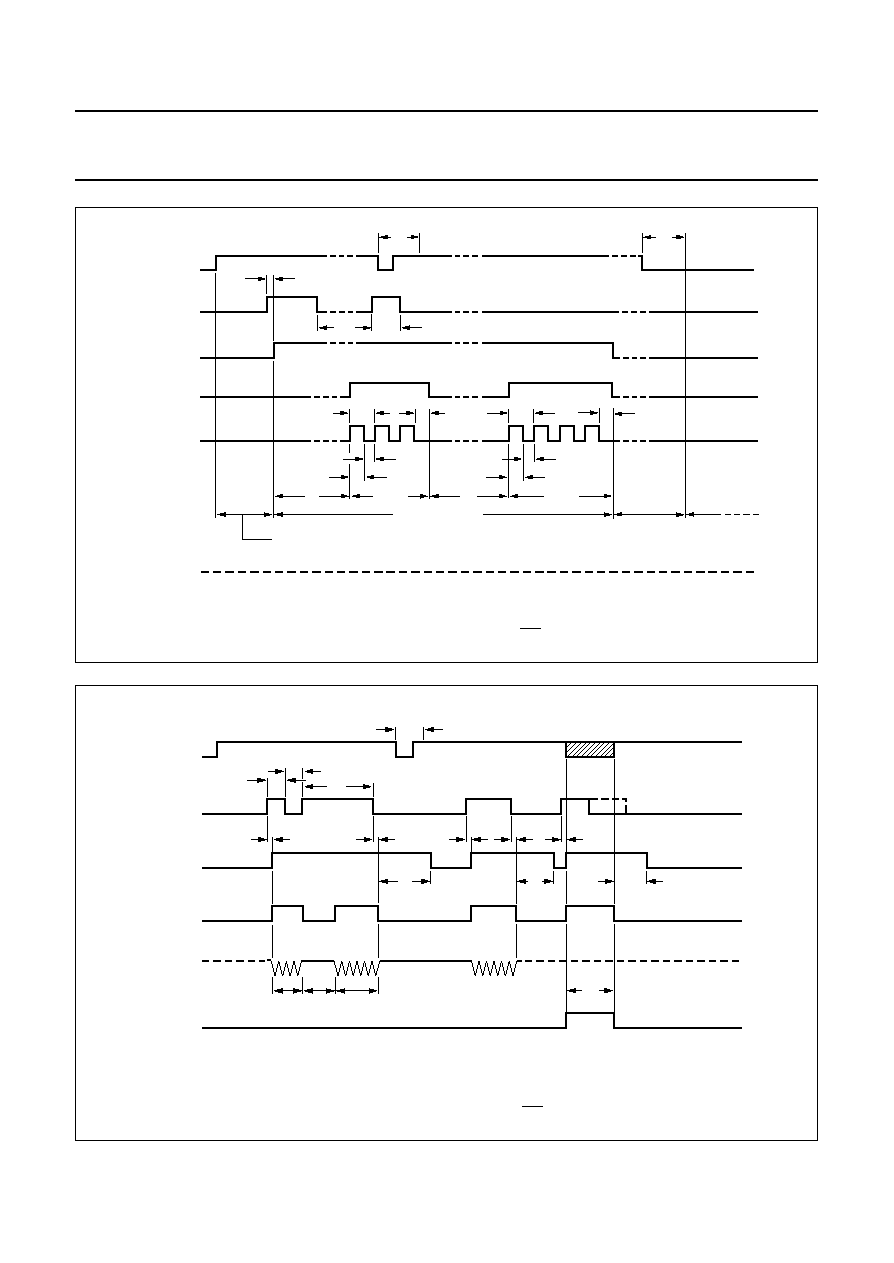
Fig.11 Timing diagram for pulse dialling (PD/DTMF = V
SS
).
handbook, full pagewidth
MGE497
trd
trd
(no effect)
te
>
te
>
te
T
T
tm
tm
tm
tm
tb
tb
tid
tid
n
×
tdp
n
×
tdp
DIALLING MODE
CONVERSATION
MODE
(await dialling tone)
CONVERSATION
MODE
STATIC
STANDBY
MODE
CE
KEYBOARD
ENTRY
M1
M2
DTMF
DP/FLO
3
4
1
2
3
1
2
3
4
The dashed line signifies floating.
Fig.12 Timing diagram for DTMF dialling (PD/DTMF = V
DD
).
handbook, full pagewidth
MGE498
1
2
(no effect)
3
F
CE
KEYBOARD
ENTRY
M1
M2
DTMF
DP/FLO
trd
<
tp
<
tt
>
tt
te
te
te
te
te
th
th
tflh
tfl
tt
tp
>
tt
The dashed line signifies floating.
1996 Nov 21
19
Philips Semiconductors
Product specification
Pulse and DTMF diallers with redial
PCD3310; PCD3310A
Fig.13 Timing diagram showing REDIAL where PABX access digits are the first keyboard entries in DTMF dialling
mode.
handbook, full pagewidth
MGE500
0
0
CE
KEYBOARD
ENTRY
M1
DTMF
R
telephone number
DIAL TONE
te
te
th
te
te
The dashed line signifies floating.
Fig.14 .Timing diagram for mixed mode (PD/DTMF open-circuit).
handbook, full pagewidth
MGE502
KEYBOARD
ENTRY
DTMF dialling
pulse dialling
DP/FLO
DTMF
M1
M2
PD/DTMF
2
2
te
te
te
te
te
tid
th
The dashed line signifies floating.
1996 Nov 21
20
Philips Semiconductors
Product specification
Pulse and DTMF diallers with redial
PCD3310; PCD3310A
13 APPLICATION INFORMATION
ook, full pagewidth
MGE503
123
45
6
78
9
0
#
P
FL
R
A
B
C
D
>
10
nF
to V
CC
BZX79/C12
R7
68
k
R8
390
100 pF
R2
130
k
R3
3.92
k
R11
130
R12
820
1%
1%
1%
C12
220
nF
R9
20
1%
R6
110
k
1%
4.7
µ
F
(10 V)
100
µ
F
(10 V)
2.2
nF
470
k
470
k
470
k
100 nF
R14
(2)
BST76
3.9
BC547
BZX79/C10
470 k
470 k
10 M
C14
2.2
µ
F
10 V
10 nF
R5
3.6
k
R4
100
k
C4
C7
10 pF
1 nF
10 nF
C13
2.2
µ
F
10
µ
F
10 V
redial
capacitor
BAV10
BAS11
10 k
150 nF
TONE
CE
V
DD
DP/
FLO
V
SS
M1
18
3
16
4
17
2
19
20
1
ROW 1
COL 4
COL 3
COL 2
ROW 2
ROW 3
ROW 4
ROW 5
COL 1
14
13
12
11
10
9
8
7
6
PD/DTMF
select pin
R13
to V
SS
(4)
(3)
-
U
4
×
BAS11
a/b
b/a
line
Z
l
450
Z
l
450
32
1
8
1
4
5
17
16
67
15
8
14
11
10
9
12
13
2.2 nF
C5
100
nF
BC557
BC547
BF423
to V
CC
Z
bal
TEA1060/61
PCD3310P
J2
(1)
R1
620
1%
1%
S1
1%
SLPE
AGC
V
CC
DTMF
Fig.15 Application diagram of the full electronic basic telephone set.
(1)
Automatic line compensation obtained by connecting R6 to V
SS
.
(2)
The value of resistor R14 is determined by the required level at LN and the DTMF gain of the TEA1060 and TEA1061.
(3)
Symmetrical low-impedance inputs for dynamic and magnetic microphones (TEA1060).
(4)
Asymmetrical high-impedance inputs for electret microphones (TEA1061).
1996 Nov 21
21
Philips Semiconductors
Product specification
Pulse and DTMF diallers with redial
PCD3310; PCD3310A
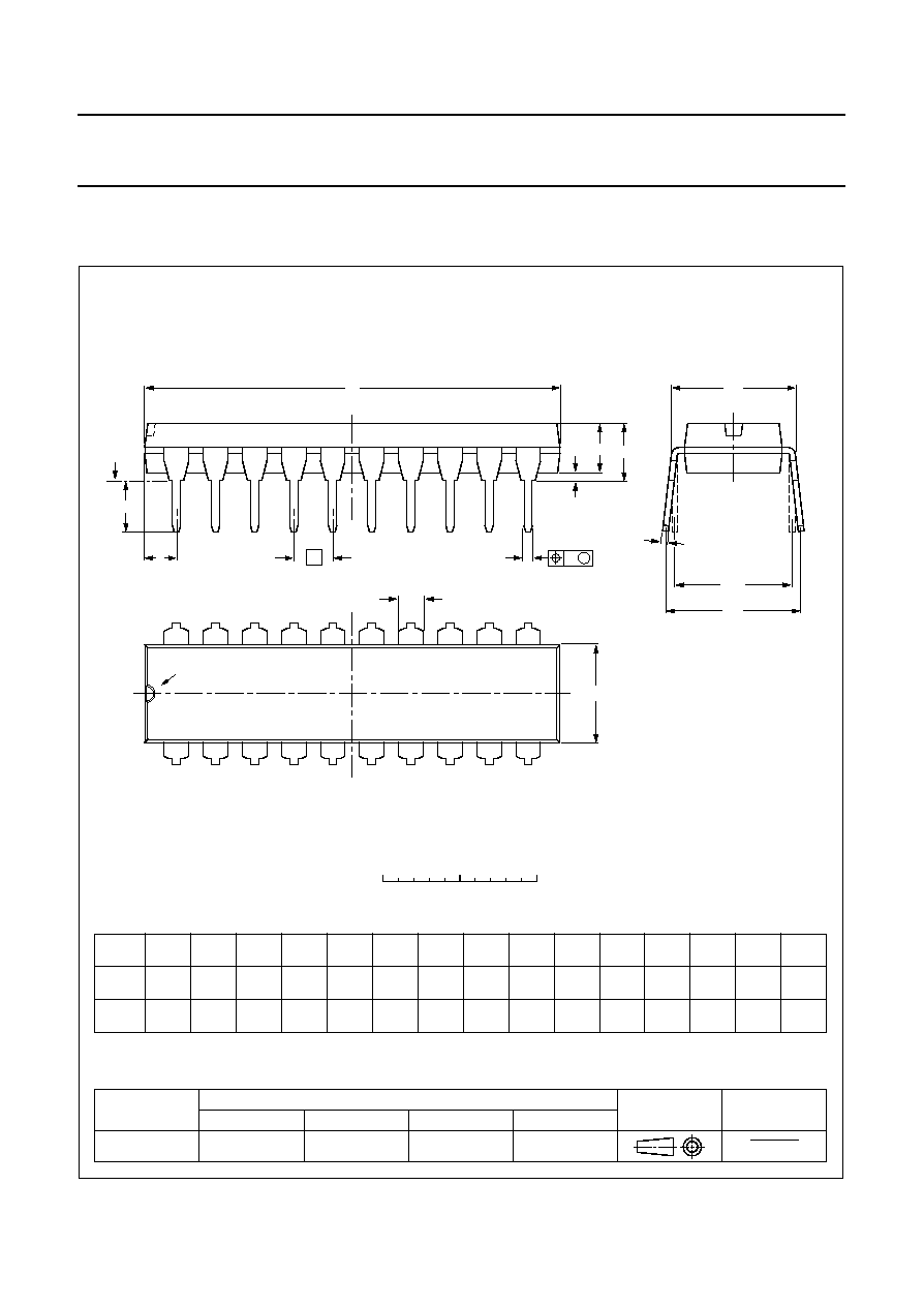
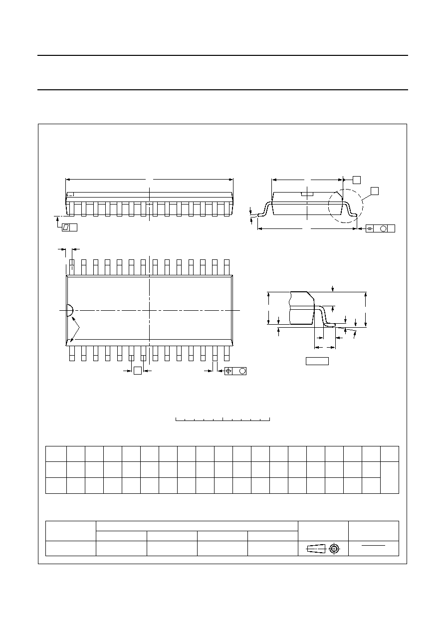
14 PACKAGE OUTLINES
UNIT
A
max.
1
2
b
1
c
D
E
e
M
H
L
REFERENCES
OUTLINE
VERSION
EUROPEAN
PROJECTION
ISSUE DATE
IEC
JEDEC
EIAJ
mm
inches
DIMENSIONS (inch dimensions are derived from the original mm dimensions)
SOT146-1
92-11-17
95-05-24
A
min.
A
max.
b
Z
max.
w
M
E
e
1
1.73
1.30
0.53
0.38
0.36
0.23
26.92
26.54
6.40
6.22
3.60
3.05
0.254
2.54
7.62
8.25
7.80
10.0
8.3
2.0
4.2
0.51
3.2
0.068
0.051
0.021
0.015
0.014
0.009
1.060
1.045
0.25
0.24
0.14
0.12
0.01
0.10
0.30
0.32
0.31
0.39
0.33
0.078
0.17
0.020
0.13
SC603
M
H
c
(e )
1
M
E
A
L
seating plane
A
1
w
M
b
1
e
D
A
2
Z
20
1
11
10
b
E
pin 1 index
0
5
10 mm
scale
Note
1. Plastic or metal protrusions of 0.25 mm maximum per side are not included.
(1)
(1)
(1)
DIP20: plastic dual in-line package; 20 leads (300 mil)
SOT146-1
1996 Nov 21
22
Philips Semiconductors
Product specification
Pulse and DTMF diallers with redial
PCD3310; PCD3310A
UNIT
A
max.
A
1
A
2
A
3
b
p
c
D
(1)
E
(1)
(1)
e
H
E
L
L
p
Q
Z
y
w
v
REFERENCES
OUTLINE
VERSION
EUROPEAN
PROJECTION
ISSUE DATE
IEC
JEDEC
EIAJ
mm
inches
2.65
0.30
0.10
2.45
2.25
0.49
0.36
0.32
0.23
18.1
17.7
7.6
7.4
1.27
10.65
10.00
1.1
1.0
0.9
0.4
8
0
o
o
0.25
0.1
DIMENSIONS (inch dimensions are derived from the original mm dimensions)
Note
1. Plastic or metal protrusions of 0.15 mm maximum per side are not included.
1.1
0.4
SOT136-1
91-08-13
95-01-24
X
14
28
w
M
A
A
1
A
2
b
p
D
H
E
L
p
Q
detail X
E
Z
c
L
v
M
A
e
15
1
(A )
3
A
y
0.25
075E06
MS-013AE
pin 1 index
0.10
0.012
0.004
0.096
0.089
0.019
0.014
0.013
0.009
0.71
0.69
0.30
0.29
0.050
1.4
0.055
0.42
0.39
0.043
0.039
0.035
0.016
0.01
0.25
0.01
0.004
0.043
0.016
0.01
0
5
10 mm
scale
SO28: plastic small outline package; 28 leads; body width 7.5 mm
SOT136-1

1996 Nov 21
23
Philips Semiconductors
Product specification
Pulse and DTMF diallers with redial
PCD3310; PCD3310A
15 SOLDERING
15.1
Introduction
There is no soldering method that is ideal for all IC
packages. Wave soldering is often preferred when
through-hole and surface mounted components are mixed
on one printed-circuit board. However, wave soldering is
not always suitable for surface mounted ICs, or for
printed-circuits with high population densities. In these
situations reflow soldering is often used.
This text gives a very brief insight to a complex technology.
A more in-depth account of soldering ICs can be found in
our
"IC Package Databook" (order code 9398 652 90011).
15.2
DIP
15.2.1
S
OLDERING BY DIPPING OR BY WAVE
The maximum permissible temperature of the solder is
260
°
C; solder at this temperature must not be in contact
with the joint for more than 5 seconds. The total contact
time of successive solder waves must not exceed
5 seconds.
The device may be mounted up to the seating plane, but
the temperature of the plastic body must not exceed the
specified maximum storage temperature (T
stg max
). If the
printed-circuit board has been pre-heated, forced cooling
may be necessary immediately after soldering to keep the
temperature within the permissible limit.
15.2.2
R
EPAIRING SOLDERED JOINTS
Apply a low voltage soldering iron (less than 24 V) to the
lead(s) of the package, below the seating plane or not
more than 2 mm above it. If the temperature of the
soldering iron bit is less than 300
°
C it may remain in
contact for up to 10 seconds. If the bit temperature is
between 300 and 400
°
C, contact may be up to 5 seconds.
15.3
SO
15.3.1
R
EFLOW SOLDERING
Reflow soldering techniques are suitable for all SO
packages.
Reflow soldering requires solder paste (a suspension of
fine solder particles, flux and binding agent) to be applied
to the printed-circuit board by screen printing, stencilling or
pressure-syringe dispensing before package placement.
Several techniques exist for reflowing; for example,
thermal conduction by heated belt. Dwell times vary
between 50 and 300 seconds depending on heating
method. Typical reflow temperatures range from
215 to 250
°
C.
Preheating is necessary to dry the paste and evaporate
the binding agent. Preheating duration: 45 minutes at
45
°
C.
15.3.2
W
AVE SOLDERING
Wave soldering techniques can be used for all SO
packages if the following conditions are observed:
·
A double-wave (a turbulent wave with high upward
pressure followed by a smooth laminar wave) soldering
technique should be used.
·
The longitudinal axis of the package footprint must be
parallel to the solder flow.
·
The package footprint must incorporate solder thieves at
the downstream end.
During placement and before soldering, the package must
be fixed with a droplet of adhesive. The adhesive can be
applied by screen printing, pin transfer or syringe
dispensing. The package can be soldered after the
adhesive is cured.
Maximum permissible solder temperature is 260
°
C, and
maximum duration of package immersion in solder is
10 seconds, if cooled to less than 150
°
C within
6 seconds. Typical dwell time is 4 seconds at 250
°
C.
A mildly-activated flux will eliminate the need for removal
of corrosive residues in most applications.
15.3.3
R
EPAIRING SOLDERED JOINTS
Fix the component by first soldering two diagonally-
opposite end leads. Use only a low voltage soldering iron
(less than 24 V) applied to the flat part of the lead. Contact
time must be limited to 10 seconds at up to 300
°
C. When
using a dedicated tool, all other leads can be soldered in
one operation within 2 to 5 seconds between
270 and 320
°
C.

1996 Nov 21
24
Philips Semiconductors
Product specification
Pulse and DTMF diallers with redial
PCD3310; PCD3310A
16 DEFINITIONS
Data sheet status
Objective specification
This data sheet contains target or goal specifications for product development.
Preliminary specification
This data sheet contains preliminary data; supplementary data may be published later.
Product specification
This data sheet contains final product specifications.
Limiting values
Limiting values given are in accordance with the Absolute Maximum Rating System (IEC 134). Stress above one or
more of the limiting values may cause permanent damage to the device. These are stress ratings only and operation
of the device at these or at any other conditions above those given in the Characteristics sections of the specification
is not implied. Exposure to limiting values for extended periods may affect device reliability.
Application information
Where application information is given, it is advisory and does not form part of the specification.

1996 Nov 21
25
Philips Semiconductors
Product specification
Pulse and DTMF diallers with redial
PCD3310; PCD3310A
NOTES

1996 Nov 21
26
Philips Semiconductors
Product specification
Pulse and DTMF diallers with redial
PCD3310; PCD3310A
NOTES

1996 Nov 21
27
Philips Semiconductors
Product specification
Pulse and DTMF diallers with redial
PCD3310; PCD3310A
NOTES

Internet: http://www.semiconductors.philips.com
Philips Semiconductors a worldwide company
© Philips Electronics N.V. 1996
SCA52
All rights are reserved. Reproduction in whole or in part is prohibited without the prior written consent of the copyright owner.
The information presented in this document does not form part of any quotation or contract, is believed to be accurate and reliable and may be changed
without notice. No liability will be accepted by the publisher for any consequence of its use. Publication thereof does not convey nor imply any license
under patent- or other industrial or intellectual property rights.
Netherlands: Postbus 90050, 5600 PB EINDHOVEN, Bldg. VB,
Tel. +31 40 27 82785, Fax. +31 40 27 88399
New Zealand: 2 Wagener Place, C.P.O. Box 1041, AUCKLAND,
Tel. +64 9 849 4160, Fax. +64 9 849 7811
Norway: Box 1, Manglerud 0612, OSLO,
Tel. +47 22 74 8000, Fax. +47 22 74 8341
Philippines: Philips Semiconductors Philippines Inc.,
106 Valero St. Salcedo Village, P.O. Box 2108 MCC, MAKATI,
Metro MANILA, Tel. +63 2 816 6380, Fax. +63 2 817 3474
Poland: Ul. Lukiska 10, PL 04-123 WARSZAWA,
Tel. +48 22 612 2831, Fax. +48 22 612 2327
Portugal: see Spain
Romania: see Italy
Russia: Philips Russia, Ul. Usatcheva 35A, 119048 MOSCOW,
Tel. +7 095 247 9145, Fax. +7 095 247 9144
Singapore: Lorong 1, Toa Payoh, SINGAPORE 1231,
Tel. +65 350 2538, Fax. +65 251 6500
Slovakia: see Austria
Slovenia: see Italy
South Africa: S.A. PHILIPS Pty Ltd., 195-215 Main Road Martindale,
2092 JOHANNESBURG, P.O. Box 7430 Johannesburg 2000,
Tel. +27 11 470 5911, Fax. +27 11 470 5494
South America: Rua do Rocio 220, 5th floor, Suite 51,
04552-903 Săo Paulo, SĂO PAULO - SP, Brazil,
Tel. +55 11 821 2333, Fax. +55 11 829 1849
Spain: Balmes 22, 08007 BARCELONA,
Tel. +34 3 301 6312, Fax. +34 3 301 4107
Sweden: Kottbygatan 7, Akalla, S-16485 STOCKHOLM,
Tel. +46 8 632 2000, Fax. +46 8 632 2745
Switzerland: Allmendstrasse 140, CH-8027 ZÜRICH,
Tel. +41 1 488 2686, Fax. +41 1 481 7730
Taiwan: PHILIPS TAIWAN Ltd., 23-30F, 66,
Chung Hsiao West Road, Sec. 1, P.O. Box 22978,
TAIPEI 100, Tel. +886 2 382 4443, Fax. +886 2 382 4444
Thailand: PHILIPS ELECTRONICS (THAILAND) Ltd.,
209/2 Sanpavuth-Bangna Road Prakanong, BANGKOK 10260,
Tel. +66 2 745 4090, Fax. +66 2 398 0793
Turkey: Talatpasa Cad. No. 5, 80640 GÜLTEPE/ISTANBUL,
Tel. +90 212 279 2770, Fax. +90 212 282 6707
Ukraine: PHILIPS UKRAINE, 4 Patrice Lumumba str., Building B, Floor 7,
252042 KIEV, Tel. +380 44 264 2776, Fax. +380 44 268 0461
United Kingdom: Philips Semiconductors Ltd., 276 Bath Road, Hayes,
MIDDLESEX UB3 5BX, Tel. +44 181 730 5000, Fax. +44 181 754 8421
United States: 811 East Arques Avenue, SUNNYVALE, CA 94088-3409,
Tel. +1 800 234 7381
Uruguay: see South America
Vietnam: see Singapore
Yugoslavia: PHILIPS, Trg N. Pasica 5/v, 11000 BEOGRAD,
Tel. +381 11 625 344, Fax.+381 11 635 777
For all other countries apply to: Philips Semiconductors, Marketing & Sales Communications,
Building BE-p, P.O. Box 218, 5600 MD EINDHOVEN, The Netherlands, Fax. +31 40 27 24825
Argentina: see South America
Australia: 34 Waterloo Road, NORTH RYDE, NSW 2113,
Tel. +61 2 9805 4455, Fax. +61 2 9805 4466
Austria: Computerstr. 6, A-1101 WIEN, P.O. Box 213,
Tel. +43 1 60 101, Fax. +43 1 60 101 1210
Belarus: Hotel Minsk Business Center, Bld. 3, r. 1211, Volodarski Str. 6,
220050 MINSK, Tel. +375 172 200 733, Fax. +375 172 200 773
Belgium: see The Netherlands
Brazil: see South America
Bulgaria: Philips Bulgaria Ltd., Energoproject, 15th floor,
51 James Bourchier Blvd., 1407 SOFIA,
Tel. +359 2 689 211, Fax. +359 2 689 102
Canada: PHILIPS SEMICONDUCTORS/COMPONENTS,
Tel. +1 800 234 7381
China/Hong Kong: 501 Hong Kong Industrial Technology Centre,
72 Tat Chee Avenue, Kowloon Tong, HONG KONG,
Tel. +852 2319 7888, Fax. +852 2319 7700
Colombia: see South America
Czech Republic: see Austria
Denmark: Prags Boulevard 80, PB 1919, DK-2300 COPENHAGEN S,
Tel. +45 32 88 2636, Fax. +45 31 57 1949
Finland: Sinikalliontie 3, FIN-02630 ESPOO,
Tel. +358 9 615800, Fax. +358 9 61580/xxx
France: 4 Rue du Port-aux-Vins, BP317, 92156 SURESNES Cedex,
Tel. +33 1 40 99 6161, Fax. +33 1 40 99 6427
Germany: Hammerbrookstraße 69, D-20097 HAMBURG,
Tel. +49 40 23 53 60, Fax. +49 40 23 536 300
Greece: No. 15, 25th March Street, GR 17778 TAVROS/ATHENS,
Tel. +30 1 4894 339/239, Fax. +30 1 4814 240
Hungary: see Austria
India: Philips INDIA Ltd, Shivsagar Estate, A Block, Dr. Annie Besant Rd.
Worli, MUMBAI 400 018, Tel. +91 22 4938 541, Fax. +91 22 4938 722
Indonesia: see Singapore
Ireland: Newstead, Clonskeagh, DUBLIN 14,
Tel. +353 1 7640 000, Fax. +353 1 7640 200
Israel: RAPAC Electronics, 7 Kehilat Saloniki St, TEL AVIV 61180,
Tel. +972 3 645 0444, Fax. +972 3 649 1007
Italy: PHILIPS SEMICONDUCTORS, Piazza IV Novembre 3,
20124 MILANO, Tel. +39 2 6752 2531, Fax. +39 2 6752 2557
Japan: Philips Bldg 13-37, Kohnan 2-chome, Minato-ku, TOKYO 108,
Tel. +81 3 3740 5130, Fax. +81 3 3740 5077
Korea: Philips House, 260-199 Itaewon-dong, Yongsan-ku, SEOUL,
Tel. +82 2 709 1412, Fax. +82 2 709 1415
Malaysia: No. 76 Jalan Universiti, 46200 PETALING JAYA, SELANGOR,
Tel. +60 3 750 5214, Fax. +60 3 757 4880
Mexico: 5900 Gateway East, Suite 200, EL PASO, TEXAS 79905,
Tel. +9-5 800 234 7381
Middle East: see Italy
Printed in The Netherlands
417021/1200/03/pp28
Date of release: 1996 Nov 21
Document order number:
9397 750 01075