Philips Semiconductors
Objective data sheet
PCA9536
4-bit I
2
C and SMBus I/O port
2
2004 Aug 20
FEATURES
·
4-bit I
2
C GPIO
·
Operating power supply voltage range of 2.3 to 5.5 V
·
5 V tolerant I/Os
·
Polarity inversion register
·
Active low interrupt output
·
Low stand-by current
·
Noise filter on SCL/SDA inputs
·
No glitch on power-up
·
Internal power-on reset
·
4 I/O pins which default to 4 inputs with 100 k
internal pull-up
resistor
·
0 to 400 kHz clock frequency
·
ESD protection exceeds 2000 V HBM per JESD22-A114,
200 V MM per JESD22-A115 and 1000 V CDM per JESD22-C101
·
Latch-up testing is done to JESDEC Standard JESD78 which
exceeds 100 mA
·
Two packages offered: SO8 and TSSOP8
DESCRIPTION
The PCA9536 is 8-pin CMOS devices that provides 4 bits of
General Purpose parallel Input/Output (GPIO) expansion for
I
2
C/SMBus applications and were developed to enhance the Philips
family of I
@
C I/O expanders. I/O expanders provides a simple
solution when additional I/O is needed for ACPI power switches,
sensors, pushbuttons, LEDs, fans, etc.
The PCA9536 consists of a 4-bit Configuration register (Input or
Output selection); 4-bit Input register, 4-bit Output register and an
4-bit Polarity inversion register (Active-HIGH or Active-LOW
operation). The system master can enable the I/Os as either inputs
or outputs by writing to the I/O configuration bits. The data for each
Input or Output is kept in the corresponding Input or Output register.
The polarity of the read register can be inverted with the Polarity
Inversion Register. All registers can be read by the system master.
The power-on reset sets the registers to their default values and
initializes the device state machine.
The I
2
C address is fixed and allows only one device on the same
I
2
C/SMBus.
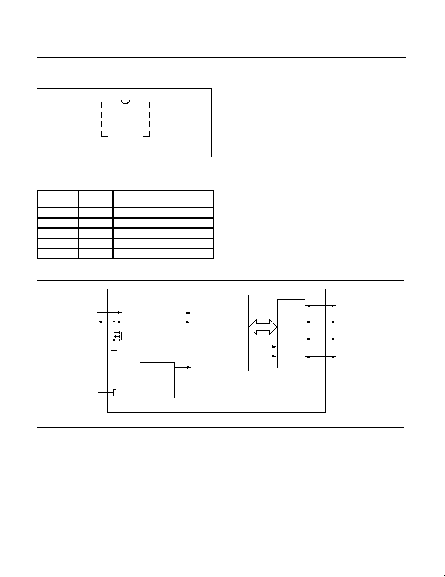
ORDERING INFORMATION
PACKAGES
TEMPERATURE
RANGE
ORDER CODE
TOPSIDE MARK
DRAWING NUMBER
8-Pin Plastic SO (wide)
40
°
C to +85
°
C
PCA9536D
PCA9536
SOT96-1
8-Pin Plastic TSSOP
40
°
C to +85
°
C
PCA9536DP
9536
SOT505-1
Standard packing quantities and other packaging data are available at www.philipslogic.com/packaging.
I
2
C is a trademark of Philips Semiconductors Corporation.
SMBus as specified by the Smart Battery System Implementers Forum is a derivative of the Philips I
2
C patent.

Philips Semiconductors
Objective data sheet
PCA9536
4-bit I
2
C and SMBus I/O port
2004 Aug 20
4
REGISTERS
Command Byte
Command
Protocol
Function
0
Read byte
Input port register
1
Read/write byte
Output port register
2
Read/write byte
Polarity inversion register
3
Read/write byte
Configuration register
The command byte is the first byte to follow the address byte during
a write transmission. It is used as a pointer to determine which of the
following registers will be written or read.
Register 0 Input Port Register
bit
X
X
X
X
I3
I2
I1
I0
default
1
1
1
1
1
1
1
1
This register is a read only port. It reflects the incoming logic levels
of the pins, regardless of whether the pin is defined as an input or an
output by Register 3. Writes to this register have no effect.
"X" are "don't care" bits and can be programmed with either "0"
or "1".
Register 1 Output Port Register
bit
X
X
X
X
O3
O2
O1
O0
default
1
1
1
1
1
1
1
1
This register reflects the outgoing logic levels of the pins defined as
outputs by Register 3. Bit values in this register have no effect on
pins defined as inputs. Reads from this register return the value that
is in the flip-flop controlling the output selection, NOT the actual pin
value.
"X" are "don't care" bits and can be programmed with either "0"
or "1".
Register 2 Polarity Inversion Register
bit
X
X
X
X
N3
N2
N1
N0
default
0
0
0
0
0
0
0
0
This register allows the user to invert the polarity of the Input Port
Register data. If a bit in this register is set (written with `1'), the
corresponding Input Port data is inverted. If a bit in this register is
cleared (written with a `0'), the Input Port data polarity is retained.
"X" are "don't care" bits and can be programmed with either "0"
or "1".
Register 3 Configuration Register
bit
X
X
X
X
C3
C2
C1
C0
default
1
1
1
1
1
1
1
1
This register configures the directions of the I/O pins. If a bit in this
register is set, the corresponding port pin is enabled as an input with
high impedance output driver. If a bit in this register is cleared, the
corresponding port pin is enabled as an output. At reset, the I/Os are
configured as inputs with a weak pull-up to V
DD
.
"X" are "don't care" bits and can be programmed with either "0"
or "1".
Power-on Reset
When power is applied to V
DD
, an internal power-on reset holds the
PCA9536 in a reset condition until V
DD
has reached V
POR
. At that
point, the reset condition is released and the PCA9536 registers and
state machine will initialize to their default states. Thereafter, V
DD
must be lowered below 0.2 V to reset the device.
For a power reset cycle, V
DD
must be lowered below 0.2 V and then
restored to the operating voltage.

Philips Semiconductors
Objective data sheet
PCA9536
4-bit I
2
C and SMBus I/O port
2004 Aug 20
5
SIMPLIFIED SCHEMATIC OF I/O0 TO I/O3
WRITE PULSE
DATA FROM
SHIFT REGISTER
V
DD
I/O0 TO I/O3
V
SS
WRITE
CONFIGURATION
PULSE
D
C
K
FF
Q
D
C
K
Q
FF
D
C
K
Q
FF
D
C
K
Q
FF
INPUT PORT
REGISTER
POLARITY
INVERSION
REGISTER
OUTPUT
PORT
REGISTER
DATA FROM
SHIFT REGISTER
DATA FROM
SHIFT REGISTER
WRITE
POLARITY
PULSE
CONFIGURATION
REGISTER
OUTPUT PORT
REGISTER DATA
INPUT PORT
REGISTER DATA
POLARITY
REGISTER DATA
READ PULSE
SW02192
Q
Q
Q
Q
100 k
Q1
Q2
ESD PROTECTION DIODE
ESD PROTECTION DIODE
NOTE:
At Power-on Reset, all registers return to default values.
Figure 3. Simplified schematic of I/O0 to I/O3
I/O port
When an I/O is configured as an input, FETs Q1 and Q2 are off, creating a high impedance input with a weak pull-up (100 k
typ.) to V
DD
. The
input voltage may be raised above V
DD
to a maximum of 5.5 V.
If the I/O is configured as an output, then either Q1 or Q2 is enabled, depending on the state of the output port register. Care should be
exercised if an external voltage is applied to an I/O configured as an output because of the low impedance paths that exist between the pin and
either V
DD
or V
SS
.