Document Outline
- DESCRIPTION
- FEATURES
- ORDERING INFORMATION
- PIN CONFIGURATION
- PIN DESCRIPTION
- FUNCTIONAL DESCRIPTION
- APPLICATION INFORMATION
- ABSOLUTE MAXIMUM RATINGS
- DC ELECTRICAL CHARACTERISTICS
- DC ELECTRICAL CHARACTERISTICS
- AC ELECTRICAL CHARACTERISTICS
- AC ELECTRICAL CHARACTERISTICS
- AC WAVEFORMS
- TEST CIRCUIT
- SO8: plastic small outline package; 8 leads; body width 3.9 mm SOT96-1
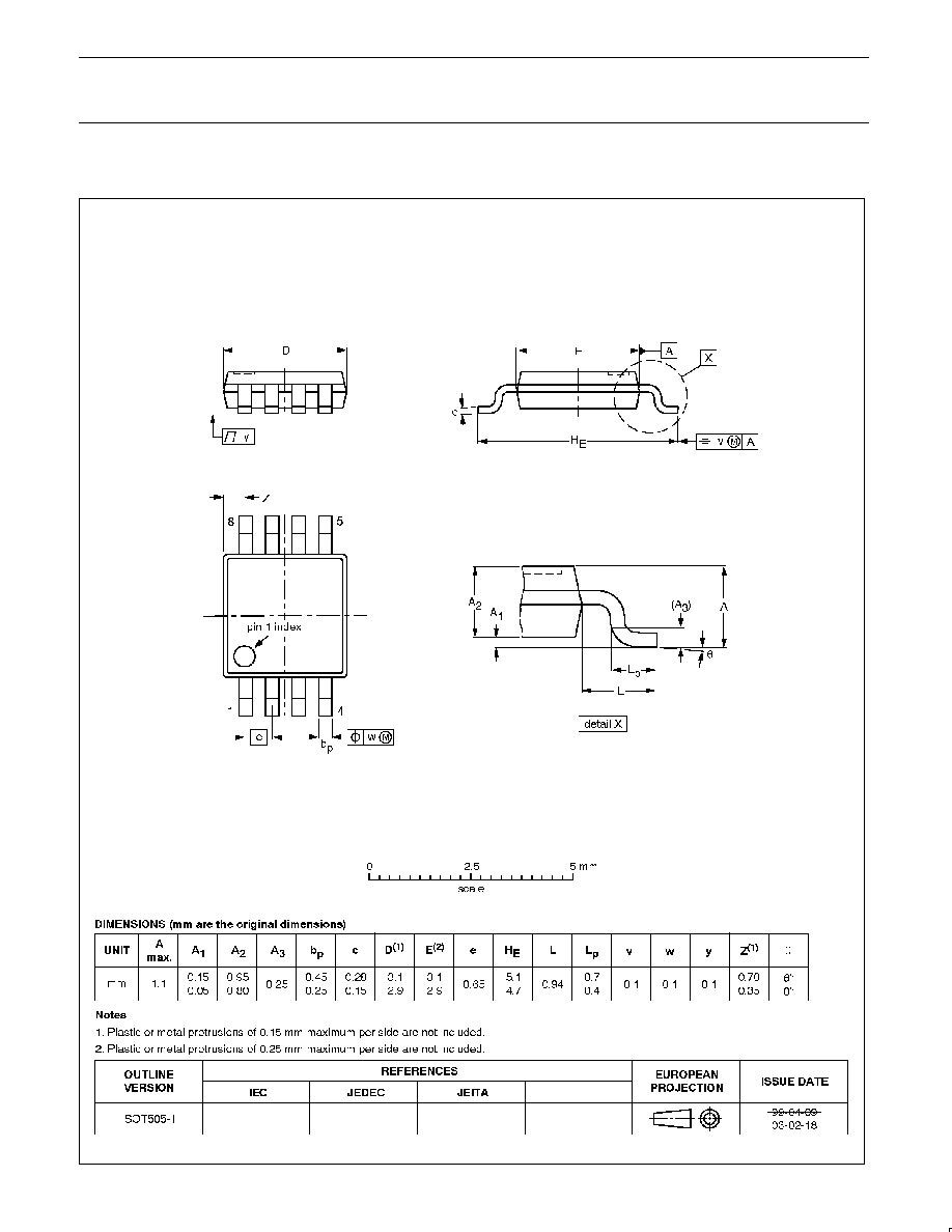
- TSSOP8: plastic thin shrink small outline package; 8 leads; body width 3 mm SOT505-1
- REVISION HISTORY
- Data sheet status
- Definitions
- Disclaimers
Philips
Semiconductors
PCA9515A
I
2
C-bus repeater
Product data sheet
Supersedes data of 2004 Jul 09
2004 Sep 29
INTEGRATED CIRCUITS
Philips Semiconductors
Product data sheet
PCA9515A
I
2
C-bus repeater
2
2004 Sep 29
DESCRIPTION
The PCA9515A is a CMOS integrated circuit intended for application
in I
2
C and SMBus systems.
While retaining all the operating modes and features of the I
2
C
system it permits extension of the I
2
C-bus by buffering both the data
(SDA) and the clock (SCL) lines, thus enabling two buses of 400 pF.
The I
2
C-bus capacitance limit of 400 pF restricts the number of
devices and bus length. Using the PCA9515A enables the system
designer to isolate two halves of a bus, thus more devices or longer
length can be accommodated. It can also be used to run two buses,
one at 5 V and the other at 3.3 V or a 400 kHz and 100 kHz bus,
where the 100 kHz bus is isolated when 400 kHz operation of the
other is required.
Two or more PCA9515As cannot be put in series. The PCA9515A
design does not allow this configuration. Since there is no direction
pin, slightly different "legal" low voltage levels are used to avoid
lock-up conditions between the input and the output. A "regular
LOW" applied at the input of a PCA9515A will be propagated as a
"buffered LOW" with a slightly higher value. When this "buffered
LOW" is applied to another PCA9515A, PCA9516A, or PCA9518 in
series, the second PCA9515A, PCA9516A, or PCA9518 will not
recognize it as a "regular LOW" and will not propagate it as a
"buffered LOW" again. The PCA9510/9511/9513/9514 and
PCA9512 cannot be used in series with the PCA9515A, PCA9516A,
or PCA9518 but can be used in series with themselves since they
use shifting instead of static offsets to avoid lock-up conditions.
FEATURES
·
2 channel, bi-directional buffer
·
I
2
C-bus and SMBus compatible
·
Active-HIGH repeater enable input
·
Open-drain input/outputs
·
Lock-up free operation
·
Supports arbitration and clock stretching across the repeater
·
Accommodates standard mode and fast mode I
2
C devices and
multiple masters
·
Powered-off high-impedance I
2
C pins
·
Operating supply voltage range of 2.3 V to 3.6 V
·
5.5 V tolerant I
2
C and enable pins
·
0 to 400 kHz clock frequency
1
·
ESD protection exceeds 2000 V HBM per JESD22-A114,
200 V MM per JESD22-A115, and 1000 V CDM per
JESD22-C101.
·
Latch-up testing is done to JEDEC Standard JESD78 which
exceeds 100 mA.
·
Package offerings: SO and TSSOP (MSOP)
PIN CONFIGURATION
1
2
3
4
n.c.
GND
SDA0
SCL1
SDA1
EN
5
6
7
8
V
CC
SCL0
SU01322
Figure 1. Pin configuration
PIN DESCRIPTION
PIN
SYMBOL
FUNCTION
1
n.c.
No connection
2
SCL0
Serial clock bus 0
3
SDA0
Serial data bus 0
4
GND
Supply ground
5
EN
Active-HIGH repeater enable input
6
SDA1
Serial data bus 1
7
SCL1
Serial clock bus 1
8
V
CC
Supply power
ORDERING INFORMATION
PACKAGES
TEMPERATURE RANGE
ORDER CODE
TOPSIDE MARK
DRAWING NUMBER
8-pin plastic SO
40
°
C to +85
°
C
PCA9515AD
PA9515A
SOT96-1
8-pin plastic TSSOP (MSOP)
40
°
C to +85
°
C
PCA9515ADP
9515A
SOT505-1
Standard packing quantities and other packaging data are available at www.standardproducts.philips.com/packaging.
1.
The maximum system operating frequency may be less than 400 kHz because of the delays added by the repeater.
Philips Semiconductors
Product data sheet
PCA9515A
I
2
C-bus repeater
2004 Sep 29
3
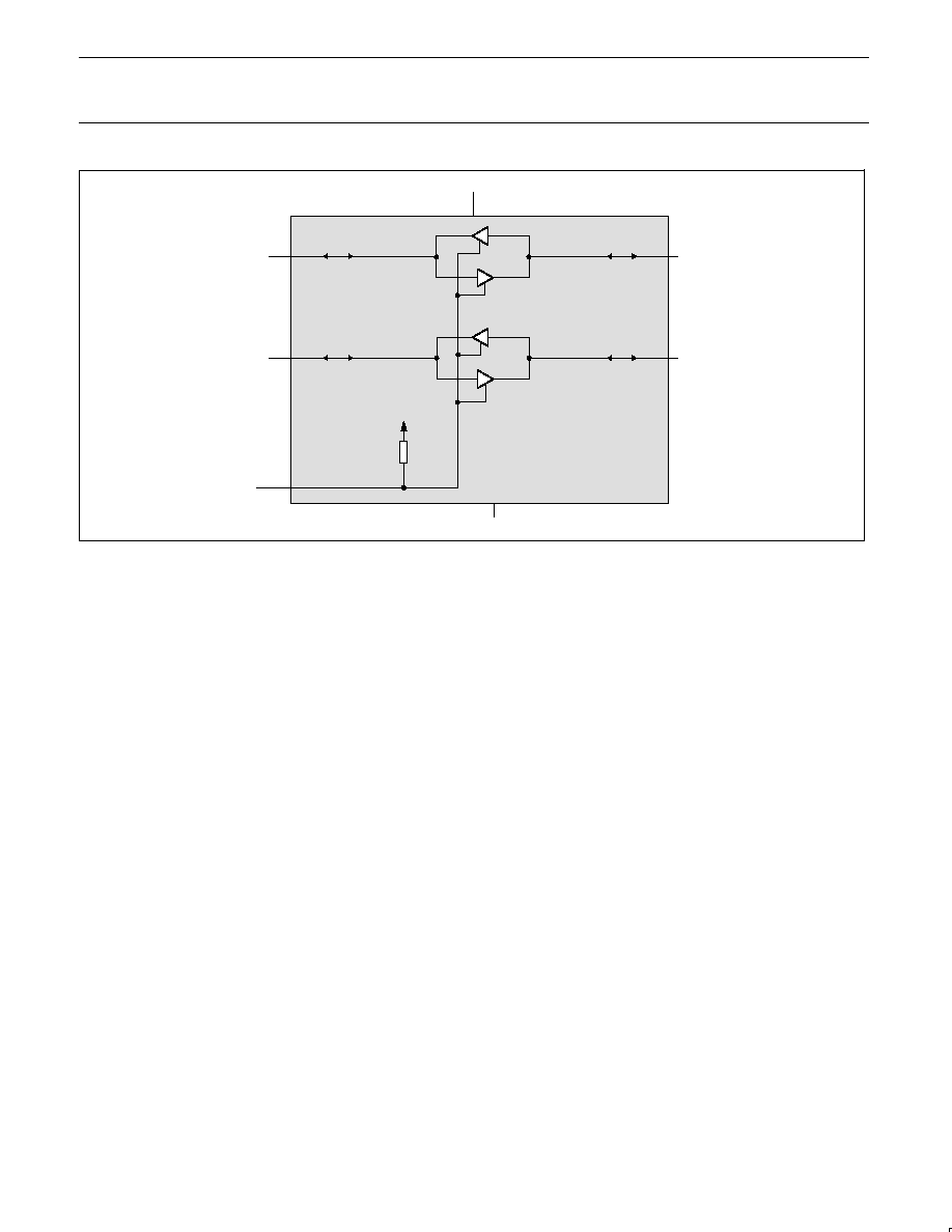
PCA9515A
V
CC
SDA1
SCL1
SCL0
SDA0
SW02244
PULL-UP
RESISTOR
EN
GND
Figure 2. PCA9515A block diagram
The output pull-down of each internal buffer is set for approximately
0.5 V, while the input threshold of each internal buffer is set about
0.07 V lower, when the output is internally driven LOW. This
prevents a lock-up condition from occurring.
FUNCTIONAL DESCRIPTION
The PCA9515A integrated circuit contains two identical buffer
circuits which enable I
2
C and similar bus systems to be extended
without degradation of system performance.
The PCA9515A contains two bi-directional, open drain buffers
specifically designed to support the standard LOW-level-contention
arbitration of the I
2
C-bus. Except during arbitration or clock
stretching, the PCA9515A acts like a pair of non-inverting, open
drain buffers, one for SDA and one for SCL.
Enable
The EN pin is active HIGH with an internal pull up and allows the
user to select when the repeater is active. This can be used to
isolate a badly behaved slave on power up until after the system
power up reset. It should never change state during an I
2
C
operation because disabling during a bus operation will hang the
bus and enabling part way through a bus cycle could confuse the
I
2
C parts being enabled.
The enable pin should only change state when the global bus and
the repeater port are in an idle state to prevent system failures.
I
2
C Systems
As with the standard I
2
C system, pull-up resistors are required to
provide the logic HIGH levels on the Buffered bus. (Standard
open-collector configuration of the I
2
C-bus). The size of these
pull-up resistors depends on the system, but each side of the
repeater must have a pull-up resistor. This part designed to work
with standard mode and fast mode I
2
C devices in addition to SMBus
devices. Standard mode I
2
C devices only specify 3 mA output drive,
this limits the termination current to 3 mA in a generic I
2
C system
where standard mode devices and multiple masters are possible.
Under certain conditions higher termination currents can be used.
Please see Application Note AN255
"I
2
C & SMBus Repeaters, Hubs
and Expanders" for additional information on sizing resistors and
precautions when using more than one PCA9515A/PCA9516A in a
system or using the PCA9515A/16A in conjunction with the P82B96.
Philips Semiconductors
Product data sheet
PCA9515A
I
2
C-bus repeater
2004 Sep 29
4
APPLICATION INFORMATION
A typical application is shown in Figure 3. In this example, the
system master is running on a 3.3 V I
2
C-bus while the slave is
connected to a 5 V bus. Both buses run at 100 kHz unless the slave
bus is isolated and then the master bus can run at 400 kHz. Master
devices can be placed on either bus.
SW02245
BUS0
BUS
MASTER
400 kHz
SLAVE
100 kHz
PCA9515A
SDA
SDA0
SDA
SCL
SCL0
SCL
EN
BUS1
3.3 V
5 V
SDA1
SCL1
Figure 3. Typical application
The PCA9515A is 5 V tolerant so it does not require any additional
circuitry to translate between the different bus voltages.
When one side of the PCA9515A is pulled LOW by a device on the
I
2
C-bus, a CMOS hysteresis type input detects the falling edge and
causes an internal driver on the other side to turn on, thus causing
the other side to also go LOW. The side driven LOW by the
PCA9515A will typically be at V
OL
= 0.5 V.
In order to illustrate what would be seen in a typical application, refer
to Figures 4 and 5. If the bus master in Figure 3 were to write to the
slave through the PCA9515A, we would see the waveform shown in
Figure 4 on Bus 0. This looks like a normal I
2
C transmission until the
falling edge of the 8
th
clock pulse. At that point, the master releases
the data line (SDA) while the slave pulls it LOW through the
PCA9515A. Because the V
OL
of the PCA9515A is typically around
0.5 V, a step in the SDA will be seen. After the master has
transmitted the 9
th
clock pulse, the slave releases the data line.
9th CLOCK PULSE
V
OL
OF MASTER
V
OL
OF PCA9515A
2 V/DIV
SW02247
Figure 4. Bus 0 waveform

Philips Semiconductors
Product data sheet
PCA9515A
I
2
C-bus repeater
2004 Sep 29
5
On the Bus 1 side of the PCA9515A, the clock and data lines would
have a positive offset from ground equal to the V
OL
of the
PCA9515A. After the 8
th
clock pulse, the data line will be pulled to
the V
OL
of the slave device that is very close to ground in our
example.
It is important to note that any arbitration or clock stretching events
on Bus 1 require that the V
OL
of the devices on Bus 1 be 70 mV
below the V
OL
of the PCA9515A (see V
OL
V
ilc
in the DC
Characteristics section) to be recognized by the PCA9515A and
then transmitted to Bus 0.
9th CLOCK PULSE
V
OL
OF SLAVE
V
OL
OF PCA9515A
2 V/DIV
SW02246
Figure 5. Bus 1 waveform
Philips Semiconductors
Product data sheet
PCA9515A
I
2
C-bus repeater
2004 Sep 29
6
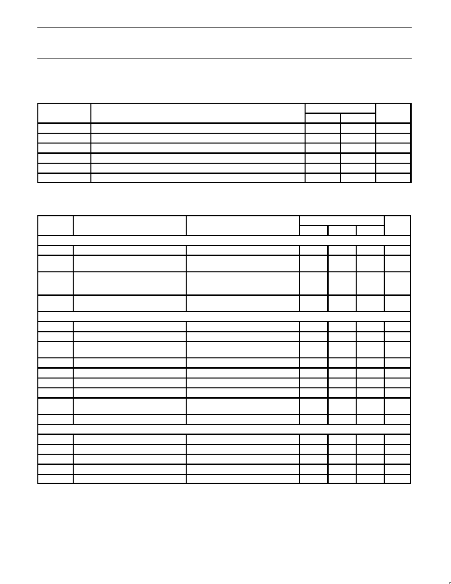
ABSOLUTE MAXIMUM RATINGS
Limiting values in accordance with the Absolute Maximum System (IEC 134).
Voltages with respect to pin GND.
SYMBOL
PARAMETER
LIMITS
UNIT
SYMBOL
PARAMETER
MIN.
MAX.
UNIT
V
CC
to GND
Supply voltage range V
CC
0.5
+7
V
V
bus
Voltage range I
2
C-bus, SCL or SDA
0.5
+7
V
I
DC current (any pin)
--
50
mA
P
tot
Power dissipation
--
100
mW
T
stg
Storage temperature range
55
+125
°
C
T
amb
Operating ambient temperature range
40
+85
°
C
DC ELECTRICAL CHARACTERISTICS
V
CC
= 3.0 V to 3.6 V; GND = 0 V; T
amb
= 40 to +85
°
C; unless otherwise specified.
SYMBOL
PARAMETER
TEST CONDITIONS
LIMITS
UNIT
SYMBOL
PARAMETER
TEST CONDITIONS
MIN.
TYP.
2
MAX.
UNIT
Supplies
V
CC
DC supply voltage
3.0
--
3.6
V
I
CCH
Quiescent supply current,
both channels HIGH
V
CC
= 3.6 V;
SDAn = SCLn = V
CC
--
0.8
5
mA
I
CCL
Quiescent supply current,
both channels LOW
V
CC
= 3.6 V;
one SDA and one SCL = GND,
other SDA and SCL open
--
1.7
5
mA
I
CCLc
Quiescent supply current in contention
V
CC
= 3.6 V;
SDAn = SCLn = GND
--
1.6
5
mA
Input SCL; input/output SDA
V
IH
HIGH-level input voltage
0.7 V
CC
--
5.5
V
V
IL
LOW-level input voltage (Note 1)
0.5
--
0.3 V
CC
V
V
ILc
LOW-level input voltage contention
(Note 1)
0.5
--
0.4
V
V
IK
Input clamp voltage
I
I
= 18 mA
--
--
1.2
V
I
LI
Input leakage current
V
I
= 3.6 V
1
--
+1
µ
A
I
IL
Input current LOW, SDA, SCL
V
I
= 0.2 V, SDA, SCL
--
--
5
µ
A
V
OL
LOW-level output voltage
I
OL
= 20
µ
A or 6 mA
0.47
0.52
0.6
V
V
OL
V
ILc
LOW-level input voltage below
output LOW level voltage
Guaranteed by design
--
--
70
mV
C
I
Input capacitance
V
I
= 3 V or 0 V
--
6
7
pF
Enable
V
IL
LOW-level input voltage
0.5
--
0.8
V
V
IH
HIGH-level input voltage
2.0
--
5.5
V
I
IL
Input current LOW, EN
V
I
= 0.2 V, EN
--
10
30
µ
A
I
LI
Input leakage current
1
--
1
µ
A
C
I
Input capacitance
V
I
= 3.0 V or 0 V
--
6
7
pF
NOTES:
1. V
IL
specification is for the first LOW level seen by the SDAx/SCLx lines. V
ILc
is for the second and subsequent LOW levels seen by the
SDAx/SCLx lines.
2. Typical value taken at 3.3 V and 25
°
C.
3. For operation between published voltage ranges, refer to worst case parameter in both ranges.
Philips Semiconductors
Product data sheet
PCA9515A
I
2
C-bus repeater
2004 Sep 29
7
DC ELECTRICAL CHARACTERISTICS
V
CC
= 2.3 to 2.7 V; GND = 0 V; T
amb
= 40 to +85
°
C; unless otherwise specified.
SYMBOL
PARAMETER
TEST CONDITIONS
LIMITS
UNIT
SYMBOL
PARAMETER
TEST CONDITIONS
MIN.
TYP.
2
MAX.
UNIT
Supplies
V
CC
DC supply voltage
2.3
--
2.7
V
I
CCH
Quiescent supply current,
both channels HIGH
V
CC
= 2.7 V;
SDAn = SCLn = V
CC
--
0.8
5
mA
I
CCL
Quiescent supply current,
both channels LOW
V
CC
= 2.7 V;
one SDA and one SCL = GND,
other SDA and SCL open
--
1.6
5
mA
I
CCLc
Quiescent supply current in contention
V
CC
= 2.7 V;
SDAn = SCLn = GND
--
1.6
5
mA
Input SCL; input/output SDA
V
IH
HIGH-level input voltage
0.7 V
CC
--
5.5
V
V
IL
LOW-level input voltage (Note 1)
0.5
--
0.3 V
CC
V
V
ILc
LOW-level input voltage contention
(Note 1)
0.5
--
0.4
V
V
IK
Input clamp voltage
I
I
= 18 mA
--
--
1.2
V
I
LI
Input leakage current
V
I
= 2.7 V
1
--
+1
µ
A
I
IL
Input current LOW, SDA, SCL
V
I
= 0.2 V, SDA, SCL
--
--
10
µ
A
V
OL
LOW-level output voltage
I
OL
= 20
µ
A or 6 mA
0.47
0.52
0.6
V
V
OL
V
ILc
LOW-level input voltage below
output LOW level voltage
Guaranteed by design
--
--
70
mV
C
I
Input capacitance
V
I
= 3 V or 0 V
--
6
7
pF
Enable
V
IL
LOW-level input voltage
0.5
--
0.8
V
V
IH
HIGH-level input voltage
2.0
--
5.5
V
I
IL
Input current LOW, EN
V
I
= 0.2 V, EN
--
10
30
µ
A
I
LI
Input leakage current
1
--
1
µ
A
C
I
Input capacitance
V
I
= 3.0 V or 0 V
--
6
7
pF
NOTES:
1. V
IL
specification is for the first LOW level seen by the SDAx/SCLx lines. V
ILc
is for the second and subsequent LOW levels seen by the
SDAx/SCLx lines.
2. Typical value taken at 2.5 V and 25
°
C.
Philips Semiconductors
Product data sheet
PCA9515A
I
2
C-bus repeater
2004 Sep 29
8
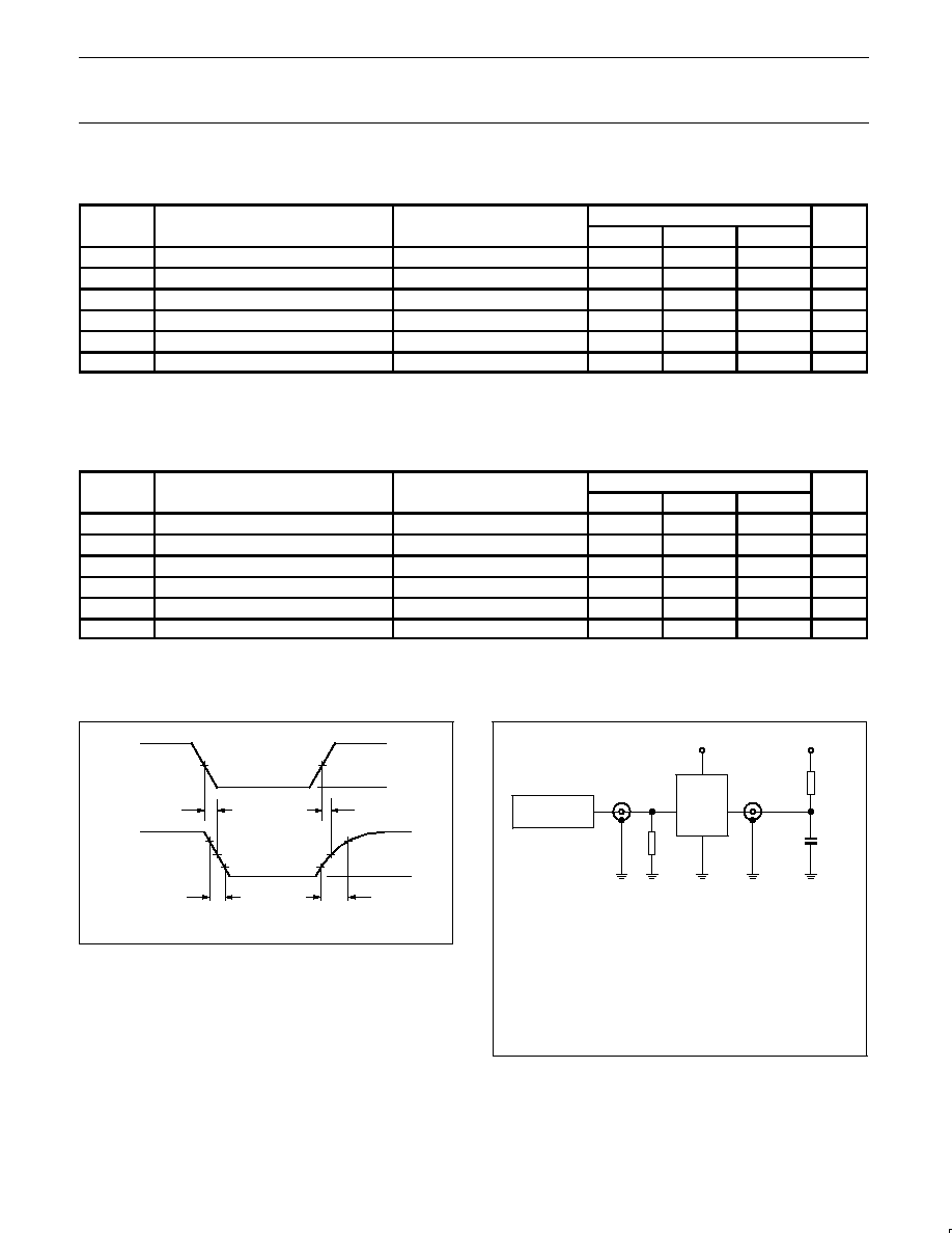
AC ELECTRICAL CHARACTERISTICS
V
CC
= 2.3 to 2.7 V
SYMBOL
PARAMETER
TEST CONDITIONS
LIMITS
UNIT
SYMBOL
PARAMETER
TEST CONDITIONS
MIN.
TYP.
2
MAX.
UNIT
t
PHL
Propagation delay
Waveform 1
45
82
130
ns
t
PLH
Propagation delay
Waveform 1; Note 1
33
113
190
ns
t
THL
Transition time
Waveform 1
--
57
--
ns
t
TLH
Transition time
Waveform 1; Note 1
--
148
--
ns
t
SET
Enable to Start condition
100
--
--
ns
t
HOLD
Enable after Stop condition
130
--
--
ns
NOTES:
1. Different load resistance and capacitance will alter the RC time constant, thereby changing the propagation delay and transition times.
2. Typical value taken at 2.5 V and 25
°
C.
AC ELECTRICAL CHARACTERISTICS
V
CC
= 3.0 to 3.6 V
SYMBOL
PARAMETER
TEST CONDITIONS
LIMITS
UNIT
SYMBOL
PARAMETER
TEST CONDITIONS
MIN.
TYP.
2
MAX.
UNIT
t
PHL
Propagation delay
Waveform 1
45
68
120
ns
t
PLH
Propagation delay
Waveform 1; Note 1
33
102
180
ns
t
THL
Transition time
Waveform 1
--
58
--
ns
t
TLH
Transition time
Waveform 1; Note 1
--
147
--
ns
t
SET
Enable to Start condition
100
--
--
ns
t
HOLD
Enable after Stop condition
100
--
--
ns
NOTES:
1. Different load resistance and capacitance will alter the RC time constant, thereby changing the propagation delay and transition times.
2. Typical value taken at 3.3 V and 25
°
C.
AC WAVEFORMS
3.3 V
0.1 V
1.5 V
1.5 V
INPUT
OUTPUT
3.3 V
V
OL
t
PHL
t
PLH
80%
20%
1.5 V
1.5 V
80%
20%
t
THL
t
TLH
SW00646
Waveform 1.
TEST CIRCUIT
DEFINITIONS
R
L
=
Load resistor; 1.35 k
C
L
=
Load capacitance includes jig and probe capacitance;
50 pF
R
T
=
Termination resistance should be equal to Z
OUT
of
pulse generators.
PULSE
GENERATOR
V
IN
D.U.T.
V
OUT
C
L
V
CC
R
L
Test Circuit for Open Drain Outputs
R
T
SW02280
V
CC
Philips Semiconductors
Product data sheet
PCA9515A
I
2
C-bus repeater
2004 Sep 29
9
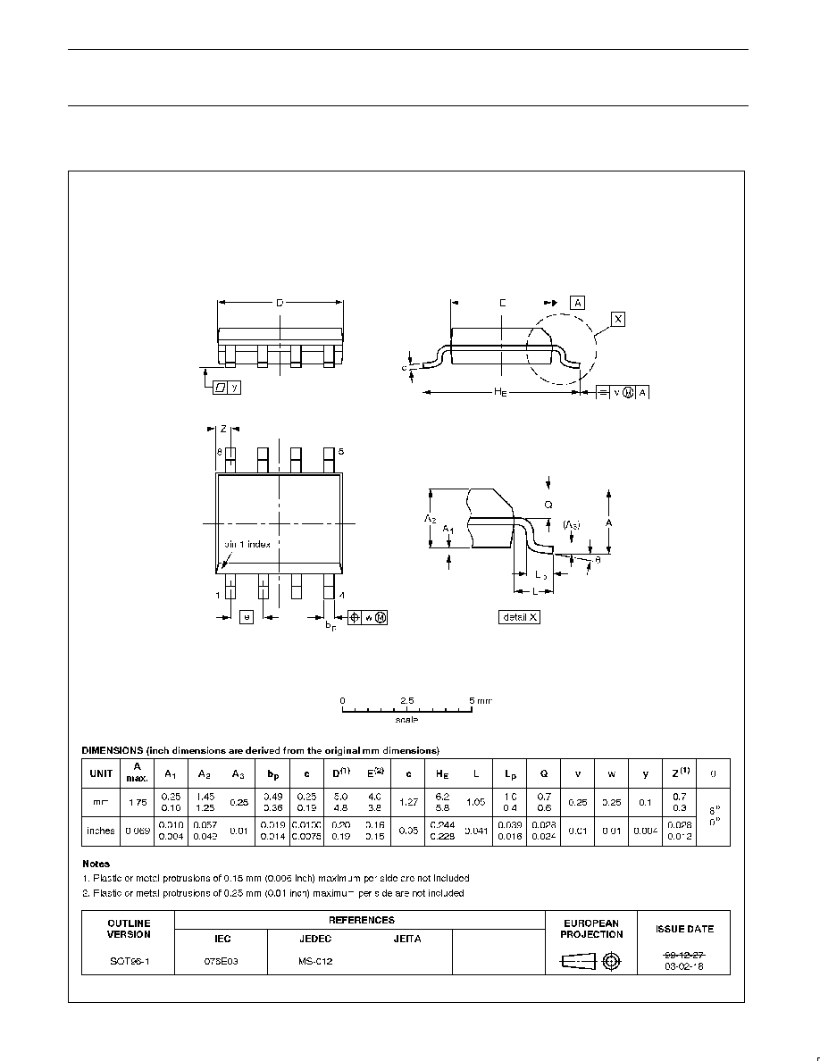
SO8:
plastic small outline package; 8 leads; body width 3.9 mm
SOT96-1
Philips Semiconductors
Product data sheet
PCA9515A
I
2
C-bus repeater
2004 Sep 29
10
TSSOP8:
plastic thin shrink small outline package; 8 leads; body width 3 mm
SOT505-1

Philips Semiconductors
Product data sheet
PCA9515A
I
2
C-bus repeater
2004 Sep 29
11
REVISION HISTORY
Rev
Date
Description
_3
20040929
Product data sheet (9397 750 14098). Supersedes data of 2004 Jul 09 (9397 750 13709).
Modifications:
·
`Features' section on page 2, last bullet: add "(MSOP)"
·
`Ordering information' table on page 2: add "(MSOP)" to 8-pin plastic TSSOP
_2
20040709
Product data sheet (9397 750 13709). Supersedes data of 2004 Jun 17 (9397 750 13237).
_1
20040617
Objective data sheet (9397 750 13237).
Philips Semiconductors
Product data sheet
PCA9515A
I
2
C-bus repeater
2004 Sep 29
12
Purchase of Philips I
2
C components conveys a license under the Philips' I
2
C patent
to use the components in the I
2
C system provided the system conforms to the
I
2
C specifications defined by Philips. This specification can be ordered using the
code 9398 393 40011.
Definitions
Short-form specification -- The data in a short-form specification is extracted from a full data sheet with the same type number and title. For detailed information see
the relevant data sheet or data handbook.
Limiting values definition -- Limiting values given are in accordance with the Absolute Maximum Rating System (IEC 60134). Stress above one or more of the limiting
values may cause permanent damage to the device. These are stress ratings only and operation of the device at these or at any other conditions above those given
in the Characteristics sections of the specification is not implied. Exposure to limiting values for extended periods may affect device reliability.
Application information -- Applications that are described herein for any of these products are for illustrative purposes only. Philips Semiconductors make no
representation or warranty that such applications will be suitable for the specified use without further testing or modification.
Disclaimers
Life support -- These products are not designed for use in life support appliances, devices, or systems where malfunction of these products can reasonably be
expected to result in personal injury. Philips Semiconductors customers using or selling these products for use in such applications do so at their own risk and agree
to fully indemnify Philips Semiconductors for any damages resulting from such application.
Right to make changes -- Philips Semiconductors reserves the right to make changes in the products--including circuits, standard cells, and/or software--described
or contained herein in order to improve design and/or performance. When the product is in full production (status `Production'), relevant changes will be communicated
via a Customer Product/Process Change Notification (CPCN). Philips Semiconductors assumes no responsibility or liability for the use of any of these products, conveys
no license or title under any patent, copyright, or mask work right to these products, and makes no representations or warranties that these products are free from patent,
copyright, or mask work right infringement, unless otherwise specified.
Contact information
For additional information please visit
http://www.semiconductors.philips.com.
Fax: +31 40 27 24825
For sales offices addresses send e-mail to:
sales.addresses@www.semiconductors.philips.com.
©
Koninklijke Philips Electronics N.V. 2004
All rights reserved. Published in the U.S.A.
Date of release: 09-04
Document number:
9397 750 14098
Philips
Semiconductors
Data sheet status
[1]
Objective data sheet
Preliminary data sheet
Product data sheet
Product
status
[2] [3]
Development
Qualification
Production
Definitions
This data sheet contains data from the objective specification for product development.
Philips Semiconductors reserves the right to change the specification in any manner without notice.
This data sheet contains data from the preliminary specification. Supplementary data will be published
at a later date. Philips Semiconductors reserves the right to change the specification without notice, in
order to improve the design and supply the best possible product.
This data sheet contains data from the product specification. Philips Semiconductors reserves the
right to make changes at any time in order to improve the design, manufacturing and supply. Relevant
changes will be communicated via a Customer Product/Process Change Notification (CPCN).
Data sheet status
[1] Please consult the most recently issued data sheet before initiating or completing a design.
[2] The product status of the device(s) described in this data sheet may have changed since this data sheet was published. The latest information is available on the Internet at URL
http://www.semiconductors.philips.com.
[3] For data sheets describing multiple type numbers, the highest-level product status determines the data sheet status.
Level
I
II
III