
1.
General description
The PCA9502 is an 8-bit I/O expander with I
2
C-bus/SPI host interface. The device comes
in a very small HVQFN24 package, which makes it ideally suitable for hand-held, battery
operated applications.
The device also supports software reset, which allows the host to reset the device at any
time, independent of the hardware reset signal.
2.
Features
2.1 General features
I
Selectable I
2
C-bus or SPI interface
I
3.3 V or 2.5 V operation
I
Industrial temperature range:
-
40
�
C to +85
�
C
I
Eight programmable I/O pins
I
Software reset
I
Industrial and commercial temperature ranges
I
Available in HVQFN24 package
I
16 hardware-selectable slave addresses
2.2 I
2
C-bus features
I
Noise filter on SCL/SDA inputs
I
400 kbit/s (maximum)
I
Compliant with I
2
C-bus Fast-mode
I
Slave mode only
2.3 SPI features
I
15 Mbit/s maximum speed
I
Slave mode only
I
SPI Mode 0
3.
Applications
I
Factory automation and process control
I
Portable and battery operated devices
I
Cellular data devices
PCA9502
8-bit I/O expander with I
2
C-bus/SPI interface
Rev. 02 -- 3 August 2006
Product data sheet
PCA9502_2
� Koninklijke Philips Electronics N.V. 2006. All rights reserved.
Product data sheet
Rev. 02 -- 3 August 2006
2 of 24
Philips Semiconductors
PCA9502
8-bit I/O expander with I
2
C-bus/SPI interface
4.
Ordering information
5.
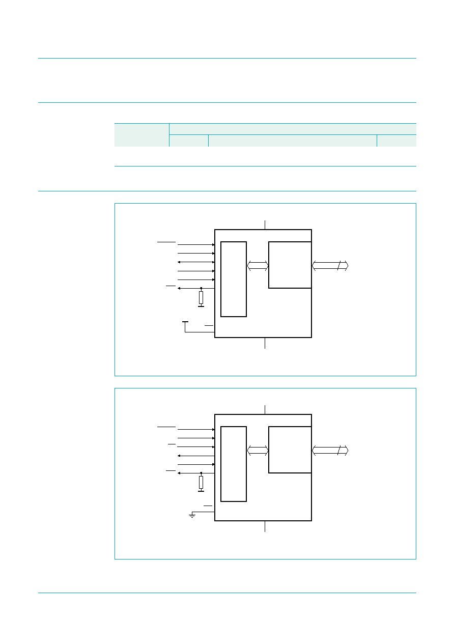
Block diagram
Table 1.
Ordering information
Type number
Package
Name
Description
Version
PCA9502BS
HVQFN24
plastic thermal enhanced very thin quad flat package;
no leads; 24 terminals; body 4
�
4
�
0.85 mm
SOT616-3
Fig 1.
Block diagram of PCA9502 I
2
C-bus interface
Fig 2.
Block diagram of PCA9502 SPI interface
PCA9502
002aab837
V
DD
I
2
C-BUS
GPIO
REGISTER
GPIO[7:0]
SCL
SDA
A0
IRQ
I2C/SPI
8
A1
RESET
V
DD
V
SS
V
DD
1 k
(3.3 V)
1.5 k
(2.5 V)
CS
PCA9502
002aab838
SPI
GPIO
REGISTER
GPIO[7:0]
SCLK
SO
IRQ
I2C/SPI
8
SI
RESET
V
DD
V
SS
V
DD
1 k
(3.3 V)
1.5 k
(2.5 V)
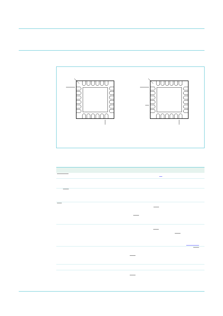
PCA9502_2
� Koninklijke Philips Electronics N.V. 2006. All rights reserved.
Product data sheet
Rev. 02 -- 3 August 2006
3 of 24
Philips Semiconductors
PCA9502
8-bit I/O expander with I
2
C-bus/SPI interface
6.
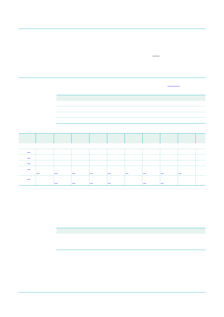
Pinning information
6.1 Pinning
6.2 Pin description
a. I
2
C-bus interface
b. SPI interface
Fig 3.
Pin configuration for HVQFN24
GPIO7
GPIO6
GPIO5
GPIO4
V
SS
GPIO2
GPIO1
GPIO0
SCL
n.c.
A1
A0
V
DD
V
DD
RESET
V
DD
GPIO3
V
DD
V
SS
SDA
002aab839
Transparent top view
V
DD
V
SS
V
DD
terminal 1
index area
6
13
5
14
4
15
3
16
2
17
1
18
7
8
9
10
11
12
24
23
22
21
20
19
PCA9502BS
IRQ
GPIO7
GPIO6
GPIO5
GPIO4
V
SS
GPIO2
GPIO1
GPIO0
SCLK
SO
SI
CS
V
SS
V
DD
RESET
V
DD
GPIO3
V
DD
V
SS
V
SS
002aab840
Transparent top view
V
DD
V
SS
V
DD
terminal 1
index area
6
13
5
14
4
15
3
16
2
17
1
18
7
8
9
10
11
12
24
23
22
21
20
19
PCA9502BS
IRQ
Table 2.
Pin description
Symbol
Pin
Type
Description
RESET
1
I
device hardware reset (active LOW)
[1]
V
DD
2, 3, 11,
22, 24
-
power supply
I2C/SPI
4
I
I
2
C-bus or SPI interface select. I
2
C-bus interface is selected if this
pin is at logic HIGH. SPI interface is selected if this pin is at logic
LOW.
CS/A0
5
I
SPI chip select or I
2
C-bus device address select A0. If SPI
configuration is selected by I2C/SPI pin, this pin is the SPI chip
select pin (Schmitt trigger, active LOW). If I
2
C-bus configuration
is selected by I2C/SPI pin, this pin along with A1 pin allows user
to change the device's base address.
SI/A1
6
I
SPI data input pin or I
2
C-bus device address select A1. If SPI
configuration is selected by I2C/SPI pin, this is the SPI data input
pin. If I
2
C-bus configuration is selected by I2C/SPI pin, this pin
along with A0 pin allows user to change the device's base
address. To select the device address, please refer to
Table 11
.
SO
7
O
SPI data output pin. If SPI configuration is selected by I2C/SPI
pin, this is a 3-stateable output pin. If I
2
C-bus configuration is
selected by I2C/SPI pin, this pin function is undefined and must
be left as n.c. (not connected).
SCL/SCLK
8
I
I
2
C-bus or SPI input clock.
SDA
9
I/O
I
2
C-bus data input/output, open-drain if I
2
C-bus configuration is
selected by I2C/SPI pin. If SPI configuration is selected then this
pin is an undefined pin and must be connected to V
SS
.

PCA9502_2
� Koninklijke Philips Electronics N.V. 2006. All rights reserved.
Product data sheet
Rev. 02 -- 3 August 2006
4 of 24
Philips Semiconductors
PCA9502
8-bit I/O expander with I
2
C-bus/SPI interface
[1]
See
Section 7.1 "Hardware reset, Power-On Reset (POR) and software reset"
7.
Functional description
The device interfaces to a host through either I
2
C-bus or SPI interface (selectable through
I2C/SPI pin), and provides the host with eight programmable GPIO pins.
7.1 Hardware reset, Power-On Reset (POR) and software reset
These three reset methods are identical and will reset the internal registers as indicated in
Table 3
.
Table 3
summarizes the state of registers after reset.
Table 4
summarizes the state of hardware pins after reset.
IRQ
12
O
Interrupt (open-drain, active LOW). Interrupt is enabled when
interrupt sources are enabled in the I/O Interrupt Enable register
(IOIntEna). The interrupt condition is the change of state of the
input pins. An external resistor (1 k
for 3.3 V, 1.5 k
for 2.5 V)
must be connected between this pin and V
DD
.
GPIO0
13
I/O
programmable I/O pin
GPIO1
14
I/O
programmable I/O pin
GPIO2
15
I/O
programmable I/O pin
GPIO3
16
I/O
programmable I/O pin
GPIO4
18
I/O
programmable I/O pin
GPIO5
19
I/O
programmable I/O pin
GPIO6
20
I/O
programmable I/O pin
GPIO7
21
I/O
programmable I/O pin
V
SS
10, 17,
23
-
ground
V
SS
center
pad
-
The center pad on the back side of the HVQFN24 package is
metallic and should be connected to ground on the printed-circuit
board.
Table 2.
Pin description
...continued
Symbol
Pin
Type
Description
Table 3.
Registers after reset
Register
Reset state
I/O direction
all bits cleared
I/O interrupt enable
all bits cleared
I/O control
all bits cleared
Table 4.
Signals after reset
Signal
Reset state
I/Os
inputs
IRQ
HIGH by external pull-up
PCA9502_2
� Koninklijke Philips Electronics N.V. 2006. All rights reserved.
Product data sheet
Rev. 02 -- 3 August 2006
5 of 24
Philips Semiconductors
PCA9502
8-bit I/O expander with I
2
C-bus/SPI interface
7.2 Interrupts
The PCA9502 has interrupt generation capability. The interrupt enable register (IOIntEna)
enables interrupts due to I/O pin change of state, and the IRQ signal in response to an
interrupt generation.
8.
Register descriptions
The programming combinations for register selection are shown in
Table 5
.
[1]
Other addresses 0x00 through 0x09, 0x0F are reserved and should not be accessed (read or write).
[2]
These bits are reserved and should be set to 0.
8.1 Programmable I/O pins Direction register (IODir)
This register is used to program the I/O pins direction. Bit 0 to bit 7 control GPIO0 to
GPIO7.
Remark: If there is a pending input (GPIO) interrupt and IODir is written, this pending
interrupt will be cleared, that is, the interrupt signal will be negated.
Table 5.
Register map - read/write properties
Register name
Read mode
Write mode
IODir
I/O pin direction
I/O pin direction
IOState
I/O pin states
n/a
IOIntEna
I/O interrupt enable register
I/O interrupt enable register
IOControl
I/O pins control
I/O pins control
Table 6.
PCA9502 internal registers
Register
address
Register
Bit 7
Bit 6
Bit 5
Bit 4
Bit 3
Bit 2
Bit 1
Bit 0
R/W
General Register Set
0x0A
[1]
IODir
bit 7
bit 6
bit 5
bit 4
bit 3
bit 2
bit 1
bit 0
R/W
0x0B
[1]
IOState
bit 7
bit 6
bit 5
bit 4
bit 3
bit 2
bit 1
bit 0
R/W
0x0C
[1]
IOIntEna
bit 7
bit 6
bit 5
bit 4
bit 3
bit 2
bit 1
bit 0
R/W
0x0D
[1]
reserved
[2]
reserved
[2]
reserved
[2]
reserved
[2]
reserved
[2]
reserved
[2]
reserved
[2]
reserved
[2]
reserved
[2]
0x0E
[1]
IOControl
reserved
[2]
reserved
[2]
reserved
[2]
reserved
[2]
SReset
reserved
[2]
reserved
[2]
IOLatch
R/W
Table 7.
IODir register (address 0x0A) bit description
Bit
Symbol
Description
7:0
IODir
set GPIO pins 7:0 to input or output
0 = input
1 = output

PCA9502_2
� Koninklijke Philips Electronics N.V. 2006. All rights reserved.
Product data sheet
Rev. 02 -- 3 August 2006
6 of 24
Philips Semiconductors
PCA9502
8-bit I/O expander with I
2
C-bus/SPI interface
8.2 Programmable I/O pins State register (IOState)
When `read', this register returns the actual state of all I/O pins. When `write', each
register bit will be transferred to the corresponding IO pin programmed as output.
8.3 I/O Interrupt Enable register (IOIntEna)
This register enables the interrupt due to a change in the I/O configured as inputs.
8.4 I/O Control register (IOControl)
Table 8.
IOState register (address 0x0B) bit description
Bit
Symbol
Description
7:0
IOState
Write this register: set the logic level on the output pins
0 = set output pin to zero
1 = set output pin to one
Read this register: return states of all pins
Table 9.
IOIntEna register (address 0x0C) bit description
Bit
Symbol
Description
7:0
IOIntEna
input interrupt enable
0 = a change in the input pin will not generate an interrupt
1 = a change in the input will generate an interrupt
Table 10.
IOControl register (address 0x0E) bit description
Bit
Symbol
Description
7:4
-
reserved for future use
3
SReset
software reset
A write to this bit will reset the device. Once the device is reset this
bit is automatically set to 0.
2:1
-
reserved for future use
0
IOLatch
enable/disable inputs latching
0 = input values are not latched. A change in any input generates an
interrupt. A read of the input register clears the interrupt. If the input
goes back to its initial logic state before the input register is read,
then the interrupt is cleared.
1 = input values are latched. A change in the input generates an
interrupt and the input logic value is loaded in the bit of the
corresponding input state register (IOState). A read of the IOState
register clears the interrupt. If the input pin goes back to its initial
logic state before the interrupt register is read, then the interrupt is
not cleared and the corresponding bit of the IOState register keeps
the logic value that initiates the interrupt.
Example: If GPIO4 input was as logic 0 and the input goes to logic 1
then back to logic 0, the IOState register will capture this change and
an interrupt is generated (if enabled). When the read is performed on
the IOState register, the interrupt is de-asserted, assuming there were
no additional input(s) that changed, and bit 4 of the IOState register
will read `1'. The next read of the IOState register should now read `0'.
PCA9502_2
� Koninklijke Philips Electronics N.V. 2006. All rights reserved.
Product data sheet
Rev. 02 -- 3 August 2006
7 of 24
Philips Semiconductors
PCA9502
8-bit I/O expander with I
2
C-bus/SPI interface
9.
I
2
C-bus operation
The two lines of the I
2
C-bus are a serial data line (SDA) and a serial clock line (SCL). Both
lines are connected to a positive supply via a pull-up resistor, and remain HIGH when the
bus is not busy. Each device is recognized by a unique address whether it is a
microcomputer, LCD driver, memory or keyboard interface and can operate as either a
transmitter or receiver, depending on the function of the device. A device generating a
message or data is a transmitter, and a device receiving the message or data is a
receiver. Obviously, a passive function like an LCD driver could only be a receiver, while a
microcontroller or a memory can both transmit and receive data.
9.1 Data transfers
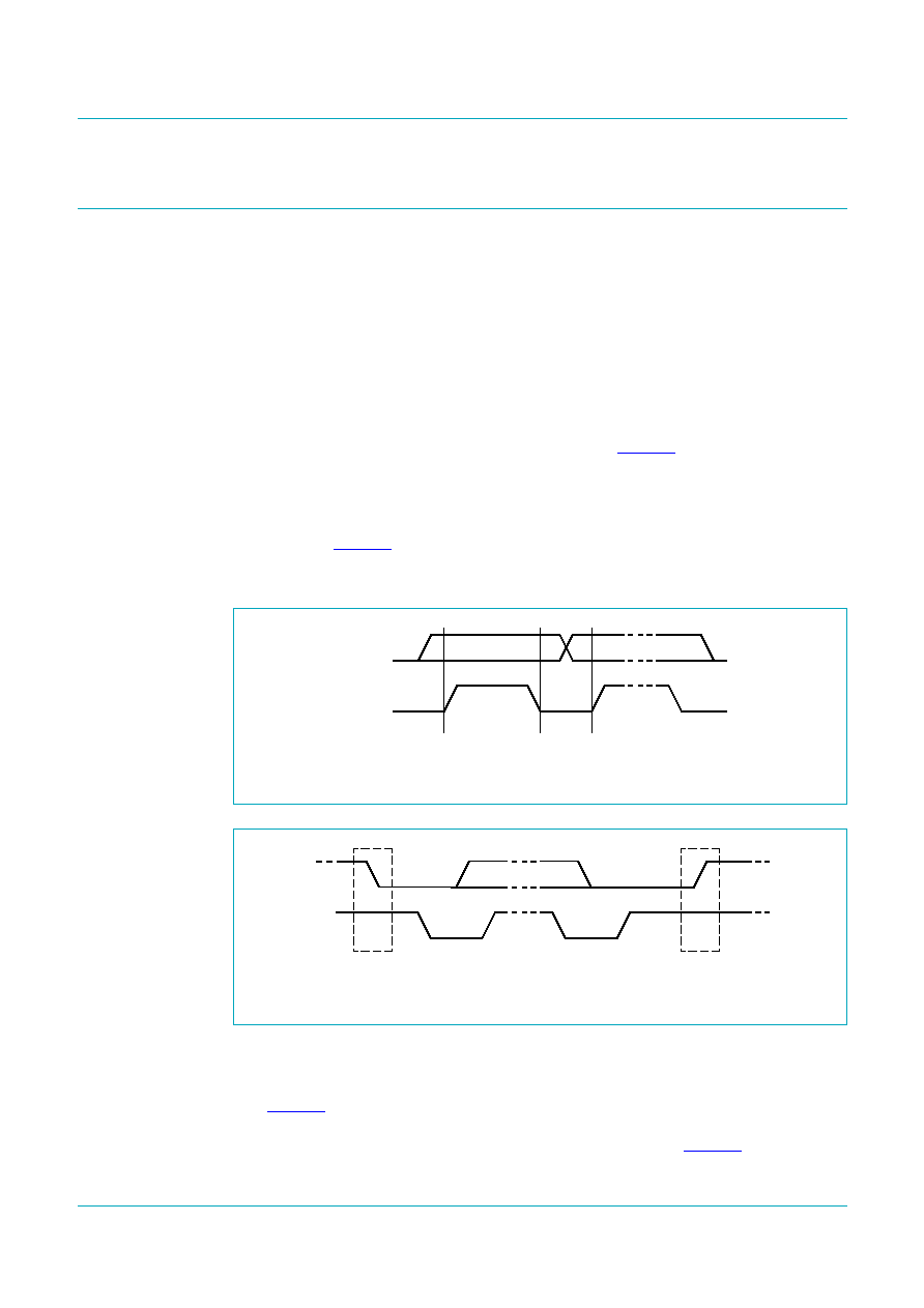
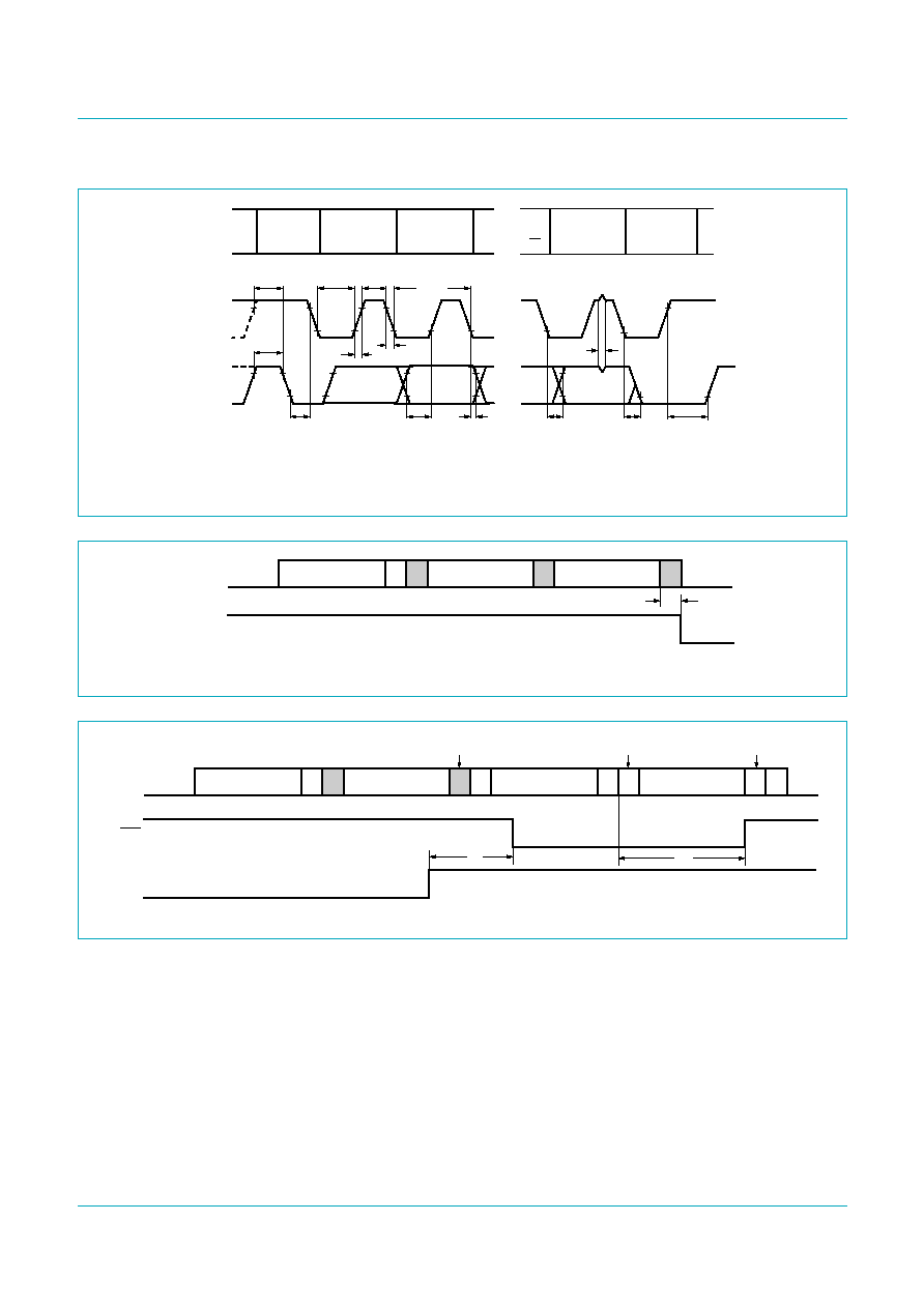
One data bit is transferred during each clock pulse (see
Figure 4
). The data on the SDA
line must remain stable during the HIGH period of the clock pulse in order to be valid.
Changes in the data line at this time will be interpreted as control signals. A HIGH-to-LOW
transition of the data line (SDA) while the clock signal (SCL) is HIGH indicates a START
condition, and a LOW-to-HIGH transition of the SDA while SCL is HIGH defines a STOP
condition (see
Figure 5
). The bus is considered to be busy after the START condition and
free again at a certain time interval after the STOP condition. The START and STOP
conditions are always generated by the master.
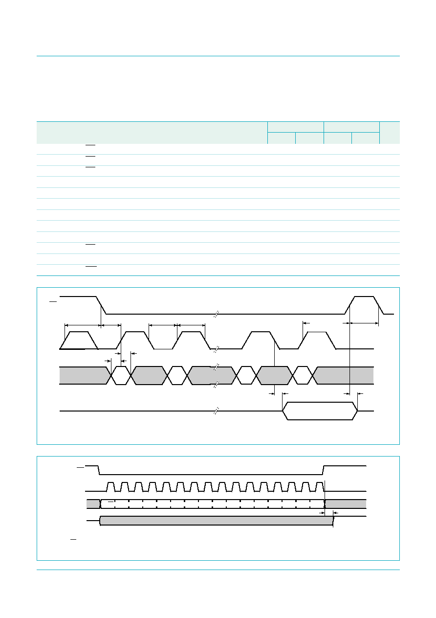
The number of data bytes transferred between the START and STOP condition from
transmitter to receiver is not limited. Each byte, which must be eight bits long, is
transferred serially with the most significant bit first, and is followed by an acknowledge bit.
(see
Figure 6
). The clock pulse related to the acknowledge bit is generated by the master.
The device that acknowledges has to pull down the SDA line during the acknowledge
clock pulse, while the transmitting device releases this pulse (see
Figure 7
).
Fig 4.
Bit transfer on the I
2
C-bus
Fig 5.
START and STOP conditions
mba607
data line
stable;
data valid
change
of data
allowed
SDA
SCL
mba608
SDA
SCL
P
STOP condition
SDA
SCL
S
START condition

PCA9502_2
� Koninklijke Philips Electronics N.V. 2006. All rights reserved.
Product data sheet
Rev. 02 -- 3 August 2006
8 of 24
Philips Semiconductors
PCA9502
8-bit I/O expander with I
2
C-bus/SPI interface
A slave receiver must generate an acknowledge after the reception of each byte, and a
master must generate one after the reception of each byte clocked out of the slave
transmitter.
There is an exception to the `acknowledge after every byte' rule. It occurs when a master
is a receiver: it must signal an end of data to the transmitter by not signalling an
acknowledge on the last byte that has been clocked out of the slave. The acknowledge
related clock, generated by the master should still take place, but the SDA line will not be
pulled down. In order to indicate that this is an active and intentional lack of
acknowledgement, we shall term this special condition as a `negative acknowledge'.
9.2 Addressing and transfer formats
Each device on the bus has its own unique address. Before any data is transmitted on the
bus, the master transmits on the bus the address of the slave to be accessed for this
transaction. A well-behaved slave with a matching address, if it exists on the network,
should of course acknowledge the master's addressing. The addressing is done by the
first byte transmitted by the master after the START condition.
An address on the network is seven bits long, appearing as the most significant bits of the
address byte. The last bit is a direction (R/W) bit. A `0' indicates that the master is
transmitting (write) and a `1' indicates that the master requests data (read). A complete
data transfer, comprised of an address byte indicating a `write' and two data bytes is
shown in
Figure 8
.
Fig 6.
Data transfer on the I
2
C-bus
S
P
SDA
SCL
MSB
0
1
6
7
8
0
1
2 to 7
8
ACK
ACK
002aab012
START
condition
STOP
condition
acknowledgement signal
from receiver
byte complete,
interrupt within receiver
clock line held LOW
while interrupt is serviced
Fig 7.
Acknowledge on the I
2
C-bus
S
0
1
6
7
8
002aab013
data output
by transmitter
data output
by receiver
SCL from master
START
condition
transmitter stays off of the bus
during the acknowledge clock
acknowledgement signal
from receiver
PCA9502_2
� Koninklijke Philips Electronics N.V. 2006. All rights reserved.
Product data sheet
Rev. 02 -- 3 August 2006
9 of 24
Philips Semiconductors
PCA9502
8-bit I/O expander with I
2
C-bus/SPI interface
When an address is sent, each device in the system compares the first seven bits after the
START with its own address. If there is a match, the device will consider itself addressed
by the master, and will send an acknowledge. The device could also determine if in this
transaction it is assigned the role of a slave receiver or slave transmitter, depending on the
R/W bit.
Each node of the I
2
C-bus network has a unique seven-bit address. The address of a
microcontroller is of course fully programmable, while peripheral devices usually have
fixed and programmable address portions.
When the master is communicating with one device only, data transfers follow the format
of
Figure 8
, where the R/W bit could indicate either direction. After completing the transfer
and issuing a STOP condition, if a master would like to address some other device on the
network, it could start another transaction by issuing a new START.
Another way for a master to communicate with several different devices would be by using
a `repeated START'. After the last byte of the transaction was transferred, including its
acknowledge (or negative acknowledge), the master issues another START, followed by
address byte and data, without effecting a STOP. The master may communicate with a
number of different devices, combining `reads' and `writes'. After the last transfer takes
place, the master issues a STOP and releases the bus. Possible data formats are
demonstrated in
Figure 9
. Note that the repeated START allows for both change of a slave
and a change of direction, without releasing the bus. We shall see later on that the change
of direction feature can come in handy even when dealing with a single device.
In a single master system, the repeated START mechanism may be more efficient than
terminating each transfer with a STOP and starting again. In a multimaster environment,
the determination of which format is more efficient could be more complicated, as when a
master is using repeated STARTs it occupies the bus for a long time and thus preventing
other devices from initiating transfers.
Fig 8.
A complete data transfer
S
P
SDA
SCL
0 to 6
7
8
ACK
002aab046
START
condition
STOP
condition
address
R/W
0 to 6
7
8
data
ACK
0 to 6
7
8
data
ACK
PCA9502_2
� Koninklijke Philips Electronics N.V. 2006. All rights reserved.
Product data sheet
Rev. 02 -- 3 August 2006
10 of 24
Philips Semiconductors
PCA9502
8-bit I/O expander with I
2
C-bus/SPI interface
Fig 9.
I
2
C-bus data formats
002aab458
DATA
SLAVE ADDRESS
master write:
S
W
A
DATA
A
A
P
data transferred
(n bytes + acknowledge)
START condition
STOP condition
acknowledge
acknowledge
acknowledge
write
DATA
SLAVE ADDRESS
master read:
S
R
A
DATA
A
NA
P
data transferred
(n bytes + acknowledge)
START condition
STOP condition
acknowledge
acknowledge
not
acknowledge
read
DATA
SLAVE ADDRESS
combined
formats:
S
R/W
A
DATA
A
A
P
data transferred
(n bytes + acknowledge)
START condition
STOP condition
acknowledge
acknowledge
acknowledge
read or
write
SLAVE ADDRESS
Sr
R/W
A
repeated
START condition
acknowledge
read or
write
direction of transfer
may change at this point
data transferred
(n bytes + acknowledge)

PCA9502_2
� Koninklijke Philips Electronics N.V. 2006. All rights reserved.
Product data sheet
Rev. 02 -- 3 August 2006
11 of 24
Philips Semiconductors
PCA9502
8-bit I/O expander with I
2
C-bus/SPI interface
9.3 Addressing
Before any data is transmitted or received, the master must send the address of the
receiver via the SDA line. The first byte after the START condition carries the address of
the slave device and the read/write bit.
Table 11
shows how the PCA9502's address can
be selected by using A1 and A0 pins. For example, if these 2 pins are connected to V
DD
,
then the PCA9502's address is set to 0x90, and the master communicates with it through
this address.
[1]
X = logic 0 for write cycle; X = logic 1 for read cycle.
9.4 Use of sub-addresses
When a master communicates with the PCA9502 it must send a sub-address in the byte
following the slave address byte. This sub-address is the internal address of the word the
master wants to access for a single byte transfer, or the beginning of a sequence of
locations for a multi-byte transfer. A sub-address is an 8-bit byte. Unlike the device
address, it does not contain a direction (R/W) bit, and like any byte transferred on the bus
it must be followed by an acknowledge.
A register write cycle is shown in
Figure 10
. The START is followed by a slave address
byte with the direction bit set to `write', a sub-address byte, a number of data bytes, and a
STOP signal. The sub-address indicates which register the master wants to access. and
the data bytes which follow will be written one after the other to the sub-address location.
Table 11.
PCA9502 address map
A1
A0
PCA9502 I
2
C-bus addresses (hex)
[1]
V
DD
V
DD
0x90 (1001 000X)
V
DD
V
SS
0x92 (1001 001X)
V
DD
SCL
0x94 (1001 010X)
V
DD
SDA
0x96 (1001 011X)
V
SS
V
DD
0x98 (1001 100X)
V
SS
V
SS
0x9A (1001 101X)
V
SS
SCL
0x9C (1001 110X)
V
SS
SDA
0x9E (1001 111X)
SCL
V
DD
0xA0 (1010 000X)
SCL
V
SS
0xA2 (1010 001X)
SCL
SCL
0xA4 (1010 010X)
SCL
SDA
0xA6 (1010 011X)
SDA
V
DD
0xA8 (1010 100X)
SDA
V
SS
0xAA (1010 101X)
SDA
SCL
0xAC (1010 110X)
SDA
SDA
0xAE (1010 111X)
PCA9502_2
� Koninklijke Philips Electronics N.V. 2006. All rights reserved.
Product data sheet
Rev. 02 -- 3 August 2006
12 of 24
Philips Semiconductors
PCA9502
8-bit I/O expander with I
2
C-bus/SPI interface
The register read cycle (see
Figure 11
) commences in a similar manner, with the master
sending a slave address with the direction bit set to `write' with a following sub-address.
Then, in order to reverse the direction of the transfer, the master issues a repeated START
followed again by the device address, but this time with the direction bit set to `read'. The
data bytes starting at the internal sub-address will be clocked out of the device, each
followed by a master-generated acknowledge. The last byte of the read cycle will be
followed by a negative acknowledge, signalling the end of transfer. The cycle is terminated
by a STOP signal.
White block: host to PCA9502
Grey block: PCA9502 to host
Fig 10. Master writes to slave
S
SLAVE ADDRESS
002aab047
W
A
REGISTER ADDRESS
A
nDATA
A
P
White block: host to PCA9502
Grey block: PCA9502 to host
Fig 11. Master read from Slave
S
SLAVE ADDRESS
002aab048
W
A
REGISTER ADDRESS
A
NA
P
S
SLAVE ADDRESS
R
A
nDATA
A
LAST DATA
Table 12.
Register address byte (I
2
C-bus)
Bit
Name
Function
7
-
not used
6:3
A[3:0]
internal register select
2:1
-
not used, set to 0
0
-
not used
PCA9502_2
� Koninklijke Philips Electronics N.V. 2006. All rights reserved.
Product data sheet
Rev. 02 -- 3 August 2006
13 of 24
Philips Semiconductors
PCA9502
8-bit I/O expander with I
2
C-bus/SPI interface
10. SPI operation
11. Limiting values
[1]
5.5 V steady state voltage tolerance on inputs and outputs is valid only when the supply voltage is present.
4.6 V steady state voltage tolerance on inputs and outputs when no supply voltage is present.
R/W = 0; A[3:0] = register address
a. Register write
R/W = 1; A[3:0] = register address
b. Register read
Fig 12. SPI operation
Table 13.
Register address byte (SPI)
Bit
Name
Function
7
R/W
1: read from PCA9502
0: write to PCA9502
6:3
A[3:0]
internal register select
2:1
-
not used, set to 0
0
-
not used
SI
A1
A2
A3
R/W
SCLK
0
A0
X
0
D6
D7
D4
D5
D2
D3
D0
D1
002aab925
SI
A1
A2
A3
R/W
SCLK
0
A0
X
0
SO
D6
D7
D4
D5
D2
D3
D0
D1
002aab926
Table 14.
Limiting values
In accordance with the Absolute Maximum Rating System (IEC 60134).
Symbol
Parameter
Conditions
Min
Max
Unit
V
DD
supply voltage
-
0.3
+4.6
V
V
I
input voltage
any input
-
0.3
+5.5
[1]
V
I
I
input current
any input
-
10
+10
mA
I
O
output current
any output
-
10
+10
mA
P
tot
total power dissipation
-
300
mW
P/out
power dissipation per output
-
50
mW
T
amb
ambient temperature
-
40
+85
�
C
T
stg
storage temperature
-
65
+150
�
C

PCA9502_2
� Koninklijke Philips Electronics N.V. 2006. All rights reserved.
Product data sheet
Rev. 02 -- 3 August 2006
14 of 24
Philips Semiconductors
PCA9502
8-bit I/O expander with I
2
C-bus/SPI interface
12. Static characteristics
Table 15.
Static characteristics
V
DD
= (2.5 V
�
0.2 V) or (3.3 V
�
0.3 V); T
amb
=
-
40
�
C to +85
�
C; unless otherwise specified.
Symbol
Parameter
Conditions
V
DD
= 2.5 V
V
DD
= 3.3 V
Unit
Min
Max
Min
Max
Supplies
V
DD
supply voltage
2.3
2.7
3.0
3.6
V
I
DD
supply current
operating; no load
-
6.0
-
6.0
mA
Inputs I2C/SPI
V
IH
HIGH-level input voltage
1.6
5.5
[1]
2.0
5.5
[1]
V
V
IL
LOW-level input voltage
-
0.6
-
0.8
V
I
L
leakage current
input; V
I
= 0 V or 5.5 V
[1]
-
1
-
1
�
A
C
i
input capacitance
-
3
-
3
pF
Output SO
V
OH
HIGH-level output voltage
I
OH
=
-
400
�
A
1.85
-
-
-
V
I
OH
=
-
4 mA
-
-
2.4
-
V
V
OL
LOW-level output voltage
I
OL
= 1.6 mA
-
0.4
-
-
V
I
OL
= 4 mA
-
-
-
0.4
V
C
o
output capacitance
-
4
-
4
pF
Inputs/outputs GPIO0 to GPIO7
V
IH
HIGH-level input voltage
1.6
5.5
[1]
2.0
5.5
[1]
V
V
IL
LOW-level input voltage
-
0.6
-
0.8
V
V
OH
HIGH-level output voltage
I
OH
=
-
400
�
A
1.85
-
-
-
V
I
OH
=
-
4 mA
-
-
2.4
-
V
V
OL
LOW-level output voltage
I
OL
= 1.6 mA
-
0.4
-
-
V
I
OL
= 4 mA
-
-
-
0.4
V
I
L
leakage current
input; V
I
= 0 V or 5.5 V
[1]
-
1
-
1
�
A
C
o
output capacitance
-
4
-
4
pF
Output IRQ
V
OL
LOW-level output voltage
I
OL
= 1.6 mA
-
0.4
-
-
V
I
OL
= 4 mA
-
-
-
0.4
V
C
o
output capacitance
-
4
-
4
pF
I
2
C-bus input/output SDA
V
IH
HIGH-level input voltage
1.6
5.5
[1]
2.0
5.5
[1]
V
V
IL
LOW-level input voltage
-
0.6
-
0.8
V
V
OL
LOW-level output voltage
I
OL
= 1.6 mA
-
0.4
-
-
V
I
OL
= 4 mA
-
-
-
0.4
V
I
L
leakage current
input; V
I
= 0 V or 5.5 V
[1]
-
10
-
10
�
A
C
o
output capacitance
-
7
-
7
pF

PCA9502_2
� Koninklijke Philips Electronics N.V. 2006. All rights reserved.
Product data sheet
Rev. 02 -- 3 August 2006
15 of 24
Philips Semiconductors
PCA9502
8-bit I/O expander with I
2
C-bus/SPI interface
[1]
5.5 V steady state voltage tolerance on inputs and outputs is valid only when the supply voltage is present. 3.8 V steady state voltage
tolerance on inputs and outputs when no supply voltage is present.
13. Dynamic characteristics
[1]
A detailed description of the I
2
C-bus specification, with applications, is given in brochure
"The I
2
C-bus and how to use it". This brochure
may be ordered using the code 9398 393 40011.
[2]
Minimum SCL clock frequency is limited by the bus time-out feature, which resets the serial bus interface if SDA is held LOW for a
minimum of 25 ms.
I
2
C-bus inputs SCL, CS/A0, SI/A1
V
IH
HIGH-level input voltage
1.6
5.5
[1]
2.0
5.5
[1]
V
V
IL
LOW-level input voltage
-
0.6
-
0.8
V
I
L
leakage current
input; V
I
= 0 V or 5.5 V
[1]
-
10
-
10
�
A
C
i
input capacitance
-
7
-
7
pF
Table 15.
Static characteristics
...continued
V
DD
= (2.5 V
�
0.2 V) or (3.3 V
�
0.3 V); T
amb
=
-
40
�
C to +85
�
C; unless otherwise specified.
Symbol
Parameter
Conditions
V
DD
= 2.5 V
V
DD
= 3.3 V
Unit
Min
Max
Min
Max
Table 16.
I
2
C-bus timing specifications
All the timing limits are valid within the operating supply voltage, ambient temperature range and output load;
V
DD
= (2.5 V
�
0.2 V) or (3.3 V
�
0.3 V); T
amb
=
-
40
�
C to +85
�
C; refer to V
IL
and V
IH
with an input voltage of V
SS
to V
DD
.
All output load = 25 pF, except SDA output load = 400 pF.
[1]
Symbol Parameter
Conditions
Standard-mode
I
2
C-bus
Fast-mode
I
2
C-bus
Unit
Min
Max
Min
Max
f
SCL
SCL clock frequency
[2]
0
100
0
400
kHz
t
BUF
bus free time between a STOP and
START condition
4.7
-
1.3
-
�
s
t
HD;STA
hold time (repeated) START condition
4.0
-
0.6
-
�
s
t
SU;STA
set-up time for a repeated START
condition
4.7
-
0.6
-
�
s
t
SU;STO
set-up time for STOP condition
4.7
-
0.6
-
�
s
t
HD;DAT
data hold time
0
-
0
-
ns
t
VD;ACK
data valid acknowledge time
-
0.6
-
0.6
�
s
t
VD;DAT
data valid time
SCL LOW to data out valid
-
0.6
-
0.6
ns
t
SU;DAT
data set-up time
250
-
150
-
ns
t
LOW
LOW period of the SCL clock
4.7
-
1.3
-
�
s
t
HIGH
HIGH period of the SCL clock
4.0
-
0.6
-
�
s
t
f
fall time of both SDA and SCL signals
-
300
-
300
ns
t
r
rise time of both SDA and SCL signals
-
1000
-
300
ns
t
SP
pulse width of spikes that must be
suppressed by the input filter
-
50
-
50
ns
t
d1
I
2
C-bus GPIO output valid time
0.5
-
0.5
-
�
s
t
d4
I2C input pin interrupt valid time
0.2
-
0.2
-
�
s
t
d5
I2C input pin interrupt clear time
0.2
-
0.2
-
�
s
PCA9502_2
� Koninklijke Philips Electronics N.V. 2006. All rights reserved.
Product data sheet
Rev. 02 -- 3 August 2006
16 of 24
Philips Semiconductors
PCA9502
8-bit I/O expander with I
2
C-bus/SPI interface
Rise and fall times refer to V
IL
and V
IH
.
Fig 13. I
2
C-bus timing diagram
SCL
SDA
t
HD;STA
t
SU;DAT
t
HD;DAT
t
f
t
BUF
t
SU;STA
t
LOW
t
HIGH
t
VD;ACK
002aab489
t
SU;STO
protocol
START
condition
(S)
bit 7
MSB
(A7)
bit 6
(A6)
bit 0
LSB
(R/W)
acknowledge
(A)
STOP
condition
(P)
1
/f
SCL
t
r
t
VD;DAT
t
SP
Fig 14. Write to output
002aab255
A
W
SDA
A
GPIOn
DATA
A
IOSTATE REG.
SLAVE ADDRESS
A
t
d1
Fig 15. GPIO pin interrupt
002aab877
A
W
SDA
A
R
IRQ
t
d4
S
A
DATA
A
ACK from master
SLAVE ADDRESS
IOSTATE REG.
SLAVE ADDRESS
A
t
d5
GPIOn
P
ACK from slave
ACK from slave
PCA9502_2
� Koninklijke Philips Electronics N.V. 2006. All rights reserved.
Product data sheet
Rev. 02 -- 3 August 2006
17 of 24
Philips Semiconductors
PCA9502
8-bit I/O expander with I
2
C-bus/SPI interface
Table 17.
SPI-bus timing specifications
All the timing limits are valid within the operating supply voltage, ambient temperature range and output load;
V
DD
= (2.5 V
�
0.2 V) or (3.3 V
�
0.3 V); T
amb
=
-
40
�
C to +85
�
C; and refer to V
IL
and V
IH
with an input voltage of V
SS
to V
DD
.
All output load = 25 pF, unless otherwise specified.
Symbol
Parameter
Conditions
V
DD
= 2.5 V
V
DD
= 3.3 V
Unit
Min
Max
Min
Max
t
d(CS_NH-SOZ)
CS HIGH to SO 3-state delay time
C
L
= 100 pF
-
100
-
100
ns
t
su(CS_N-SCLK)
CS to SCLK setup time
100
-
100
-
ns
t
h(CS_N-SCLK)
CS to SCLK hold time
20
-
20
-
ns
t
d(SCLK-SO)
SCLK fall to SO valid delay time
C
L
= 100 pF
-
25
-
20
ns
t
su(SI-SCLK)
SI to SCLK setup time
10
-
20
-
ns
t
h(SI-SCLK)
SI to SCLK hold time
10
-
10
-
ns
T
SCLK
SCLK period
t
SCLKL
+ t
SCLKL
83
-
67
-
ns
t
SCLKH
SCLK HIGH time
30
-
25
-
ns
t
SCLKL
SCLK LOW time
30
-
25
-
ns
t
w(CS_NH)
CS HIGH pulse width
200
-
200
-
ns
t
d9
SPI output data valid time
200
-
200
-
ns
t
d13
SPI interrupt clear time
200
-
200
-
ns
Fig 16. Detailed SPI-bus timing
t
h(CS_N-SCLK)
t
su(CS_N-SCLK)
t
SCLKL
t
SCLKH
t
h(CS_N-SCLK)
t
d(SCLK-SO)
t
d(CS_N-SOZ)
t
su(SI-SCLK)
t
h(SI-SCLK)
SO
SI
SCLK
CS
002aac429
t
w(CS_NH)
R/W = 0; A[3:0] = IOState (0x0B)
Fig 17. SPI write IOState to GPIO switch
SI
A1
A2
A3
R/W
SCLK
0
A0
X
0
002aab878
GPIOn
D6
D7
D4
D5
D2
D3
D0
D1
CS
t
d9
PCA9502_2
� Koninklijke Philips Electronics N.V. 2006. All rights reserved.
Product data sheet
Rev. 02 -- 3 August 2006
18 of 24
Philips Semiconductors
PCA9502
8-bit I/O expander with I
2
C-bus/SPI interface
R/W = 1; A[3:0] = IOState (0x0B)
Fig 18. Read IOState to clear GPIO INT
SI
A1
A2
A3
R/W
SCLK
0
A0
X
0
002aab879
SO
CS
t
d13
IRQ
D6
D7
D4
D5
D2
D3
D0
D1
PCA9502_2
� Koninklijke Philips Electronics N.V. 2006. All rights reserved.
Product data sheet
Rev. 02 -- 3 August 2006
19 of 24
Philips Semiconductors
PCA9502
8-bit I/O expander with I
2
C-bus/SPI interface
14. Package outline
Fig 19. Package outline SOT616-3 (HVQFN24)
0.5
1
0.2
A1
Eh
b
UNIT
y
e
REFERENCES
OUTLINE
VERSION
EUROPEAN
PROJECTION
ISSUE DATE
IEC
JEDEC
JEITA
mm
4.1
3.9
Dh
2.75
2.45
y1
4.1
3.9
2.75
2.45
e1
2.5
e2
2.5
0.30
0.18
c
0.05
0.00
0.05
0.1
DIMENSIONS (mm are the original dimensions)
SOT616-3
MO-220
04-11-19
05-03-10
- - -
- - -
0.5
0.3
L
0.1
v
0.05
w
0
2.5
5 mm
scale
SOT616-3
HVQFN24: plastic thermal enhanced very thin quad flat package; no leads;
24 terminals; body 4 x 4 x 0.85 mm
A
(1)
max.
A
A1
c
detail X
y
y1 C
e
L
Eh
Dh
e
e1
b
7
12
24
19
18
13
6
1
X
D
E
C
B
A
e2
terminal 1
index area
terminal 1
index area
A
C
C
B
v
M
w
M
1/2
e
1/2
e
E
(1)
Note
1. Plastic or metal protrusions of 0.075 mm maximum per side are not included.
D
(1)

PCA9502_2
� Koninklijke Philips Electronics N.V. 2006. All rights reserved.
Product data sheet
Rev. 02 -- 3 August 2006
20 of 24
Philips Semiconductors
PCA9502
8-bit I/O expander with I
2
C-bus/SPI interface
15. Handling information
Inputs and outputs are protected against electrostatic discharge in normal handling.
However, to be completely safe you must take normal precautions appropriate to handling
integrated circuits.
16. Soldering
16.1 Introduction to soldering surface mount packages
There is no soldering method that is ideal for all surface mount IC packages. Wave
soldering can still be used for certain surface mount ICs, but it is not suitable for fine pitch
SMDs. In these situations reflow soldering is recommended.
16.2 Reflow soldering
Reflow soldering requires solder paste (a suspension of fine solder particles, flux and
binding agent) to be applied to the printed-circuit board by screen printing, stencilling or
pressure-syringe dispensing before package placement. Driven by legislation and
environmental forces the worldwide use of lead-free solder pastes is increasing.
Several methods exist for reflowing; for example, convection or convection/infrared
heating in a conveyor type oven. Throughput times (preheating, soldering and cooling)
vary between 100 seconds and 200 seconds depending on heating method.
Typical reflow temperatures range from 215
�
C to 260
�
C depending on solder paste
material. The peak top-surface temperature of the packages should be kept below:
Moisture sensitivity precautions, as indicated on packing, must be respected at all times.
16.3 Wave soldering
Conventional single wave soldering is not recommended for surface mount devices
(SMDs) or printed-circuit boards with a high component density, as solder bridging and
non-wetting can present major problems.
Table 18.
SnPb eutectic process - package peak reflow temperatures (from
J-STD-020C
July 2004)
Package thickness
Volume mm
3
< 350
Volume mm
3
350
< 2.5 mm
240
�
C + 0/
-
5
�
C
225
�
C + 0/
-
5
�
C
2.5 mm
225
�
C + 0/
-
5
�
C
225
�
C + 0/
-
5
�
C
Table 19.
Pb-free process - package peak reflow temperatures (from
J-STD-020C July
2004)
Package thickness
Volume mm
3
< 350
Volume mm
3
350 to
2000
Volume mm
3
> 2000
< 1.6 mm
260
�
C + 0
�
C
260
�
C + 0
�
C
260
�
C + 0
�
C
1.6 mm to 2.5 mm
260
�
C + 0
�
C
250
�
C + 0
�
C
245
�
C + 0
�
C
2.5 mm
250
�
C + 0
�
C
245
�
C + 0
�
C
245
�
C + 0
�
C

PCA9502_2
� Koninklijke Philips Electronics N.V. 2006. All rights reserved.
Product data sheet
Rev. 02 -- 3 August 2006
21 of 24
Philips Semiconductors
PCA9502
8-bit I/O expander with I
2
C-bus/SPI interface
To overcome these problems the double-wave soldering method was specifically
developed.
If wave soldering is used the following conditions must be observed for optimal results:
�
Use a double-wave soldering method comprising a turbulent wave with high upward
pressure followed by a smooth laminar wave.
�
For packages with leads on two sides and a pitch (e):
� larger than or equal to 1.27 mm, the footprint longitudinal axis is preferred to be
parallel to the transport direction of the printed-circuit board;
� smaller than 1.27 mm, the footprint longitudinal axis must be parallel to the
transport direction of the printed-circuit board.
The footprint must incorporate solder thieves at the downstream end.
�
For packages with leads on four sides, the footprint must be placed at a 45
�
angle to
the transport direction of the printed-circuit board. The footprint must incorporate
solder thieves downstream and at the side corners.
During placement and before soldering, the package must be fixed with a droplet of
adhesive. The adhesive can be applied by screen printing, pin transfer or syringe
dispensing. The package can be soldered after the adhesive is cured.
Typical dwell time of the leads in the wave ranges from 3 seconds to 4 seconds at 250
�
C
or 265
�
C, depending on solder material applied, SnPb or Pb-free respectively.
A mildly-activated flux will eliminate the need for removal of corrosive residues in most
applications.
16.4 Manual soldering
Fix the component by first soldering two diagonally-opposite end leads. Use a low voltage
(24 V or less) soldering iron applied to the flat part of the lead. Contact time must be
limited to 10 seconds at up to 300
�
C.
When using a dedicated tool, all other leads can be soldered in one operation within
2 seconds to 5 seconds between 270
�
C and 320
�
C.
16.5 Package related soldering information
Table 20.
Suitability of surface mount IC packages for wave and reflow soldering methods
Package
[1]
Soldering method
Wave
Reflow
[2]
BGA, HTSSON..T
[3]
, LBGA, LFBGA, SQFP,
SSOP..T
[3]
, TFBGA, VFBGA, XSON
not suitable
suitable
DHVQFN, HBCC, HBGA, HLQFP, HSO, HSOP,
HSQFP, HSSON, HTQFP, HTSSOP, HVQFN,
HVSON, SMS
not suitable
[4]
suitable
PLCC
[5]
, SO, SOJ
suitable
suitable
LQFP, QFP, TQFP
not recommended
[5][6]
suitable
SSOP, TSSOP, VSO, VSSOP
not recommended
[7]
suitable
CWQCCN..L
[8]
, PMFP
[9]
, WQCCN..L
[8]
not suitable
not suitable

PCA9502_2
� Koninklijke Philips Electronics N.V. 2006. All rights reserved.
Product data sheet
Rev. 02 -- 3 August 2006
22 of 24
Philips Semiconductors
PCA9502
8-bit I/O expander with I
2
C-bus/SPI interface
[1]
For more detailed information on the BGA packages refer to the
(LF)BGA Application Note (AN01026);
order a copy from your Philips Semiconductors sales office.
[2]
All surface mount (SMD) packages are moisture sensitive. Depending upon the moisture content, the
maximum temperature (with respect to time) and body size of the package, there is a risk that internal or
external package cracks may occur due to vaporization of the moisture in them (the so called popcorn
effect). For details, refer to the Drypack information in the
Data Handbook IC26; Integrated Circuit
Packages; Section: Packing Methods.
[3]
These transparent plastic packages are extremely sensitive to reflow soldering conditions and must on no
account be processed through more than one soldering cycle or subjected to infrared reflow soldering with
peak temperature exceeding 217
�
C
�
10
�
C measured in the atmosphere of the reflow oven. The package
body peak temperature must be kept as low as possible.
[4]
These packages are not suitable for wave soldering. On versions with the heatsink on the bottom side, the
solder cannot penetrate between the printed-circuit board and the heatsink. On versions with the heatsink
on the top side, the solder might be deposited on the heatsink surface.
[5]
If wave soldering is considered, then the package must be placed at a 45
�
angle to the solder wave
direction. The package footprint must incorporate solder thieves downstream and at the side corners.
[6]
Wave soldering is suitable for LQFP, QFP and TQFP packages with a pitch (e) larger than 0.8 mm; it is
definitely not suitable for packages with a pitch (e) equal to or smaller than 0.65 mm.
[7]
Wave soldering is suitable for SSOP, TSSOP, VSO and VSSOP packages with a pitch (e) equal to or larger
than 0.65 mm; it is definitely not suitable for packages with a pitch (e) equal to or smaller than 0.5 mm.
[8]
Image sensor packages in principle should not be soldered. They are mounted in sockets or delivered
pre-mounted on flex foil. However, the image sensor package can be mounted by the client on a flex foil by
using a hot bar soldering process. The appropriate soldering profile can be provided on request.
[9]
Hot bar soldering or manual soldering is suitable for PMFP packages.
17. Abbreviations
18. Revision history
Table 21.
Abbreviations
Acronym
Description
GPIO
General Purpose Input/Output
I
2
C-bus
Inter Integrated Circuit bus
I/O
Input/Output
LCD
Liquid Crystal Display
POR
Power-On Reset
SPI
Serial Peripheral Interface
Table 22.
Revision history
Document ID
Release date
Data sheet status
Change notice
Supersedes
PCA9502_2
20060803
Product data sheet
-
PCA9502_1
Modifications:
�
Table 2 "Pin description"
: updated description of IRQ (pin 12)
�
Table 10 "IOControl register (address 0x0E) bit description"
: added example in description of bit 0,
IOLatch
�
Table 16 "I
2
C-bus timing specifications"
: removed symbol/parameter t
d15
(SCL delay time after
reset) and Table note 3.
�
deleted (old) Figure 13, "SCL delay after reset"
PCA9502_1
20060707
Product data sheet
-
-

PCA9502_2
� Koninklijke Philips Electronics N.V. 2006. All rights reserved.
Product data sheet
Rev. 02 -- 3 August 2006
23 of 24
Philips Semiconductors
PCA9502
8-bit I/O expander with I
2
C-bus/SPI interface
19. Legal information
19.1
Data sheet status
[1]
Please consult the most recently issued document before initiating or completing a design.
[2]
The term `short data sheet' is explained in section "Definitions".
[3]
The product status of device(s) described in this document may have changed since this document was published and may differ in case of multiple devices. The latest product status
information is available on the Internet at URL
http://www.semiconductors.philips.com.
19.2
Definitions
Draft -- The document is a draft version only. The content is still under
internal review and subject to formal approval, which may result in
modifications or additions. Philips Semiconductors does not give any
representations or warranties as to the accuracy or completeness of
information included herein and shall have no liability for the consequences of
use of such information.
Short data sheet -- A short data sheet is an extract from a full data sheet
with the same product type number(s) and title. A short data sheet is intended
for quick reference only and should not be relied upon to contain detailed and
full information. For detailed and full information see the relevant full data
sheet, which is available on request via the local Philips Semiconductors
sales office. In case of any inconsistency or conflict with the short data sheet,
the full data sheet shall prevail.
19.3
Disclaimers
General -- Information in this document is believed to be accurate and
reliable. However, Philips Semiconductors does not give any representations
or warranties, expressed or implied, as to the accuracy or completeness of
such information and shall have no liability for the consequences of use of
such information.
Right to make changes -- Philips Semiconductors reserves the right to
make changes to information published in this document, including without
limitation specifications and product descriptions, at any time and without
notice. This document supersedes and replaces all information supplied prior
to the publication hereof.
Suitability for use -- Philips Semiconductors products are not designed,
authorized or warranted to be suitable for use in medical, military, aircraft,
space or life support equipment, nor in applications where failure or
malfunction of a Philips Semiconductors product can reasonably be expected
to result in personal injury, death or severe property or environmental
damage. Philips Semiconductors accepts no liability for inclusion and/or use
of Philips Semiconductors products in such equipment or applications and
therefore such inclusion and/or use is at the customer's own risk.
Applications -- Applications that are described herein for any of these
products are for illustrative purposes only. Philips Semiconductors makes no
representation or warranty that such applications will be suitable for the
specified use without further testing or modification.
Limiting values -- Stress above one or more limiting values (as defined in
the Absolute Maximum Ratings System of IEC 60134) may cause permanent
damage to the device. Limiting values are stress ratings only and operation of
the device at these or any other conditions above those given in the
Characteristics sections of this document is not implied. Exposure to limiting
values for extended periods may affect device reliability.
Terms and conditions of sale -- Philips Semiconductors products are sold
subject to the general terms and conditions of commercial sale, as published
at
http://www.semiconductors.philips.com/profile/terms
, including those
pertaining to warranty, intellectual property rights infringement and limitation
of liability, unless explicitly otherwise agreed to in writing by Philips
Semiconductors. In case of any inconsistency or conflict between information
in this document and such terms and conditions, the latter will prevail.
No offer to sell or license -- Nothing in this document may be interpreted
or construed as an offer to sell products that is open for acceptance or the
grant, conveyance or implication of any license under any copyrights, patents
or other industrial or intellectual property rights.
19.4
Trademarks
Notice: All referenced brands, product names, service names and trademarks
are the property of their respective owners.
I
2
C-bus -- logo is a trademark of Koninklijke Philips Electronics N.V.
20. Contact information
For additional information, please visit: http://www.semiconductors.philips.com
For sales office addresses, send an email to: sales.addresses@www.semiconductors.philips.com
Document status
[1][2]
Product status
[3]
Definition
Objective [short] data sheet
Development
This document contains data from the objective specification for product development.
Preliminary [short] data sheet
Qualification
This document contains data from the preliminary specification.
Product [short] data sheet
Production
This document contains the product specification.

Philips Semiconductors
PCA9502
8-bit I/O expander with I
2
C-bus/SPI interface
� Koninklijke Philips Electronics N.V. 2006.
All rights reserved.
For more information, please visit: http://www.semiconductors.philips.com.
For sales office addresses, email to: sales.addresses@www.semiconductors.philips.com.
Date of release: 3 August 2006
Document identifier: PCA9502_2
Please be aware that important notices concerning this document and the product(s)
described herein, have been included in section `Legal information'.
21. Contents
1
General description . . . . . . . . . . . . . . . . . . . . . . 1
2
Features . . . . . . . . . . . . . . . . . . . . . . . . . . . . . . . 1
2.1
General features . . . . . . . . . . . . . . . . . . . . . . . . 1
2.2
I
2
C-bus features . . . . . . . . . . . . . . . . . . . . . . . . 1
2.3
SPI features . . . . . . . . . . . . . . . . . . . . . . . . . . . 1
3
Applications . . . . . . . . . . . . . . . . . . . . . . . . . . . . 1
4
Ordering information . . . . . . . . . . . . . . . . . . . . . 2
5
Block diagram . . . . . . . . . . . . . . . . . . . . . . . . . . 2
6
Pinning information . . . . . . . . . . . . . . . . . . . . . . 3
6.1
Pinning . . . . . . . . . . . . . . . . . . . . . . . . . . . . . . . 3
6.2
Pin description . . . . . . . . . . . . . . . . . . . . . . . . . 3
7
Functional description . . . . . . . . . . . . . . . . . . . 4
7.1
Hardware reset, Power-On Reset (POR)
and software reset . . . . . . . . . . . . . . . . . . . . . . 4
7.2
Interrupts . . . . . . . . . . . . . . . . . . . . . . . . . . . . . 5
8
Register descriptions . . . . . . . . . . . . . . . . . . . . 5
8.1
Programmable I/O pins Direction register
(IODir) . . . . . . . . . . . . . . . . . . . . . . . . . . . . . . . . 5
8.2
Programmable I/O pins State register
(IOState) . . . . . . . . . . . . . . . . . . . . . . . . . . . . . . 6
8.3
I/O Interrupt Enable register (IOIntEna) . . . . . . 6
8.4
I/O Control register (IOControl). . . . . . . . . . . . . 6
9
I
2
C-bus operation . . . . . . . . . . . . . . . . . . . . . . . . 7
9.1
Data transfers . . . . . . . . . . . . . . . . . . . . . . . . . . 7
9.2
Addressing and transfer formats. . . . . . . . . . . . 8
9.3
Addressing . . . . . . . . . . . . . . . . . . . . . . . . . . . 11
9.4
Use of sub-addresses. . . . . . . . . . . . . . . . . . . 11
10
SPI operation . . . . . . . . . . . . . . . . . . . . . . . . . . 13
11
Limiting values. . . . . . . . . . . . . . . . . . . . . . . . . 13
12
Static characteristics. . . . . . . . . . . . . . . . . . . . 14
13
Dynamic characteristics . . . . . . . . . . . . . . . . . 15
14
Package outline . . . . . . . . . . . . . . . . . . . . . . . . 19
15
Handling information. . . . . . . . . . . . . . . . . . . . 20
16
Soldering . . . . . . . . . . . . . . . . . . . . . . . . . . . . . 20
16.1
Introduction to soldering surface mount
packages . . . . . . . . . . . . . . . . . . . . . . . . . . . . 20
16.2
Reflow soldering . . . . . . . . . . . . . . . . . . . . . . . 20
16.3
Wave soldering . . . . . . . . . . . . . . . . . . . . . . . . 20
16.4
Manual soldering . . . . . . . . . . . . . . . . . . . . . . 21
16.5
Package related soldering information . . . . . . 21
17
Abbreviations . . . . . . . . . . . . . . . . . . . . . . . . . . 22
18
Revision history . . . . . . . . . . . . . . . . . . . . . . . . 22
19
Legal information. . . . . . . . . . . . . . . . . . . . . . . 23
19.1
Data sheet status . . . . . . . . . . . . . . . . . . . . . . 23
19.2
Definitions . . . . . . . . . . . . . . . . . . . . . . . . . . . 23
19.3
Disclaimers. . . . . . . . . . . . . . . . . . . . . . . . . . . 23
19.4
Trademarks . . . . . . . . . . . . . . . . . . . . . . . . . . 23
20
Contact information . . . . . . . . . . . . . . . . . . . . 23
21
Contents. . . . . . . . . . . . . . . . . . . . . . . . . . . . . . 24