
Philips Semiconductors Linear Products
Product specification
NE/SA/SE5512
Dual high-performance operational amplifier
78
August 31, 1994
853-0948 13721
DESCRIPTION
The 5512 series of high-performance operational amplifiers provides
very good input characteristics. These amplifiers feature low input
bias and voltage characteristics such as a 108 op amp with
improved CMRR and a high differential input voltage limit achieved
through the use of a bias cancellation and PNP input circuits with
collector-to-emitter clamping. The output characteristics are like
those of a 741 op amp with improved slew rate and drive capability,
yet have low supply quiescent current.
APPLICATIONS
·
AC amplifiers
·
RC active filters
·
Transducer amplifiers
·
DC gain block
·
Battery operation
·
Instrumentation amplifiers
FEATURES
·
Low input bias <
±
20nA
·
Low input offset current <
±
20nA
·
Low input offset voltage <1mV
·
Low VOS temperature drift 5
µ
V/
°
C
·
Low input bias temperature drift 40pA/
°
C
·
Low input voltage noise 30nV/
Hz
·
Low supply current 1.5mA/amp
·
High slew rate 1.0V/
µ
s
·
High CMRR 100dB
PIN CONFIGURATIONS
N Package
D Package
1
NOTE:
1. The D package pinout is not functionally identical
to the N pinout.
8
7
6
5
4
3
2
1
OUTPUT 1
-INPUT 1
+INPUT 1
V-
V+
OUTPUT 2
-INPUT 2
+INPUT 2
8
7
6
5
4
3
2
1
+ INPUT 1
-INPUT 2
+INPUT 2
V-
V+
OUTPUT 1
-INPUT 1
OUTPUT 2
TOP VIEW
TOP VIEW
1
2
·
High input impedance 100M
·
High PSRR 110dB
·
High differential input voltage limit
·
No crossover distortion
·
Indefinite output short circuit protection
·
Internally-compensated for unity gain
·
600
drive capability
·
MIL-STD processing available
ORDERING INFORMATION
DESCRIPTION
TEMPERATURE RANGE
ORDER CODE
DWG #
8-Pin Plastic Small Outline (SO) Package
0 to 70
°
C
NE5512D
0174C
8-Pin Plastic Dual In-Line Package (DIP)
0 to 70
°
C
NE5512N
0404B
8-Pin Plastic Small Outline (SO) Package
-40 to +85
°
C
SA5512D
0174C
8-Pin Plastic Dual In-Line Package (DIP)
-40 to +85
°
C
SA5512N
0404B
8-Pin Plastic Dual In-Line Package (DIP)
-55 to +125
°
C
SE5512N
0404B
Philips Semiconductors Linear Products
Product specification
NE/SA/SE5512
Dual high-performance operational amplifier
August 31, 1994
79
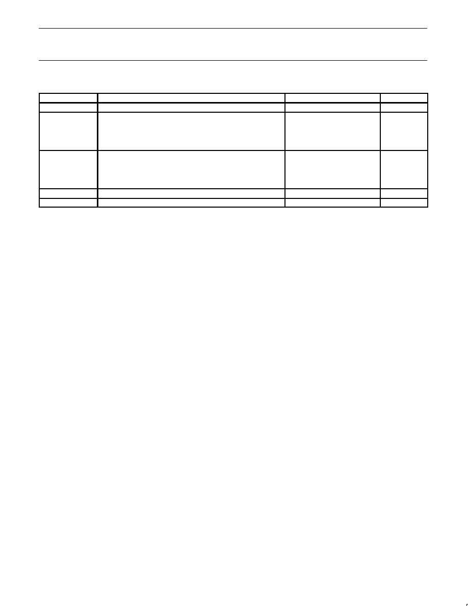
ABSOLUTE MAXIMUM RATINGS
SYMBOL
PARAMETER
RATING
UNIT
V
CC
Supply voltage
±
16
V
P
D MAX
Maximum power dissipation,
T
A
=25
°
C (still air)
1
N package
1212
mW
D package
800
mW
T
A
Operating ambient temperature range
NE5512
0 to +70
°
C
SA5512
-40 to +85
°
C
SE5512
-55 to +125
°
C
T
STG
Storage temperature range
-65 to +150
°
C
T
SOLD
Lead soldering temperature (10sec max)
300
°
C
NOTES:
1. The following derating factors should be applied above 25
°
C
N package at 9.7mW/
°
C
D package at 6.4mW/
°
C

Philips Semiconductors Linear Products
Product specification
NE/SA/SE5512
Dual high-performance operational amplifier
August 31, 1994
80
ELECTRICAL PERFORMANCE CHARACTERISTICS
V
CC
=
±
15V, T
A
= 25
°
C over temperature range, unless otherwise specified.
SYMBOL
PARAMETER
TEST CONDITIONS
SE5512
NE/SA5512
UNIT
SYMBOL
PARAMETER
TEST CONDITIONS
Min
Typ
Max
Min
Typ
Max
UNIT
V
OS
Input offset voltage
R
S
=100
T
A
=+25
°
C
Over temp.
0.7
1
2
3
1
1.5
5
6
mV
V
OS
/
T
4
5
µ
V/
°
C
I
OS
Input offset current
R
S
=100k
T
A
=+25
°
C
Over temp.
3
4
10
20
6
8
20
30
nA
I
OS
/
T
30
40
pA/
°
C
I
BIAS
Input bias current
R
S
=100k
T
A
=+25
°
C
Over temp.
3
4
10
20
6
8
20
30
nA
I
BIAS
/
T
30
40
pA/
°
C
R
IN
Input resistance differential
T
A
=+25
°
C
100
100
M
V
CM
Input common mode range
T
A
=+25
°
C
Over temp.
±
13.5
±
13
±
13.7
±
13.2
±
13.5
±
13
±
13.7
±
13.2
V
CMRR
Input common-mode rejection
ratio
V
CC
=
±
15V
V
IN
=
±
13.5V
CMRR
Input common-mode rejection
ratio
T
A
=+25
°
C
70
100
70
100
dB
ratio
V
IN
=
±
13V
Over temp.
A
V
Large-signal voltage gain
R
L
=2k
T
A
=25
°
C
V
O
=
±
10V over temp.
50
25
200
50
25
200
V/mV
SR
Slew rate
T
A
=25
°
C
0.6
1
1
V/
µ
s
GBW
Small-signal unity gain band-
width
T
A
=25
°
C
3
3
MHz
M
Phase margin
T
A
=25
°
C
45
45
degree
V
OUT
Output voltage swing
R
L
=2k
T
A
=25
°
C
Over temp.
±
13
±
12.5
±
13.5
±
13
±
13
±
12.5
±
13.5
±
13
V
V
OUT
Output voltage swing
R
L
=600
1
T
A
=25
°
C
Over temp.
±
10
±
7.5
±
11.5
±
9
±
10
±
8
±
11.5
±
9
V
I
CC
Power supply current
R
L
=Open
T
A
=25
°
C
Over temp.
3.4
3.6
5
5.5
3.4
3.6
5
5.5
mA
PSRR
Power supply rejection ratio
Over temp.
80
100
80
100
dB
AA
Amplifier-to-amplifier coupling
f=1kHz to 20kHz,
T
A
=25
°
C
-120
-120
dB
THD
Total harmonic distortion
f=10kHz
T
A
=25
°
C
V
O
=7V
RMS
0.01
0.01
%
V
NOISE
Input noise voltage
f=1kHz
T
A
=25
°
C
30
30
nV/
Hz
I
NOISE
Input noise current
f=1kHz
T
A
=25
°
C
0.2
0.2
pA/
Hz
I
SC
Short-circuit current
±
15V, T
A
=25
°
C
40
40
mA
NOTES:
1. Not to exceed maximum package power dissipation.
