
Philips
Semiconductors
MB2245
16-bit transceivers with direction pins
(3-State)
Product specification
Supersedes data of 1993 Aug 18
IC23 Data Handbook
1998 Jan 16
INTEGRATED CIRCUITS
Philips Semiconductors
Product specification
MB2245
16-bit transceiver with direction pins (3-State)
2
1998 Jan 16
8531573 18869
FEATURES
·
16-bit bidirectional bus interface
·
Powerup 3-State
·
Multiple V
CC
and GND pins minimize switching noise
·
3-State buffers
·
Output capability: +64 mA/32mA
·
Latch-up protection exceeds 500mA per Jedec Std 17
·
ESD protection exceeds 2000 V per MIL STD 883 Method 3015
and 200V per Machine Model
·
Inputs are disabled during 3-State mode
DESCRIPTION
The MB2245 high-performance BiCMOS device combines low static
and dynamic power dissipation with high speed and high output
drive.
The MB2245 device is a 16-bit transceiver featuring non-inverting
3-State bus compatible outputs in both send and receive directions.
The control function implementation minimizes external timing
requirements. The device features two Output Enable (1OE, 2OE)
inputs for easy cascading and two Direction (1DIR, 2DIR) inputs for
direction control.
QUICK REFERENCE DATA
SYMBOL
PARAMETER
CONDITIONS
T
amb
= 25
°
C; GND = 0V
TYPICAL
UNIT
t
PLH
t
PHL
Propagation delay
nAx to nBx or nBx to nAx
C
L
= 50pF; V
CC
= 5V
3.2
3.1
ns
C
IN
Input capacitance
V
I
= 0V or V
CC
4
pF
C
I/O
I/O pin capacitance
V
O
= 0V or V
CC
; 3-State
7
pF
I
CCZ
Total supply current
Outputs disabled; V
CC
= 5.5V
65
µ
A
ORDERING INFORMATION
PACKAGES
TEMPERATURE RANGE
OUTSIDE NORTH AMERICA
NORTH AMERICA
DWG NUMBER
52pin plastic Quad Flat Pack
40
°
C to +85
°
C
MB2245 BB
MB2245 BB
SOT379-1
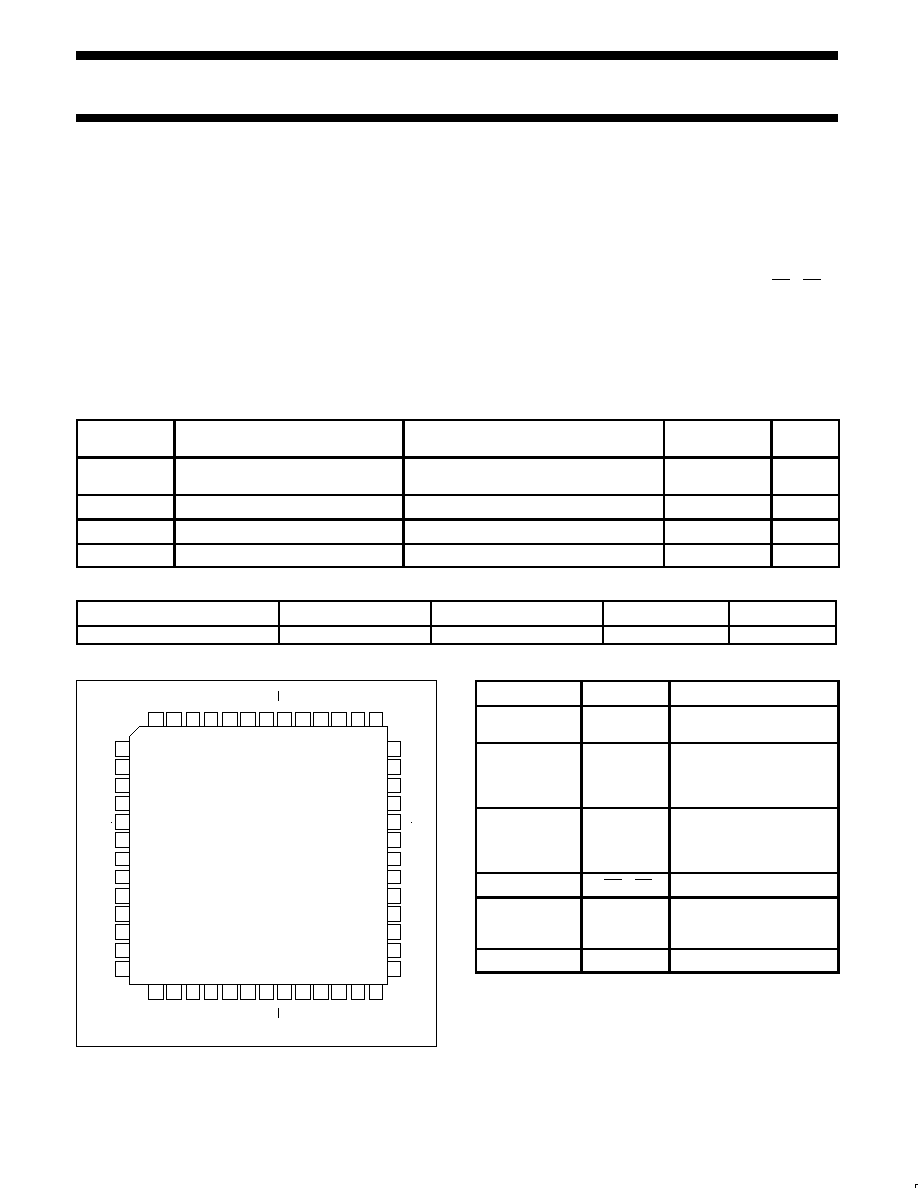
PIN CONFIGURATION
Č
Č
1B3
1B2
GND
1B1
1B0
1DIR
GND
1OE
1A0
1A1
GND
1A2
1A3
2B4
2B5
GND
2B6
2B7
2DIR
GND
2OE
2A7
2A6
GND
2A5
2A4
19
22
20
23
17
16
25
26
24
15
14
21
18
1B7
2B1
GND
GND
GND
1B5
2B3
VCC
2B2
1B4
2B0
1B6
VCC
1
2
3
4
5
6
7
8
9
10
11
12
13
47
44
46
43
49
50
41 40
42
51
52
45
48
1A7
2A1
GND
GND
GND
1A5
2A3
VCC
2A2
1A4
2A0
1A6
VCC
39
38
37
36
35
34
33
32
31
30
29
28
27
52pin PQFP
SB00040
PIN DESCRIPTION
PIN NUMBER
SYMBOL
NAME AND FUNCTION
47, 19
1DIR, 2DIR
Direction control inputs
(Active-High)
44, 43, 41, 40,
38, 37, 35, 34,
32, 31, 29, 28,
26, 25, 23, 22
1A0 1A7,
2A0 2A7
Data inputs/outputs (A side)
48, 49, 51, 52,
2, 3, 5, 6,
8, 9, 11, 12,
14, 15, 17, 18
1B0 1B7,
2B0 2B7
Data outputs/outputs (B side)
45, 21
1OE, 2OE
Output enable (Active-Low)
4, 7, 10, 16, 20,
24, 30, 33, 36,
42, 46, 50
GND
Ground (0V)
1, 13, 27, 39
V
CC
Positive supply voltage
Philips Semiconductors
Product specification
MB2245
16-bit transceiver with direction pins (3-State)
1998 Jan 16
3
LOGIC SYMBOL
2DIR
19
32
31
29
28
26
25
23
22
18
17
15
14
12
11
9
8
2OE
2A0
2A1
2A2
2A3
2A4
2A5
2A6
2A7
2B0
2B1
2B2
2B3
2B4
2B5
2B6
2B7
21
1DIR
47
44
43
41
40
38
37
35
34
6
5
3
2
52
51
49
48
1OE
1A0
1A1
1A2
1A3
1A4
1A5
1A6
1A7
1B0
1B1
1B2
1B3
1B4
1B5
1B6
1B7
45
SB00041
FUNCTION TABLE
INPUTS
INPUTS/OUTPUTS
nOE
nDIR
nAx
nBx
L
L
A = B
Inputs
L
H
Inputs
B = A
H
X
Z
Z
LOGIC SYMBOL (IEEE/IEC)
1
45
44
43
G3
47
3 EN1 (BA)
3 EN2 (AB)
2
48
49
41
51
40
52
38
2
37
3
35
5
34
6
SB00042
1
21
32
31
G3
19
3 EN1 (BA)
3 EN2 (AB)
2
8
9
29
11
28
12
26
14
25
15
23
17
22
18
SB00043
Philips Semiconductors
Product specification
MB2245
16-bit transceiver with direction pins (3-State)
1998 Jan 16
4
ABSOLUTE MAXIMUM RATINGS
1, 2
SYMBOL
PARAMETER
CONDITIONS
RATING
UNIT
V
CC
DC supply voltage
0.5 to +7.0
V
I
IK
DC input diode current
V
I
< 0
18
mA
V
I
DC input voltage
3
1.2 to +7.0
V
I
OK
DC output diode current
V
O
< 0
50
mA
V
OUT
DC output voltage
3
output in Off or High state
0.5 to +5.5
V
I
OUT
DC output current
output in Low state
128
mA
T
stg
Storage temperature range
65 to 150
°
C
NOTES:
1. Stresses beyond those listed may cause permanent damage to the device. These are stress ratings only and functional operation of the
device at these or any other conditions beyond those indicated under "recommended operating conditions" is not implied. Exposure to
absolute-maximum-rated conditions for extended periods may affect device reliability.
2. The performance capability of a high-performance integrated circuit in conjunction with its thermal environment can create junction
temperatures which are detrimental to reliability. The maximum junction temperature of this integrated circuit should not exceed 150
°
C.
3. The input and output voltage ratings may be exceeded if the input and output current ratings are observed.
RECOMMENDED OPERATING CONDITIONS
SYMBOL
PARAMETER
LIMITS
UNIT
Min
Max
V
CC
DC supply voltage
4.5
5.5
V
V
I
Input voltage
0
V
CC
V
V
IH
High-level input voltage
2.0
V
V
IL
Low-level Input voltage
0.8
V
I
OH
High-level output current
32
mA
I
OL
Low-level output current
64
mA
t/
v
Input transition rise or fall rate
0
10
ns/V
T
amb
Operating free-air temperature range
40
+85
°
C
Philips Semiconductors
Product specification
MB2245
16-bit transceiver with direction pins (3-State)
1998 Jan 16
5
DC ELECTRICAL CHARACTERISTICS
LIMITS
SYMBOL
PARAMETER
TEST CONDITIONS
T
amb
= +25
°
C
T
amb
= 40
°
C
to +85
°
C
UNIT
Min
Typ
Max
Min
Max
V
IK
Input clamp voltage
V
CC
= 4.5V; I
IK
= 18mA
0.9
1.2
1.2
V
V
CC
= 4.5V; I
OH
= 3mA; V
I
= V
IL
or V
IH
2.5
2.9
2.5
V
V
OH
High-level output voltage
V
CC
= 5.0V; I
OH
= 3mA; V
I
= V
IL
or V
IH
3.0
3.4
3.0
V
V
CC
= 4.5V; I
OH
= 32mA; V
I
= V
IL
or V
IH
2.0
2.4
2.0
V
V
OL
Low-level output voltage
V
CC
= 4.5V; I
OL
= 64mA; V
I
= V
IL
or V
IH
0.42
0.55
0.55
V
I
I
Input leakage current
V
CC
= 5.5V; V
I
= GND or 5.5V
±
0.01
±
1.0
±
1.0
µ
A
I
OFF
Power-off leakage current
V
CC
= 0.0V; V
O
or V
I
4.5V
±
5.0
±
100
±
100
µ
A
I
PU
/I
PU
Power-up/down 3-State
output current
V
CC
= 2.0V; V
O
= 0.5V; V
I
= GND or V
CC;
V
OE
= V
CC
±
5.0
±
50
±
50
µ
A
I
OZH
3-State output High current
V
CC
= 5.5V; V
O
= 2.7V; V
I
= V
IL
or V
IH
5.0
50
50
µ
A
I
OZL
3-State output Low current
V
CC
= 5.5V; V
O
= 0.5V; V
I
= V
IL
or V
IH
5.0
50
50
µ
A
I
CEX
Output high leakage current
V
CC
= 5.5V; V
O
= 5.5V; V
I
= GND or V
CC
5.0
50
50
µ
A
I
O
Output current
1
V
CC
= 5.5V; V
O
= 2.5V
50
70
180
50
180
mA
I
CCH
V
CC
= 5.5V; Outputs High, V
I
= GND or V
CC
65
250
250
µ
A
I
CCL
Quiescent supply current
V
CC
= 5.5V; Outputs Low, V
I
= GND or V
CC
48
60
60
mA
I
CCZ
V
CC
= 5.5V; Outputs 3-State;
V
I
= GND or V
CC
65
250
250
µ
A
I
CC
Additional supply current per
input pin
2
Outputs enabled, one input at 3.4V, other
inputs at V
CC
or GND; V
CC
= 5.5V
0.5
1.5
1.5
mA
NOTES:
1. Not more than one output should be tested at a time, and the duration of the test should not exceed one second.
2. This is the increase in supply current for each input at 3.4V.
AC CHARACTERISTICS
GND = 0V; t
R
= t
F
= 2.5ns; C
L
= 50pF, R
L
= 500
LIMITS
SYMBOL
PARAMETER
WAVEFORM
T
amb
= +25
°
C
V
CC
= +5.0V
T
amb
= 40
°
C to +85
°
C
V
CC
= +5.0V
±
0.5V
UNIT
Min
Typ
Max
Min
Max
t
PLH
t
PHL
Propagation delay
nAx to nBx or nBx to nAx
1
1.2
1.2
3.2
3.1
4.5
4.5
1.2
1.2
5.1
5.1
ns
t
PZH
t
PZL
Output enable time
to High and Low level
2
2.1
2.4
3.8
4.7
5.2
6.1
2.1
2.4
5.8
7.1
ns
t
PHZ
t
PLZ
Output disable time
from High and Low level
2
2.1
2.1
4.5
4.0
5.8
5.3
2.1
2.1
6.4
5.9
ns