Äîêóìåíòàöèÿ è îïèñàíèÿ www.docs.chipfind.ru

ISP1583
Hi-Speed Universal Serial Bus peripheral controller
Rev. 03 -- 12 July 2004
Product data
1.
General description
The ISP1583 is a cost-optimized and feature-optimized Hi-Speed Universal Serial
Bus (USB) peripheral controller. It fully complies with
Universal Serial Bus
Specification Rev. 2.0, supporting data transfer at high-speed (480 Mbit/s) and
full-speed (12 Mbit/s).
The ISP1583 provides high-speed USB communication capacity to systems based
on microcontrollers or microprocessors. It communicates with a microcontroller or
microprocessor of a system through a high-speed general-purpose parallel interface.
The ISP1583 supports automatic detection of Hi-Speed USB system operation.
Original USB fall-back mode allows the device to remain operational under full-speed
conditions. It is designed as a generic USB peripheral controller so that it can fit into
all existing device classes, such as imaging class, mass storage devices,
communication devices, printing devices and human interface devices.
The ISP1583 is a low-voltage device, which supports I/O pad voltages from 1.65 V to
3.6 V.
The internal generic Direct Memory Access (DMA) block allows easy integration into
data streaming applications. In addition, the various configurations of the DMA block
are tailored for mass storage applications.
The modular approach to implementing a USB peripheral controller allows the
designer to select the optimum system microcontroller from the wide variety available.
The ability to reuse existing architecture and firmware investments shortens the
development time, eliminates risk and reduces cost. The result is fast and efficient
development of the most cost-effective USB peripheral solution.
The ISP1583 is ideally suited for many types of peripherals, such as: printers;
scanners; magneto-optical, compact disc, digital video disc and Zip
®
drives; digital
still cameras; USB-to-Ethernet links; cable and DSL modems. The low power
consumption during suspend mode allows easy design of equipment that is compliant
to the ACPITM, OnNowTM and USB power management requirements.
The ISP1583 also incorporates features such as SoftConnectTM, a reduced
frequency crystal oscillator, and integrated termination resistors. These features allow
significant cost savings in system design and easy implementation of advanced USB
functionality into PC peripherals.

Philips Semiconductors
ISP1583
Hi-Speed USB peripheral controller
Product data
Rev. 03 -- 12 July 2004
2 of 87
9397 750 13461
© Koninklijke Philips Electronics N.V. 2004. All rights reserved.
2.
Features
s
Complies fully with:
x
Universal Serial Bus Specification Rev. 2.0
x
Most Device Class specifications
x
ACPITM, OnNowTM and USB power management requirements
s
Supports data transfer at high-speed (480 Mbit/s) and full-speed (12 Mbit/s)
s
Direct interface to ATA/ATAPI peripherals; applicable only in split bus mode
s
High performance USB peripheral controller with integrated Serial Interface
Engine (SIE), Parallel Interface Engine (PIE), FIFO memory and data transceiver
s
Automatic Hi-Speed USB mode detection and Original USB fall-back mode
s
Supports sharing mode
s
Supports I/O voltage range of 1.65 V to 3.6 V
s
Supports V
BUS
sensing
s
High-speed DMA interface
s
Configurable direct access data path from the microprocessor to an ATA device
s
Fully autonomous and multi configuration DMA operation
s
7 IN endpoints, 7 OUT endpoints and a fixed control IN/OUT endpoint
s
Integrated physical 8 kbytes of multi configuration FIFO memory
s
Endpoints with double buffering to increase throughput and ease real-time data
transfer
s
Bus-independent interface with most microcontrollers and microprocessors
s
12 MHz crystal oscillator with integrated PLL for low EMI
s
Software-controlled connection to the USB bus (SoftConnectTM)
s
Low-power consumption in operation and power-down modes; suitable for use in
bus-powered USB devices
s
Supports Session Request Protocol (SRP) that complies with
On-The-Go
Supplement to the USB Specification Rev. 1.0a
s
Internal power-on and low-voltage reset circuits; also supports software reset
s
Operation over the extended USB bus voltage range (DP, DM and V
BUS
)
s
5 V tolerant I/O pads at 3.3 V
s
Operating temperature range from
-
40
°
C to +85
°
C
s
Available in HVQFN64 halogen-free and lead-free package.
3.
Applications
s
Personal digital assistant
s
Mass storage device, for example: Zip, Magneto-Optical (MO), CD and DVD
drives
s
Digital video camera
s
Digital still camera
s
3G mobile phone
s
MP3 player
s
Communication device, for example: router and modem
s
Printer

Philips Semiconductors
ISP1583
Hi-Speed USB peripheral controller
Product data
Rev. 03 -- 12 July 2004
3 of 87
9397 750 13461
© Koninklijke Philips Electronics N.V. 2004. All rights reserved.
s
Scanner.
4.
Abbreviations
DMA -- Direct Memory Access
EMI -- ElectroMagnetic Interference
FS -- Full-speed
GDMA -- Generic DMA
HS -- High-speed
MDMA -- Multiword DMA
MMU -- Memory Management Unit
MO -- Magneto-Optical
NRZI -- Non-Return-to-Zero Inverted
OTG -- On-The-Go
PDA -- Personal Digital Assistant
PID -- Packet IDentifier
PIE -- Parallel Interface Engine
PIO -- Parallel Input/Output
PLL -- Phase-Locked Loop
SE0 -- Single-Ended zero
SIE -- Serial Interface Engine
SRP -- Session Request Protocol
USB -- Universal Serial Bus.
5.
Ordering information
Table 1:
Ordering information
Type
number
Package
Name
Description
Version
ISP1583BS
HVQFN64
plastic thermal enhanced very thin quad flat package;
no leads; 64 terminals; body 9
×
9
×
0.85 mm
SOT804-1
xxxx xxxxxxxxxxxxxxxxxxxxxxxxxxxxxx x xxxxxxxxxxxxxx xxxxxxxxxx xxx xxxxxx xxxxxxxxxxxxxxxxxxxxxxx xxxxxxxxxxxxxxxxxxxxxx
xxxxx xxxxxx xx xxxxxxxxxxxxxxxxxxxxxxxxxxxxx xxxxxxxxxxxxxxxxxxxxxx xxxxxxxxxxx xxxxxxx xxxxxxxxxxxxxxxxxxx
xxxxxxxxxxxxxxxx xxxxxxxxxxxxxx xxxxxx xx xxxxxxxxxxxxxxxxxxxxxxxxxxxxxxxx xxxxxxxxxxxxxxxxxxxxxxxx xxxxxxx
xxxxxxxxxxxxxxxxxxxxxxxxxxxxxxxxxxxxxxxxxxxxxx xxxxxxxxxxx xxxxx x x
Philips Semiconductor
s
ISP1583
Hi-Speed USB peripheral contr
oller
9397 750 13461
© K
oninklijk
e Philips Electronics N.V
. 2004. All r
ights reser
v
ed.
Pr
oduct data
Re
v
.
03 -- 12 J
u
l
y
2004
4 of 87
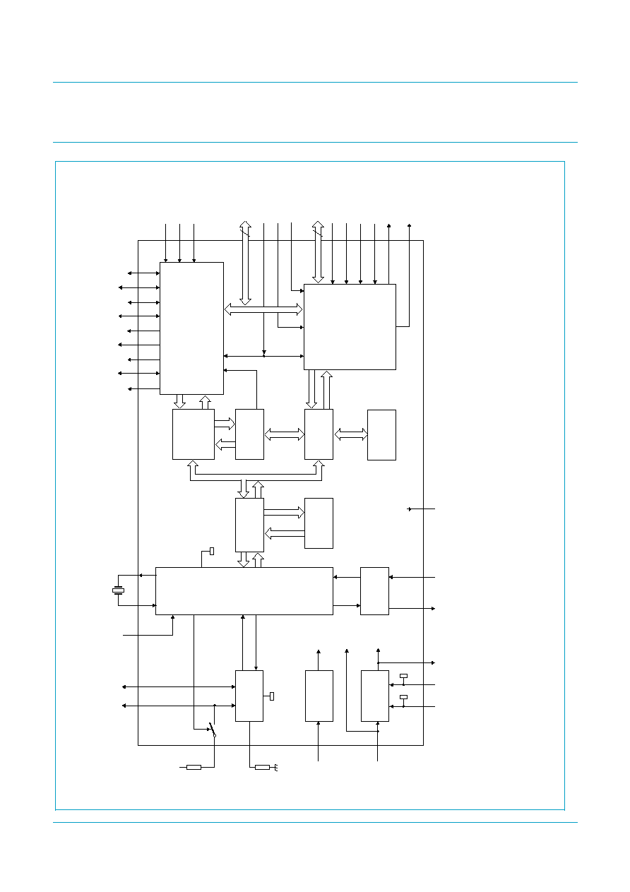
6.
Bloc
k dia
gram
The direction of pins DREQ, DACK, DIOR and DIOW is determined by bit MASTER (DMA Hardware register) and bit ATA_MODE (DMA Configuration register).
(1) Pin 15 is shared by READY and IORDY.
(2) Pin 60 is shared by MODE0 and DA1.
(3) Pin 62 is shared by BUS_CONF and DA0.
Fig 1.
Block diagram.
004aaa268
1.5 k
12.0 k
ISP1583
HI-SPEED USB
TRANSCEIVER
RESET_N
RREF
VOLTAGE
REGULATORS
POWER-ON
RESET
MEMORY
MANAGEMENT
UNIT
INTEGRATED
RAM
(8 KBYTES)
MICROCONTROLLER
INTERFACE
DMA INTERFACE
MICRO-
CONTROLLER
HANDLER
DMA
HANDLER
DMA
REGISTERS
12 MHz
XTAL2
XTAL1
to/from USB
SYSTEM
CONTROLLER
PHILIPS
SIE/PIE
SoftConnect
INT
internal
reset
DATA[15:0]
MODE0
(2)
BUS_CONF
(3)
8
AD[7:0]
DREQ
CS0_N
V
CC(3V3)
digital
supply
1.8 V
INTRQ
IORDY
(1)
RPU
DM
DP
V
CC(1V8)
SUSPEND WAKEUP
AGND
DGND
CS_N
EOT
V
CC(I/O)
V
BUS
16
OTG SRP
MODULE
analog
supply
1, 5
2
3
4
6
7
8
DACK
DIOR
DIOW
CS1_N
DA0
(3)
DA1
(2)
DA2
9
10
11
12
21
13, 35,59
ALE/A0
RW_N/RD_N
DS_N/WR_N
14
15
17
18
READY
(1)
19
20
22
23 to 25,
27 to 31
26, 41, 54
32, 56
60
36
37 to 40,
42 to 53
55
58
57
60
61
15
16
62
62
63
64
MODE1
34
I/O pad supply
3.3 V
Philips Semiconductors
ISP1583
Hi-Speed USB peripheral controller
Product data
Rev. 03 -- 12 July 2004
5 of 87
9397 750 13461
© Koninklijke Philips Electronics N.V. 2004. All rights reserved.
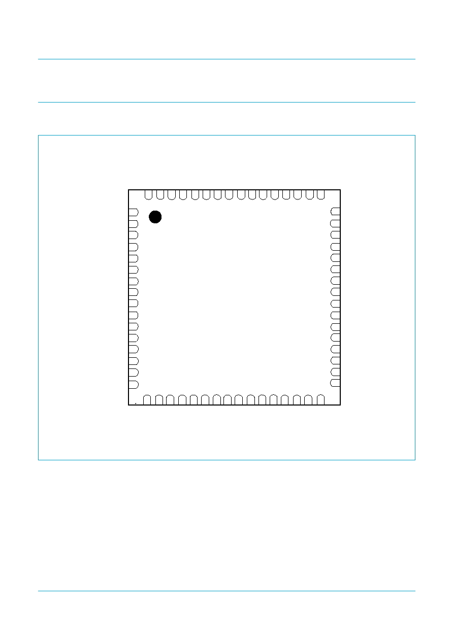
7.
Pinning information
7.1 Pinning
Fig 2.
Pin configuration HVQFN64 (top view).
004aaa537
MODE1
DGND
ALE/A0
DATA8
DATA1
DATA2
DATA3
V
CC(I/O)
DATA4
DATA5
DATA6
DATA7
DATA13
DATA14
READY/IORDY
INTRQ
DGND
DIOW
DIOR
DREQ
DACK
RESET_N
RREF
EOT
DM
DP
CS_N
DS_N/WR_N
RW_N/RD_N
CS0_N
CS1_N
AD0
AD1
AD2
V
CC(I/O)
AD3
AD4
AD5
AD6
AD7
WAKEUP
DATA15
V
CC(1V8)
V
BUS
4
5
6
2
3
10
11
12
7
8
9
14
15
13
45
44
43
47
46
39
38
37
42
41
40
35
34
36
51
52
53
49
50
57
58
59
54
55
56
61
62
60
18
19
20
21
22
23
24
25
26
27
28
29
30
31
ISP1583BS
AGND
XTAL1
XTAL2
DATA12
V
CC(I/O)
DATA0
BUS_CONF/DA0
V
CC(3V3)
INT
16
AGND
1
DATA11
63
64
SUSPEND
48
DATA9
DATA10
33
n.c.
V
CC(1V8)
32
DA2
17
RPU
MODE0/DA1
DGND
Philips Semiconductors
ISP1583
Hi-Speed USB peripheral controller
Product data
Rev. 03 -- 12 July 2004
6 of 87
9397 750 13461
© Koninklijke Philips Electronics N.V. 2004. All rights reserved.
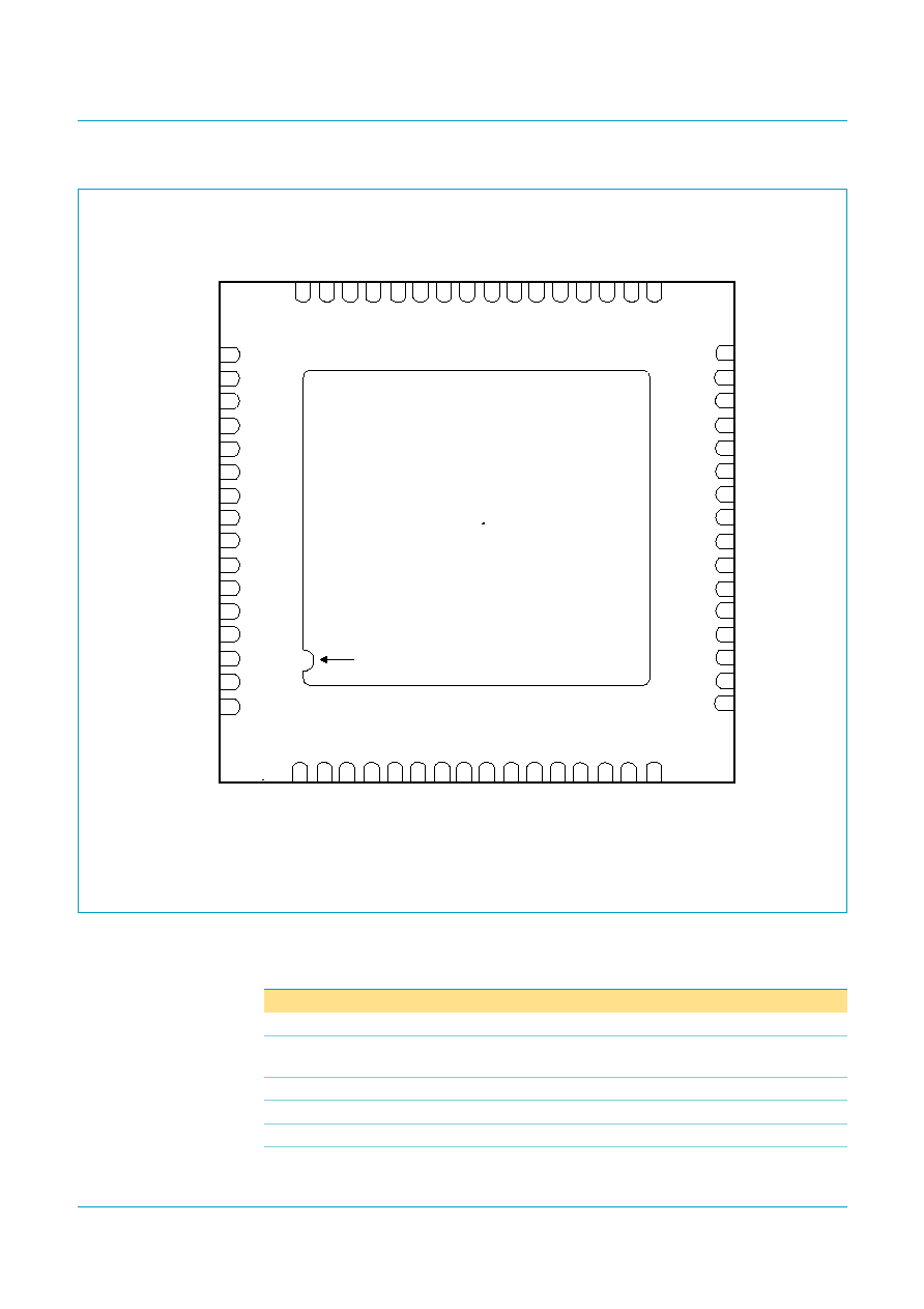
7.2 Pin description
Fig 3.
Pin configuration HVQFN64 (bottom view).
004aaa376
DATA9
DATA8
DATA7
DGND
DATA5
DATA4
V
CC(I/O)
DATA3
DATA2
DATA1
DATA0
ALE/A0
AD6
AD5
RPU
DP
DM
AGND
RREF
EOT
RESET_N
DACK
DIOR
DREQ
DGND
INTRQ
WAKEUP
V
CC(3V3)
BUS_CONF/DA0
MODE0/DA1
DGND
XTAL1
XTAL2
V
CC(1V8)
V
BUS
V
CC(I/O)
DATA15
DATA14
DATA13
DATA12
CS_N
AD4
AD2
V
CC(I/O)
13
12
11
15
14
7
6
5
10
9
8
3
2
4
36
37
38
34
35
42
43
44
39
40
41
46
47
45
30
29
28
32
31
24
23
22
27
26
25
20
19
21
63
62
61
60
59
58
57
56
55
54
53
52
51
50
ISP1583BS
DIOW
AD0
AD1
AD7
AD3
DATA6
RW_N/RD_N
DS_N/
WR_N
AGND
1
INT
16
V
CC(1V8)
18
17
DA2
33
MODE1
n.c.
48
DATA10
DATA11
49
SUSPEND
64
READY/IORDY
CS0_N
CS1_N
GND (exposed die pad)
Bottom view
terminal 1
Table 2:
Pin description
Symbol
[1]
Pin
Type
[2]
Description
AGND
1
-
analog ground
RPU
2
A
pull-up resistor connection; this pin must be connected to 3.3 V
through an external 1.5 k
resistor for pulling-up pin DP
DP
3
A
USB D+ line connection (analog)
DM
4
A
USB D
-
line connection (analog)
AGND
5
-
analog ground
RREF
6
A
external bias resistor connection; this pin must be connected to
ground via a 12.0 k
±
1 % resistor

Philips Semiconductors
ISP1583
Hi-Speed USB peripheral controller
Product data
Rev. 03 -- 12 July 2004
7 of 87
9397 750 13461
© Koninklijke Philips Electronics N.V. 2004. All rights reserved.
RESET_N
7
I
reset input (500
µ
s); a LOW level produces an asynchronous
reset; connect to V
CC(3V3)
for power-on reset (internal POR
circuit)
TTL; 5 V tolerant
[6]
EOT
8
I
end-of-transfer input (programmable polarity); used in DMA
slave mode only; when not in use, connect this pin to V
CC(I/O)
through a 10 k
resistor
input pad; TTL; 5 V tolerant
[6]
DREQ
9
I/O
DMA request input or output (programmable polarity); the
signal direction depends on bit MASTER in register DMA
Hardware (see
Table 57
):
·
Input: DMA master if bit MASTER = 1
·
Output: DMA slave if bit MASTER = 0.
When not in use, in the default setting, this pin must be
connected to ground through a 10 k
resistor.
bidirectional pad; 4 ns slew-rate control; TTL; 5 V tolerant
[6]
DACK
10
I/O
DMA acknowledge input or output (programmable polarity); the
signal direction depends on bit MASTER in register DMA
Hardware (see
Table 57
):
·
Input: DMA slave if bit MASTER = 0
·
Output: DMA master if bit MASTER = 1.
When not in use, in the default setting, this pin must be
connected to V
CC(I/O)
through a 10 k
resistor.
bidirectional pad; 4 ns slew-rate control; TTL; 5 V tolerant
[6]
DIOR
11
I/O
DMA read strobe input or output (programmable polarity); the
signal direction depends on bit MASTER in register DMA
Hardware (see
Table 57
):
·
Input: DMA slave if bit MASTER = 0
·
Output: DMA master if bit MASTER = 1.
When not in use, in the default setting, this pin must be
connected to V
CC(I/O)
through a 10 k
resistor.
bidirectional pad; 4 ns slew-rate control; TTL; 5 V tolerant
[6]
DIOW
12
I/O
DMA write strobe input or output (programmable polarity); the
signal direction depends on bit MASTER in register DMA
Hardware (see
Table 57
):
·
Input: DMA slave if bit MASTER = 0
·
Output: DMA master if bit MASTER = 1.
When not in use, in the default setting, this pin must be
connected to V
CC(I/O)
through a 10 k
resistor.
bidirectional pad; 4 ns slew-rate control; TTL; 5 V tolerant
[6]
DGND
13
-
digital ground
INTRQ
14
I
interrupt request input; from the ATA/ATAPI peripheral; use a
10 k
resistor to pull-down
input pad; TTL; 5 V tolerant
[6]
Table 2:
Pin description
...continued
Symbol
[1]
Pin
Type
[2]
Description

Philips Semiconductors
ISP1583
Hi-Speed USB peripheral controller
Product data
Rev. 03 -- 12 July 2004
8 of 87
9397 750 13461
© Koninklijke Philips Electronics N.V. 2004. All rights reserved.
READY/
IORDY
15
I/O
Signal ready output -- Used in generic processor mode:
·
LOW: the ISP1583 is processing a previous command or
data and is not ready for the next command or data transfer
·
HIGH: the ISP1583 is ready for the next microprocessor
read or write.
DMA ready input -- Used in split bus mode for accessing
ATA/ATAPI peripherals (PIO mode only).
bidirectional pad; 10 ns slew-rate control; TTL; 5 V tolerant
[6]
INT
16
O
interrupt output; programmable polarity (active HIGH or LOW)
and signaling (edge or level triggered)
CMOS output; 8 mA drive
DA2
[5]
17
O
address output to select the Task File register of an ATA/ATAPI
device; see
Table 59
CMOS output; 8 mA drive
CS_N
18
I
chip selection input
input pad; TTL; 5 V tolerant
[6]
RW_N/
RD_N
19
I
Read and write input -- For Motorola style, this function is
determined by pin MODE0 = LOW during power-up.
Read input -- For 8051 style, this function is determined by
pin MODE0 = HIGH during power-up.
input pad; TTL; 5 V tolerant
[6]
DS_N/
WR_N
20
I
Data selection input -- For Motorola style, this function is
determined by pin MODE0 = LOW at power-up.
Write input -- For 8051 style, this function is determined by
pin MODE0 = HIGH at power-up.
input pad; TTL; 5 V tolerant
[6]
CS0_N
[5]
21
O
chip selection output 0 for ATA/ATAPI device; see
Table 59
CMOS output; 8 mA drive
CS1_N
[5]
22
O
chip selection output 1 for ATA/ATAPI device; see
Table 59
CMOS output; 8 mA drive
AD0
23
I/O
bit 0 of multiplexed address and data
bidirectional pad; 4 ns slew-rate control; TTL; 5 V tolerant
[6]
AD1
24
I/O
bit 1 of multiplexed address and data bus
bidirectional pad; 4 ns slew-rate control; TTL; 5 V tolerant
[6]
AD2
25
I/O
bit 2 of multiplexed address and data bus
bidirectional pad; 4 ns slew-rate control; TTL; 5 V tolerant
[6]
V
CC(I/O)
[3]
26
-
I/O pad supply voltage (1.65 V to 3.6 V); see
Section 8.15
AD3
27
I/O
bit 3 of multiplexed address and data bus
bidirectional pad; 4 ns slew-rate control; TTL; 5 V tolerant
[6]
AD4
28
I/O
bit 4 of multiplexed address and data bus
bidirectional pad; 4 ns slew-rate control; TTL; 5 V tolerant
[6]
AD5
29
I/O
bit 5 of multiplexed address and data bus
bidirectional pad; 4 ns slew-rate control; TTL; 5 V tolerant
[6]
Table 2:
Pin description
...continued
Symbol
[1]
Pin
Type
[2]
Description

Philips Semiconductors
ISP1583
Hi-Speed USB peripheral controller
Product data
Rev. 03 -- 12 July 2004
9 of 87
9397 750 13461
© Koninklijke Philips Electronics N.V. 2004. All rights reserved.
AD6
30
I/O
bit 6 of multiplexed address and data bus
bidirectional pad; 4 ns slew-rate control; TTL; 5 V tolerant
[6]
AD7
31
I/O
bit 7 of multiplexed address and data bus
bidirectional pad; 4 ns slew-rate control; TTL; 5 V tolerant
[6]
V
CC(1V8)
[3]
32
-
voltage regulator output (1.8 V
±
0.15 V); tapped out voltage
from the internal regulator; this regulated voltage cannot drive
external devices; decouple this pin using a 0.1
µ
F capacitor;
see
Section 8.15
n.c.
33
-
not connected
MODE1
34
I
mode selection input 1; used in split bus mode only:
·
LOW: ALE function (address latch enable)
·
HIGH: A0 function (address/data indicator).
Remark: When operating in generic processor mode, set pin
MODE1 HIGH.
input pad; TTL; 5 V tolerant
[6]
DGND
35
-
digital ground
ALE/A0
36
I
Address latch enable input -- When pin MODE1 = LOW
during power-up, a falling edge latches the address on the
multiplexed address and data bus AD[7:0].
Address and data selection input -- When pin
MODE1 = HIGH during power-up, the function is determined
by the level on this pin (detected on the rising edge of the
WR_N pulse):
·
HIGH: bus AD[7:0] is a register address
·
LOW: bus AD[7:0] is register data; used in split bus mode
only.
Remark: When operating in generic processor mode with pin
MODE1 = HIGH, this pin must be pulled down using a 10 k
resistor.
input pad; TTL; 5 V tolerant
[6]
DATA0
37
I/O
bit 0 of bidirectional data bus
bidirectional pad; 4 ns slew-rate control; TTL; 5 V tolerant
[6]
DATA1
38
I/O
bit 1 of bidirectional data bus
bidirectional pad; 4 ns slew-rate control; TTL; 5 V tolerant
[6]
DATA2
39
I/O
bit 2 of bidirectional data bus
bidirectional pad; 4 ns slew-rate control; TTL; 5 V tolerant
[6]
DATA3
40
I/O
bit 3 of bidirectional data bus
bidirectional pad; 4 ns slew-rate control; TTL; 5 V tolerant
[6]
V
CC(I/O)
[3]
41
-
I/O pad supply voltage (1.65 V to 3.6 V); see
Section 8.15
DATA4
42
I/O
bit 4 of bidirectional data bus
bidirectional pad; 4 ns slew-rate control; TTL; 5 V tolerant
[6]
DATA5
43
I/O
bit 5 of bidirectional data bus
bidirectional pad; 4 ns slew-rate control; TTL; 5 V tolerant
[6]
Table 2:
Pin description
...continued
Symbol
[1]
Pin
Type
[2]
Description

Philips Semiconductors
ISP1583
Hi-Speed USB peripheral controller
Product data
Rev. 03 -- 12 July 2004
10 of 87
9397 750 13461
© Koninklijke Philips Electronics N.V. 2004. All rights reserved.
DATA6
44
I/O
bit 6 of bidirectional data bus
bidirectional pad; 4 ns slew-rate control; TTL; 5 V tolerant
[6]
DATA7
45
I/O
bit 7 of bidirectional data bus
bidirectional pad; 4 ns slew-rate control; TTL; 5 V tolerant
[6]
DATA8
46
I/O
bit 8 of bidirectional data bus
bidirectional pad; 4 ns slew-rate control; TTL; 5 V tolerant
[6]
DATA9
47
I/O
bit 9 of bidirectional data bus
bidirectional pad; 4 ns slew-rate control; TTL; 5 V tolerant
[6]
DATA10
48
I/O
bit 10 of bidirectional data bus
bidirectional pad; 4 ns slew-rate control; TTL; 5 V tolerant
[6]
DATA11
49
I/O
bit 11 of bidirectional data bus
bidirectional pad; 4 ns slew-rate control; TTL; 5 V tolerant
[6]
DATA12
50
I/O
bit 12 of bidirectional data bus
bidirectional pad; 4 ns slew-rate control; TTL; 5 V tolerant
[6]
DATA13
51
I/O
bit 13 of bidirectional data bus
bidirectional pad; 4 ns slew-rate control; TTL; 5 V tolerant
[6]
DATA14
52
I/O
bit 14 of bidirectional data bus
bidirectional pad; 4 ns slew-rate control; TTL; 5 V tolerant
[6]
DATA15
53
I/O
bit 15 of bidirectional data bus
bidirectional pad; 4 ns slew-rate control; TTL; 5 V tolerant
[6]
V
CC(I/O)
[3]
54
-
I/O pad supply voltage (1.65 V to 3.6 V); see
Section 8.15
V
BUS
55
A
USB bus power sensing input -- Used to detect whether the
host is connected or not; when V
BUS
is not detected, pin RPU
is internally disconnected from pin DP in approximately 4 ns
V
BUS
pulsing output -- In OTG mode.
Connect a 1
µ
F electrolytic capacitor and a 1 M
pull-down
resistor to ground; see
Section 8.13
5 V tolerant
[6]
V
CC(1V8)
[3]
56
-
voltage regulator output (1.8 V
±
0.15 V); tapped out voltage
from the internal regulator; this regulated voltage cannot drive
external devices; decouple this pin using 4.7
µ
F and 0.1
µ
F
capacitors; see
Section 8.15
XTAL2
57
O
crystal oscillator output (12 MHz); connect a fundamental
parallel-resonant crystal; leave this pin open when using an
external clock source on pin XTAL1; see
Table 99
XTAL1
58
I
crystal oscillator input (12 MHz); connect a fundamental
parallel-resonant crystal or an external clock source (leaving
pin XTAL2 unconnected); see
Table 99
DGND
59
-
digital ground
Table 2:
Pin description
...continued
Symbol
[1]
Pin
Type
[2]
Description

Philips Semiconductors
ISP1583
Hi-Speed USB peripheral controller
Product data
Rev. 03 -- 12 July 2004
11 of 87
9397 750 13461
© Koninklijke Philips Electronics N.V. 2004. All rights reserved.
[1]
Symbol names ending with underscore N (for example, NAME_N) represent active LOW signals.
[2]
All outputs and I/O pins can source 4 mA.
[3]
Add a decoupling capacitor (0.1
µ
F) to all the supply pins. For better EMI results, add a 0.01
µ
F
capacitor in parallel to the 0.1
µ
F.
[4]
The DMA bus is in 3-state until a DMA command (see
Section 9.4.1
) is executed.
[5]
The control signals are not 3-state.
[6]
5 V tolerant when V
CC(I/O)
= 3.3 V.
MODE0/
DA1
[5]
60
I/O
Mode selection input 0 -- Selects the read/write strobe
functionality in generic processor mode during power-up:
·
LOW: for Motorola style; the function of pin 19 is RW_N and
pin 20 is DS_N
·
HIGH: for 8051 style; the function of pin 19 is RD_N and
pin 20 is WR_N.
Address selection output -- Selects the Task File register of
an ATA/ATAPI device during normal operation; see
Table 59
bidirectional pad; 10 ns slew-rate control; TTL; 5 V tolerant
[6]
V
CC(3V3)
[3]
61
-
regulator supply voltage (3.3 V
±
0.3 V); this pin supplies the
internal regulator; see
Section 8.15
BUS_CONF/
DA0
[5]
62
I/O
Bus configuration input -- Selects bus mode during
power-up at:
·
LOW: split bus mode; multiplexed 8-bit address and data
bus on AD[7:0], separate DMA data bus on DATA[15:0]
[4]
·
HIGH: generic processor mode; separate 8-bit address on
AD[7:0], 16-bit processor data bus on DATA[15:0]. DMA is
multiplexed on the processor bus as DATA[15:0].
Address selection output -- Selects the Task File register of
an ATA/ATAPI device at normal operation; see
Table 59
bidirectional pad; 10 ns slew-rate control; TTL; 5 V tolerant
[6]
WAKEUP
63
I
wake-up input; when this pin is at the HIGH level, the chip is
prevented from getting into the suspend state and the chip
wakes up from the suspend state; when not in use, connect
this pin to ground through a 10 k
resistor
input pad; TTL; 5 V tolerant
[6]
SUSPEND
64
O
suspend state indicator output; used as a power switch control
output for powered-off application or as a resume signal to the
CPU for powered-on application
CMOS output; 8 mA drive
GND
exposed die
pad
ground supply; down bonded to the exposed die pad
(heatsink); to be connected to the DGND during PCB layout
Table 2:
Pin description
...continued
Symbol
[1]
Pin
Type
[2]
Description

Philips Semiconductors
ISP1583
Hi-Speed USB peripheral controller
Product data
Rev. 03 -- 12 July 2004
12 of 87
9397 750 13461
© Koninklijke Philips Electronics N.V. 2004. All rights reserved.
8.
Functional description
The ISP1583 is a high-speed USB peripheral controller. It implements the Hi-Speed
USB or the Original USB physical layer and the packet protocol layer. It maintains up
to 16 USB endpoints concurrently (control IN and control OUT, 7 IN and 7 OUT
configurable) along with endpoint EP0 setup, which accesses the setup buffer. The
USB Chapter 9 protocol handling is executed by means of external firmware.
The ISP1583 has a fast general-purpose interface for communication with most types
of microcontrollers and microprocessors. This microcontroller interface is configured
by pins BUS_CONF, MODE1 and MODE0 to accommodate most interface types. Two
bus configurations are available, selected via input BUS_CONF during power-up:
·
Generic processor mode (pin BUS_CONF = HIGH):
AD[7:0]: 8-bit address bus (selects target register)
DATA[15:0]: 16-bit data bus (shared by processor and DMA)
Control signals: RW_N and DS_N or RD_N and WR_N (selected via pin
MODE0), CS_N
DMA interface (generic slave mode only): Uses lines DATA[15:0] as data bus,
DIOR and DIOW as dedicated read and write strobes.
·
Split bus mode (pin BUS_CONF = LOW):
AD[7:0]: 8-bit local microprocessor bus (multiplexed address and data)
DATA[15:0]: 16-bit DMA data bus
Control signals: CS_N, ALE or A0 (selected via pin MODE1), RW_N and DS_N
or RD_N and WR_N (selected via pin MODE0)
DMA interface (master or slave mode): Uses DIOR and DIOW as dedicated
read and write strobes.
For high-bandwidth data transfer, the integrated DMA handler can be invoked to
transfer data to or from external memory or devices. The DMA interface can be
configured by writing to the proper DMA registers (see
Section 9.4
).
The ISP1583 supports Hi-Speed USB and Original USB signaling. The USB
signaling speed is automatically detected.
The ISP1583 has 8 kbytes of internal FIFO memory, which is shared among the
enabled USB endpoints
There are 7 IN endpoints, 7 OUT endpoints and 2 control endpoints that are a fixed
64 bytes long. Any of the 7 IN and 7 OUT endpoints can be separately enabled or
disabled. The endpoint type (interrupt, isochronous or bulk) and packet size of these
endpoints can be individually configured depending on the requirements of the
application. Optional double buffering increases the data throughput of these data
endpoints.
The ISP1583 requires 3.3 V power supply. It has 5 V tolerant I/O pads when
operating at V
CC(I/O)
= 3.3 V and an internal 1.8 V regulator for powering the analog
transceiver. The I/O voltage can range from 1.65 V to 3.6 V.

Philips Semiconductors
ISP1583
Hi-Speed USB peripheral controller
Product data
Rev. 03 -- 12 July 2004
13 of 87
9397 750 13461
© Koninklijke Philips Electronics N.V. 2004. All rights reserved.
The ISP1583 operates on a 12 MHz crystal oscillator. An integrated 40
×
PLL clock
multiplier generates the internal sampling clock of 480 MHz.
8.1 DMA interface, DMA handler and DMA registers
The DMA block can be subdivided into two blocks: DMA handler and DMA interface.
The firmware writes to the DMA command register to start a DMA transfer (see
Table 49
). The command opcode determines whether a generic DMA, Parallel I/O
(PIO) or Multiword DMA (MDMA) transfer will start. The handler interfaces to the
same FIFO (internal RAM) as used by the USB core. On receiving the DMA
command, the DMA handler directs the data from the endpoint FIFO to the external
DMA device or from the external DMA device to the endpoint FIFO.
The DMA interface configures the timing and the DMA handshake. Data can be
transferred using either the DIOR and DIOW strobes or by the DACK and DREQ
handshakes. The DMA configurations are set up by writing to the DMA Configuration
register (see
Table 54
and
Table 55
).
For an IDE-based storage interface, applicable DMA modes are PIO and MDMA
(Multiword DMA; ATA).
For a generic DMA interface, DMA modes that can be used are Generic DMA
(GDMA) slave.
Remark: The DMA endpoint buffer length must be a multiple of 4 bytes.
For details on DMA registers, see
Section 9.4
.
8.2 Hi-Speed USB transceiver
The analog transceiver directly interfaces to the USB cable through integrated
termination resistors. The high-speed transceiver requires an external resistor
(12.0 k
±
1 %) between pin RREF and ground to ensure an accurate current mirror
that generates the Hi-Speed USB current drive. A full-speed transceiver is integrated
as well. This makes the ISP1583 compliant to Hi-Speed USB and Original USB,
supporting both the high-speed and full-speed physical layers. After automatic speed
detection, the Philips Serial Interface Engine (SIE) sets the transceiver to use either
high-speed or full-speed signaling.
8.3 MMU and integrated RAM
The Memory Management Unit (MMU) and the integrated RAM provide the
conversion between the USB speed (full-speed: 12 Mbit/s; high-speed: 480 Mbit/s)
and the microcontroller handler or the DMA handler. The data from the USB bus is
stored in the integrated RAM, which is cleared only when the microcontroller has read
or written all data from or to the corresponding endpoint buffer or when the DMA
handler has read or written all data from or to the endpoint buffer. The OUT endpoint
buffer can also be cleared forcibly by setting bit CLBUF in the Control Function
register. A total of 8 kbytes RAM is available for buffering.

Philips Semiconductors
ISP1583
Hi-Speed USB peripheral controller
Product data
Rev. 03 -- 12 July 2004
14 of 87
9397 750 13461
© Koninklijke Philips Electronics N.V. 2004. All rights reserved.
8.4 Microcontroller interface and microcontroller handler
The microcontroller interface allows direct interfacing to most microcontrollers and
microprocessors. The interface is configured at power-up through pins BUS_CONF,
MODE1 and MODE0.
When pin BUS_CONF = HIGH, the microcontroller interface switches to generic
processor mode in which AD[7:0] is the 8-bit address bus and DATA[15:0] is the
separate 16-bit data bus. If pin BUS_CONF = LOW, the interface is in split bus
mode, where AD[7:0] is the local microprocessor bus (multiplexed address and data)
and DATA[15:0] is solely used as the DMA bus.
When pin MODE0 = HIGH, pins RD_N and WR_N are the read and write strobes
(8051 style). If pin MODE0 = LOW, pins RW_N and DS_N pins represent the
direction and data strobe (Motorola style).
When pin MODE1 = LOW, pin ALE is used to latch the multiplexed address on pins
AD[7:0]. When pin MODE1 = HIGH, pin A0 is used to indicate address or data. Pin
MODE1 is only used in split bus mode; in generic processor mode it must be tied to
V
CC(I/O)
.
The microcontroller handler allows the external microcontroller to access the register
set in the Philips SIE as well as the DMA handler. The initialization of the DMA
configuration is done through the microcontroller handler.
8.5 OTG SRP module
The OTG supplement defines a Session Request Protocol (SRP), which allows a
B-device to request the A-device to turn on V
BUS
and start a session. This protocol
allows the A-device, which may be battery-powered, to conserve power by turning off
V
BUS
when there is no bus activity while still providing a means for the B-device to
initiate bus activity.
Any A-device, including a PC or laptop, can respond to SRP. Any B-device, including
a standard USB peripheral, can initiate SRP.
The ISP1583 is a device that can initiate SRP.
8.6 Philips high-speed transceiver
8.6.1
Philips Parallel Interface Engine (PIE)
In the high-speed (HS) transceiver, the Philips PIE interface uses a 16-bit parallel
bidirectional data interface. The functions of the HS module also include bit-stuffing or
destuffing and Non-Return-to-Zero Inverted (NRZI) encoding or decoding logic.
8.6.2
Peripheral circuit
To maintain a constant current driver for HS transmit circuits and to bias other analog
circuits, an internal band gap reference circuit and an RREF resistor form the
reference current. This circuit requires an external precision resistor (12.0 k
±
1 %)
connected to the analog ground.

Philips Semiconductors
ISP1583
Hi-Speed USB peripheral controller
Product data
Rev. 03 -- 12 July 2004
15 of 87
9397 750 13461
© Koninklijke Philips Electronics N.V. 2004. All rights reserved.
8.6.3
HS detection
The ISP1583 handles more than one electrical state--full-speed (FS) or high-speed
(HS)--under the USB specification. When the USB cable is connected from the
peripheral to the host controller, the ISP1583 defaults to the FS state until it sees a
bus reset from the host controller.
During the bus reset, the peripheral initiates an HS chirp to detect whether the host
controller supports Hi-Speed USB or Original USB. Chirping must be done with the
pull-up resistor connected and the internal termination resistors disabled. If the HS
handshake shows that there is an HS host connected, then the ISP1583 switches to
the HS state.
In the HS state, the ISP1583 should observe the bus for periodic activity. If the bus
remains inactive for 3 ms, the peripheral switches to the FS state to check for a
Single-Ended Zero (SE0) condition on the USB bus. If an SE0 condition is detected
for the designated time (100
µ
s to 875
µ
s; refer to section 7.1.7.6 of the USB
specification Rev. 2.0), the ISP1583 switches to the HS chirp state to perform an HS
detection handshake. Otherwise, the ISP1583 remains in the FS state adhering to the
bus-suspend specification.
8.7 Philips Serial Interface Engine (SIE)
The Philips SIE implements the full USB protocol layer. It is completely hardwired for
speed and needs no firmware intervention. The functions of this block include:
synchronization pattern recognition, parallel or serial conversion, bit-stuffing or
destuffing, CRC checking or generation, Packet IDentifier (PID) verification or
generation, address recognition, handshake evaluation or generation.
8.8 SoftConnect
The connection to the USB is established by pulling pin DP (for full-speed devices)
HIGH through a 1.5 k
pull-up resistor. In the ISP1583, an external 1.5 k
pull-up
resistor must be connected between pin RPU and 3.3 V. The RPU pin connects the
pull-up resistor to pin DP, when bit SOFTCT in the Mode register is set (see
Table 21
and
Table 22
). After a hardware reset, the pull-up resistor is disconnected by default
(bit SOFTCT = 0). The USB bus reset does not change the value of bit SOFTCT.
When the V
BUS
is not present, the SOFTCT bit must be set to logic 0 to comply with
the back-drive voltage.
8.9 System controller
The system controller implements the USB power-down capabilities of the ISP1583.
Registers are protected against data corruption during wake-up following a resume
(from the suspend state) by locking the write access until an unlock code has been
written in the Unlock Device register (see
Table 89
and
Table 90
).
8.10 Modes of operation
The ISP1583 has two bus configuration modes, selected via pin BUS_CONF at
power-up:

Philips Semiconductors
ISP1583
Hi-Speed USB peripheral controller
Product data
Rev. 03 -- 12 July 2004
16 of 87
9397 750 13461
© Koninklijke Philips Electronics N.V. 2004. All rights reserved.
·
Split bus mode (BUS_CONF = LOW): 8-bit multiplexed address and data bus, and
separate 8-bit and 16-bit DMA bus
·
Generic processor mode (BUS_CONF = HIGH): separate 8-bit address and 16-bit
data bus.
Details of the bus configurations for each mode are given in
Table 3
. Typical interface
circuits for each mode are given in
Section 14
.
8.11 Output pins status
Table 4
illustrates the behavior of output pins when V
CC(I/O)
is supplied with V
CC(3V3)
in various operating conditions.
[1]
X: don't care.
[2]
Dead: the USB cable is plugged-out and V
CC(I/O)
is not available.
[3]
Plug-out: the USB cable is not present but V
CC(I/O)
is available.
[4]
Plug-in: the USB cable is being plugged-in and V
CC(I/O)
is available.
8.12 Interrupt
8.12.1
Interrupt output pin
The Interrupt Configuration register of the ISP1583 controls the behavior of the INT
output pin. The polarity and signaling mode of the INT pin can be programmed by
setting bits INTPOL and INTLVL of the Interrupt Configuration register (R/W: 10h);
see
Table 25
. Bit GLINTENA of the Mode register (R/W: OCh) is used to enable
Table 3:
Bus configuration modes
Pin
BUS_CONF
PIO width
DMA width
Description
WIDTH = 0
WIDTH = 1
LOW
AD[7:0]
D[7:0]
D[15:0]
split bus mode:
·
Multiplexed address/data on pins AD[7:0]
·
Separate 8- bit or 16-bit DMA bus on pins DATA[15:0].
HIGH
A[7:0] and
D[15:0]
D[7:0]
D[15:0]
generic processor mode:
·
Separate 8-bit address on pins AD[7:0]
·
16-bit data (PIO and DMA) on pins DATA[15:0].
Table 4:
ISP1583 pin status
[1]
V
CC(3V3)
V
CC(I/O)
State
Pin
RESET_N
INT_N
SUSPEND
DATA[15:0]
DREQ
DA2
DA1
DA0
CS0_N
0 V
0 V
dead
[2]
X
X
X
X
X
X
X
X
X
0 V
1.65 V
to 3.6 V
plug-out
[3]
X
LOW
HIGH
input
high-Z
HIGH
input
input
HIGH
0 V
->
3.3 V
1.65 V
to 3.6 V
plug-in
[4]
X
LOW
HIGH
high-Z
high-Z
HIGH
input
input
HIGH
3.3 V
1.65 V
to 3.6 V
reset
LOW
HIGH
LOW
high-Z
high-Z
HIGH
HIGH
HIGH
HIGH
3.3 V
1.65 V
to 3.6 V
normal
HIGH
HIGH
LOW
high-Z
high-Z
HIGH
HIGH
HIGH
HIGH

Philips Semiconductors
ISP1583
Hi-Speed USB peripheral controller
Product data
Rev. 03 -- 12 July 2004
17 of 87
9397 750 13461
© Koninklijke Philips Electronics N.V. 2004. All rights reserved.
pin INT; see
Table 22
. Default settings after reset are active LOW and level mode.
When pulse mode is selected, a pulse of 60 ns is generated when the OR-ed
combination of all interrupt bits changes from logic 0 to logic 1.
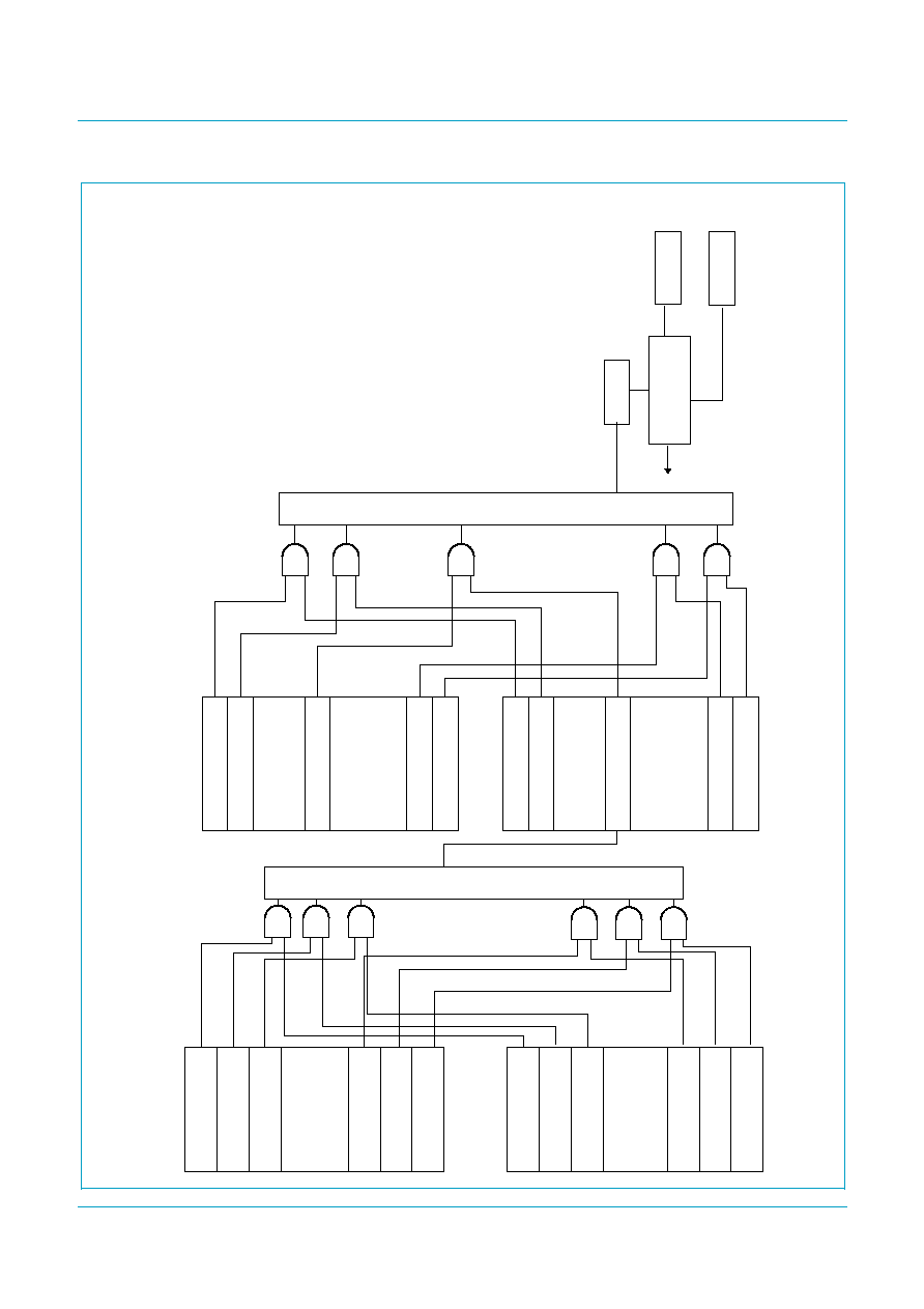
Figure 4
shows the relationship between the interrupt events and pin INT.
Each of the indicated USB and DMA events is logged in a status bit of the Interrupt
register and the DMA Interrupt Reason register, respectively. Corresponding bits in
the Interrupt Enable register and the DMA Interrupt Enable register determine
whether or not an event will generate an interrupt.
Interrupts can be masked globally by means of bit GLINTENA of the Mode register.
Field CDBGMOD[1:0] of the Interrupt Configuration register controls the generation
of the INT signals for the control pipe. Field DDBGMODIN[1:0] of the Interrupt
Configuration register controls the generation of the INT signals for the IN pipe. Field
DDBGMODOUT[1:0] of the Interrupt Configuration register controls the generation of
the INT signals for the OUT pipe; see
Table 26
.
8.12.2
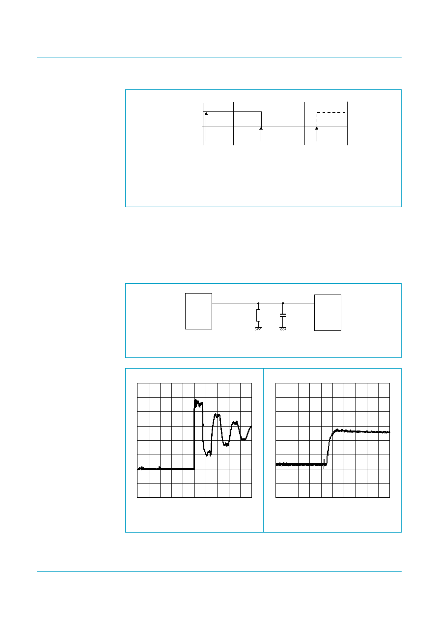
Interrupt control
Bit GLINTENA in the Mode register is a global enable/disable bit. The behavior of this
bit is given in
Figure 5
.
Event A: When an interrupt event occurs (for example, SOF interrupt) with
bit GLINTENA set to logic 0, an interrupt will not be generated at pin INT. It will,
however, be registered in the corresponding Interrupt register bit.
Event B: When bit GLINTENA is set to logic 1, pin INT is asserted because bit SOF in
the Interrupt register is already set.
Event C: If the firmware sets bit GLINTENA to logic 0, pin INT will still be asserted.
The bold dashed line shows the desired behavior of pin INT.
Deassertion of pin INT can be achieved either by clearing all the Interrupt register or
the DMA Interrupt Reason register, depending on the event.
Remark: When clearing an interrupt event, perform write to all the bytes of the
register.
For more information on interrupt control, see
Section 9.2.2
,
Section 9.2.5
and
Section 9.5.1
.
xxxxxxxxxxxxxxxxxxxxx xxxxxxxxxxxxxxxxxxxxxxxxxx xxxxxxx x x x xxxxxxxxxxxxxxxxxxxxxxxxxxxxxx xxxxxxxxxxxxxxxxxxx xx xx
xxxxx xxxxxxxxxxxxxxxxxxxxxxxxxxx xxxxxxxxxxxxxxxxxxx xxxxxx xxxxxxxxxxxxxxxxxxxxxxxxxxxxxxxxxxx xxxxxxxxxxxx x x
xxxxxxxxxxxxxxxxxxxxx xxxxxxxxxxxxxxxxxxxxxxxxxxxxxx xxxxx xxxxxxxxxxxxxxxxxxxxxxxxxxxxxxxxxxxxxxxxxxxxxxxxxx xxxxxxxx
xxxxxxxxxxxxxxxxxxxxxxxxx xxxxxxxxxxxxxxxxxxxx xxx
Philips Semiconductor
s
ISP1583
Hi-Speed USB peripheral contr
oller
9397 750 13461
© K
oninklijk
e Philips Electronics N.V
. 2004. All r
ights reser
v
ed.
Pr
oduct data
Re
v
.
03 -- 12 J
u
l
y
2004
18 of 87
Fig 4.
Interrupt logic.
BSY_DONE
OR
Interrupt register
DMA Interrupt Reason
register
DMA Interrupt Enable
register
Interrupt Enable register
TF_RD_DONE
CMD_INTRQ_OK
GDMA_STOP
EXT_EOT
INT_EOT
IE_BSY_DONE
IE_TF_RD_DONE
IE_CMD_INTRQ_OK
IE_GDMA_STOP
IE_EXT_EOT
IE_INT_EOT
......
......
......
..............
OR
IEBRST
IESOF
IEDMA
IEP7RX
IEP7TX
BRESET
SOF
DMA
EP7RX
EP7TX
......
....
......
....
......
....
004aaa267
LATCH
GLINTENA
INTPOL
LE
Interrupt Configuration
register
Mode register
INT
PULSE OR LEVEL
GENERATOR
Philips Semiconductors
ISP1583
Hi-Speed USB peripheral controller
Product data
Rev. 03 -- 12 July 2004
19 of 87
9397 750 13461
© Koninklijke Philips Electronics N.V. 2004. All rights reserved.
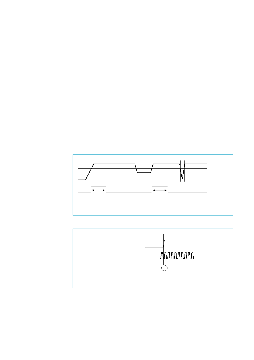
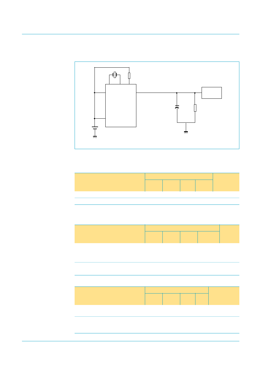
8.13 V
BUS
sensing
The V
BUS
pin is one of the ways to wake up the clock when the ISP1583 is suspended
with bit CLKAON set to logic 0 (clock off option).
To detect whether the host is connected or not, that is V
BUS
sensing, a 1 M
resistor
and a 1
µ
F electrolytic capacitor must be added to damp the overshoot upon plug-in.
Pin INT: HIGH = deassert; LOW = assert (individual interrupts are enabled).
Fig 5.
Behavior of bit GLINTENA.
INT pin
004aaa394
GLINTENA = 0
SOF asserted
GLINTENA = 1
SOF asserted
GLINTENA = 0
(during this time,
an interrupt event
occurs. For example,
SOF asserted.)
A
B
C
Fig 6.
Resistor and electrolytic capacitor needed for V
BUS
sensing.
Fig 7.
Oscilloscope reading: no resistor
and capacitor in the network.
Fig 8.
Oscilloscope reading: with
resistor and capacitor in the
network.
1 M
ISP1583
004aaa449
+
1 µF
55
USB
Connector
004aaa441
004aaa442
Philips Semiconductors
ISP1583
Hi-Speed USB peripheral controller
Product data
Rev. 03 -- 12 July 2004
20 of 87
9397 750 13461
© Koninklijke Philips Electronics N.V. 2004. All rights reserved.
8.14 Power-on reset
The ISP1583 requires a minimum pulse width of 500
µ
s.
The RESET_N pin can be either connected to V
CC(3V3)
(using the internal POR
circuit) or externally controlled (by the microcontroller, ASIC, and so on). When
V
CC(3V3)
is directly connected to the RESET_N pin, the internal pulse width t
PORP
will
be typically 200 ns.
The power-on reset function can be explained by viewing the dips at t2-t3 and t4-t5
on the V
CC(POR)
curve (
Figure 9
).
t0 -- The internal POR starts with a HIGH level.
t1 -- The detector will see the passing of the trip level and a delay element will add
another t
PORP
before it drops to LOW.
t2-t3 -- The internal POR pulse will be generated whenever V
CC(POR)
drops below
V
trip
for more than 11
µ
s.
t4-t5 -- The dip is too short (< 11
µ
s) and the internal POR pulse will not react and
will remain LOW.
Figure 10
shows the availability of the clock with respect to the external POR.
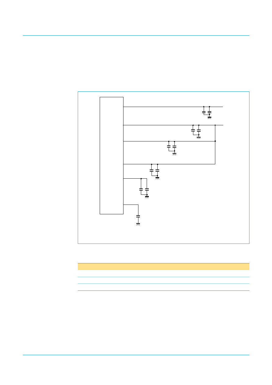
8.15 Power supply
The ISP1583 can be powered by 3.3 V
±
0.3 V, and from 1.65 V to 3.6 V at the
interface. For connection details, see
Figure 11
.
(1) PORP = power-on reset pulse.
Fig 9.
POR timing.
Stable external clock is to be available at A.
Fig 10. Clock with respect to the external POR.
004aaa389
VBAT(POR)
t0
t1
t2
t3
t4
t5
Vtrip
t
PORP
PORP(1)
t
PORP
POR
EXTERNAL CLOCK
A
004aaa365
Philips Semiconductors
ISP1583
Hi-Speed USB peripheral controller
Product data
Rev. 03 -- 12 July 2004
21 of 87
9397 750 13461
© Koninklijke Philips Electronics N.V. 2004. All rights reserved.
If the ISP1583 is powered by V
CC(3V3)
= 3.3 V, an integrated 3.3 V-to-1.8 V voltage
regulator provides a 1.8 V supply voltage for the internal logic.
In sharing mode (that is, when V
CC(3.3)
is not present and V
CC(I/O)
is present), all the
I/O pins are in 3-state, the interrupt pin is connected to ground, and the suspend pin
is connected to V
CC(I/O)
. See
Table 4
.
Table 5
shows power modes in which the ISP1583 can be operated.
[1]
The power supply to the IC (V
CC(3V3)
) is 3.3 V. Therefore, if the application is bus-powered, a 3.3 V
regulator needs to be used.
[2]
V
CC(I/O)
can range from 1.65 V to 3.6 V. If the application is bus-powered, a voltage regulator needs to
be used.
(1) It is mandatory to use a 4.7
µ
F electrolytic capacitor on pin 56.
Fig 11. ISP1583 with 3.3 V supply.
Table 5:
Power modes
V
CC(3V3)
V
CC(I/O)
Power mode
V
BUS
[1]
V
BUS
[2]
bus-powered
Self-powered
self-powered
self-powered
V
BUS
[1]
self-powered
power-sharing (hybrid)
004aaa271
61
VCC(I/O)
ISP1583
3.3 V
± 0.
3 V
VCC(I/O)
VCC(3V3)
26
41
VCC(I/O)
VCC(1V8)
54
56
4.7 µF(1)
0.1 µF
0.01 µF
0.1 µF
0.01 µF
0.1 µF
1.65 V to 3.6 V
0.01 µF
0.1 µF
0.01 µF
0.1 µF
VCC(1V8)
32
0.1 µF
+
Philips Semiconductors
ISP1583
Hi-Speed USB peripheral controller
Product data
Rev. 03 -- 12 July 2004
22 of 87
9397 750 13461
© Koninklijke Philips Electronics N.V. 2004. All rights reserved.
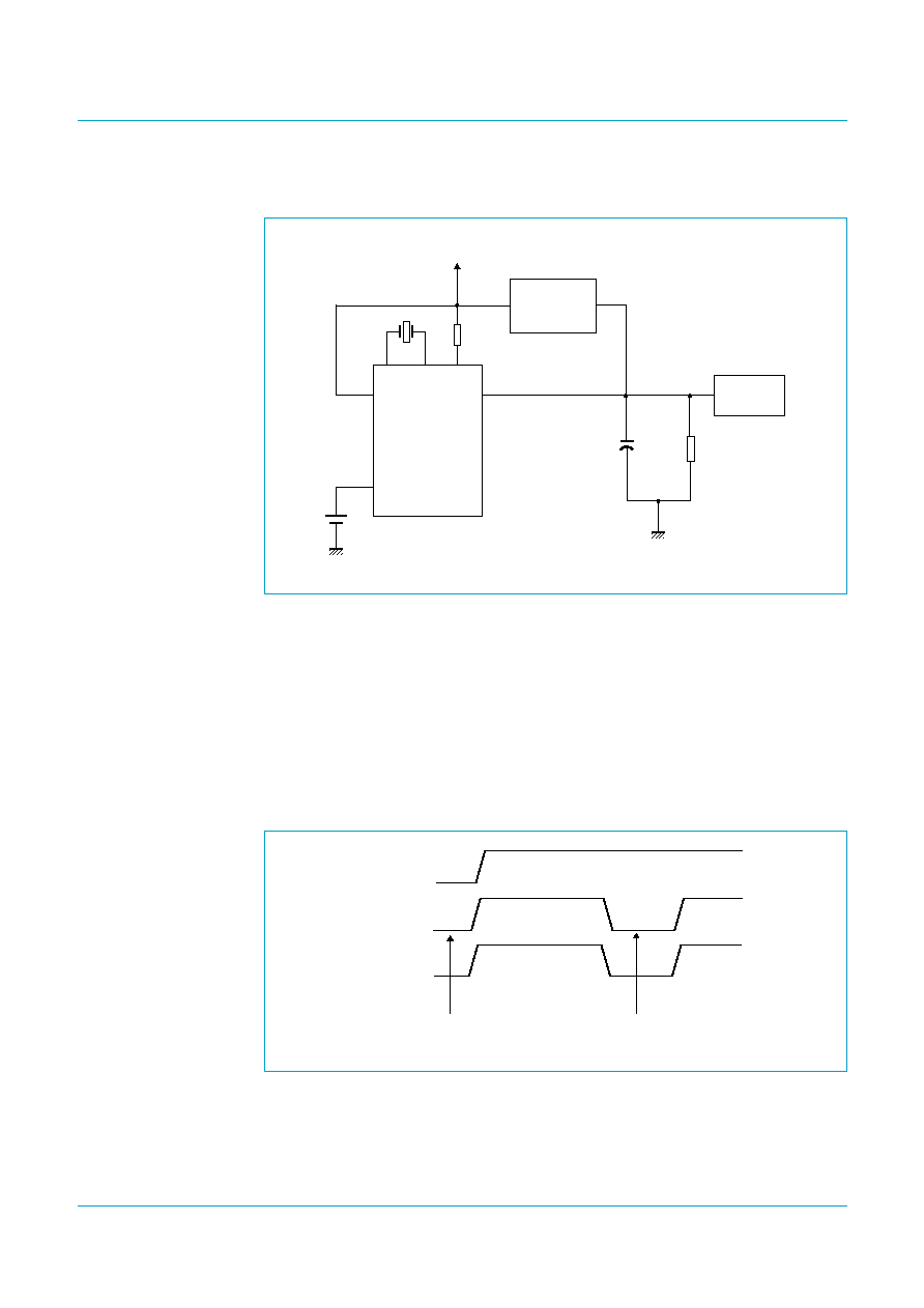
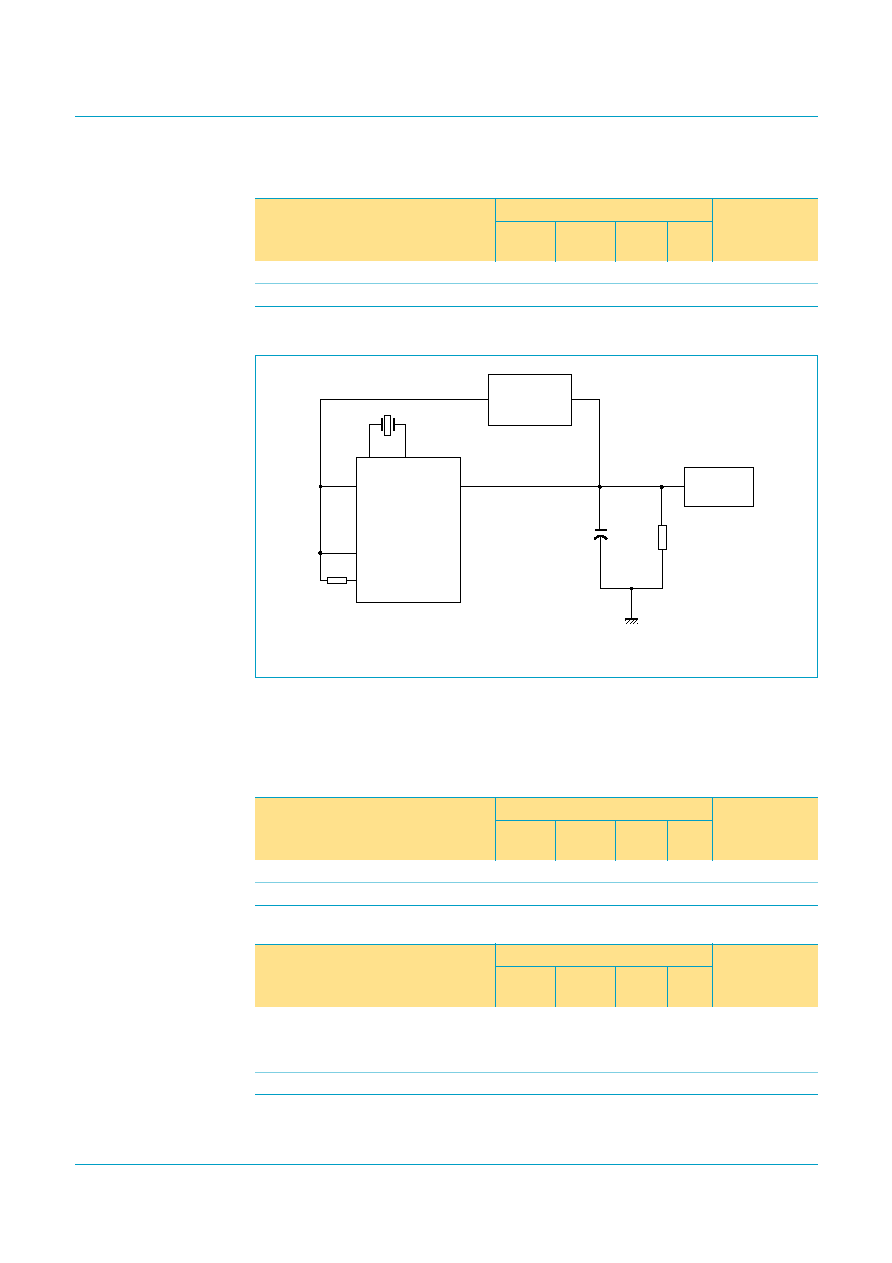
8.15.1
Power-sharing mode
As can be seen in
Figure 12
, in power-sharing mode, V
CC(3V3)
is supplied by the
output of the 5 V-to-3.3 V voltage regulator. The input to the regulator is from V
BUS
.
V
CC(I/O)
is supplied through the power source of the system. When the USB cable is
plugged in, the ISP1583 goes through the power-on reset cycle. In this mode, OTG is
disabled.
The processor will experience continuous interrupt because the default status of the
interrupt pin when operating in sharing mode with the V
BUS
not present is LOW. To
overcome this, implement external V
BUS
sensing circuitry. The output from the voltage
regulator can be connected to pin GPIO of the processor to qualify the interrupt from
the ISP1583.
Fig 12. Power-sharing mode.
Fig 13. Interrupt pin status during power off in power-sharing mode.
004aaa458
ISP1583
+
-
5 V-to-3.3 V
USB
VOLTAGE
REGULATOR
To GPIO of processor
for sensing VBUS
1 M
VCC(3V3)
VCC(I/O)
VBUS
RPU
VBUS
1 µF
1.5 k
+
-
004aaa459
VCC(I/O)
VCC(3V3)
INT
power off
power off

Philips Semiconductors
ISP1583
Hi-Speed USB peripheral controller
Product data
Rev. 03 -- 12 July 2004
23 of 87
9397 750 13461
© Koninklijke Philips Electronics N.V. 2004. All rights reserved.
Table 6:
Operation truth table for SoftConnect
ISP1583 operation
Power supply
Bit SOFTCT in
Mode register
V
CC(3V3)
V
CC(I/O)
RPU
(3.3 V)
V
BUS
Normal bus operation
3.3 V
3.3 V
3.3 V
5 V
enabled
Core power is lost
0 V
3.3 V
0 V
0 V
not applicable
Table 7:
Operation truth table for clock off during suspend
ISP1583 operation
Power supply
Clock off
during
suspend
V
CC(3V3)
V
CC(I/O)
RPU
(3.3 V)
V
BUS
Clock will wake up:
After a resume and
After a bus reset
3.3 V
3.3 V
3.3 V
5 V
enabled
Core power is lost
0 V
3.3 V
0 V
0 V
not applicable
Table 8:
Operation truth table for back voltage compliance
ISP1583 operation
Power supply
Bit SOFTCT
in Mode
register
V
CC(3V3)
V
CC(I/O)
RPU
(3.3 V)
V
BUS
Back voltage is not measured in this
mode
3.3 V
3.3 V
3.3 V
5 V
enabled
Back voltage is not an issue because
core power is lost
0 V
3.3 V
0 V
0 V
not
applicable
Table 9:
Operation truth table for OTG
ISP1583 operation
Power supply
OTG
register
V
CC(3V3)
V
CC(I/O)
RPU
(3.3 V)
V
BUS
SRP is not applicable
3.3 V
3.3 V
3.3 V
5 V
not
applicable
OTG is not possible because V
BUS
is
not present and so core power is lost
0 V
3.3 V
0 V
0 V
not
applicable
Philips Semiconductors
ISP1583
Hi-Speed USB peripheral controller
Product data
Rev. 03 -- 12 July 2004
24 of 87
9397 750 13461
© Koninklijke Philips Electronics N.V. 2004. All rights reserved.
8.15.2
Self-powered mode
In self-powered mode, V
CC(3V3)
and V
CC(I/O)
are supplied by the system. Bit SOFTCT
in the Mode register must be always logic 1. See
Figure 14
.
[1]
When the USB cable is removed, SoftConnect is disabled.
Fig 14. Self-powered mode.
Table 10:
Operation truth table for SoftConnect
ISP1583 operation
Power supply
Bit SOFTCT
in Mode
register
V
CC(3V3)
V
CC(I/O)
RPU
(3.3 V)
V
BUS
Normal bus operation
3.3 V
3.3 V
3.3 V
5 V
enabled
No pull-up on DP
3.3 V
3.3 V
3.3 V
0 V
[1]
disabled
Table 11:
Operation truth table for clock off during suspend
ISP1583 operation
Power supply
Clock off
during
suspend
V
CC(3V3)
V
CC(I/O)
RPU
(3.3 V)
V
BUS
Clock will wake up:
After a resume and
After a bus reset
3.3 V
3.3 V
3.3 V
5 V
enabled
Clock will wake up:
After detecting the presence of V
BUS
3.3 V
3.3 V
3.3 V
0 V => 5 V enabled
Table 12:
Operation truth table for back voltage compliance
ISP1583 operation
Power supply
Bit SOFTCT in
Mode register
V
CC(3V3)
V
CC(I/O)
RPU
(3.3 V)
V
BUS
Back voltage is not measured in this
mode
3.3 V
3.3 V
3.3 V
5 V
enabled
Back voltage is not an issue because
pull-up on DP will not be present when
V
BUS
is not present
3.3 V
3.3 V
3.3 V
0 V
disabled
004aaa461
ISP1583
+
-
USB
1 M
VCC(3V3)
VCC(I/O)
VBUS
RPU
VBUS
1 µF
1.5 k
+
-
Philips Semiconductors
ISP1583
Hi-Speed USB peripheral controller
Product data
Rev. 03 -- 12 July 2004
25 of 87
9397 750 13461
© Koninklijke Philips Electronics N.V. 2004. All rights reserved.
8.15.3
Bus-powered mode
In bus-powered mode (see
Figure 15
), V
CC(3V3)
and V
CC(I/O)
are supplied by the
output of the 5 V-to-3.3 V voltage regulator. The input to the regulator is from V
BUS
.
On plugging in of the USB cable, the ISP1583 goes through the power-on reset cycle.
In this mode, OTG is disabled.
Table 13:
Operation truth table for OTG
ISP1583 operation
Power supply
OTG register
V
CC(3V3)
V
CC(I/O)
RPU
(3.3 V)
V
BUS
SRP is not applicable
3.3 V
3.3 V
3.3 V
5 V
not applicable
SRP is possible
3.3 V
3.3 V
3.3 V
0 V
operational
Fig 15. Bus-powered mode.
Table 14:
Operation truth table for SoftConnect
ISP1583 operation
Power supply
Bit SOFTCT in
Mode register
V
CC(3V3)
V
CC(I/O)
RPU
(3.3 V)
V
BUS
Normal bus operation
3.3 V
3.3 V
3.3 V
5 V
enabled
Power is lost
0 V
0 V
0 V
0 V
not applicable
Table 15:
Operation truth table for clock off during suspend
ISP1583 operation
Power supply
Clock off
during
suspend
V
CC(3V3)
V
CC(I/O)
RPU
(3.3 V)
V
BUS
Clock will wake up:
After a resume and
After a bus reset
3.3 V
3.3 V
3.3 V
5 V
enabled
Power is lost
0 V
0 V
0 V
0 V
not applicable
004aaa463
ISP1583
5 V-to-3.3 V
USB
VOLTAGE
REGULATOR
1 M
VCC(3V3)
VCC(I/O)
VBUS
VBUS
1 µF
RPU
+
-
1.5 k

Philips Semiconductors
ISP1583
Hi-Speed USB peripheral controller
Product data
Rev. 03 -- 12 July 2004
26 of 87
9397 750 13461
© Koninklijke Philips Electronics N.V. 2004. All rights reserved.
Table 16:
Operation truth table for back voltage compliance
ISP1583 operation
Power supply
Bit SOFTCT in
Mode register
V
CC(3V3)
V
CC(I/O)
RPU
(3.3 V)
V
BUS
Back voltage is not measured in this
mode
3.3 V
3.3 V
3.3 V
5 V
enabled
Power is lost
0 V
0 V
0 V
0 V
not applicable
Table 17:
Operation truth table for OTG
ISP1583 operation
Power supply
OTG register
V
CC(3V3)
V
CC(I/O)
RPU
(3.3 V)
V
BUS
SRP is not applicable
3.3 V
3.3 V
3.3 V
5 V
not applicable
Power is lost
0 V
0 V
0 V
0 V
not applicable

Philips Semiconductors
ISP1583
Hi-Speed USB peripheral controller
Product data
Rev. 03 -- 12 July 2004
27 of 87
9397 750 13461
© Koninklijke Philips Electronics N.V. 2004. All rights reserved.
9.
Register description
Table 18:
Register overview
Name
Destination
Address
Description
Size
(bytes)
Reference
Initialization registers
Address
device
00h
USB device address and enable
1
Section 9.2.1
on page 29
Mode
device
0Ch
power-down options, global interrupt
enable, SoftConnect
1
Section 9.2.2
on page 29
Interrupt Configuration
device
10h
interrupt sources, trigger mode,
output polarity
1
Section 9.2.3
on page 32
OTG
device
12h
OTG implementation
1
Section 9.2.4
on page 32
Interrupt Enable
device
14h
interrupt source enabling
4
Section 9.2.5
on page 34
Data flow registers
Endpoint Index
endpoints
2Ch
endpoint selection, data flow direction 1
Section 9.3.1
on page 36
Control Function
endpoint
28h
endpoint buffer management
1
Section 9.3.2
on page 37
Data Port
endpoint
20h
data access to endpoint FIFO
2
Section 9.3.3
on page 38
Buffer Length
endpoint
1Ch
packet size counter
2
Section 9.3.4
on page 39
Buffer Status
endpoint
1Eh
buffer status for each endpoint
1
Section 9.3.5
on page 40
Endpoint MaxPacketSize
endpoint
04h
maximum packet size
2
Section 9.3.6
on page 41
Endpoint Type
endpoint
08h
selects endpoint type: control,
isochronous, bulk or interrupt
2
Section 9.3.7
on page 42
DMA registers
DMA Command
DMA controller
30h
controls all DMA transfers
1
Section 9.4.1
on page 44
DMA Transfer Counter
DMA controller
34h
sets byte count for DMA transfer
4
Section 9.4.2
on page 46
DMA Configuration
DMA controller
38h
byte 0: sets GDMA configuration
(counter enable, burst length, data
strobing, bus width)
1
Section 9.4.3
on page 47
39h
byte 1: sets ATA configuration
(IORDY enable, mode selection:
ATA/MDMA/PIO)
1
DMA Hardware
DMA controller
3Ch
endian type, master or slave
selection, signal polarity for DACK,
DREQ, DIOW, DIOR
1
Section 9.4.4
on page 49

Philips Semiconductors
ISP1583
Hi-Speed USB peripheral controller
Product data
Rev. 03 -- 12 July 2004
28 of 87
9397 750 13461
© Koninklijke Philips Electronics N.V. 2004. All rights reserved.
9.1 Register access
Register access depends on the bus width used:
·
8-bit bus: multi-byte registers are accessed lower byte (LSByte) first
·
16-bit bus: for single-byte registers, the upper byte (MSByte) must be ignored.
Endpoint specific registers are indexed via the Endpoint Index register. The target
endpoint must be selected before accessing the following registers:
Task File 1F0
ATAPI peripheral
40h
single address word register: byte 0
(lower byte) is accessed first
2
Section 9.4.5
on page 50
Task File 1F1
ATAPI peripheral
48h
IDE device access
1
Task File 1F2
ATAPI peripheral
49h
IDE device access
1
Task File 1F3
ATAPI peripheral
4Ah
IDE device access
1
Task File 1F4
ATAPI peripheral
4Bh
IDE device access
1
Task File 1F5
ATAPI peripheral
4Ch
IDE device access
1
Task File 1F6
ATAPI peripheral
4Dh
IDE device access
1
Task File 1F7
ATAPI peripheral
44h
IDE device access (write only;
reading returns FFh)
1
Task File 3F6
ATAPI peripheral
4Eh
IDE device access
1
Task File 3F7
ATAPI peripheral
4Fh
IDE device access
1
DMA Interrupt Reason
DMA controller
50h
shows reason (source) for DMA
interrupt
2
Section 9.4.6
on page 53
DMA Interrupt Enable
DMA controller
54h
enables DMA interrupt sources
2
Section 9.4.7
on page 55
DMA Endpoint
DMA controller
58h
selects endpoint FIFO, data flow
direction
1
Section 9.4.8
on page 56
DMA Strobe Timing
DMA controller
60h
strobe duration in MDMA mode
1
Section 9.4.9
on page 56
DMA Burst Counter
DMA controller
64h
DMA burst length
2
Section 9.4.10
on page 57
General registers
Interrupt
device
18h
shows interrupt sources
4
Section 9.5.1
on page 57
Chip ID
device
70h
product ID code and hardware
version
3
Section 9.5.2
on page 59
Frame Number
device
74h
last successfully received Start Of
Frame: lower byte (byte 0) is
accessed first
2
Section 9.5.3
on page 60
Scratch
device
78h
allows save or restore of firmware
status during suspend
2
Section 9.5.4
on page 60
Unlock Device
device
7Ch
re-enables register access after
`suspend'
2
Section 9.5.5
on page 61
Test Mode
PHY
84h
direct setting of the DP and DM
states, internal transceiver test (PHY)
1
Section 9.5.6
on page 62
Table 18:
Register overview
...continued
Name
Destination
Address
Description
Size
(bytes)
Reference

Philips Semiconductors
ISP1583
Hi-Speed USB peripheral controller
Product data
Rev. 03 -- 12 July 2004
29 of 87
9397 750 13461
© Koninklijke Philips Electronics N.V. 2004. All rights reserved.
·
Buffer Length
·
Buffer Status
·
Control Function
·
Data Port
·
Endpoint MaxPacketSize
·
Endpoint Type.
Remark: All reserved bits are not implemented. The bus and bus reset values are not
defined. Therefore, writing to these reserved bits will have no effect.
9.2 Initialization registers
9.2.1
Address register (address: 00h)
This register sets the USB assigned address and enables the USB device.
Table 19
shows the Address register bit allocation.
Bits DEVADDR will be cleared whenever a bus reset, a power-on reset or a soft reset
occurs. Bit DEVEN will be cleared whenever a power-on reset or a soft reset occurs,
and will be set after a bus reset.
In response to the standard USB request SET_ADDRESS, the firmware must write
the (enabled) device address to the Address register, followed by sending an empty
packet to the host. The new device address is activated when the device receives
acknowledgment from the host.
9.2.2
Mode register (address: 0Ch)
This register consists of 2 bytes (bit allocation: see
Table 21
).
The Mode register controls resume, suspend and wake-up behavior, interrupt activity,
soft reset, clock signals and SoftConnect operation.
Table 19:
Address register: bit allocation
Bit
7
6
5
4
3
2
1
0
Symbol
DEVEN
DEVADDR[6:0]
Reset
0
0
0
0
0
0
0
0
Bus reset
1
0
0
0
0
0
0
0
Access
R/W
R/W
R/W
R/W
R/W
R/W
R/W
R/W
Table 20:
Address register: bit description
Bit
Symbol
Description
7
DEVEN
Logic 1 enables the device.
6 to 0
DEVADDR[6:0]
This field specifies the USB device address.

Philips Semiconductors
ISP1583
Hi-Speed USB peripheral controller
Product data
Rev. 03 -- 12 July 2004
30 of 87
9397 750 13461
© Koninklijke Philips Electronics N.V. 2004. All rights reserved.
Table 21:
Mode register: bit allocation
Bit
15
14
13
12
11
10
9
8
Symbol
TEST2
TEST1
TEST0
reserved
DMA
CLKON
VBUSSTAT
Reset
-
-
-
-
-
-
0
-
Bus reset
-
-
-
-
-
-
0
-
Access
R
R
R
R
R
R
R/W
R
Bit
7
6
5
4
3
2
1
0
Symbol
CLKAON
SNDRSU
GOSUSP
SFRESET
GLINTENA
WKUPCS
PWRON
SOFTCT
Reset
0
0
0
0
0
0
0
0
Bus reset
0
0
0
0
unchanged
0
0
unchanged
Access
R/W
R/W
R/W
R/W
R/W
R/W
R/W
R/W
Table 22:
Mode register: bit description
Bit
Symbol
Description
15
TEST2
This bit reflects the MODE1 pin setting. Only for test purposes.
14
TEST1
This bit reflects the MODE0 pin setting. Only for test purposes.
13
TEST0
This bit reflects the BUS_CONF pin setting. Only for test
purposes.
12 to 10
-
reserved
9
DMACLKON
0 -- Power save mode; the DMA circuit will stop completely to
save power.
1 -- Supply clock to the DMA circuit.
8
VBUSSTAT
This bit reflects the V
BUS
pin status.
7
CLKAON
Clock Always On: Logic 1 indicates that the internal clocks are
always running when in the suspend state. Logic 0 switches off
the internal oscillator and PLL when the device goes into suspend
mode. The device will consume less power if this bit is set to
logic 0. The clock is stopped after a delay of approximately 2 ms,
following which bit GOSUSP is set.
6
SNDRSU
Send Resume: Writing logic 1, followed by logic 0 will generate
an upstream resume signal of 10 ms duration, after a 5 ms delay.
5
GOSUSP
Go Suspend: Writing logic 1, followed by logic 0 will activate
suspend mode.
4
SFRESET
Soft Reset: Writing logic 1, followed by logic 0 will enable a
software-initiated reset to the ISP1583. A soft reset is similar to a
hardware-initiated reset (via the RESET_N pin).

Philips Semiconductors
ISP1583
Hi-Speed USB peripheral controller
Product data
Rev. 03 -- 12 July 2004
31 of 87
9397 750 13461
© Koninklijke Philips Electronics N.V. 2004. All rights reserved.
When SoftConnect and V
BUS
are not present (except in OTG), the USB bus activities
are not qualified. Therefore, the chip will follow the suspend command to enter
suspend mode (the clock is controlled by bit CLKAON).
When V
BUS
is off, the 1.5 k
pull-up resister is disconnected from pin DP in
approximately 4 ns via bit SOFTCT in the Mode register and a suspend interrupt is
set with some latency (debounce and disqualify USB traffic).
When bit SOFTCT is set to logic 0, no interrupt is generated. The firmware can issue
a suspend command, followed by the resetting of bit SOFTCT to suspend the chip.
If OTG is logic 1, the pull-up resistor on pin DP depends on D+ line (V
BUS
sensing
status). Bit DP operates as normal, so the firmware must mask suspend and wake-up
interrupt events. When SRP is completed, the device should clear OTG.
If OTG is logic 0, the status of the pull-up resistor on DP is referred to in
Table 23
.
3
GLINTENA
Global Interrupt Enable: Logic 1 enables all interrupts. Individual
interrupts can be masked by clearing the corresponding bits in the
Interrupt Enable register.
When this bit is not set, an unmasked interrupt will not generate
an interrupt trigger on the interrupt pin. If global interrupt, however,
is enabled while there is any pending unmasked interrupt, an
interrupt signal will be immediately generated on the interrupt pin.
(If the interrupt is set to pulse mode, the interrupt events that were
generated before the global interrupt is enabled may be dropped.)
2
WKUPCS
Wake-up on Chip selection: Logic 1 enables wake-up from
suspend mode through a valid register read on the ISP1583. (A
read will invoke the chip clock to restart. If you write to the register
before the clock gets stable, it may cause malfunctioning.)
1
PWRON
The SUSPEND pin output control.
0 -- The SUSPEND pin is HIGH when the ISP1583 is in the
suspend state. Otherwise, the SUSPEND pin is LOW.
1 -- When the device is woken up from the suspend state, there
will be a 1 ms active HIGH pulse on the SUSPEND pin. The
SUSPEND pin will remain LOW in all other states.
0
SOFTCT
SoftConnect: Logic 1 enables the connection of the 1.5 k
pull-up resistor on pin RPU to the DP line. Bus reset
value: unchanged.
Table 23:
Status of the chip
V
BUS
SoftConnect = on
SoftConnect = off
On
pull-up resistor on DP
pull-up resistor on DP is removed;
suspend interrupt is immediately set,
regardless of the D+ and D
-
signals
Off
pull-up resistor on DP is removed;
suspend interrupt is immediately set,
regardless of the D+ and D
-
signals
pull-up resistor on DP is removed;
suspend interrupt is immediately set,
regardless of the D+ and D
-
signals
Table 22:
Mode register: bit description
...continued
Bit
Symbol
Description

Philips Semiconductors
ISP1583
Hi-Speed USB peripheral controller
Product data
Rev. 03 -- 12 July 2004
32 of 87
9397 750 13461
© Koninklijke Philips Electronics N.V. 2004. All rights reserved.
9.2.3
Interrupt Configuration register (address: 10h)
This 1-byte register determines the behavior and polarity of the INT output. The bit
allocation is shown in
Table 24
. When the USB SIE receives or generates an ACK,
NAK or STALL, it will generate interrupts depending on three Debug mode fields.
CDBGMOD[1:0] -- interrupts for the control endpoint 0
DDBGMODIN[1:0] -- interrupts for the DATA IN endpoints 1 to 7
DDBGMODOUT[1:0] -- interrupts for the DATA OUT endpoints 1 to 7.
The Debug mode settings for CDBGMOD, DDBGMODIN and DDBGMODOUT allow
you to individually configure when the ISP1583 sends an interrupt to the external
microprocessor.
Table 26
lists the available combinations.
Bit INTPOL controls the signal polarity of the INT output: active HIGH or LOW, rising
or falling edge. For level-triggering, bit INTLVL must be made logic 0. By setting
INTLVL to logic 1, an interrupt will generate a pulse of 60 ns (edge-triggering).
[1]
First NAK: the first NAK on an IN or OUT token after a previous ACK response.
9.2.4
OTG register (address: 12h)
The bit allocation of the OTG register is given in
Table 27
.
Table 24:
Interrupt Configuration register: bit allocation
Bit
7
6
5
4
3
2
1
0
Symbol
CDBGMOD[1:0]
DDBGMODIN[1:0]
DDBGMODOUT[1:0]
INTLVL
INTPOL
Reset
1
1
1
1
1
1
0
0
Bus reset
1
1
1
1
1
1
unchanged
unchanged
Access
R/W
R/W
R/W
R/W
R/W
R/W
R/W
R/W
Table 25:
Interrupt Configuration register: bit description
Bit
Symbol
Description
7 to 6
CDBGMOD[1:0]
Control 0 Debug Mode: For values, see
Table 26
5 to 4
DDBGMODIN[1:0]
Data Debug Mode IN: For values, see
Table 26
3 to 2
DDBGMODOUT[1:0]
Data Debug Mode OUT: For values, see
Table 26
1
INTLVL
Interrupt Level: Selects signaling mode on output INT
(0 = level; 1 = pulsed). In pulsed mode, an interrupt
produces a 60 ns pulse. Bus reset value: unchanged.
0
INTPOL
Interrupt Polarity: Selects signal polarity on output INT
(0 = active LOW, 1 = active HIGH). Bus reset
value: unchanged.
Table 26:
Debug mode settings
Value
CDBGMOD
DDBGMODIN
DDBGMODOUT
00h
interrupt on all ACK and
NAK
interrupt on all ACK and
NAK
interrupt on all ACK, NYET
and NAK
01h
interrupt on all ACK.
interrupt on ACK
interrupt on ACK and NYET
1Xh
interrupt on all ACK and
first NAK
[1]
interrupt on all ACK and
first NAK
[1]
interrupt on all ACK, NYET
and first NAK
[1]

Philips Semiconductors
ISP1583
Hi-Speed USB peripheral controller
Product data
Rev. 03 -- 12 July 2004
33 of 87
9397 750 13461
© Koninklijke Philips Electronics N.V. 2004. All rights reserved.
Table 27:
OTG register: bit allocation
Bit
7
6
5
4
3
2
1
0
Symbol
reserved
DP
BSESSVALID
INITCOND
DISCV
VP
OTG
Reset
-
-
0
-
-
0
0
0
Bus reset
-
-
0
-
-
0
0
0
Access
-
-
R/W
R/W
R/W
R/W
R/W
R/W
Table 28:
OTG register: bit description
[1]
Bit
Symbol
Description
7 to 6
-
reserved
5
DP
When set, data-line pulsing is started. The default value of this bit is
logic 0. This bit must be cleared when data-line pulsing is completed.
4
BSESSVALID
The device can initiate another V
BUS
discharge sequence after
data-line pulsing and V
BUS
pulsing, and before it clears this bit and
detects a session valid.
This bit is latched to logic 1 once V
BUS
exceeds the B-device session
valid threshold. Once set, it remains at logic 1. To clear this bit, write
logic 1. (The ISP1583 continuously updates this bit to logic 1 when
the B-session is valid. If the B-session is valid after it is cleared, it is
set back to logic 1 by the ISP1583).
0 -- It implies that SRP has failed. To proceed to a normal operation,
the device can restart SRP, clear bit OTG or proceed to an error
handling process.
1 -- It implies that the B-session is valid. The device clears bit OTG,
goes into normal operation mode, and sets bit SOFTCT (DP pull-up)
in the Mode register. The OTG host has a maximum of 5 s before it
responds to a session request. During this period, the ISP1583 may
request to suspend. Therefore, the device firmware must wait for
sometime if it wishes to know the SRP result (success--if there is
minimum response from the host within 5 s; failure--if there is no
response from the host within 5 s).
3
INITCOND
Write logic 1 to clear this bit. The device clears this bit, and waits for
more than 2 ms to check the bit status. If it reads logic 0, it means
that V
BUS
remains lower than 0.8 V, and DP or DM at SE0 during the
elapsed time is cleared. The device can then start a B-device SRP. If
it reads logic 1, it means that the initial condition of an SRP is
violated. So, the device should abort SRP.
The bit is set to logic 1 by the ISP1583 when initial conditions are not
met, and only writing logic 1 clears the bit. (If initial conditions are not
met after this bit has been cleared, it will be set again).
Remark: This implementation does not cover the case if an initial
SRP condition is violated when this bit is read and data-line pulsing
is started.

Philips Semiconductors
ISP1583
Hi-Speed USB peripheral controller
Product data
Rev. 03 -- 12 July 2004
34 of 87
9397 750 13461
© Koninklijke Philips Electronics N.V. 2004. All rights reserved.
[1]
No interrupt is designed for OTG. The V
BUS
interrupt, however, may assert as a side effect during the
V
BUS
pulsing (see note 2).
When OTG is in progress, the V
BUS
interrupt may be set because V
BUS
is charged over V
BUS
sensing
threshold or the OTG host has turned on the V
BUS
supply to the device. Even if the V
BUS
interrupt is
found during SRP, the device should complete data-line pulsing and V
BUS
pulsing before starting the
B_session_valid detection.
OTG implementation applies to the device with self-power capability. If the device works in sharing
mode, it should provide a switch circuit to supply power to the ISP1583 core during SRP.
Session Request Protocol (SRP):
The ISP1583 can initiate an SRP. The B-device initiates SRP by data-line pulsing
followed by V
BUS
pulsing. The A-device can detect either data-line pulsing or V
BUS
pulsing.
The ISP1583 can initiate the B-device SRP by performing the following steps:
1. Detect initial conditions: read bit INITCOND of the OTG register.
2. Start data-line pulsing: set bit DP of the OTG register to logic 1.
3. Wait for 5 ms to 10 ms.
4. Stop data-line pulsing: set bit DP of the OTG register to logic 0.
5. Start V
BUS
pulsing: set bit VP of the OTG register to logic 1.
6. Wait for 10 ms to 20 ms.
7. Stop V
BUS
pulsing: set bit VP of the OTG register to logic 0.
8. Discharge V
BUS
for about 30 ms: optional by using bit DISCV of the OTG register.
9. Detect bit BSESSVALID of the OTG register for a successful SRP with bit OTG
disabled.
The B-device must complete both data-line pulsing and V
BUS
pulsing within 100 ms.
Remark: When disabling, OTG data-line pulsing bit DP and V
BUS
pulsing bit VP must
be cleared by writing logic 1.
9.2.5
Interrupt Enable register (address: 14h)
This register enables or disables individual interrupt sources. The interrupt for each
endpoint can be individually controlled via the associated bits IEPnRX or IEPnTX,
here n represents the endpoint number. All interrupts can be globally disabled
through bit GLINTENA in the Mode register (see
Table 21
).
2
DISCV
Set to logic 1 to discharge V
BUS
. The device discharges V
BUS
before
starting a new SRP. The discharge can take as long as 30 ms for
V
BUS
to be charged less than 0.8 V. This bit must be cleared (write
logic 0) before starting a session end detection.
1
VP
Set to logic 1 to start V
BUS
pulsing. This bit must be set for more than
16 ms and must be cleared before 26 ms.
0
OTG
1 -- Enables the OTG function. The V
BUS
sensing functionality will
be bypassed.
0 -- Normal operation. All OTG control bits will be masked. Status
bits are undefined.
Table 28:
OTG register: bit description
[1]
...continued
Bit
Symbol
Description

Philips Semiconductors
ISP1583
Hi-Speed USB peripheral controller
Product data
Rev. 03 -- 12 July 2004
35 of 87
9397 750 13461
© Koninklijke Philips Electronics N.V. 2004. All rights reserved.
An interrupt is generated when the USB SIE receives or generates an ACK or NAK
on the USB bus. The interrupt generation depends on Debug mode settings of bit
fields CDBGMOD[1:0], DDBGMODIN[1:0] and DDBGMODOUT[1:0].
All data IN transactions use the Transmit buffers (TX), which are handled by bits
DDBGMODIN. All data OUT transactions go via the Receive buffers (RX), which are
handled by bits DDBGMODOUT. Transactions on control endpoint 0 (IN, OUT and
SETUP) are handled by bits CDBGMOD.
Interrupts caused by events on the USB bus (SOF, Pseudo SOF, suspend, resume,
bus reset, setup and high-speed status) can also be individually controlled. A bus
reset disables all enabled interrupts except bit IEBRST (bus reset), which remains
unchanged.
The Interrupt Enable register consists of 4 bytes. The bit allocation is given in
Table 29
.
Table 29:
Interrupt Enable register: bit allocation
Bit
31
30
29
28
27
26
25
24
Symbol
reserved
IEP7TX
IEP7RX
Reset
-
-
-
-
-
-
0
0
Bus Reset
-
-
-
-
-
-
0
0
Access
-
-
-
-
-
-
R/W
R/W
Bit
23
22
21
20
19
18
17
16
Symbol
IEP6TX
IEP6RX
IEP5TX
IEP5RX
IEP4TX
IEP4RX
IEP3TX
IEP3RX
Reset
0
0
0
0
0
0
0
0
Bus Reset
0
0
0
0
0
0
0
0
Access
R/W
R/W
R/W
R/W
R/W
R/W
R/W
R/W
Bit
15
14
13
12
11
10
9
8
Symbol
IEP2TX
IEP2RX
IEP1TX
IEP1RX
IEP0TX
IEP0RX
reserved
IEP0SETUP
Reset
0
0
0
0
0
0
-
0
Bus Reset
0
0
0
0
0
0
-
0
Access
R/W
R/W
R/W
R/W
R/W
R/W
R/W
R/W
Bit
7
6
5
4
3
2
1
0
Symbol
IEVBUS
IEDMA
IEHS_STA
IERESM
IESUSP
IEPSOF
IESOF
IEBRST
Reset
0
0
0
0
0
0
0
0
Bus Reset
0
0
0
0
0
0
0
unchanged
Access
R/W
R/W
R/W
R/W
R/W
R/W
R/W
R/W
Table 30:
Interrupt Enable register: bit description
Bit
Symbol
Description
31 to 26
-
reserved
25
IEP7TX
Logic 1 enables interrupt from the indicated endpoint.
24
IEP7RX
Logic 1 enables interrupt from the indicated endpoint.
23
IEP6TX
Logic 1 enables interrupt from the indicated endpoint.
22
IEP6RX
Logic 1 enables interrupt from the indicated endpoint.
21
IEP5TX
Logic 1 enables interrupt from the indicated endpoint.

Philips Semiconductors
ISP1583
Hi-Speed USB peripheral controller
Product data
Rev. 03 -- 12 July 2004
36 of 87
9397 750 13461
© Koninklijke Philips Electronics N.V. 2004. All rights reserved.
9.3 Data flow registers
9.3.1
Endpoint Index register (address: 2Ch)
The Endpoint Index register selects a target endpoint for register access by the
microcontroller. The register consists of 1 byte, and the bit allocation is shown in
Table 31
.
The following registers are indexed:
·
Buffer Length
·
Buffer Status
·
Control Function
·
Data Port
·
Endpoint MaxPacketSize
·
Endpoint Type.
For example, to access the OUT data buffer of endpoint 1 using the Data Port
register, the Endpoint Index register has to be written first with 02h.
Remark: The Endpoint Index register and the DMA Endpoint Index register must not
point to the same endpoint.
20
IEP5RX
Logic 1 enables interrupt from the indicated endpoint.
19
IEP4TX
Logic 1 enables interrupt from the indicated endpoint.
18
IEP4RX
Logic 1 enables interrupt from the indicated endpoint.
17
IEP3TX
Logic 1 enables interrupt from the indicated endpoint.
16
IEP3RX
Logic 1 enables interrupt from the indicated endpoint.
15
IEP2TX
Logic 1 enables interrupt from the indicated endpoint.
14
IEP2RX
Logic 1 enables interrupt from the indicated endpoint.
13
IEP1TX
Logic 1 enables interrupt from the indicated endpoint.
12
IEP1RX
Logic 1 enables interrupt from the indicated endpoint.
11
IEP0TX
Logic 1 enables interrupt from the control IN endpoint 0.
10
IEP0RX
Logic 1 enables interrupt from the control OUT endpoint 0.
9
-
reserved
8
IEP0SETUP Logic 1 enables interrupt for the setup data received on endpoint 0.
7
IEVBUS
Logic 1 enables interrupt for V
BUS
sensing.
6
IEDMA
Logic 1 enables interrupt on DMA status change detection.
5
IEHS_STA
Logic 1 enables interrupt on detection of a high-speed status
change.
4
IERESM
Logic 1 enables interrupt on detection of a resume state.
3
IESUSP
Logic 1 enables interrupt on detection of a suspend state.
2
IEPSOF
Logic 1 enables interrupt on detection of a Pseudo SOF.
1
IESOF
Logic 1 enables interrupt on detection of an SOF.
0
IEBRST
Logic 1 enables interrupt on detection of a bus reset.
Table 30:
Interrupt Enable register: bit description
...continued
Bit
Symbol
Description

Philips Semiconductors
ISP1583
Hi-Speed USB peripheral controller
Product data
Rev. 03 -- 12 July 2004
37 of 87
9397 750 13461
© Koninklijke Philips Electronics N.V. 2004. All rights reserved.
9.3.2
Control Function register (address: 28h)
The Control Function register performs the buffer management on endpoints. It
consists of 1 byte, and the bit configuration is given in
Table 34
. The register bits can
stall, clear or validate any enabled data endpoint. Before accessing this register, the
Endpoint Index register must be written first to specify the target endpoint.
Table 31:
Endpoint Index register: bit allocation
Bit
7
6
5
4
3
2
1
0
Symbol
reserved
EP0SETUP
ENDPIDX[3:0]
DIR
Reset
-
-
0
0
0
0
0
0
Bus reset
-
-
0
0
0
0
0
0
Access
R/W
R/W
R/W
R/W
R/W
R/W
R/W
R/W
Table 32:
Endpoint Index register: bit description
Bit
Symbol
Description
7 to 6
-
reserved
5
EP0SETUP
Selects the SETUP buffer for endpoint 0.
0 -- EP0 data buffer
1 -- SETUP buffer.
Must be logic 0 for access to other endpoints than endpoint 0.
4 to 1
ENDPIDX[3:0] Endpoint Index: Selects the target endpoint for register access
of Buffer Length, Control Function, Data Port, Endpoint Type
and MaxPacketSize.
0
DIR
Direction bit: Sets the target endpoint as IN or OUT.
0 -- target endpoint refers to OUT (RX) FIFO
1 -- target endpoint refers to IN (TX) FIFO.
Table 33:
Addressing of endpoint 0 buffers
Buffer name
EP0SETUP
ENDPIDX
DIR
SETUP
1
00h
0
Data OUT
0
00h
0
Data IN
0
00h
1
Table 34:
Control Function register: bit allocation
Bit
7
6
5
4
3
2
1
0
Symbol
reserved
CLBUF
VENDP
DSEN
STATUS
STALL
Reset
-
-
-
0
0
0
0
0
Bus reset
-
-
-
0
0
0
0
0
Access
R/W
R/W
R/W
R/W
R/W
R/W
R/W
R/W

Philips Semiconductors
ISP1583
Hi-Speed USB peripheral controller
Product data
Rev. 03 -- 12 July 2004
38 of 87
9397 750 13461
© Koninklijke Philips Electronics N.V. 2004. All rights reserved.
9.3.3
Data Port register (address: 20h)
This 2-byte register provides direct access for a microcontroller to the FIFO of the
indexed endpoint. The bit allocation is shown in
Table 36
.
Peripheral-to-host (IN endpoint): After each write action, an internal counter is auto
incremented (by two for a 16-bit access, by one for an 8-bit access) to the next
location in the TX FIFO. When all bytes have been written (FIFO byte
count = endpoint MaxPacketSize), the buffer is automatically validated. The data
packet will then be sent on the next IN token. When it is necessary to validate the
endpoint whose byte count is less than MaxPacketSize, it can be done using the
Control Function register (bit VENDP).
Host-to-peripheral (OUT endpoint): After each read action, an internal counter is
auto decremented (by two for a 16-bit access, by one for an 8-bit access) to the next
location in the RX FIFO. When all bytes have been read, the buffer contents are
automatically cleared. A new data packet can then be received on the next OUT
token. The buffer contents can also be cleared through the Control Function register
(bit CLBUF), when it is necessary to forcefully clear the contents.
Table 35:
Control Function register: bit description
Bit
Symbol Description
7 to 5 -
reserved.
4
CLBUF
Clear Buffer: Logic 1 clears the RX buffer of the indexed endpoint; the TX
buffer is not affected. The RX buffer is automatically cleared once the
endpoint is completely read. This bit is set only when it is necessary to
forcefully clear the buffer.
3
VENDP
Validate Endpoint: Logic 1 validates the data in the TX FIFO of an IN
endpoint for sending on the next IN token. In general, the endpoint is
automatically validated when its FIFO byte count has reached the endpoint
MaxPacketSize. This bit is set only when it is necessary to validate the
endpoint with the FIFO byte count which is below the Endpoint
MaxPacketSize.
2
DSEN
Data Stage Enable: This bit controls the response of the ISP1583 to a
control transfer. When this bit is set, the ISP1583 goes to the data stage;
otherwise, the ISP1583 will NAK the data stage transfer until the firmware
explicitly responds to the setup command.
1
STATUS Status Acknowledge: Only applicable for control IN/OUT.
This bit controls the generation of ACK or NAK during the status stage of a
SETUP transfer. It is automatically cleared when the status stage is
completed, or when a SETUP token is received. No interrupt signal will be
generated.
0 -- Sends NAK
1 -- Sends an empty packet following the IN token (host-to-peripheral) or
ACK following the OUT token (peripheral-to-host).
0
STALL
Stall Endpoint: Logic 1 stalls the indexed endpoint. This bit is not
applicable for isochronous transfers.
Remark: `Stall'ing a data endpoint will confuse the Data Toggle bit about
the stalled endpoint because the internal logic picks up from where it is
stalled. Therefore, the Data Toggle bit must be reset by disabling and
re-enabling the corresponding endpoint (by setting bit ENABLE to logic 0 or
logic 1 in the Endpoint Type register) to reset the PID.

Philips Semiconductors
ISP1583
Hi-Speed USB peripheral controller
Product data
Rev. 03 -- 12 July 2004
39 of 87
9397 750 13461
© Koninklijke Philips Electronics N.V. 2004. All rights reserved.
Remark: The buffer can be automatically validated or cleared by using the Buffer
Length register (see
Table 38
).
9.3.4
Buffer Length register (address: 1Ch)
This register determines the current packet size (DATACOUNT) of the indexed
endpoint FIFO. The bit allocation is given in
Table 38
.
The Buffer Length register is automatically loaded with the FIFO size, when the
Endpoint MaxPacketSize register is written (see
Table 42
). A smaller value can be
written when required. After a bus reset, the Buffer Length register is made zero.
IN endpoint: When data transfer is performed in multiples of MaxPacketSize, the
Buffer Length register is not significant. This register is useful only when transferring
data that is not a multiple of MaxPacketSize. The following two examples
demonstrate the significance of the Buffer Length register.
Example 1: Consider that the transfer size is 512 bytes and the MaxPacketSize is
programmed as 64 bytes, the Buffer Length register need not be filled. This is
because the transfer size is a multiple of MaxPacketSize, and the MaxPacketSize
packets will be automatically validated because the last packet is also of
MaxPacketSize.
Example 2: Consider that the transfer size is 510 bytes and the MaxPacketSize is
programmed as 64 bytes, the Buffer Length register should be filled with 62 bytes just
before the MCU writes the last packet of 62 bytes. This ensures that the last packet,
which is a short packet of 62 bytes, is automatically validated.
Use bit VENDP in the Control register if you are not using the Buffer Length register.
This is applicable only to PIO mode access.
OUT endpoint: The DATACOUNT value is automatically initialized to the number of
data bytes sent by the host on each ACK.
Table 36:
Data Port register: bit allocation
Bit
15
14
13
12
11
10
9
8
Symbol
DATAPORT[15:8]
Reset
0
0
0
0
0
0
0
0
Bus reset
0
0
0
0
0
0
0
0
Access
R/W
R/W
R/W
R/W
R/W
R/W
R/W
R/W
Bit
7
6
5
4
3
2
1
0
Symbol
DATAPORT[7:0]
Reset
0
0
0
0
0
0
0
0
Bus reset
0
0
0
0
0
0
0
0
Access
R/W
R/W
R/W
R/W
R/W
R/W
R/W
R/W
Table 37:
Data Port register: bit description
Bit
Symbol
Description
15 to 8
DATAPORT[15:8]
data (upper byte)
7 to 0
DATAPORT[7:0]
data (lower byte)

Philips Semiconductors
ISP1583
Hi-Speed USB peripheral controller
Product data
Rev. 03 -- 12 July 2004
40 of 87
9397 750 13461
© Koninklijke Philips Electronics N.V. 2004. All rights reserved.
Remark: When using a 16-bit microprocessor bus, the last byte of an odd-sized
packet is output as the lower byte (LSByte).
Remark: Buffer Length is valid only after an interrupt is generated for the bulk
endpoint.
9.3.5
Buffer Status register (address: 1Eh)
This register is accessed using index. The endpoint index must first be set before
accessing this register for the corresponding endpoint. It reflects the status of the
double buffered endpoint FIFO. This register is valid only when the endpoint is
configured to be a double buffer.
Remark: This register is not applicable to the control endpoint.
Table 40
shows the bit allocation of the Buffer Status register.
Table 38:
Buffer Length register: bit allocation
Bit
15
14
13
12
11
10
9
8
Symbol
DATACOUNT[15:8]
Reset
0
0
0
0
0
0
0
0
Bus reset
0
0
0
0
0
0
0
0
Access
R/W
R/W
R/W
R/W
R/W
R/W
R/W
R/W
Bit
7
6
5
4
3
2
1
0
Symbol
DATACOUNT[7:0]
Reset
0
0
0
0
0
0
0
0
Bus reset
0
0
0
0
0
0
0
0
Access
R/W
R/W
R/W
R/W
R/W
R/W
R/W
R/W
Table 39:
Buffer Length register: bit description
Bit
Symbol
Description
15 to 0
DATACOUNT[15:0] Determines the current packet size of the indexed endpoint
FIFO.
Table 40:
Buffer Status register: bit allocation
Bit
7
6
5
4
3
2
1
0
Symbol
reserved
BUF1
BUF0
Reset
-
-
-
-
-
-
0
0
Bus reset
-
-
-
-
-
-
0
0
Access
-
-
-
-
-
-
R
R
Table 41:
Buffer Status register: bit description
Bit
Symbol
Description
7 to 2
-
reserved
1 to 0
BUF[1:0]
00 -- The buffers are not filled.
01 -- One of the buffers is filled.
10 -- One of the buffers is filled.
11 -- Both buffers are filled.

Philips Semiconductors
ISP1583
Hi-Speed USB peripheral controller
Product data
Rev. 03 -- 12 July 2004
41 of 87
9397 750 13461
© Koninklijke Philips Electronics N.V. 2004. All rights reserved.
9.3.6
Endpoint MaxPacketSize register (address: 04h)
This register determines the maximum packet size for all endpoints except control 0.
The register contains 2 bytes, and the bit allocation is given in
Table 42
.
Each time the register is written, the Buffer Length registers of all endpoints are
reinitialized to the FFOSZ field value. Bits NTRANS control the number of
transactions allowed in a single microframe (for high-speed isochronous and interrupt
endpoints only).
Table 42:
Endpoint MaxPacketSize register: bit allocation
Bit
15
14
13
12
11
10
9
8
Symbol
reserved
NTRANS[1:0]
FFOSZ[10:8]
Reset
-
-
-
0
0
0
0
0
Bus reset
-
-
-
0
0
0
0
0
Access
R/W
R/W
R/W
R/W
R/W
R/W
R/W
R/W
Bit
7
6
5
4
3
2
1
0
Symbol
FFOSZ[7:0]
Reset
0
0
0
0
0
0
0
0
Bus reset
0
0
0
0
0
0
0
0
Access
R/W
R/W
R/W
R/W
R/W
R/W
R/W
R/W
Table 43:
Endpoint MaxPacketSize register: bit description
Bit
Symbol
Description
15 to 13
-
reserved
12 to 11
NTRANS[1:0]
Number of Transactions (HS mode only).
00 -- 1 packet per microframe
01 -- 2 packets per microframe
10 -- 3 packets per microframe
11 -- reserved.
These bits are applicable only for isochronous or interrupt
transactions.
10 to 0
FFOSZ[10:0]
FIFO Size: Sets the FIFO size, in bytes, for the indexed endpoint.
Applies to both high-speed and full-speed operations (see
Table 44
).
Table 44:
Programmable FIFO size
NTRANS[1:0]
FFOSZ[10:0]
Non-isochronous
Isochronous
0h
08h
8 bytes
-
0h
10h
16 bytes
-
0h
20h
32 bytes
-
0h
40h
64 bytes
-
0h
80h
128 bytes
-
0h
100h
256 bytes
-
0h
200h
512 bytes
-
2h
400h
-
3072 bytes

Philips Semiconductors
ISP1583
Hi-Speed USB peripheral controller
Product data
Rev. 03 -- 12 July 2004
42 of 87
9397 750 13461
© Koninklijke Philips Electronics N.V. 2004. All rights reserved.
Each programmable FIFO can be independently configured via its Endpoint
MaxPacketSize register (R/W: 04h), but the total physical size of all enabled
endpoints (IN plus OUT) must not exceed 8192 bytes.
9.3.7
Endpoint Type register (address: 08h)
This register sets the endpoint type of the indexed endpoint: isochronous, bulk or
interrupt. It also serves to enable the endpoint and configure it for double buffering.
Automatic generation of an empty packet for a zero-length TX buffer can be disabled
using bit NOEMPKT. The register contains 2 bytes, and the bit allocation is shown in
Table 45
.
Table 45:
Endpoint Type register: bit allocation
Bit
15
14
13
12
11
10
9
8
Symbol
reserved
Reset
-
-
-
-
-
-
-
-
Bus reset
-
-
-
-
-
-
-
-
Access
R/W
R/W
R/W
R/W
R/W
R/W
R/W
R/W
Bit
7
6
5
4
3
2
1
0
Symbol
reserved
NOEMPKT
ENABLE
DBLBUF
ENDPTYP[1:0]
Reset
-
-
-
0
0
0
0
0
Bus reset
-
-
-
0
0
0
0
0
Access
R/W
R/W
R/W
R/W
R/W
R/W
R/W
R/W
Table 46:
Endpoint Type register: bit description
Bit
Symbol
Description
15 to 5
-
reserved
4
NOEMPKT
No Empty Packet: Logic 0 causes the ISP1583 to return a null
length packet for the IN token after the DMA IN transfer is
complete. For ATA mode or the DMA IN transfer, which does not
require a null length packet after DMA completion, set to logic 1 to
disable the generation of the null length packet.
3
ENABLE
Endpoint Enable: Logic 1 enables the FIFO of the indexed
endpoint. The memory size is allocated as specified in the
Endpoint MaxPacketSize register. Logic 0 disables the FIFO.
Remark: `Stall'ing a data endpoint will confuse the Data Toggle bit
on the stalled endpoint because the internal logic picks up from
where it has stalled. Therefore, the Data Toggle bit must be reset
by disabling and re-enabling the corresponding endpoint (by
setting bit ENABLE to logic 0 or logic 1 in the Endpoint Type
register) to reset the PID.
2
DBLBUF
Double Buffering: Logic 1 enables double buffering for the
indexed endpoint. Logic 0 disables double buffering.
1 to 0
ENDPTYP[1:0]
Endpoint Type: These bits select the endpoint type.
00 -- not used
01 -- Isochronous
10 -- Bulk
11 -- Interrupt.

Philips Semiconductors
ISP1583
Hi-Speed USB peripheral controller
Product data
Rev. 03 -- 12 July 2004
43 of 87
9397 750 13461
© Koninklijke Philips Electronics N.V. 2004. All rights reserved.
9.4 DMA registers
Two types of Generic DMA transfer and three types of IDE-specified transfer can be
done by writing the proper opcode in the DMA Command register.
The control bits are given in
Table 47
(Generic DMA transfers) and
Table 48
(IDE-specified transfers).
GDMA read/write (opcode = 00h/01h) -- Generic DMA Slave mode. Depending on
the MODE[1:0] bit set in the DMA configuration register, either the DACK signal or the
DIOR/DIOW signals strobe the data. These signals are driven by the external DMA
controller.
GDMA slave mode can operate in either counter mode or EOT-only mode.
In counter mode, bit DIS_XFER_CNT in the DMA Configuration register must be set
to logic 0. The DMA Transfer Counter register must be programmed before any DMA
command is issued. The DMA transfer counter is set by writing from the LSByte to the
MSByte (address: 34h to 37h). The DMA transfer count is internally updated only
after the MSByte has been written. Once the DMA transfer is started, the transfer
counter starts decrementing and on reaching 0, bit DMA_XFER_OK is set and an
interrupt is generated by the ISP1583. If the DMA master wishes to terminate the
DMA transfer, it can issue an EOT signal to the ISP1583. This EOT signal overrides
the transfer counter and can terminate the DMA transfer at any time.
In EOT-only mode, DIS_XFER_CNT has to be set to logic 1. Although the DMA
transfer counter can still be programmed, it will not have any effect on the DMA
transfer. The DMA transfer will start once the DMA command is issued. Any of the
following three ways will terminate this DMA transfer:
·
Detecting an external EOT
·
Detecting an internal EOT (short packet on an OUT token)
·
Resetting the DMA.
There are three interrupts programmable to differentiate the method of DMA
termination: bits INT_EOT, EXT_EOT and DMA_XFER_OK in the DMA Interrupt
Reason register (see
Table 72
).
MDMA (master) read/write (opcode = 06h/07h) -- Generic DMA Master mode.
Depending on the MODE[1:0] bit set in the DMA Configuration register, either the
DACK signal or the DIOR/DIOW signals strobe the data. These signals are driven by
the ISP1583.
In Master mode, BURSTCOUNTER[12:0] in the DMA Burst Counter register,
DIS_XFER_CNT in the DMA Configuration register and the external EOT signal are
not applicable. The DMA transfer counter is always enabled and bit DMA_XFER_OK
is set to 1 once the counter reaches 0.
MDMA read/write (opcode = 06h/07h) -- Multiword DMA mode for IDE transfers.
The specification of this mode can be obtained from the
ATA Specification Rev. 4.
DIOR and DIOW are used as data strobes, while DREQ and DACK serve as
handshake signals.

Philips Semiconductors
ISP1583
Hi-Speed USB peripheral controller
Product data
Rev. 03 -- 12 July 2004
44 of 87
9397 750 13461
© Koninklijke Philips Electronics N.V. 2004. All rights reserved.
Remark: The DMA bus defaults to 3-state, until a DMA command is executed. All the
other control signals are not 3-state.
9.4.1
DMA Command register (address: 30h)
The DMA Command register is a 1-byte register (for bit allocation, see
Table 49
) that
initiates all DMA transfer activity on the DMA controller. The register is write-only:
reading it will return FFh.
Remark: The DMA bus will be in 3-state until a DMA command is executed.
Table 47:
Control bits for Generic DMA transfers
Control bits
Description
Reference
GDMA read/write
(opcode = 00h/01h)
MDMA (master) read/write
(opcode = 06h/07h)
DMA Configuration register
ATA_MODE
set to logic 0
(non-ATA transfer)
set to logic 1
(ATA transfer)
Table 54
DMA_MODE[1:0]
-
determines MDMA timings
for DIOR and DIOW strobes
DIS_XFER_CNT
disables use of DMA transfer
counter
disables use of DMA transfer
counter
MODE[1:0]
determines active read/write
data strobe signals
determines active data
strobe(s)
WIDTH
selects DMA bus width:
8 or 16 bits
selects DMA bus width:
8 or 16 bits
DMA Hardware register
ENDIAN[1:0]
determines whether data is
to be byte swapped or
normal; applicable only in
16-bit mode
determines whether data is
to be byte swapped or
normal; applicable only in
16-bit mode
Table 56
EOT_POL
selects polarity of EOT signal input EOT is not used
MASTER
set to logic 0 (slave)
set to logic 1 (master)
ACK_POL,
DREQ_POL,
WRITE_POL,
READ_POL
selects polarity of DMA
handshake signals
selects polarity of DMA
handshake signals
Table 48:
Control bits for IDE-specified DMA transfers
Control bits
Description
Reference
MDMA read/write (opcode = 06h/07h)
DMA Configuration register
ATA_MODE
set to logic 1 (ATA transfer)
Table 54
DMA_MODE[1:0]
selects MDMA mode; timings are ATA(PI) compatible
PIO_MODE[2:0]
selects PIO mode; timings are ATA(PI) compatible
DMA Hardware register
MASTER
set to logic 0
Table 56

Philips Semiconductors
ISP1583
Hi-Speed USB peripheral controller
Product data
Rev. 03 -- 12 July 2004
45 of 87
9397 750 13461
© Koninklijke Philips Electronics N.V. 2004. All rights reserved.
Table 49:
DMA Command register: bit allocation
Bit
7
6
5
4
3
2
1
0
Symbol
DMA_CMD[7:0]
Reset
1
1
1
1
1
1
1
1
Bus reset
1
1
1
1
1
1
1
1
Access
W
W
W
W
W
W
W
W
Table 50:
DMA Command register: bit description
Bit
Symbol
Description
7 to 0
DMA_CMD[7:0]
DMA command code, see
Table 51
.
PIO Read or Write that started using DMA Command register
only performs a 16-bit transfer.
Table 51:
DMA commands
Code
Name
Description
00h
GDMA Read
Generic DMA IN token transfer (slave mode only): Data is
transferred from the external DMA bus to the internal buffer.
Strobe: DIOW by external DMA Controller.
01h
GDMA Write
Generic DMA OUT token transfer (slave mode only): Data
is transferred from the internal buffer to the external DMA
bus. Strobe: DIOR by external DMA Controller.
02h to 05h
-
reserved
06h
MDMA Read
Multiword DMA Read: Data is transferred from the external
DMA bus to the internal buffer.
07h
MDMA Write
Multiword DMA Write: Data is transferred from the internal
buffer to the external DMA bus.
0Ah
Read 1F0
Read at address 1F0h: Initiates a PIO Read cycle from Task
File 1F0. Before issuing this command, the task file byte
count should be programmed at address 1F4h (LSB) and
1F5h (MSB).
0Bh
Poll BSY
Poll BSY status bit for ATAPI device: Starts repeated PIO
Read commands to poll the BSY status bit of the ATAPI
device. When BSY = 0, polling is terminated and an interrupt
is generated. The interrupt can be masked but the interrupt
bit will still be set. Therefore, you can manually poll this
interrupt bit.
0Ch
Read Task Files Read Task Files: Reads all task files. When Task File Index
is set to logic 0, this command reads all registers, except
1F0h and 1F7h. If Task File Index is not logic 0, the Task
register of the address set in the Task File register will be
read. When the reading is completed, an interrupt is
generated. The interrupt could be masked off, however, the
interrupt bit will still be set. Therefore, you can manually poll
this interrupt bit.
0Dh
-
reserved
0Eh
Validate Buffer
Validate Buffer (for debugging only): Request from the
microcontroller to validate the endpoint buffer following an
ATA-to-USB data transfer.

Philips Semiconductors
ISP1583
Hi-Speed USB peripheral controller
Product data
Rev. 03 -- 12 July 2004
46 of 87
9397 750 13461
© Koninklijke Philips Electronics N.V. 2004. All rights reserved.
9.4.2
DMA Transfer Counter register (address: 34h)
This 4-byte register sets up the total byte count for a DMA transfer (DMACR). It
indicates the remaining number of bytes left for transfer. The bit allocation is given in
Table 52
.
For IN endpoint -- As there is a FIFO in the ISP1583 DMA controller, some data
may remain in the FIFO during the DMA transfer. The maximum FIFO size is 8 bytes,
and the maximum delay time for the data to be shifted to endpoint buffer is 60 ns.
0Fh
Clear Buffer
Clear Buffer: Request from the microcontroller to clear the
endpoint buffer after a USB-to-ATA data transfer.
10h
Restart
Restart: Request from the microcontroller to move the buffer
pointers to the beginning of the endpoint FIFO.
11h
Reset DMA
Reset DMA: Initializes the DMA core to its power-on reset
state.
Remark: When the DMA core is reset during the Reset DMA
command, the DREQ, DACK, DIOW and DIOR handshake
pins will be temporarily asserted. This can confuse the
external DMA Controller. To prevent this, start the external
DMA Controller only after the DMA reset.
12h
MDMA stop
MDMA stop: This command immediately stops the MDMA
data transfer. This is applicable for commands 06h and 07h
only.
13h
GDMA stop
GDMA stop: This command stops the GDMA data transfer.
Any data in the OUT endpoint that is not transferred by the
DMA will remain in the buffer. The FIFO data for the IN
endpoint will be written to the endpoint buffer. An interrupt bit
will be set to indicate the completion of the DMA Stop
command.
14h to 20h
-
reserved
21h
Read Task File
register 1F1h
Read Task File register 1F1h: When reading has been
completed, an interrupt is generated.
22h
Read Task File
register 1F2h
Read Task File register 1F2h: When reading has been
completed, an interrupt is generated.
23h
Read Task File
register 1F3h
Read Task File register 1F3h: When reading has been
completed, an interrupt is generated.
24h
Read Task File
register 1F4h
Read Task File register 1F4h: When reading has been
completed, an interrupt is generated.
25h
Read Task File
register 1F5h
Read Task File register 1F5h: When reading has been
completed, an interrupt is generated.
26h
Read Task File
register 1F6h
Read Task File register 1F6h:. When reading has been
completed, an interrupt is generated.
27h
Read Task File
register 3F6h
Read Task File register 3F6h: When reading has been
completed, an interrupt is generated.
28h
Read Task File
register 3F7h
Read Task File register 3F7h: When reading has been
completed, an interrupt is generated.
29h to FFh
-
reserved
Table 51:
DMA commands
...continued
Code
Name
Description

Philips Semiconductors
ISP1583
Hi-Speed USB peripheral controller
Product data
Rev. 03 -- 12 July 2004
47 of 87
9397 750 13461
© Koninklijke Philips Electronics N.V. 2004. All rights reserved.
For OUT endpoint -- Data will not be cleared for the endpoint buffer until all the data
has been read from the DMA FIFO.
If the DMA counter is disabled in the DMA transfer, it will still decrement and rollover
when it reaches zero.
9.4.3
DMA Configuration register (address: 38h)
This register defines the DMA configuration for GDMA mode. The DMA Configuration
register consists of 2 bytes. The bit allocation is given in
Table 54
.
Table 52:
DMA Transfer Counter register: bit allocation
Bit
31
30
29
28
27
26
25
24
Symbol
DMACR4 = DMACR[31:24]
Reset
0
0
0
0
0
0
0
0
Bus reset
0
0
0
0
0
0
0
0
Access
R/W
R/W
R/W
R/W
R/W
R/W
R/W
R/W
Bit
23
22
21
20
19
18
17
16
Symbol
DMACR3 = DMACR[23:16]
Reset
0
0
0
0
0
0
0
0
Bus reset
0
0
0
0
0
0
0
0
Access
R/W
R/W
R/W
R/W
R/W
R/W
R/W
R/W
Bit
15
14
13
12
11
10
9
8
Symbol
DMACR2 = DMACR[15:8]
Reset
0
0
0
0
0
0
0
0
Bus reset
0
0
0
0
0
0
0
0
Access
R/W
R/W
R/W
R/W
R/W
R/W
R/W
R/W
Bit
7
6
5
4
3
2
1
0
Symbol
DMACR1 = DMACR[7:0]
Reset
0
0
0
0
0
0
0
0
Bus reset
0
0
0
0
0
0
0
0
Access
R/W
R/W
R/W
R/W
R/W
R/W
R/W
R/W
Table 53:
DMA Transfer Counter register: bit description
Bit
Symbol
Description
31 to 24
DMACR4, DMACR[31:24]
DMA transfer counter byte 4 (MSB)
23 to 16
DMACR3, DMACR[23:16]
DMA transfer counter byte 3
15 to 8
DMACR2, DMACR[15:8]
DMA transfer counter byte 2
7 to 0
DMACR1, DMACR[7:0]
DMA transfer counter byte 1 (LSB)
Table 54:
DMA Configuration register: bit allocation
Bit
15
14
13
12
11
10
9
8
Symbol
reserved
ATA_
MODE
DMA_MODE[1:0]
PIO_MODE[2:0]
Reset
0
0
0
0
0
0
0
0
Bus Reset
0
0
0
0
0
0
0
0
Access
R/W
R/W
R/W
R/W
R/W
R/W
R/W
R/W

Philips Semiconductors
ISP1583
Hi-Speed USB peripheral controller
Product data
Rev. 03 -- 12 July 2004
48 of 87
9397 750 13461
© Koninklijke Philips Electronics N.V. 2004. All rights reserved.
Bit
7
6
5
4
3
2
1
0
Symbol
DIS_
XFER_CNT
reserved
MODE[1:0]
reserved
WIDTH
Reset
0
0
0
0
0
0
0
1
Bus Reset
0
0
0
0
0
0
0
1
Access
R/W
R/W
R/W
R/W
R/W
R/W
R/W
R/W
Table 55:
DMA Configuration register: bit description
[1]
Bit
Symbol
Description
15 to 14 -
reserved
13
ATA_MODE
Mode selection of the DMA core.
0 -- Configures the DMA core for ATA or MDMA mode. Used
when issuing DMA commands 02h to 07h, 0Ah and 0Ch; also
used when directly accessing Task File registers.
1 -- Configures the DMA core for non-ATA mode. Used when
issuing DMA commands 00h and 01h.
13
ATA_MODE
Logic 1 configures the DMA core for ATA or MDMA mode.
Used when issuing DMA commands 02h to 07h, 0Ah and
0Ch; also used when directly accessing Task File registers.
Logic 0 configures the DMA core for non-ATA mode. Used
when issuing DMA commands 00h and 01h.
12 to 11 DMA_MODE[1:0]
These bits affect the timing for MDMA mode.
00 -- MDMA mode 0: ATA(PI) compatible timings
01 -- MDMA mode 1: ATA(PI) compatible timings
10 -- MDMA mode 2: ATA(PI) compatible timings
11 -- MDMA mode 3: enables the DMA Strobe Timing
register (see
Table 77
and
Table 78
) for non-standard strobe
durations; only used in MDMA mode.
10 to 8
PIO_MODE[2:0]
[2]
These bits affect the PIO timing.
000 to 100 -- PIO mode 0 to 4: ATA(PI) compatible timings
101 to 111 -- reserved.
7
DIS_XFER_CNT
Logic 1 disables the DMA Transfer Counter (see
Table 52
).
The transfer counter can be disabled only in GDMA slave
mode; in master mode the counter is always enabled.
6 to 4
-
reserved

Philips Semiconductors
ISP1583
Hi-Speed USB peripheral controller
Product data
Rev. 03 -- 12 July 2004
49 of 87
9397 750 13461
© Koninklijke Philips Electronics N.V. 2004. All rights reserved.
[1]
The DREQ pin will be driven only after performing a write access to the DMA Configuration register
(that is, after configuring the DMA Configuration register).
[2]
PIO read or write that started using DMA Command register only performs 16-bit transfer.
9.4.4
DMA Hardware register (address: 3Ch)
The DMA Hardware register consists of 1 byte. The bit allocation is shown in
Table 56
.
This register determines the polarity of the bus control signals (EOT, DACK, DREQ,
DIOR and DIOW) and DMA mode (master or slave). It also controls whether the
upper and lower parts of the data bus are swapped (bits ENDIAN[1:0]), for modes
GDMA (slave) and MDMA (master) only.
3 to 2
MODE[1:0]
These bits only affect the GDMA (slave) and MDMA (master)
handshake signals.
00 -- DIOR (master) or DIOW (slave): strobes data from the
DMA bus into the ISP1583; DIOW (master) or DIOR (slave):
puts data from the ISP1583 on the DMA bus.
01 -- DIOR (master) or DACK (slave): strobes the data from
the DMA bus into the ISP1583; DACK (master) or DIOR
(slave): puts the data from the ISP1583 on the DMA bus.
10 -- DACK (master and slave): strobes the data from the
DMA bus into the ISP1583 and also puts the data from the
ISP1583 on the DMA bus (This mode is applicable only to the
16-bit DMA; this mode cannot be used for the 8-bit DMA.).
11 -- reserved.
1
-
reserved
0
WIDTH
This bit selects the DMA bus width for GDMA (slave) and
MDMA (master).
0 -- 8-bit data bus.
1 -- 16-bit data bus.
Table 55:
DMA Configuration register: bit description
[1]
...continued
Bit
Symbol
Description
Table 56:
DMA Hardware register: bit allocation
Bit
7
6
5
4
3
2
1
0
Symbol
ENDIAN[1:0]
EOT_POL
MASTER
ACK_POL
DREQ_
POL
WRITE_
POL
READ_
POL
Reset
0
0
0
0
0
1
0
0
Bus reset
0
0
0
0
0
1
0
0
Access
R/W
R/W
R/W
R/W
R/W
R/W
R/W
R/W

Philips Semiconductors
ISP1583
Hi-Speed USB peripheral controller
Product data
Rev. 03 -- 12 July 2004
50 of 87
9397 750 13461
© Koninklijke Philips Electronics N.V. 2004. All rights reserved.
9.4.5
Task File registers (addresses: 40h to 4Fh)
These registers allow direct access to the internal registers of an ATAPI peripheral
using PIO mode. The supported Task File registers and their functions are shown in
Table 58
. The correct peripheral register is automatically addressed via pins CS1_N,
CS0_N, DA2, DA1 and DA0 (see
Table 59
).
Table 57:
DMA Hardware register: bit description
Bit
Symbol
Description
7 to 6
ENDIAN[1:0]
These bits determine whether the data bus is swapped between
the internal RAM and the DMA bus. This only applies for modes
GDMA (slave) and MDMA (master).
00 -- normal data representation; 16-bit bus: MSB on
DATA[15:8] and LSB on DATA[7:0].
01 -- swapped data representation; 16-bit bus: MSB on
DATA[7:0] and LSB on DATA[15:8].
10 -- reserved.
11 -- reserved.
Remark: While operating with the 8-bit data bus, bits
ENDIAN[1:0] should be always set to logic 00.
5
EOT_POL
Selects the polarity of the End-Of-Transfer input; used in GDMA
slave mode only.
0 -- EOT is active LOW
1 -- EOT is active HIGH.
4
MASTER
Selects DMA master/slave mode.
0 -- GDMA slave mode
1 -- MDMA master mode.
3
ACK_POL
Selects the DMA acknowledgment polarity.
0 -- DACK is active LOW
1 -- DACK is active HIGH.
2
DREQ_POL
Selects the DMA request polarity.
0 -- DREQ is active LOW
1 -- DREQ is active HIGH.
1
WRITE_POL
Selects the DIOW strobe polarity.
0 -- DIOW is active LOW
1 -- DIOW is active HIGH.
0
READ_POL
Selects the DIOR strobe polarity.
0 -- DIOR is active LOW
1 -- DIOR is active HIGH.

Philips Semiconductors
ISP1583
Hi-Speed USB peripheral controller
Product data
Rev. 03 -- 12 July 2004
51 of 87
9397 750 13461
© Koninklijke Philips Electronics N.V. 2004. All rights reserved.
In 8-bit bus mode, the 16-bit Task File register 1F0 requires two consecutive
write/read accesses before the proper PIO write/read is generated on the IDE
interface. The first byte is always the lower byte (LSByte). Other Task File registers
can be directly accessed.
Writing to Task File registers can be done in any order except for the Task File
register 1F7, which must be written last.
Table 58:
Task File register functions
Task file
ATA function
ATAPI function
1F0
data (16-bits)
data (16-bits)
1F1
error/feature
error/feature
1F2
sector count
interrupt reason
1F3
sector number/LBA[7:0]
reserved
1F4
cylinder low/LBA[15:8]
cylinder low
1F5
cylinder high/LBA[23:16]
cylinder high
1F6
drive/head/LBA[27:24]
drive select
1F7
command
status/command
3F6
alternate status/command
alternate status/command
3F7
drive address
reserved
Table 59:
ATAPI peripheral register addressing
Task file
CS1_N
CS0_N
DA2
DA1
DA0
1F0
H
L
L
L
L
1F1
H
L
L
L
H
1F2
H
L
L
H
L
1F3
H
L
L
H
H
1F4
H
L
H
L
L
1F5
H
L
H
L
H
1F6
H
L
H
H
L
1F7
H
L
H
H
H
3F6
L
H
H
H
L
3F7
L
H
H
H
H
Table 60:
Task File 1F0 register (address: 40h): bit allocation
CS1_N = H, CS0_N = L, DA2 = L, DA1 = L, DA0 = L.
Bit
7
6
5
4
3
2
1
0
Symbol
data (ATA or ATAPI)
Reset
0
0
0
0
0
0
0
0
Bus reset
0
0
0
0
0
0
0
0
Access
R/W
R/W
R/W
R/W
R/W
R/W
R/W
R/W

Philips Semiconductors
ISP1583
Hi-Speed USB peripheral controller
Product data
Rev. 03 -- 12 July 2004
52 of 87
9397 750 13461
© Koninklijke Philips Electronics N.V. 2004. All rights reserved.
Table 61:
Task File 1F1 register (address: 48h): bit allocation
CS1_N = H, CS0_N = L, DA2 = L, DA1 = L, DA0 = H.
Bit
7
6
5
4
3
2
1
0
Symbol
error/feature (ATA or ATAPI)
Reset
0
0
0
0
0
0
0
0
Bus reset
0
0
0
0
0
0
0
0
Access
R/W
R/W
R/W
R/W
R/W
R/W
R/W
R/W
Table 62:
Task File 1F2 register (address: 49h): bit allocation
CS1_N = H, CS0_N = L, DA2 = L, DA1 = H, DA0 = L.
Bit
7
6
5
4
3
2
1
0
Symbol
sector count (ATA) or interrupt reason (ATAPI)
Reset
0
0
0
0
0
0
0
0
Bus reset
0
0
0
0
0
0
0
0
Access
R/W
R/W
R/W
R/W
R/W
R/W
R/W
R/W
Table 63:
Task File 1F3 register (address: 4Ah): bit allocation
CS1_N = H, CS0_N = L, DA2 = L, DA1 = H, DA0 = H.
Bit
7
6
5
4
3
2
1
0
Symbol
sector number/LBA[7:0] (ATA), reserved (ATAPI)
Reset
0
0
0
0
0
0
0
0
Bus reset
0
0
0
0
0
0
0
0
Access
R/W
R/W
R/W
R/W
R/W
R/W
R/W
R/W
Table 64:
Task File 1F4 register (address: 4Bh): bit allocation
CS1_N = H, CS0_N = L, DA2 = H, DA1 = L, DA0 = L.
Bit
7
6
5
4
3
2
1
0
Symbol
cylinder low/LBA[15:8] (ATA) or cylinder low (ATAPI)
Reset
0
0
0
0
0
0
0
0
Bus reset
0
0
0
0
0
0
0
0
Access
R/W
R/W
R/W
R/W
R/W
R/W
R/W
R/W
Table 65:
Task File 1F5 register (address: 4Ch): bit allocation
CS1_N = H, CS0_N = L, DA2 = H, DA1 = L, DA0 = H.
Bit
7
6
5
4
3
2
1
0
Symbol
cylinder high/LBA[23:16] (ATA) or cylinder high (ATAPI)
Reset
0
0
0
0
0
0
0
0
Bus reset
0
0
0
0
0
0
0
0
Access
R/W
R/W
R/W
R/W
R/W
R/W
R/W
R/W

Philips Semiconductors
ISP1583
Hi-Speed USB peripheral controller
Product data
Rev. 03 -- 12 July 2004
53 of 87
9397 750 13461
© Koninklijke Philips Electronics N.V. 2004. All rights reserved.
[1]
Task File register 1F7 is a write-only register; a read will return FFh.
9.4.6
DMA Interrupt Reason register (address: 50h)
This 2-byte register shows the source(s) of DMA interrupt. Each bit is refreshed after
a DMA command has been executed. An interrupt source is cleared by writing logic 1
to the corresponding bit. When reading, AND the value of the bits in this register with
the value of the corresponding bits in the DMA Interrupt Enable register.
The bit allocation is given in
Table 70
.
Table 66:
Task File 1F6 register (address: 4Dh): bit allocation
CS1_N = H, CS0_N = L, DA2 = H, DA1 = H, DA0 = L.
Bit
7
6
5
4
3
2
1
0
Symbol
drive/head/LBA[27:24] (ATA) or drive (ATAPI)
Reset
0
0
0
0
0
0
0
0
Bus reset
0
0
0
0
0
0
0
0
Access
R/W
R/W
R/W
R/W
R/W
R/W
R/W
R/W
Table 67:
Task File 1F7 register (address: 44h): bit allocation
CS1_N = H, CS0_N = L, DA2 = H, DA1 = H, DA0 = H.
Bit
7
6
5
4
3
2
1
0
Symbol
command (ATA) or status
[1]
/command (ATAPI)
Reset
0
0
0
0
0
0
0
0
Bus reset
0
0
0
0
0
0
0
0
Access
W
W
W
W
W
W
W
W
Table 68:
Task File 3F6 register (address: 4Eh): bit allocation
CS1_N = L, CS0_N = H, DA2 = H, DA1 = H, DA0 = L.
Bit
7
6
5
4
3
2
1
0
Symbol
alternate status/command (ATA or ATAPI)
Reset
0
0
0
0
0
0
0
0
Bus reset
0
0
0
0
0
0
0
0
Access
R/W
R/W
R/W
R/W
R/W
R/W
R/W
R/W
Table 69:
Task File 3F7 register (address: 4Fh): bit allocation
CS1_N = L, CS0_N = H, DA2 = H, DA1 = H, DA0 = H.
Bit
7
6
5
4
3
2
1
0
Symbol
drive address (ATA) or reserved (ATAPI)
Reset
0
0
0
0
0
0
0
0
Bus reset
0
0
0
0
0
0
0
0
Access
R/W
R/W
R/W
R/W
R/W
R/W
R/W
R/W

Philips Semiconductors
ISP1583
Hi-Speed USB peripheral controller
Product data
Rev. 03 -- 12 July 2004
54 of 87
9397 750 13461
© Koninklijke Philips Electronics N.V. 2004. All rights reserved.
Table 70:
DMA Interrupt Reason register: bit allocation
Bit
15
14
13
12
11
10
9
8
Symbol
TEST3
reserved
GDMA_
STOP
EXT_EOT
INT_EOT
INTRQ_
PENDING
DMA_
XFER_OK
Reset
-
-
-
0
0
0
0
0
Bus reset
-
-
-
0
0
0
0
0
Access
R
R
R
R/W
R/W
R/W
R/W
R/W
Bit
7
6
5
4
3
2
1
0
Symbol
reserved
READ_1F0
BSY_
DONE
TF_RD_
DONE
CMD_
INTRQ_OK
reserved
Reset
0
0
0
0
0
0
0
-
Bus reset
0
0
0
0
0
0
0
-
Access
R/W
R/W
R/W
R/W
R/W
R/W
R/W
R/W
Table 71:
DMA Interrupt Reason register: bit description
Bit
Symbol
Description
15
TEST3
This bit is set when a DMA transfer for a packet (OUT transfer)
terminates before the whole packet has been transferred. This
bit is a status bit, and the corresponding mask bit of this
register is always 0. Writing any value other than 0 has no
effect.
14 to 13 -
reserved
12
GDMA_STOP
When the GDMA_STOP command is issued to the DMA
Command registers, it means the DMA transfer has
successfully terminated.
11
EXT_EOT
Logic 1 indicates that an external EOT is detected. This is
applicable only in GDMA slave mode.
10
INT_EOT
Logic 1 indicates that an internal EOT is detected; see
Table 72
.
9
INTRQ_
PENDING
Logic 1 indicates that a pending interrupt was detected on pin
INTRQ.
8
DMA_XFER_OK
Logic 1 indicates that the DMA transfer has been completed
(DMA Transfer Counter has become zero). This bit is only used
in GDMA (slave) mode and MDMA (master) mode.
7 to 5
-
reserved
4
READ_1F0
Logic 1 indicates that the 1F0 FIFO contains unread data and
the microcontroller can start reading data.
3
BSY_DONE
Logic 1 indicates that the BSY status bit has become zero and
polling has been stopped.
2
TF_RD_DONE
Logic 1 indicates that the Read Task Files command has been
completed.
1
CMD_INTRQ_OK Logic 1 indicates that all bytes from the FIFO have been
transferred (DMA Transfer Count zero) and an interrupt on pin
INTRQ was detected.
0
-
reserved

Philips Semiconductors
ISP1583
Hi-Speed USB peripheral controller
Product data
Rev. 03 -- 12 July 2004
55 of 87
9397 750 13461
© Koninklijke Philips Electronics N.V. 2004. All rights reserved.
Table 73
shows the status of the bits in the DMA Interrupt Reason register when the
corresponding bits in the Interrupt register is set.
[1]
1 indicates that the bit is set and 0 indicates that the bit is not set. A bit is set when the corresponding
EOT condition is met. For example; EXT_EOT is set if external EOT conditions are met (pin EOT
active), regardless of other EOT conditions. If multiple EOT conditions are met, the corresponding
interrupt bits are set.
If both EXT_EOT and DMA_XFER_OK conditions are met in DMA for an IN endpoint, the EXT_EOT
interrupt is not set.
[2]
The value of INT_EOT may not be accurate if an external or internal transfer counter is programmed
with a value that is lower than the transfer that the host requests. To terminate an OUT transfer with
INT_EOT, the external or internal DMA counter should be programmed as a multiple of the full-packet
length of the DMA endpoint. When a short packet is successfully transferred by DMA, INT_EOT is set.
9.4.7
DMA Interrupt Enable register (address: 54h)
This 2-byte register controls the interrupt generation of the source bits in the DMA
Interrupt Reason register (see
Table 70
). The bit allocation is given in
Table 74
. The
bit description is given in
Table 71
.
Logic 1 enables interrupt generation. After a bus reset, interrupt generation is
disabled, with the values turning to logic 0.
Table 72:
Internal EOT-functional relation with DMA_XFER_OK bit
INT_EOT
DMA_
XFER_OK
Description
1
0
During the DMA transfer, there is a premature termination with
short packet.
1
1
DMA transfer is completed with short packet and the DMA
transfer counter has reached 0.
0
1
DMA transfer is completed without any short packet and the
DMA transfer counter has reached 0.
Table 73:
Status of the bits in the DMA Interrupt Reason register
[1]
Status
EXT_EOT
INT_EOT
DMA_XFER_OK
Counter enabled Counter disabled
IN full
1
0
1
0
IN short
1
0
1
0
OUT full
1
0
1
0
OUT short
1
1
[2]
1
0
Table 74:
DMA Interrupt Enable register: bit allocation
Bit
15
14
13
12
11
10
9
8
Symbol
TEST4
reserved
IE_GDMA_
STOP
IE_EXT_
EOT
IE_INT_
EOT
IE_INTRQ_
ENDING
IE_DMA_
XFER_OK
Reset
-
-
-
0
0
0
0
0
Bus reset
-
-
-
0
0
0
0
0
Access
R
-
-
R/W
R/W
R/W
R/W
R/W

Philips Semiconductors
ISP1583
Hi-Speed USB peripheral controller
Product data
Rev. 03 -- 12 July 2004
56 of 87
9397 750 13461
© Koninklijke Philips Electronics N.V. 2004. All rights reserved.
9.4.8
DMA Endpoint register (address: 58h)
This 1-byte register selects a USB endpoint FIFO as a source or destination for DMA
transfers. The bit allocation is given in
Table 75
.
The DMA Endpoint register must not reference the endpoint that is indexed by the
Endpoint Index register (2Ch) at any time. Doing so would result in data corruption.
Therefore, if the DMA Endpoint register is unused, point it to an unused endpoint. If
the DMA Endpoint register, however, is pointed to an active endpoint, the firmware
must not reference the same endpoint on the Endpoint Index register.
9.4.9
DMA Strobe Timing register (address: 60h)
This 1-byte register controls the strobe timing for MDMA mode, when bits
DMA_MODE in the DMA Configuration register have been set to 03h.
The bit allocation is given in
Table 77
.
Bit
7
6
5
4
3
2
1
0
Symbol
reserved
IE_
READ_1F0
IE_BSY_
DONE
IE_TF_
RD_DONE
IE_CMD_
INTRQ_OK
reserved
Reset
0
0
0
0
0
0
0
0
Bus reset
0
0
0
0
0
0
0
0
Access
R/W
R/W
R/W
R/W
R/W
R/W
R/W
R/W
Table 75:
DMA Endpoint register: bit allocation
Bit
7
6
5
4
3
2
1
0
Symbol
reserved
EPIDX[2:0]
DMADIR
Reset
-
-
-
-
0
0
0
0
Bus reset
-
-
-
-
0
0
0
0
Access
-
-
-
-
R/W
R/W
R/W
R/W
Table 76:
DMA Endpoint register: bit description
Bit
Symbol
Description
7 to 4
-
reserved
3 to 1
EPIDX[2:0]
selects the indicated endpoint for DMA access
0
DMADIR
0 -- Selects the RX/OUT FIFO for DMA read transfers
1 -- Selects the TX/IN FIFO for DMA write transfers.
Table 77:
DMA Strobe Timing register: bit allocation
Bit
7
6
5
4
3
2
1
0
Symbol
reserved
DMA_STROBE_CNT[4:0]
Reset
-
-
-
1
1
1
1
1
Bus reset
-
-
-
1
1
1
1
1
Access
R/W
R/W
R/W
R/W
R/W
R/W
R/W
R/W
Philips Semiconductors
ISP1583
Hi-Speed USB peripheral controller
Product data
Rev. 03 -- 12 July 2004
57 of 87
9397 750 13461
© Koninklijke Philips Electronics N.V. 2004. All rights reserved.
[1]
The cycle duration indicates the internal clock cycle (33.3 ns/cycle).
9.4.10
DMA Burst Counter register (address: 64h)
9.5 General registers
9.5.1
Interrupt register (address: 18h)
The Interrupt register consists of 4 bytes. The bit allocation is given in
Table 81
.
Table 78:
DMA Strobe Timing register: bit description
Bit
Symbol
Description
7 to 5
-
reserved.
4 to 0
DMA_STROBE_
CNT[4:0]
These bits select the strobe duration for DMA_MODE = 03h
(see
Table 54
). The strobe duration is (N + 1) cycles
[1]
, with N
representing the value of DMA_STROBE_CNT (see
Figure 16
).
Fig 16. Programmable strobe timing.
x
x
(N + 1) cycles
004aaa125
Table 79:
DMA Burst Counter register: bit allocation
Bit
15
14
13
12
11
10
9
8
Symbol
reserved
BURSTCOUNTER[12:8]
Reset
-
-
-
0
0
0
0
0
Bus reset
-
-
-
0
0
0
0
0
Access
-
-
-
R/W
R/W
R/W
R/W
R/W
Bit
7
6
5
4
3
2
1
0
Symbol
BURSTCOUNTER[7:0]
Reset
0
0
0
0
0
0
1
0
Bus reset
0
0
0
0
0
0
1
0
Access
R/W
R/W
R/W
R/W
R/W
R/W
R/W
R/W
Table 80:
DMA Burst Counter register: bit description
Bit
Symbol
Description
15 to 13 -
reserved
12 to 0
BURSTCOUNTER[12:0]
This register defines the burst length. The counter must
be programmed to be a multiple of two in 16-bit mode.
The value of the burst counter should be programmed
such that the buffer counter is a factor of the burst
counter.
For IN endpoint -- When the burst counter equals 2,
in GDMA mode, DREQ will drop at every DMA read or
write cycle.

Philips Semiconductors
ISP1583
Hi-Speed USB peripheral controller
Product data
Rev. 03 -- 12 July 2004
58 of 87
9397 750 13461
© Koninklijke Philips Electronics N.V. 2004. All rights reserved.
When a bit is set in the Interrupt register, it indicates that the hardware condition for
an interrupt has occurred. When the Interrupt register content is nonzero, the INT
output will be asserted corresponding to the Interrupt Enable register. On detecting
the interrupt, the external microprocessor must read the Interrupt register and mask it
with the corresponding bits in the Interrupt Enable register to determine the source of
the interrupt.
Each endpoint buffer has a dedicated interrupt bit (EPnTX, EPnRX). In addition,
various bus states can generate an interrupt: resume, suspend, pseudo SOF, SOF
and bus reset. The DMA controller only has one interrupt bit: the source for a DMA
interrupt is shown in the DMA Interrupt Reason register (see
Table 70
and
Table 71
).
Each interrupt bit can be individually cleared by writing logic 1. The DMA Interrupt bit
can be cleared by writing logic 1 to the related interrupt source bit in the DMA
Interrupt Reason register and writing logic 1 to the DMA bit of the Interrupt register.
Table 81:
Interrupt register: bit allocation
Bit
31
30
29
28
27
26
25
24
Symbol
reserved
EP7TX
EP7RX
Reset
-
-
-
-
-
0
0
0
Bus reset
-
-
-
-
-
0
0
0
Access
-
-
-
-
-
R/W
R/W
R/W
Bit
23
22
21
20
19
18
17
16
Symbol
EP6TX
EP6RX
EP5TX
EP5RX
EP4TX
EP4RX
EP3TX
EP3RX
Reset
0
0
0
0
0
0
0
0
Bus reset
0
0
0
0
0
0
0
0
Access
R/W
R/W
R/W
R/W
R/W
R/W
R/W
R/W
Bit
15
14
13
12
11
10
9
8
Symbol
EP2TX
EP2RX
EP1TX
EP1RX
EP0TX
EP0RX
reserved
EP0SETUP
Reset
0
0
0
0
0
0
-
0
Bus reset
0
0
0
0
0
0
-
0
Access
R/W
R/W
R/W
R/W
R/W
R/W
-
R/W
Bit
7
6
5
4
3
2
1
0
Symbol
VBUS
DMA
HS_STAT
RESUME
SUSP
PSOF
SOF
BRESET
Reset
0
0
0
0
0
0
0
0
Bus reset
0
0
0
0
0
0
0
unchanged
Access
R/W
R/W
R/W
R/W
R/W
R/W
R/W
R/W
Table 82:
Interrupt register: bit description
Bit
Symbol
Description
31 to 26
-
reserved
25
EP7TX
logic 1 indicates the endpoint 7 TX buffer as interrupt source.
24
EP7RX
logic 1 indicates the endpoint 7 RX buffer as interrupt source.
23
EP6TX
logic 1 indicates the endpoint 6 TX buffer as interrupt source.
22
EP6RX
logic 1 indicates the endpoint 6 RX buffer as interrupt source.
21
EP5TX
logic 1 indicates the endpoint 5 TX buffer as interrupt source.

Philips Semiconductors
ISP1583
Hi-Speed USB peripheral controller
Product data
Rev. 03 -- 12 July 2004
59 of 87
9397 750 13461
© Koninklijke Philips Electronics N.V. 2004. All rights reserved.
9.5.2
Chip ID register (address: 70h)
This read-only register contains the chip identification and the hardware version
numbers. The firmware should check this information to determine the functions and
features supported. The register contains 3 bytes, and the bit allocation is shown in
Table 83
.
20
EP5RX
logic 1 indicates the endpoint 5 RX buffer as interrupt source.
19
EP4TX
logic 1 indicates the endpoint 4 TX buffer as interrupt source.
18
EP4RX
logic 1 indicates the endpoint 4 RX buffer as interrupt source.
17
EP3TX
logic 1 indicates the endpoint 3 TX buffer as interrupt source.
16
EP3RX
logic 1 indicates the endpoint 3 RX buffer as interrupt source.
15
EP2TX
logic 1 indicates the endpoint 2 TX buffer as interrupt source.
14
EP2RX
logic 1 indicates the endpoint 2 RX buffer as interrupt source.
13
EP1TX
logic 1 indicates the endpoint 1 TX buffer as interrupt source.
12
EP1RX
logic 1 indicates the endpoint 1 RX buffer as interrupt source.
11
EP0TX
logic 1 indicates the endpoint 0 data TX buffer as interrupt source.
10
EP0RX
logic 1 indicates the endpoint 0 data RX buffer as interrupt source.
9
-
reserved
8
EP0SETUP
logic 1 indicates that a SETUP token was received on endpoint 0.
7
VBUS
logic 1 indicates V
BUS
is turned on.
6
DMA
DMA status: Logic 1 indicates a change in the DMA Status register.
5
HS_STAT
High speed status: Logic 1 indicates a change from full-speed to
high-speed mode (HS connection). This bit is not set, when the
system goes into full-speed suspend.
4
RESUME
Resume status: Logic 1 indicates that a status change from
suspend to resume (active) was detected.
3
SUSP
Suspend status: Logic 1 indicates that a status change from active
to suspend was detected on the bus.
2
PSOF
Pseudo SOF interrupt: Logic 1 indicates that a pseudo SOF or
µ
SOF was received. Pseudo SOF is an internally generated clock
signal (full-speed: 1 ms period, high-speed: 125
µ
s period)
synchronized to the USB bus SOF or
µ
SOF.
1
SOF
SOF interrupt: Logic 1 indicates that a SOF or
µ
SOF was received.
0
BRESET
Bus reset: Logic 1 indicates that a USB bus reset was detected.
When bit OTG in the OTG register is set, BRESET will not be set,
instead, this interrupt bit will report SE0 on DP and DM for 2 ms.
Table 82:
Interrupt register: bit description
...continued
Bit
Symbol
Description
Table 83:
Chip ID register: bit allocation
Bit
23
22
21
20
19
18
17
16
Symbol
CHIPID[15:8]
Reset
0
0
0
1
0
1
0
1
Bus reset
0
0
0
1
0
1
0
1
Access
R
R
R
R
R
R
R
R

Philips Semiconductors
ISP1583
Hi-Speed USB peripheral controller
Product data
Rev. 03 -- 12 July 2004
60 of 87
9397 750 13461
© Koninklijke Philips Electronics N.V. 2004. All rights reserved.
9.5.3
Frame Number register (address: 74h)
This read-only register contains the frame number of the last successfully received
Start-Of-Frame (SOF). The register contains 2 bytes, and the bit allocation is given in
Table 85
. In case of 8-bit access, the register content is returned lower byte first.
9.5.4
Scratch register (address: 78h)
This 16-bit register can be used by the firmware to save and restore information. For
example, the device status before it enters the suspend state. The bit allocation is
given in
Table 87
.
Bit
15
14
13
12
11
10
9
8
Symbol
CHIPID[7:0]
Reset
1
0
0
0
0
0
1
0
Bus reset
1
0
0
0
0
0
1
0
Access
R
R
R
R
R
R
R
R
Bit
7
6
5
4
3
2
1
0
Symbol
VERSION[7:0]
Reset
0
0
1
1
0
0
0
0
Bus reset
0
0
1
1
0
0
0
0
Access
R
R
R
R
R
R
R
R
Table 84:
Chip ID register: bit description
Bit
Symbol
Description
23 to 16
CHIPID[15:8]
chip ID: lower byte (15h)
15 to 8
CHIPID[7:0]
chip ID: upper byte (82h)
7 to 0
VERSION[7:0]
version number (30h)
Table 85:
Frame Number register: bit allocation
Bit
15
14
13
12
11
10
9
8
Symbol
reserved
MICROSOF[2:0]
SOFR[10:8]
Power Reset
-
-
0
0
0
0
0
0
Bus Reset
-
-
0
0
0
0
0
0
Access
R
R
R
R
R
R
R
R
Bit
7
6
5
4
3
2
1
0
Symbol
SOFR[7:0]
Power Reset
0
0
0
0
0
0
0
0
Bus Reset
0
0
0
0
0
0
0
0
Access
R
R
R
R
R
R
R
R
Table 86:
Frame Number register: bit description
Bit
Symbol
Description
15 to 14
-
reserved
13 to 11
MICROSOF[2:0]
microframe number
10 to 0
SOFR[10:0]
frame number

Philips Semiconductors
ISP1583
Hi-Speed USB peripheral controller
Product data
Rev. 03 -- 12 July 2004
61 of 87
9397 750 13461
© Koninklijke Philips Electronics N.V. 2004. All rights reserved.
9.5.5
Unlock Device register (address: 7Ch)
To protect the registers from getting corrupted when the ISP1583 goes into suspend,
the write operation is disabled if bit PWRON in the Mode register is set to logic 0. In
this case, when the chip resumes, the Unlock Device command must be first issued
to this register before attempting to write to the rest of the registers. This is done by
writing unlock code (AA37h) to this register. The bit allocation of the Unlock Device
register is given in
Table 89
.
When bit PWRON in the Mode register is logic 1, the chip is powered. In such a case,
you do not need to issue the Unlock command because the microprocessor is
powered and therefore, the RD_N, WR_N and CS_N signals maintain their states.
Table 87:
Scratch register: bit allocation
Bit
15
14
13
12
11
10
9
8
Symbol
SFIRH[7:0]
Reset
0
0
0
0
0
0
0
0
Bus reset
0
0
0
0
0
0
0
0
Access
R/W
R/W
R/W
R/W
R/W
R/W
R/W
R/W
Bit
7
6
5
4
3
2
1
0
Symbol
SFIRL[7:0]
Reset
0
0
0
0
0
0
0
0
Bus reset
0
0
0
0
0
0
0
0
Access
R/W
R/W
R/W
R/W
R/W
R/W
R/W
R/W
Table 88:
Scratch register: bit description
Bit
Symbol
Description
15 to 8
SFIRH[7:0]
Scratch firmware information register (higher byte)
7 to 0
SFIRL[7:0]
Scratch firmware information register (lower byte)
Table 89:
Unlock Device register: bit allocation
Bit
15
14
13
12
11
10
9
8
Symbol
ULCODE[15:8] = AAh
Reset
not applicable
Bus reset
not applicable
Access
W
W
W
W
W
W
W
W
Bit
7
6
5
4
3
2
1
0
Symbol
ULCODE[7:0] = 37h
Reset
not applicable
Bus reset
not applicable
Access
W
W
W
W
W
W
W
W
Table 90:
Unlock Device register: bit description
Bit
Symbol
Description
15 to 0
ULCODE[15:0]
Writing data AA37h unlocks the internal registers and FIFOs
for writing, following a resume.

Philips Semiconductors
ISP1583
Hi-Speed USB peripheral controller
Product data
Rev. 03 -- 12 July 2004
62 of 87
9397 750 13461
© Koninklijke Philips Electronics N.V. 2004. All rights reserved.
When bit PWRON is logic 0, the RD_N, WR_N and CS_N signals are floating
because the microprocessor is not powered. To protect the ISP1583 registers from
being corrupted during suspend, register write is locked when the chip goes into
suspend. Therefore, you need to issue the Unlock command to unlock the ISP1583
registers.
9.5.6
Test Mode register (address: 84h)
This 1-byte register allows the firmware to set the DP and DM pins to predetermined
states for testing purposes. The bit allocation is given in
Table 91
.
Remark: Only one bit can be set at a time. Either bit FORCEHS or bit FORCEFS
should be set to logic 1 at a time. Of the four bits PRBS, KSTATE, JSTATE and
SE0_NAK only one bit should be set at a time. This must be implemented for the
Hi-Speed USB logo compliance testing.
Table 91:
Test Mode register: bit allocation
Bit
7
6
5
4
3
2
1
0
Symbol
FORCEHS
reserved
FORCEFS
PRBS
KSTATE
JSTATE
SE0_NAK
Reset
0
-
-
0
0
0
0
0
Bus reset
0
-
-
0
0
0
0
0
Access
R/W
R/W
R/W
R/W
R/W
R/W
R/W
R/W
Table 92:
Test Mode register: bit description
Bit
Symbol
Description
7
FORCEHS
logic 1 forces the hardware to high-speed mode only and disables
the chirp detection logic.
6 to 5
-
reserved.
4
FORCEFS
logic 1 forces the physical layer to full-speed mode only and
disables the chirp detection logic.
3
PRBS
logic 1 sets the DP and DM pins to toggle in a predetermined
random pattern.
2
KSTATE
logic 1 sets the DP and DM pins to the K state.
1
JSTATE
logic 1 sets the DP and DM pins to the J state.
0
SE0_NAK
logic 1 sets the DP and DM pins to a high-speed quiescent state.
The device only responds to a valid high-speed IN token with a
NAK.

Philips Semiconductors
ISP1583
Hi-Speed USB peripheral controller
Product data
Rev. 03 -- 12 July 2004
63 of 87
9397 750 13461
© Koninklijke Philips Electronics N.V. 2004. All rights reserved.
10. Limiting values
[1]
The maximum value for 5 V tolerant pins is 6 V.
11. Recommended operating conditions
12. Static characteristics
Table 93:
Absolute maximum ratings
In accordance with the Absolute Maximum Rating System (IEC 60134).
Symbol
Parameter
Conditions
Min
Max
Unit
V
CC(3V3)
supply voltage
-
0.5
+4.6
V
V
CC(I/O)
I/O pad supply voltage
-
0.5
+4.6
V
V
I
input voltage
[1]
-
0.5
V
CC(3V3)
+ 0.5
V
I
lu
latch-up current
V
I
< 0 or V
I
> V
CC(3V3)
-
100
mA
V
esd
electrostatic discharge voltage
I
LI
< 1
µ
A
pins DP, DM, V
BUS
, AGND
and DGND
-
4000
+4000
V
other pins
-
2000
+2000
V
T
stg
storage temperature
-
40
+125
°
C
Table 94:
Recommended operating conditions
Symbol
Parameter
Conditions
Min
Max
Unit
V
CC(3V3)
supply voltage
3.0
3.6
V
V
CC(I/O)
I/O pad supply voltage
1.65
3.6
V
V
I
input voltage range
V
CC(3V3)
= 3.3 V
0
5.5
V
V
I(AI/O)
input voltage on analog I/O pins
DP and DM
0
3.6
V
V
O(pu)
open-drain output pull-up voltage
0
V
CC(3V3)
V
T
amb
ambient temperature
-
40
+85
°
C
Table 95:
Static characteristics: supply pins
V
CC(3V3)
= 3.3 V
±
0.3 V; V
GND
= 0 V; T
amb
=
-
40
°
C to +85
°
C; typical values at T
amb
= 25
°
C; unless otherwise specified.
Symbol
Parameter
Conditions
Min
Typ
Max
Unit
Supply voltage
V
CC(3V3)
supply voltage
3.0
3.3
3.6
V
I
CC(3V3)
operating supply current
V
CC(3V3)
= 3.3 V
high-speed
-
47
60
mA
full-speed
-
19
25
mA
I
CC(3V3)(susp)
suspend supply current
V
CC(3V3)
= 3.3 V
-
160
-
µ
A
I/O pad supply voltage
V
CC(I/O)
I/O pad supply voltage
1.65
3.3
3.6
V
I
CC(I/O)
operating supply current
V
CC(I/O)
= 3.3 V
high-speed
-
150
200
µ
A
full-speed
-
80
120
µ
A

Philips Semiconductors
ISP1583
Hi-Speed USB peripheral controller
Product data
Rev. 03 -- 12 July 2004
64 of 87
9397 750 13461
© Koninklijke Philips Electronics N.V. 2004. All rights reserved.
[1]
This value is applicable to transistor input only. The value will be different if internal pull-up or pull-down resistors are used.
I
CC(I/O)(susp)
suspend supply current
V
CC(I/O)
= 3.3 V
-
5
10
µ
A
Regulated supply voltage
V
CC(1V8)
regulated supply output voltage
with voltage
converter
1.65
1.8
1.95
V
Table 95:
Static characteristics: supply pins
...continued
V
CC(3V3)
= 3.3 V
±
0.3 V; V
GND
= 0 V; T
amb
=
-
40
°
C to +85
°
C; typical values at T
amb
= 25
°
C; unless otherwise specified.
Symbol
Parameter
Conditions
Min
Typ
Max
Unit
Table 96:
Static characteristics: digital pins
V
CC(I/O)
= 1.65 V to 3.6 V; V
GND
= 0 V; T
amb
=
-
40
°
C to +85
°
C; unless otherwise specified.
Symbol
Parameter
Conditions
Min
Typ
Max
Unit
Input levels
V
IL
LOW-level input voltage
-
-
0.3V
CC(I/O)
V
V
IH
HIGH-level input voltage
0.7V
CC(I/O)
-
-
V
Output levels
V
OL
LOW-level output voltage
I
OL
= rated drive
-
-
0.15V
CC(I/O)
V
V
OH
HIGH-level output voltage
I
OH
= rated drive
0.8V
CC(I/O)
-
-
V
Leakage current
I
LI
input leakage current
[1]
-
5
-
+5
µ
A
Table 97:
Static characteristics: OTG detection
V
CC(I/O)
= 1.65 V to 3.6 V; V
GND
= 0 V; T
amb
=
-
40
°
C to +85
°
C; unless otherwise specified.
Symbol
Parameter
Conditions
Min
Typ
Max
Unit
Charging and discharging resistor
R
PD
discharging resistor
684.8
843.5
1032
R
PU
charging resistor
551.9
666.7
780.6
Comparator levels
V
BVALID
V
BUS
valid detection
V
CC(I/O)
= 3.3 V
±
0.3 V
2.0
-
4.0
V
V
SESEND
V
BUS
B-session end detection
V
CC(I/O)
= 3.3 V
±
0.3 V
0.2
-
0.8
V
Table 98:
Static characteristics: analog I/O pins DP and DM
[1]
V
CC(3V3)
= 3.3 V
±
0.3 V; V
GND
= 0 V; T
amb
=
-
40
°
C to +85
°
C; unless otherwise specified.
Symbol
Parameter
Conditions
Min
Typ
Max
Unit
Input levels
V
DI
differential input sensitivity
|
V
I(DP)
-
V
I(DM)
|
0.2
-
-
V
V
CM
differential common mode voltage
includes V
DI
range
0.8
-
2.5
V
V
SE
single-ended receiver threshold
0.8
2.0
V
V
IL
LOW-level input voltage
-
-
0.8
V
V
IH
HIGH-level input voltage
2.0
-
-
V
Schmitt-trigger inputs
V
th(LH)
positive-going threshold voltage
1.4
-
1.9
V
V
th(HL)
negative-going threshold voltage
0.9
-
1.5
V
V
hys
hysteresis voltage
0.4
-
0.7
V

Philips Semiconductors
ISP1583
Hi-Speed USB peripheral controller
Product data
Rev. 03 -- 12 July 2004
65 of 87
9397 750 13461
© Koninklijke Philips Electronics N.V. 2004. All rights reserved.
[1]
Pin DP is the USB positive data pin and pin DM is the USB negative data pin.
13. Dynamic characteristics
Output levels
V
OL
LOW-level output voltage
R
L
= 1.5 k
to 3.6 V
-
-
0.4
V
V
OH
HIGH-level output voltage
R
L
= 15 k
to GND
2.8
-
3.6
V
Leakage current
I
LZ
OFF-state leakage current
0 < V
I
< 3.3 V
-
10
-
+10
µ
A
Capacitance
C
IN
transceiver capacitance
pin to GND
-
-
10
pF
Resistance
Z
DRV
driver output impedance
steady-state drive
40.5
-
49.5
Z
INP
input impedance
10
-
-
M
Table 98:
Static characteristics: analog I/O pins DP and DM
[1]
...continued
V
CC(3V3)
= 3.3 V
±
0.3 V; V
GND
= 0 V; T
amb
=
-
40
°
C to +85
°
C; unless otherwise specified.
Symbol
Parameter
Conditions
Min
Typ
Max
Unit
Table 99:
Dynamic characteristics
V
CC(3V3)
= 3.3 V
±
0.3 V; V
GND
= 0 V; T
amb
=
-
40
°
C to +85
°
C; unless otherwise specified.
Symbol
Parameter
Conditions
Min.
Typ
Max
Unit
Reset
t
W(RESET_N)
pulse width on pin RESET_N
crystal oscillator running
500
-
-
µ
s
Crystal oscillator
f
XTAL
crystal frequency
-
12
-
MHz
R
S
series resistance
-
-
100
C
L
load capacitance
-
18
-
pF
External clock input
t
J
external clock jitter
-
-
500
ps
clock duty cycle
45
50
55
%
t
r
, t
f
rise time and fall time
-
-
3
ns
V
IN
input voltage
1.65
1.8
1.95
V
Table 100: Dynamic characteristics: analog I/O pins DP and DM
V
CC(3V3)
= 3.3 V
±
0.3 V; V
GND
= 0 V; T
amb
=
-
40
°
C to +85
°
C; C
L
= 50 pF; R
PU
= 1.5 k
on DP to V
TERM
.; test circuit of
Figure 36
; unless otherwise specified.
Symbol Parameter
Conditions
Min.
Typ
Max
Unit
Driver characteristics
Full-speed mode
t
FR
rise time
C
L
= 50 pF;
10 % to 90 % of
|
V
OH
-
V
OL
|
4
-
20
ns
t
FF
fall time
C
L
= 50 pF;
90 % to 10 % of
|
V
OH
-
V
OL
|
4
-
20
ns
FRFM
differential rise time and fall time
matching (t
FR
/t
FF
)
[1]
90
-
111.11
%
V
CRS
output signal crossover voltage
[1][2]
1.3
-
2.0
V
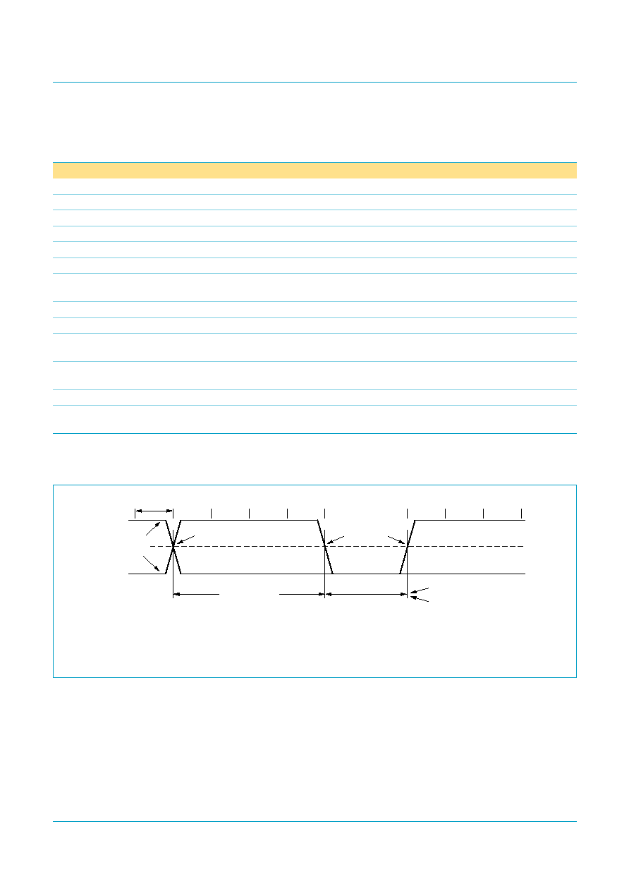
Philips Semiconductors
ISP1583
Hi-Speed USB peripheral controller
Product data
Rev. 03 -- 12 July 2004
66 of 87
9397 750 13461
© Koninklijke Philips Electronics N.V. 2004. All rights reserved.
[1]
Excluding the first transition from the idle state.
[2]
Characterized only, not tested. Limits guaranteed by design.
High-speed mode
t
HSR
high-speed differential rise time
with captive cable
500
-
-
ps
t
HSF
high-speed differential fall time
with captive cable
500
-
-
ps
Data source timing
Full-speed mode
t
FEOPT
source EOP width
see
Figure 17
[2]
160
-
175
ns
t
FDEOP
source differential data-to-EOP
transition skew
see
Figure 17
[2]
-
2
-
+5
ns
Receiver timing
Full-speed mode
t
JR1
receiver data jitter tolerance to
next transition
see
Figure 18
[2]
-
18.5
-
+18.5
ns
t
JR2
receiver data jitter tolerance for
paired transitions
see
Figure 18
[2]
-
9
-
+9
ns
t
FEOPR
receiver SE0 width
accepted as EOP; see
Figure 17
[2]
82
-
-
ns
t
FST
width of SE0 during differential
transition
rejected as EOP; see
Figure 19
[2]
-
-
14
ns
Table 100: Dynamic characteristics: analog I/O pins DP and DM
...continued
V
CC(3V3)
= 3.3 V
±
0.3 V; V
GND
= 0 V; T
amb
=
-
40
°
C to +85
°
C; C
L
= 50 pF; R
PU
= 1.5 k
on DP to V
TERM
.; test circuit of
Figure 36
; unless otherwise specified.
Symbol Parameter
Conditions
Min.
Typ
Max
Unit
T
PERIOD
is the bit duration corresponding with the USB data rate.
Full-speed timing symbols have a subscript prefix `F', low-speed timing symbols have a prefix `L'.
Fig 17. Source differential data-to-EOP transition skew and EOP width.
mgr776
T
PERIOD
differential
data lines
crossover point
differential data to
SE0/EOP skew
N
×
T
PERIOD
+
t
DEOP
source EOP width: t
EOPT
receiver EOP width: t
EOPR
crossover point
extended
+
3.3 V
0 V
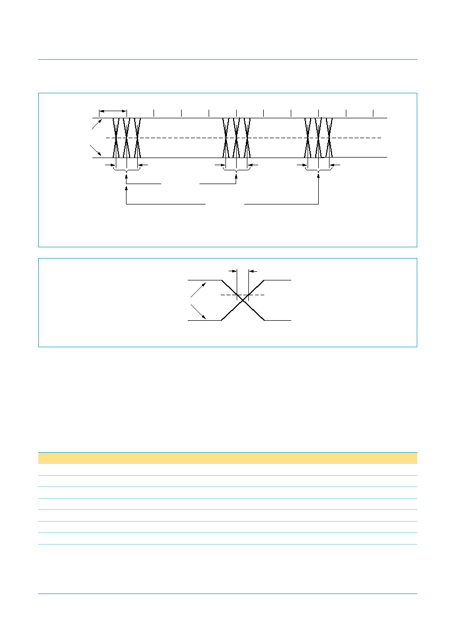
Philips Semiconductors
ISP1583
Hi-Speed USB peripheral controller
Product data
Rev. 03 -- 12 July 2004
67 of 87
9397 750 13461
© Koninklijke Philips Electronics N.V. 2004. All rights reserved.
13.1 Register access timing
13.1.1
Generic processor mode
BUS_CONF = H: generic processor mode:
·
MODE0 = H: 8051 style; see
Figure 20
·
MODE0 = L: Motorola style; see
Figure 21
.
T
PERIOD
is the bit duration corresponding with the USB data rate.
Fig 18. Receiver differential data jitter.
mgr871
T
PERIOD
t
JR
differential
data lines
+
3.3 V
0 V
t
JR1
t
JR2
consecutive
transitions
N
×
T
PERIOD
+
t
JR1
paired
transitions
N
×
T
PERIOD
+
t
JR2
Fig 19. Receiver SE0 width tolerance.
mgr872
differential
data lines
+
3.3 V
0 V
t
FST
V
IH(min)
Table 101: ISP1583 register access timing parameters: separate address and data buses
V
CC(I/O)
= 3.3 V; V
CC(3V3)
= 3.3 V; V
GND
= 0 V; T
amb
=
-
40
°
C to +85
°
C.
Symbol
Parameter
Min
Max
Unit
Reading
t
RLRH
RD_N LOW pulse width
>t
RLDV
-
ns
t
AVRL
address set-up time before RD_N LOW
0
-
ns
t
RHAX
address hold time after RD_N HIGH
0
-
ns
t
RLDV
RD_N LOW to data valid delay
-
26
ns
t
RHDZ
RD_N HIGH to data outputs 3-state delay
0
15
ns
t
RHSH
RD_N HIGH to CS_N HIGH delay
0
-
ns
t
SLRL
CS_N LOW to RD_N LOW delay
2
-
ns
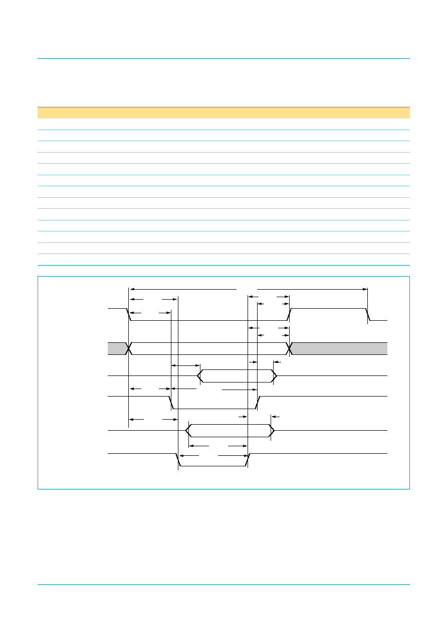
Philips Semiconductors
ISP1583
Hi-Speed USB peripheral controller
Product data
Rev. 03 -- 12 July 2004
68 of 87
9397 750 13461
© Koninklijke Philips Electronics N.V. 2004. All rights reserved.
Writing
t
WLWH
WR_N LOW pulse width
15
-
ns
t
AVWL
address set-up time before WR_N LOW
0
-
ns
t
WHAX
address hold time after WR_N HIGH
0
-
ns
t
DVWH
data set-up time before WR_N HIGH
11
-
ns
t
WHDZ
data hold time after WR_N HIGH
5
-
ns
t
WHSH
WR_N HIGH to CS_N HIGH delay
0
-
ns
t
SLWL
CS_N LOW to WR_N LOW delay
2
-
ns
General
T
cy(RW)
read/write cycle time
50
-
ns
t
I1VI2L
RW_N set-up time before DS_N LOW
0
-
ns
t
I2HI1X
RW_N hold time after DS_N HIGH
0
-
ns
t
RDY1
READY HIGH to RD_N/WR_N HIGH of the last access
-
91
ns
Table 101: ISP1583 register access timing parameters: separate address and data buses
...continued
V
CC(I/O)
= 3.3 V; V
CC(3V3)
= 3.3 V; V
GND
= 0 V; T
amb
=
-
40
°
C to +85
°
C.
Symbol
Parameter
Min
Max
Unit
Fig 20. ISP1583 register access timing: separate address and data buses (8051 style).
(write) DATA[15:0]
(read) DATA[15:0]
004aaa301
AD[7:0]
tWHSH
tAVWL
tDVWH
tRHDZ
tAVRL
Tcy(RW)
tWHAX
tRHAX
tRLDV
tWHDZ
WR_N
CS_N
RD_N
tRHSH
tRLRH
tWLWH
tSLWL
tSLRL
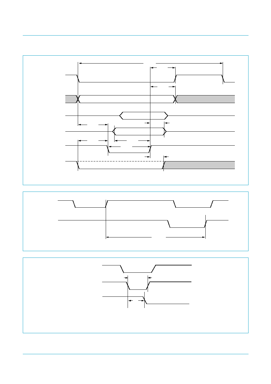
Philips Semiconductors
ISP1583
Hi-Speed USB peripheral controller
Product data
Rev. 03 -- 12 July 2004
69 of 87
9397 750 13461
© Koninklijke Philips Electronics N.V. 2004. All rights reserved.
Fig 21. ISP1583 register access timing: separate address and data buses (Motorola style).
(write) DATA[15:0]
write
(read) DATA[15:0]
read
004aaa379
AD[7:0]
tWHSH
tAVWL
tDVWH
tI1VI2L
tI2HI1X
Tcy(RW)
tWHAX
tWHDZ
RW_N
DS_N
CS_N
tWLWH
Fig 22. ISP1583 READY signal timing.
004aaa380
tRDY1
WR_N
READY
(1) Programmable polarity: shown as active LOW.
Remark: EOT should be valid for 36 ns (minimum) when RD_N/WR_N is active.
Fig 23. EOT timing in generic processor mode.
EOT
(1)
RD_N, WR_N
004aaa378
36 ns (min)
DREQ
th1

Philips Semiconductors
ISP1583
Hi-Speed USB peripheral controller
Product data
Rev. 03 -- 12 July 2004
70 of 87
9397 750 13461
© Koninklijke Philips Electronics N.V. 2004. All rights reserved.
13.1.2
Split bus mode
ALE function:
·
BUS_CONF = L: split bus mode
·
MODE1 = L: ALE function
MODE0 = H: 8051 style; see
Figure 24
MODE0 = L: Motorola style; see
Figure 25
.
Table 102: ISP1583 register access timing parameters: multiplexed address/data bus
V
CC(I/O)
= 3.3 V; V
CC(3V3)
= 3.3 V; V
GND
= 0 V; T
amb
=
-
40
°
C to +85
°
C.
Symbol
Parameter
Min
Max
Unit
Reading
t
RLRH
RD_N LOW pulse width
>t
RLDV
-
ns
t
RLDV
RD_N LOW to data valid delay
-
25
ns
t
RHDZ
RD_N HIGH to data outputs 3-state delay
0
15
ns
t
RHSH
RD_N HIGH to CS_N HIGH delay
0
-
ns
t
LLRL
ALE LOW set-up time before RD_N LOW
0
-
ns
Writing
t
WLWH
WR_N/DS_N LOW pulse width
15
-
ns
t
DVWH
data set-up time before WR_N HIGH
5
-
ns
t
LLWL
ALE LOW to WR_N/DS_N LOW delay
0
-
ns
t
WHDZ
data hold time after WR_N/DS_N HIGH
5
-
ns
t
WHSH
WR_N/DS_N HIGH to CS_N HIGH delay
0
-
ns
General
T
cy(RW)
read/write cycle time
80
-
ns
t
AVLL
address set-up time before ALE LOW
0
-
ns
t
I1VLL
RW_N set-up time before ALE LOW
5
-
ns
t
LLI2L
ALE LOW to DS_N LOW delay
5
-
ns
t
I2HI1X
RW_N hold time after DS_N HIGH
5
-
ns
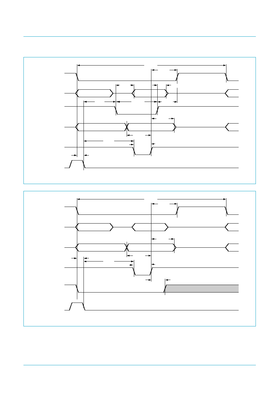
Philips Semiconductors
ISP1583
Hi-Speed USB peripheral controller
Product data
Rev. 03 -- 12 July 2004
71 of 87
9397 750 13461
© Koninklijke Philips Electronics N.V. 2004. All rights reserved.
Fig 24. ISP1583 register access timing: multiplexed address/data bus (8051 style).
address
address
data
data
(write) AD[7:0]
ALE
(read) AD[7:0]
tWHSH
tRHSH
tRHDZ
tRLDV
tLLWL
tDVWH
tLLRL
tWHDZ
tAVLL
004aaa382
Tcy(RW)
WR_N
CS_N
RD_N
tRLRH
tWLWH
Fig 25. ISP1583 register access timing: multiplexed address/data bus (Motorola style).
address
address
data
data
(write) AD[7:0]
ALE
(read) AD[7:0]
tWHSH
tLLI2L
tDVWH
tWHDZ
tI2HI1X
tI1VLL
004aaa381
Tcy(RW)
RW_N
DS_N
CS_N
tWLWH

Philips Semiconductors
ISP1583
Hi-Speed USB peripheral controller
Product data
Rev. 03 -- 12 July 2004
72 of 87
9397 750 13461
© Koninklijke Philips Electronics N.V. 2004. All rights reserved.
A0 function:
·
BUS_CONF = L: split bus mode
·
MODE1 = H: A0 function
MODE0 = H: 8051 style; see
Figure 26
MODE0 = L: Motorola style; see
Figure 27
.
Table 103: ISP1583 register access timing parameters: multiplexed address/data bus
V
CC(I/O)
= 3.3 V; V
CC(3V3)
= 3.3 V; V
GND
= 0 V; T
amb
=
-
40
°
C to +85
°
C.
Symbol
Parameter
Min
Max
Unit
Reading
t
RLDV
RD_N LOW to data valid delay
-
26
ns
t
RHDZ
RD_N HIGH to data outputs 3-state delay
0
15
ns
t
RHSH
RD_N HIGH to CS_N HIGH delay
0
-
ns
t
RLRH
RD_N LOW pulse width
>t
RLDV
-
ns
t
WHRH
WR_N/DS_N HIGH to RD_N HIGH delay
40
-
ns
Writing
t
A0WL
A0 set-up time before WR_N/DS_N LOW
0
-
ns
t
AVWH
address set-up time before WR_N/DS_N HIGH
5
-
ns
t
DVWH
data set-up time before WR_N/DS_N HIGH
5
-
ns
t
WHDZ
data hold time after WR_N/DS_N HIGH
5
-
ns
t
WHSH
WR_N/DS_N HIGH to CS_N HIGH delay
0
-
ns
t
WLWH
WR_N/DS_N LOW pulse width
15
-
ns
t
WHWH
WR_N/DS_N HIGH (address) to WR_N/DS_N HIGH (data)
delay
40
-
ns
General
T
cy(RW)
read/write cycle time
50
-
ns
t
I2HI1X
RW_N hold time after DS_N HIGH
5
-
ns
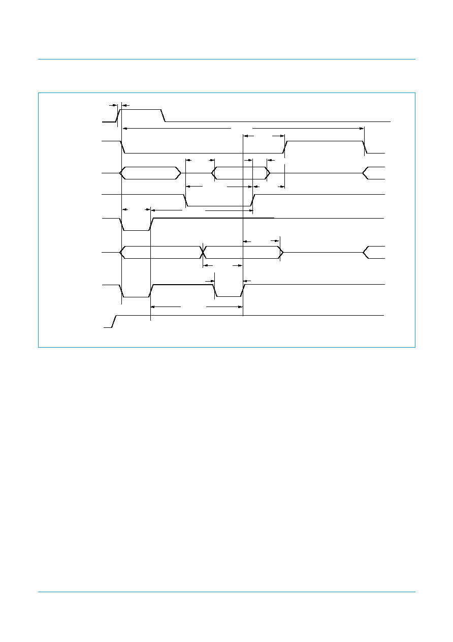
Philips Semiconductors
ISP1583
Hi-Speed USB peripheral controller
Product data
Rev. 03 -- 12 July 2004
73 of 87
9397 750 13461
© Koninklijke Philips Electronics N.V. 2004. All rights reserved.
Fig 26. ISP1583 register access timing: multiplexed address/data bus (A0 function and 8051 style).
address
address
data
data
(write) AD[7:0]
(read) AD[7:0]
tWHSH
tRHSH
tRHDZ
tRLDV
tDVWH
tWHDZ
tA0WL
004aaa383
Tcy(RW)
RD_N
WR_N
CS_N
RD_N
A0
tWHRH
tWLWH
tWHWH
tAVWH
tRLRH
WR_N
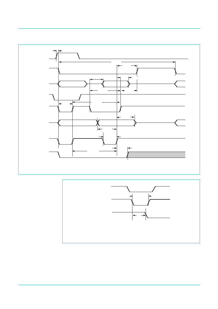
Philips Semiconductors
ISP1583
Hi-Speed USB peripheral controller
Product data
Rev. 03 -- 12 July 2004
74 of 87
9397 750 13461
© Koninklijke Philips Electronics N.V. 2004. All rights reserved.
Fig 27. ISP1583 register access timing: multiplexed address/data bus (A0 function and Motorola style).
address
address
data
data
(write) AD[7:0]
(read) AD[7:0]
tWHSH
tRHSH
tRHDZ
tRLDV
tDVWH
tWHDZ
tI2HI1X
tA0WL
004aaa384
Tcy(RW)
RW_N
DS_N
CS_N
RW_N
A0
tWHRH
tWLWH
tWHWH
tAVWH
tRLRH
DS_N
(1) Programmable polarity: shown as active LOW.
Remark: EOT should be valid for 36 ns (minimum) when DIOR/DIOW is active.
Fig 28. EOT timing in split bus mode.
EOT
(1)
DIOR/DIOW
(1)
36 ns (min)
DREQ
th1
004aaa012

Philips Semiconductors
ISP1583
Hi-Speed USB peripheral controller
Product data
Rev. 03 -- 12 July 2004
75 of 87
9397 750 13461
© Koninklijke Philips Electronics N.V. 2004. All rights reserved.
13.2 DMA timing
13.2.1
PIO mode
[1]
T
cy1
is the total cycle time, consisting of command active time t
w1
and command recovery (inactive) time t
w2
, that is, T
cy1
= t
w1
+ t
w2
. The
minimum timing requirements for T
cy1
, t
w1
and t
w2
must all be met. As T
cy1(min)
is greater than the sum of t
w1(min)
and t
w2(min)
, a host
implementation must lengthen t
w1
and/or t
w2
to ensure that T
cy1
is equal to or greater than the value reported in the IDENTIFY DEVICE
data. A device implementation shall support any legal host implementation.
[2]
t
d2
specifies the time after DIOR is negated, when the data bus is no longer driven by the device (3-state).
[3]
If IORDY is LOW at t
su4
, the host waits until IORDY is made HIGH before the PIO cycle is completed. In that case, t
su5
must be met for
reading (t
su3
does not apply). When IORDY is HIGH at t
su4
, t
su3
must be met for reading (t
su5
does not apply).
Table 104: PIO mode timing parameters
V
CC(I/O)
= 3.3 V; V
CC(3V3)
= 3.3 V; V
GND
= 0 V; T
amb
=
-
40
°
C to +85
°
C.
Symbol
Parameter
Mode 0 Mode 1 Mode 2 Mode 3 Mode 4 Unit
T
cy1(min)
read/write cycle time
[1]
600
383
240
180
120
ns
t
su1(min)
address to DIOR/DIOW on set-up time
70
50
30
30
25
ns
t
w1(min)
DIOR/DIOW pulse width
[1]
165
125
100
80
70
ns
t
w2(min)
DIOR/DIOW recovery time
[1]
-
-
-
70
25
ns
t
su2(min)
data set-up time before DIOW off
60
45
30
30
20
ns
t
h2(min)
data hold time after DIOW off
30
20
15
10
10
ns
t
su3(min)
data set-up time before DIOR on
50
35
20
20
20
ns
t
h3(min)
data hold time after DIOR off
5
5
5
5
5
ns
t
d2(max)
data to 3-state delay after DIOR off
[2]
30
30
30
30
30
ns
t
h1(min)
address hold time after DIOR/DIOW off
20
15
10
10
10
ns
t
su4(min)
IORDY after DIOR/DIOW on set-up time
[3]
35
35
35
35
35
ns
t
su5(min)
read data to IORDY HIGH set-up time
[3]
0
0
0
0
0
ns
t
w3(max)
IORDY LOW pulse width
1250
1250
1250
1250
1250
ns
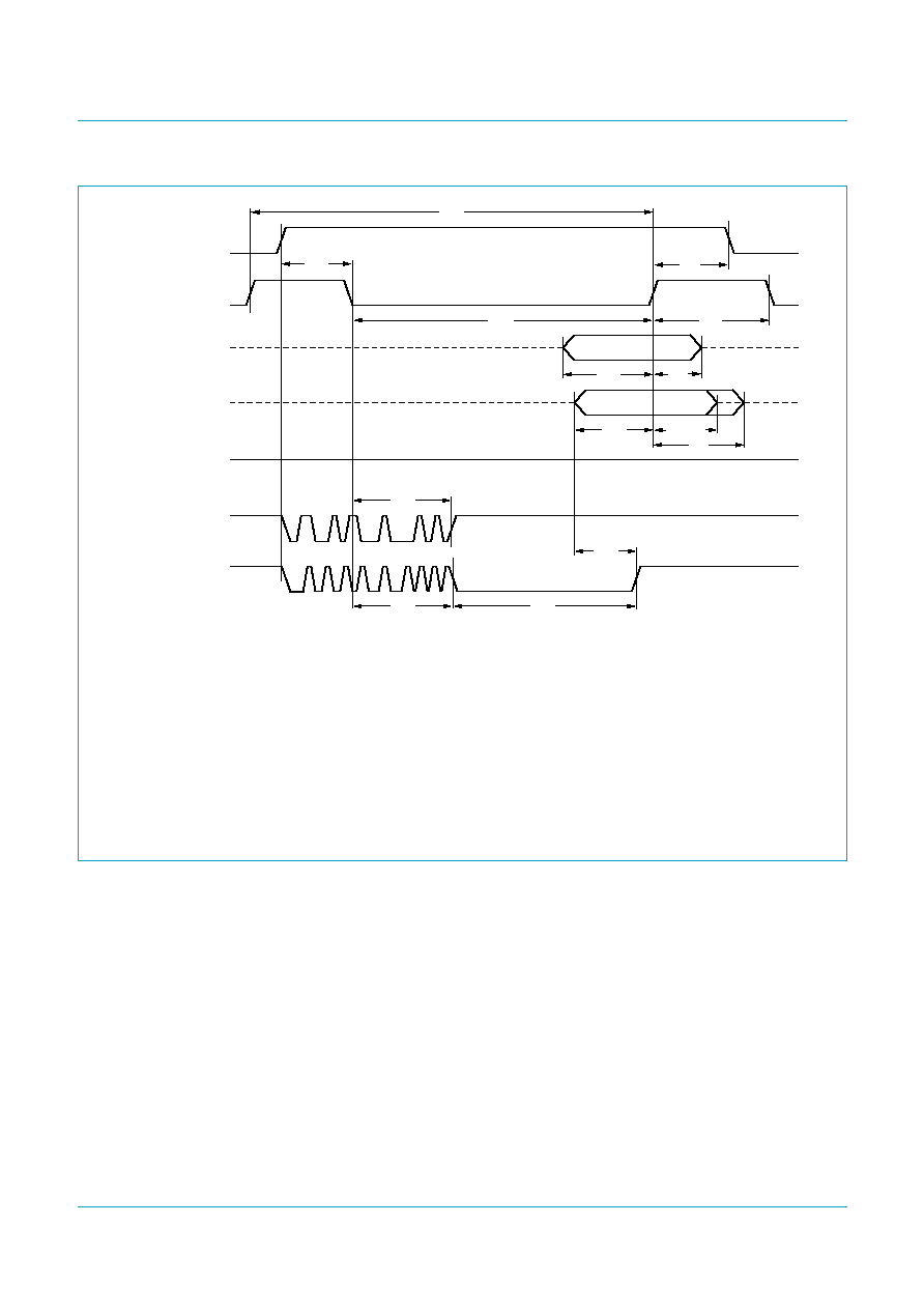
Philips Semiconductors
ISP1583
Hi-Speed USB peripheral controller
Product data
Rev. 03 -- 12 July 2004
76 of 87
9397 750 13461
© Koninklijke Philips Electronics N.V. 2004. All rights reserved.
(1) The device address consists of signals CS1_N, CS0_N, DA2, DA1 and DA0.
(2) The data bus width depends on the PIO access command used. Task File register access uses 8 bits (DATA[7:0]), except
for the Task File register 1F0 which uses 16 bits (DATA[15:0]). DMA commands 04h and 05h also use a 16-bit data bus.
(3) The device can negate IORDY to extend the PIO cycle with wait states. The host determines whether or not to extend the
current cycle after t
su4
following the assertion of DIOR or DIOW. The following three cases are distinguished:
a) Device keeps IORDY released (high-impedance): no wait state is generated.
b) Device negates IORDY during t
su4
, but re-asserts IORDY before t
su4
expires: no wait state is generated.
c) Device negates IORDY during t
su4
and keeps IORDY negated for at least 5 ns after t
su4
expires: a wait state is generated.
The cycle is completed as soon as IORDY is re-asserted. For extended read cycles (DIOR asserted), the read data on lines
DATAn must be valid at t
d1
before IORDY is asserted.
(4) DIOR and DIOW have a programmable polarity: shown here as active LOW signals.
Fig 29. PIO mode timing.
HIGH
(write) DATA[7:0]
(2)
(read) DATA[7:0]
(2)
device
(1)
address
valid
DIOR, DIOW
(4)
IORDY
(3a)
IORDY
(3b)
IORDY
(3c)
tw1
tw2
th1
tsu1
tsu2
tsu5
tsu4
tsu4
tw3
th2
tsu3
td2
th3
(min)
Tcy1
MGT499
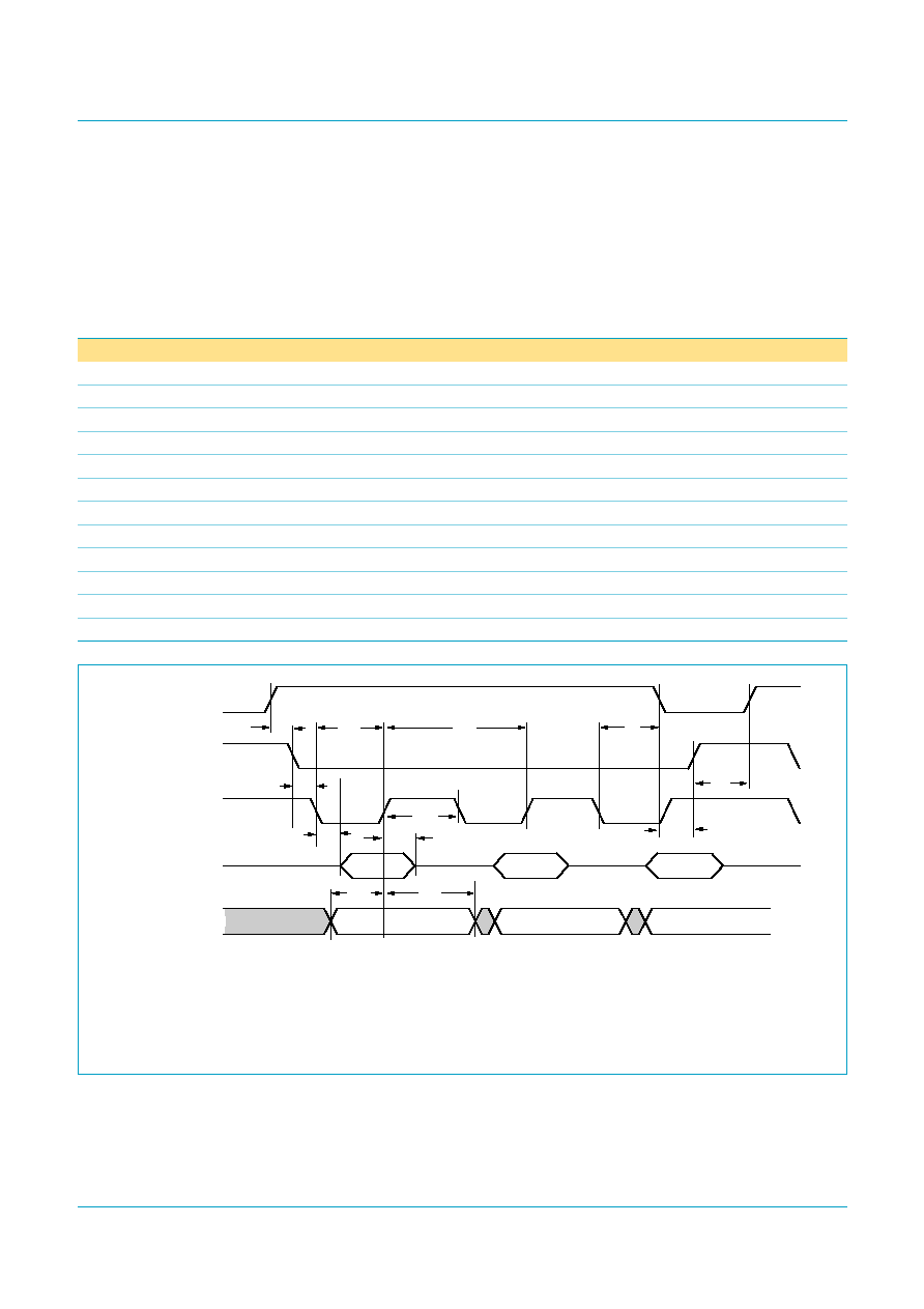
Philips Semiconductors
ISP1583
Hi-Speed USB peripheral controller
Product data
Rev. 03 -- 12 July 2004
77 of 87
9397 750 13461
© Koninklijke Philips Electronics N.V. 2004. All rights reserved.
13.2.2
GDMA slave mode
·
Bits MODE[1:0] = 00: data strobes DIOR (read) and DIOW (write); see
Figure 30
·
Bits MODE[1:0] = 01: data strobes DIOR (read) and DACK (write); see
Figure 31
·
Bits MODE[1:0] = 10: data strobes DACK (read and write); see
Figure 32
.
Table 105: GDMA slave mode timing parameters
V
CC(I/O)
= 3.3 V; V
CC(3V3)
= 3.3 V; V
GND
= 0 V; T
amb
=
-
40
°
C to +85
°
C.
Symbol
Parameter
Min
Max
Unit
T
cy1
read/write cycle time
75
-
ns
t
su1
DREQ set-up time before first DACK on
10
-
ns
t
d1
DREQ on delay after last strobe off
33.33
-
ns
t
h1
DREQ hold time after last strobe on
0
53
ns
t
w1
DIOR/DIOW pulse width
39
600
ns
t
w2
DIOR/DIOW recovery time
36
-
ns
t
d2
read data valid delay after strobe on
-
20
ns
t
h2
read data hold time after strobe off
-
5
ns
t
h3
write data hold time after strobe off
1
-
ns
t
su2
write data set-up time before strobe off
10
-
ns
t
su3
DACK setup time before DIOR/DIOW assertion
0
-
ns
t
a1
DACK deassertion after DIOR/DIOW deassertion
0
30
ns
DREQ is continuously asserted until the last transfer is done or the FIFO is full.
Data strobes: DIOR (read), DIOW (write).
(1) Programmable polarity: shown as active LOW.
(2) Programmable polarity: shown as active HIGH.
Fig 30. GDMA slave mode timing: DIOR (master) and DIOW (slave).
th1
tw1
tsu1
td1
tsu2
td2
th2
Tcy1
(write) DATA[15:0]
(read) DATA[15:0]
DREQ
(2)
DACK
(1)
DIOR/DIOW
(1)
MGT500
tsu3
tw2
ta1
th3
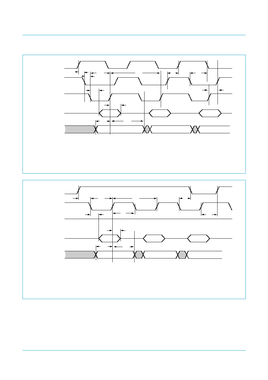
Philips Semiconductors
ISP1583
Hi-Speed USB peripheral controller
Product data
Rev. 03 -- 12 July 2004
78 of 87
9397 750 13461
© Koninklijke Philips Electronics N.V. 2004. All rights reserved.
DREQ is asserted for every transfer.
Data strobes: DIOR (read), DACK (write).
(1) Programmable polarity: shown as active LOW.
(2) Programmable polarity: shown as active HIGH.
Fig 31. GDMA slave mode timing: DIOR (master) or DACK (slave).
td1
tw1
tsu1
th1
tsu2
td2
th2
Tcy1
(write) DATA[15:0]
(read) DATA[15:0]
DREQ
(2)
DACK
(1)
DIOR/DIOW
(1)
MGT502
tsu3
ta1
th3
DREQ is continuously asserted until the last transfer is done or the FIFO is full.
Data strobe: DACK (read/write).
(1) Programmable polarity: shown as active LOW.
(2) Programmable polarity: shown as active HIGH.
Fig 32. GDMA slave mode timing: DACK (master and slave).
th1
tw1
tsu1
td1
tsu2
td2
th2
Tcy1
(write) DATA[15:0]
(read) DATA[15:0]
DREQ
(2)
HIGH
DACK
(1)
DIOR/DIOW
(1)
MGT501
tw2
th3
Philips Semiconductors
ISP1583
Hi-Speed USB peripheral controller
Product data
Rev. 03 -- 12 July 2004
79 of 87
9397 750 13461
© Koninklijke Philips Electronics N.V. 2004. All rights reserved.
13.2.3
MDMA mode
[1]
T
cy1
is the total cycle time, consisting of command active time t
w1
and command recovery (inactive) time t
w2
, that is, T
cy1
= t
w1
+ t
w2
. The
minimum timing requirements for T
cy1
, t
w1
and t
w2
must all be met. As T
cy1(min)
is greater than the sum of t
w1(min)
and t
w2(min)
, a host
implementation must lengthen t
w1
and/or t
w2
to ensure that T
cy1
is equal to or greater than the value reported in the IDENTIFY DEVICE
data. A device implementation shall support any legal host implementation.
Table 106: MDMA mode timing parameters
V
CC(I/O)
= 3.3 V; V
CC(3V3)
= 3.3 V; V
GND
= 0 V; T
amb
=
-
40
°
C to +85
°
C.
Symbol
Parameter
Mode 0
Mode 1
Mode 2
Unit
T
cy1(min)
read/write cycle time
[1]
480
150
120
ns
t
w1(min)
DIOR/DIOW pulse width
[1]
215
80
70
ns
t
d1(max)
data valid delay after DIOR on
150
60
50
ns
t
h3(min)
data hold time after DIOR off
5
5
5
ns
t
su2(min)
data set-up time before DIOR/DIOW off
100
30
20
ns
t
h2(min)
data hold time after DIOW off
20
15
10
ns
t
su1(min)
DACK set-up time before DIOR/DIOW on
0
0
0
ns
t
h1(min)
DACK hold time after DIOR/DIOW off
20
5
5
ns
t
w2(min)
DIOR recovery time)
[1]
50
50
25
ns
DIOW recovery time
[1]
215
50
25
ns
t
d2(max)
DIOR on to DREQ off delay
120
40
35
ns
DIOW on to DREQ off delay
40
40
35
ns
t
d3(max)
DACK off to data lines 3-state delay
20
25
25
ns
(1) Programmable polarity: shown as active LOW.
(2) Programmable polarity: shown as active HIGH.
Fig 33. MDMA master mode timing.
(write) DATA[15:0]
(read) DATA[15:0]
DREQ
(2)
DACK
(1)
DIOR/DIOW
(1)
tw1
tw2
tsu1
tsu2
td2
tsu2
th1
th2
th3
Tcy1
MGT506
td1
td3
Philips Semiconductors
ISP1583
Hi-Speed USB peripheral controller
Product data
Rev. 03 -- 12 July 2004
80 of 87
9397 750 13461
© Koninklijke Philips Electronics N.V. 2004. All rights reserved.
14. Application information
15. Test information
The dynamic characteristics of the analog I/O ports DP and DM were determined
using the circuit shown in
Figure 36
.
Fig 34. Typical interface connections for generic processor mode.
Fig 35. Typical interface connections for split bus mode (slave mode).
004aaa273
data
read strobe
16
ISP1583
CPU
DATA[15:0]
RW_N/RD_N
address 8
AD[7:0]
write strobe
DS_N/WR_N
chip select
CS_N
ALE/A0
8
004aaa274
DATA[15:0]
DREQ
ISP1583
DMA
8051
MICROCONTROLLER
AD[7:0]
INT
ALE/A0
P0.7/AD7
to
P0.0/AD0
ALE
DACK
DIOW
DIOR
write
strobe
read
strobe
interrupt
address
latch
enable
address/data
RW_N/RD_N
DS_N/WR_N
RD_N
INTn_N
WR_N
In full-speed mode, an internal 1.5 k
pull-up resistor is connected to pin DP.
Fig 36. Load impedance for DP and DM pins (full-speed mode).
test point
CL
50 pF
15 k
D.U.T
MGT495
Philips Semiconductors
ISP1583
Hi-Speed USB peripheral controller
Product data
Rev. 03 -- 12 July 2004
81 of 87
9397 750 13461
© Koninklijke Philips Electronics N.V. 2004. All rights reserved.
16. Package outline
Fig 37. HVQFN64 package outline.
UNIT
A
max.
A
1
D
1
A
4
b
c
e
E
h
L
e
1
y
w
v
REFERENCES
OUTLINE
VERSION
EUROPEAN
PROJECTION
ISSUE DATE
IEC
JEDEC
JEITA
mm
1
0.05
0.00
0.80
0.65
0.30
0.18
0.5
7.5
e
2
7.5
0.2
4.85
4.55
D
h
4.85
4.55
0.05
0.05
y
1
0.1
0.1
DIMENSIONS (mm are the original dimensions)
0.5
0.3
SOT804-1
- - -
MO-220
- - -
03-03-26
D
9.05
8.95
E
49
64
32
17
48
1
33
16
9.05
8.95
E
1
8.95
8.55
8.95
8.55
A
detail X
A4
A1
c
D
D1
Dh
E1 E
0
5
10 mm
scale
HVQFN64: plastic thermal enhanced very thin quad flat package; no leads; 64 terminals;
body 9 x 9 x 0.85 mm
SOT804-1
e
e
b
y
y1 C
C
B
A
A
C
C
B
v
M
w
M
e1
e2
Eh
L
terminal 1
index area
terminal 1
index area
1/2
e
1/2
e
X

Philips Semiconductors
ISP1583
Hi-Speed USB peripheral controller
Product data
Rev. 03 -- 12 July 2004
82 of 87
9397 750 13461
© Koninklijke Philips Electronics N.V. 2004. All rights reserved.
17. Soldering
17.1 Introduction to soldering surface mount packages
This text gives a very brief insight to a complex technology. A more in-depth account
of soldering ICs can be found in our
Data Handbook IC26; Integrated Circuit
Packages (document order number 9398 652 90011).
There is no soldering method that is ideal for all surface mount IC packages. Wave
soldering can still be used for certain surface mount ICs, but it is not suitable for fine
pitch SMDs. In these situations reflow soldering is recommended. In these situations
reflow soldering is recommended.
17.2 Reflow soldering
Reflow soldering requires solder paste (a suspension of fine solder particles, flux and
binding agent) to be applied to the printed-circuit board by screen printing, stencilling
or pressure-syringe dispensing before package placement. Driven by legislation and
environmental forces the worldwide use of lead-free solder pastes is increasing.
Several methods exist for reflowing; for example, convection or convection/infrared
heating in a conveyor type oven. Throughput times (preheating, soldering and
cooling) vary between 100 and 200 seconds depending on heating method.
Typical reflow peak temperatures range from 215 to 270
°
C depending on solder
paste material. The top-surface temperature of the packages should preferably be
kept:
·
below 225
°
C (SnPb process) or below 245
°
C (Pb-free process)
for all BGA, HTSSON..T and SSOP..T packages
for packages with a thickness
2.5 mm
for packages with a thickness < 2.5 mm and a volume
350 mm
3
so called
thick/large packages.
·
below 240
°
C (SnPb process) or below 260
°
C (Pb-free process) for packages with
a thickness < 2.5 mm and a volume < 350 mm
3
so called small/thin packages.
Moisture sensitivity precautions, as indicated on packing, must be respected at all
times.
17.3 Wave soldering
Conventional single wave soldering is not recommended for surface mount devices
(SMDs) or printed-circuit boards with a high component density, as solder bridging
and non-wetting can present major problems.
To overcome these problems the double-wave soldering method was specifically
developed.
If wave soldering is used the following conditions must be observed for optimal
results:
·
Use a double-wave soldering method comprising a turbulent wave with high
upward pressure followed by a smooth laminar wave.

Philips Semiconductors
ISP1583
Hi-Speed USB peripheral controller
Product data
Rev. 03 -- 12 July 2004
83 of 87
9397 750 13461
© Koninklijke Philips Electronics N.V. 2004. All rights reserved.
·
For packages with leads on two sides and a pitch (e):
larger than or equal to 1.27 mm, the footprint longitudinal axis is preferred to be
parallel to the transport direction of the printed-circuit board;
smaller than 1.27 mm, the footprint longitudinal axis must be parallel to the
transport direction of the printed-circuit board.
The footprint must incorporate solder thieves at the downstream end.
·
For packages with leads on four sides, the footprint must be placed at a 45
°
angle
to the transport direction of the printed-circuit board. The footprint must
incorporate solder thieves downstream and at the side corners.
During placement and before soldering, the package must be fixed with a droplet of
adhesive. The adhesive can be applied by screen printing, pin transfer or syringe
dispensing. The package can be soldered after the adhesive is cured.
Typical dwell time of the leads in the wave ranges from 3 to 4 seconds at 250
°
C or
265
°
C, depending on solder material applied, SnPb or Pb-free respectively.
A mildly-activated flux will eliminate the need for removal of corrosive residues in
most applications.
17.4 Manual soldering
Fix the component by first soldering two diagonally-opposite end leads. Use a low
voltage (24 V or less) soldering iron applied to the flat part of the lead. Contact time
must be limited to 10 seconds at up to 300
°
C.
When using a dedicated tool, all other leads can be soldered in one operation within
2 to 5 seconds between 270 and 320
°
C.
17.5 Package related soldering information
[1]
For more detailed information on the BGA packages refer to the
(LF)BGA Application Note
(AN01026); order a copy from your Philips Semiconductors sales office.
[2]
All surface mount (SMD) packages are moisture sensitive. Depending upon the moisture content, the
maximum temperature (with respect to time) and body size of the package, there is a risk that internal
or external package cracks may occur due to vaporization of the moisture in them (the so called
popcorn effect). For details, refer to the Drypack information in the
Data Handbook IC26; Integrated
Circuit Packages; Section: Packing Methods.
Table 107: Suitability of surface mount IC packages for wave and reflow soldering
methods
Package
[1]
Soldering method
Wave
Reflow
[2]
BGA, HTSSON..T
[3]
, LBGA, LFBGA, SQFP,
SSOP..T
[3]
, TFBGA, USON, VFBGA
not suitable
suitable
DHVQFN, HBCC, HBGA, HLQFP, HSO, HSOP,
HSQFP, HSSON, HTQFP, HTSSOP, HVQFN,
HVSON, SMS
not suitable
[4]
suitable
PLCC
[5]
, SO, SOJ
suitable
suitable
LQFP, QFP, TQFP
not recommended
[5][6]
suitable
SSOP, TSSOP, VSO, VSSOP
not recommended
[7]
suitable
CWQCCN..L
[8]
, PMFP
[9]
, WQCCN..L
[8]
not suitable
not suitable

Philips Semiconductors
ISP1583
Hi-Speed USB peripheral controller
Product data
Rev. 03 -- 12 July 2004
84 of 87
9397 750 13461
© Koninklijke Philips Electronics N.V. 2004. All rights reserved.
[3]
These transparent plastic packages are extremely sensitive to reflow soldering conditions and must
on no account be processed through more than one soldering cycle or subjected to infrared reflow
soldering with peak temperature exceeding 217
°
C
±
10
°
C measured in the atmosphere of the reflow
oven. The package body peak temperature must be kept as low as possible.
[4]
These packages are not suitable for wave soldering. On versions with the heatsink on the bottom
side, the solder cannot penetrate between the printed-circuit board and the heatsink. On versions with
the heatsink on the top side, the solder might be deposited on the heatsink surface.
[5]
If wave soldering is considered, then the package must be placed at a 45
°
angle to the solder wave
direction. The package footprint must incorporate solder thieves downstream and at the side corners.
[6]
Wave soldering is suitable for LQFP, QFP and TQFP packages with a pitch (e) larger than 0.8 mm; it
is definitely not suitable for packages with a pitch (e) equal to or smaller than 0.65 mm.
[7]
Wave soldering is suitable for SSOP, TSSOP, VSO and VSOP packages with a pitch (e) equal to or
larger than 0.65 mm; it is definitely not suitable for packages with a pitch (e) equal to or smaller than
0.5 mm.
[8]
Image sensor packages in principle should not be soldered. They are mounted in sockets or delivered
pre-mounted on flex foil. However, the image sensor package can be mounted by the client on a flex
foil by using a hot bar soldering process. The appropriate soldering profile can be provided on
request.
[9]
Hot bar soldering or manual soldering is suitable for PMFP packages.

Philips Semiconductors
ISP1583
Hi-Speed USB peripheral controller
Product data
Rev. 03 -- 12 July 2004
85 of 87
9397 750 13461
© Koninklijke Philips Electronics N.V. 2004. All rights reserved.
18. Revision history
Table 108: Revision history
Rev Date
CPCN
Description
03
20040712
-
Product data (9397 750 13461)
·
Removed Jaz
®
·
Figure 1 "Block diagram."
: added 3.3 V to the RPU line
·
Table 2 "Pin description"
: updated description for pins 8, 10, 11, 12 and 63
·
Section 8.8 "SoftConnect"
: added the second paragraph
·
Table 4 "ISP1583 pin status
[1]
"
: updated DREQ
·
Table 18 "Register overview"
: removed loopback mode in description of Fast Mode
register
·
Section 9.3.5 "Buffer Status register (address: 1Eh)"
: updated the first paragraph and
added a remark
·
Table 55 "DMA Configuration register: bit description
[1]
"
: added table note 1
·
Table 99 "Dynamic characteristics"
: added V
IN
·
Table 104 "PIO mode timing parameters"
: updated table note 1
·
Table 106 "MDMA mode timing parameters"
: updated table note 1.
02
20040503
-
Product data (9397 750 12978)
01
20040225
-
Preliminary data (9397 750 11497)

9397 750 13461
Philips Semiconductors
ISP1583
Hi-Speed USB peripheral controller
© Koninklijke Philips Electronics N.V. 2004. All rights reserved.
Product data
Rev. 03 -- 12 July 2004
86 of 87
Contact information
For additional information, please visit http://www.semiconductors.philips.com.
For sales office addresses, send e-mail to: sales.addresses@www.semiconductors.philips.com.
Fax: +31 40 27 24825
19. Data sheet status
[1]
Please consult the most recently issued data sheet before initiating or completing a design.
[2]
The product status of the device(s) described in this data sheet may have changed since this data sheet was published. The latest information is available on the Internet at
URL http://www.semiconductors.philips.com.
[3]
For data sheets describing multiple type numbers, the highest-level product status determines the data sheet status.
20. Definitions
Short-form specification -- The data in a short-form specification is
extracted from a full data sheet with the same type number and title. For
detailed information see the relevant data sheet or data handbook.
Limiting values definition -- Limiting values given are in accordance with
the Absolute Maximum Rating System (IEC 60134). Stress above one or
more of the limiting values may cause permanent damage to the device.
These are stress ratings only and operation of the device at these or at any
other conditions above those given in the Characteristics sections of the
specification is not implied. Exposure to limiting values for extended periods
may affect device reliability.
Application information -- Applications that are described herein for any
of these products are for illustrative purposes only. Philips Semiconductors
make no representation or warranty that such applications will be suitable for
the specified use without further testing or modification.
21. Disclaimers
Life support -- These products are not designed for use in life support
appliances, devices, or systems where malfunction of these products can
reasonably be expected to result in personal injury. Philips Semiconductors
customers using or selling these products for use in such applications do so
at their own risk and agree to fully indemnify Philips Semiconductors for any
damages resulting from such application.
Right to make changes -- Philips Semiconductors reserves the right to
make changes in the products - including circuits, standard cells, and/or
software - described or contained herein in order to improve design and/or
performance. When the product is in full production (status `Production'),
relevant changes will be communicated via a Customer Product/Process
Change Notification (CPCN). Philips Semiconductors assumes no
responsibility or liability for the use of any of these products, conveys no
licence or title under any patent, copyright, or mask work right to these
products, and makes no representations or warranties that these products are
free from patent, copyright, or mask work right infringement, unless otherwise
specified.
22. Trademarks
ACPI -- is an open industry specification for PC power management,
co-developed by Intel Corp., Microsoft Corp. and Toshiba
OnNow -- is a trademark of Microsoft Corp.
SoftConnect -- is a trademark of Koninklijke Philips Electronics N.V.
Zip -- is a registered trademark of Iomega Corp.
Level
Data sheet status
[1]
Product status
[2][3]
Definition
I
Objective data
Development
This data sheet contains data from the objective specification for product development. Philips
Semiconductors reserves the right to change the specification in any manner without notice.
II
Preliminary data
Qualification
This data sheet contains data from the preliminary specification. Supplementary data will be published
at a later date. Philips Semiconductors reserves the right to change the specification without notice, in
order to improve the design and supply the best possible product.
III
Product data
Production
This data sheet contains data from the product specification. Philips Semiconductors reserves the
right to make changes at any time in order to improve the design, manufacturing and supply. Relevant
changes will be communicated via a Customer Product/Process Change Notification (CPCN).

© Koninklijke Philips Electronics N.V. 2004.
Printed in The Netherlands
All rights are reserved. Reproduction in whole or in part is prohibited without the prior
written consent of the copyright owner.
The information presented in this document does not form part of any quotation or
contract, is believed to be accurate and reliable and may be changed without notice. No
liability will be accepted by the publisher for any consequence of its use. Publication
thereof does not convey nor imply any license under patent- or other industrial or
intellectual property rights.
Date of release: 12 July 2004
Document order number: 9397 750 13461
Contents
Philips Semiconductors
ISP1583
Hi-Speed USB peripheral controller
1
General description . . . . . . . . . . . . . . . . . . . . . . . . . . . 1
2
Features . . . . . . . . . . . . . . . . . . . . . . . . . . . . . . . . . . . . 2
3
Applications . . . . . . . . . . . . . . . . . . . . . . . . . . . . . . . . . 2
4
Abbreviations. . . . . . . . . . . . . . . . . . . . . . . . . . . . . . . . 3
5
Ordering information . . . . . . . . . . . . . . . . . . . . . . . . . . 3
6
Block diagram . . . . . . . . . . . . . . . . . . . . . . . . . . . . . . . 4
7
Pinning information. . . . . . . . . . . . . . . . . . . . . . . . . . . 5
7.1
Pinning . . . . . . . . . . . . . . . . . . . . . . . . . . . . . . . . . . . . 5
7.2
Pin description . . . . . . . . . . . . . . . . . . . . . . . . . . . . . . 6
8
Functional description . . . . . . . . . . . . . . . . . . . . . . . 12
8.1
DMA interface, DMA handler and DMA registers. . . 13
8.2
Hi-Speed USB transceiver . . . . . . . . . . . . . . . . . . . . 13
8.3
MMU and integrated RAM . . . . . . . . . . . . . . . . . . . . 13
8.4
Microcontroller interface and microcontroller handler 14
8.5
OTG SRP module . . . . . . . . . . . . . . . . . . . . . . . . . . 14
8.6
Philips high-speed transceiver . . . . . . . . . . . . . . . . . 14
8.6.1
Philips Parallel Interface Engine (PIE) . . . . . . . . . . . 14
8.6.2
Peripheral circuit. . . . . . . . . . . . . . . . . . . . . . . . . . . . 14
8.6.3
HS detection. . . . . . . . . . . . . . . . . . . . . . . . . . . . . . . 15
8.7
Philips Serial Interface Engine (SIE) . . . . . . . . . . . . 15
8.8
SoftConnect . . . . . . . . . . . . . . . . . . . . . . . . . . . . . . . 15
8.9
System controller . . . . . . . . . . . . . . . . . . . . . . . . . . . 15
8.10
Modes of operation . . . . . . . . . . . . . . . . . . . . . . . . . 15
8.11
Output pins status . . . . . . . . . . . . . . . . . . . . . . . . . . 16
8.12
Interrupt . . . . . . . . . . . . . . . . . . . . . . . . . . . . . . . . . . 16
8.12.1
Interrupt output pin . . . . . . . . . . . . . . . . . . . . . . . . . . 16
8.12.2
Interrupt control . . . . . . . . . . . . . . . . . . . . . . . . . . . . 17
8.13
V
BUS
sensing . . . . . . . . . . . . . . . . . . . . . . . . . . . . . . 19
8.14
Power-on reset . . . . . . . . . . . . . . . . . . . . . . . . . . . . . 20
8.15
Power supply . . . . . . . . . . . . . . . . . . . . . . . . . . . . . . 20
8.15.1
Power-sharing mode . . . . . . . . . . . . . . . . . . . . . . . . 22
8.15.2
Self-powered mode . . . . . . . . . . . . . . . . . . . . . . . . . 24
8.15.3
Bus-powered mode . . . . . . . . . . . . . . . . . . . . . . . . . 25
9
Register description . . . . . . . . . . . . . . . . . . . . . . . . . 27
9.1
Register access . . . . . . . . . . . . . . . . . . . . . . . . . . . . 28
9.2
Initialization registers . . . . . . . . . . . . . . . . . . . . . . . . 29
9.2.1
Address register (address: 00h). . . . . . . . . . . . . . . . 29
9.2.2
Mode register (address: 0Ch) . . . . . . . . . . . . . . . . . 29
9.2.3
Interrupt Configuration register (address: 10h) . . . . 32
9.2.4
OTG register (address: 12h) . . . . . . . . . . . . . . . . . . 32
9.2.5
Interrupt Enable register (address: 14h) . . . . . . . . . 34
9.3
Data flow registers . . . . . . . . . . . . . . . . . . . . . . . . . . 36
9.3.1
Endpoint Index register (address: 2Ch) . . . . . . . . . . 36
9.3.2
Control Function register (address: 28h) . . . . . . . . . 37
9.3.3
Data Port register (address: 20h). . . . . . . . . . . . . . . 38
9.3.4
Buffer Length register (address: 1Ch) . . . . . . . . . . . 39
9.3.5
Buffer Status register (address: 1Eh) . . . . . . . . . . . . 40
9.3.6
Endpoint MaxPacketSize register (address: 04h) . . 41
9.3.7
Endpoint Type register (address: 08h) . . . . . . . . . . . 42
9.4
DMA registers . . . . . . . . . . . . . . . . . . . . . . . . . . . . . 43
9.4.1
DMA Command register (address: 30h) . . . . . . . . . 44
9.4.2
DMA Transfer Counter register (address: 34h) . . . . 46
9.4.3
DMA Configuration register (address: 38h) . . . . . . . 47
9.4.4
DMA Hardware register (address: 3Ch) . . . . . . . . . . 49
9.4.5
Task File registers (addresses: 40h to 4Fh) . . . . . . . 50
9.4.6
DMA Interrupt Reason register (address: 50h). . . . . 53
9.4.7
DMA Interrupt Enable register (address: 54h) . . . . . 55
9.4.8
DMA Endpoint register (address: 58h) . . . . . . . . . . . 56
9.4.9
DMA Strobe Timing register (address: 60h) . . . . . . . 56
9.4.10
DMA Burst Counter register (address: 64h) . . . . . . . 57
9.5
General registers . . . . . . . . . . . . . . . . . . . . . . . . . . . 57
9.5.1
Interrupt register (address: 18h) . . . . . . . . . . . . . . . . 57
9.5.2
Chip ID register (address: 70h) . . . . . . . . . . . . . . . . 59
9.5.3
Frame Number register (address: 74h). . . . . . . . . . . 60
9.5.4
Scratch register (address: 78h) . . . . . . . . . . . . . . . . 60
9.5.5
Unlock Device register (address: 7Ch) . . . . . . . . . . . 61
9.5.6
Test Mode register (address: 84h) . . . . . . . . . . . . . . 62
10
Limiting values . . . . . . . . . . . . . . . . . . . . . . . . . . . . . . 63
11
Recommended operating conditions . . . . . . . . . . . . 63
12
Static characteristics . . . . . . . . . . . . . . . . . . . . . . . . . 63
13
Dynamic characteristics . . . . . . . . . . . . . . . . . . . . . . 65
13.1
Register access timing . . . . . . . . . . . . . . . . . . . . . . . 67
13.1.1
Generic processor mode . . . . . . . . . . . . . . . . . . . . . 67
13.1.2
Split bus mode . . . . . . . . . . . . . . . . . . . . . . . . . . . . . 70
13.2
DMA timing . . . . . . . . . . . . . . . . . . . . . . . . . . . . . . . . 75
13.2.1
PIO mode . . . . . . . . . . . . . . . . . . . . . . . . . . . . . . . . . 75
13.2.2
GDMA slave mode . . . . . . . . . . . . . . . . . . . . . . . . . . 77
13.2.3
MDMA mode. . . . . . . . . . . . . . . . . . . . . . . . . . . . . . . 79
14
Application information . . . . . . . . . . . . . . . . . . . . . . . 80
15
Test information . . . . . . . . . . . . . . . . . . . . . . . . . . . . . 80
16
Package outline . . . . . . . . . . . . . . . . . . . . . . . . . . . . . 81
17
Soldering. . . . . . . . . . . . . . . . . . . . . . . . . . . . . . . . . . . 82
17.1
Introduction to soldering surface mount packages . . 82
17.2
Reflow soldering . . . . . . . . . . . . . . . . . . . . . . . . . . . . 82
17.3
Wave soldering . . . . . . . . . . . . . . . . . . . . . . . . . . . . . 82
17.4
Manual soldering . . . . . . . . . . . . . . . . . . . . . . . . . . . 83
17.5
Package related soldering information . . . . . . . . . . . 83
18
Revision history . . . . . . . . . . . . . . . . . . . . . . . . . . . . . 85
19
Data sheet status . . . . . . . . . . . . . . . . . . . . . . . . . . . . 86
20
Definitions. . . . . . . . . . . . . . . . . . . . . . . . . . . . . . . . . . 86
21
Disclaimers . . . . . . . . . . . . . . . . . . . . . . . . . . . . . . . . . 86
22
Trademarks . . . . . . . . . . . . . . . . . . . . . . . . . . . . . . . . . 86
Document Outline