Äîêóìåíòàöèÿ è îïèñàíèÿ www.docs.chipfind.ru

ISP1161A1
Universal Serial Bus single-chip host and device controller
Rev. 03 -- 23 December 2004
Product data
1.
General description
The ISP1161A1 is a single-chip Universal Serial Bus (USB) Host Controller (HC) and
Device Controller (DC). The Host Controller portion of the ISP1161A1 complies with
Universal Serial Bus Specification Rev. 2.0, supporting data transfer at full-speed
(12 Mbit/s) and low-speed (1.5 Mbit/s). The Device Controller portion of the
ISP1161A1 also complies with
Universal Serial Bus Specification Rev. 2.0,
supporting data transfer at full-speed (12 Mbit/s). These two USB controllers, the HC
and the DC, share the same microprocessor bus interface. They have the same data
bus, but different I/O locations. They also have separate interrupt request output pins,
separate DMA channels that include separate DMA request output pins and DMA
acknowledge input pins. This makes it possible for a microprocessor to control both
the USB HC and the USB DC at the same time.
The ISP1161A1 provides two downstream ports for the USB HC and one upstream
port for the USB DC. Each downstream port has an overcurrent (OC) detection input
pin and power supply switching control output pin. The upstream port has a V
BUS
detection input pin.The ISP1161A1 also provides separate wake-up input pins and
suspended status output pins for the USB HC and the USB DC, respectively. This
makes power management flexible. The downstream ports for the HC can be
connected with any USB compliant devices and hubs that have USB upstream ports.
The upstream port for the DC can be connected to any USB compliant USB host and
USB hubs that have USB downstream ports.
The HC is adapted from the
Open Host Controller Interface Specification for USB
Release 1.0a, referred to as OHCI in the rest of this document.
The DC is compliant with most USB device class specifications such as Imaging
Class, Mass Storage Devices, Communication Devices, Printing Devices and Human
Interface Devices.
The ISP1161A1 is well suited for embedded systems and portable devices that
require a USB host only, a USB device only, or a combination of a configurable USB
host and USB device. The ISP1161A1 brings high flexibility to the systems that have
it built-in. For example, a system that uses an ISP1161A1 allows it not only to be
connected to a PC or USB hub with a USB downstream port, but also to be
connected to a device that has a USB upstream port such as a USB printer, USB
camera, USB keyboard or a USB mouse. Therefore, the ISP1161A1 enables
point-to-point connectivity between embedded systems. An interesting application
example is to connect an ISP1161A1 HC with an ISP1161A1 DC.
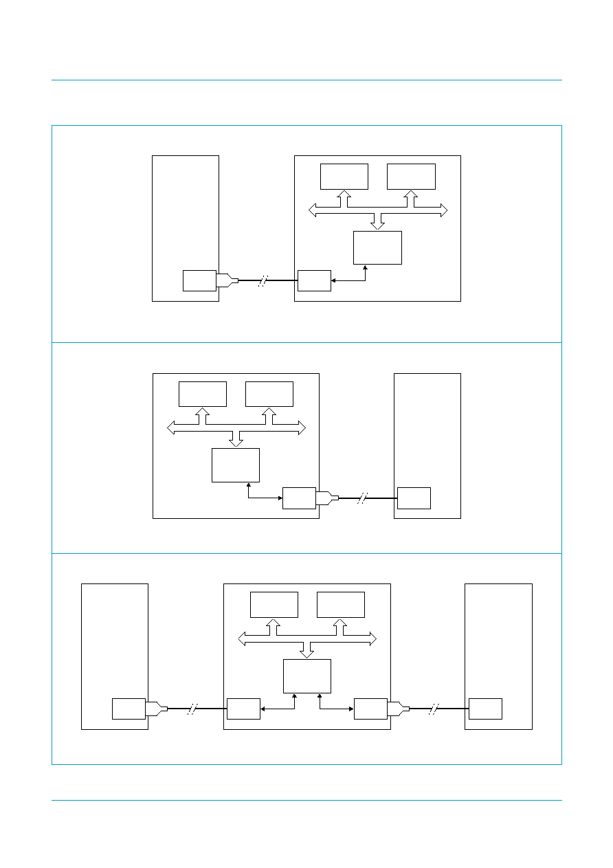
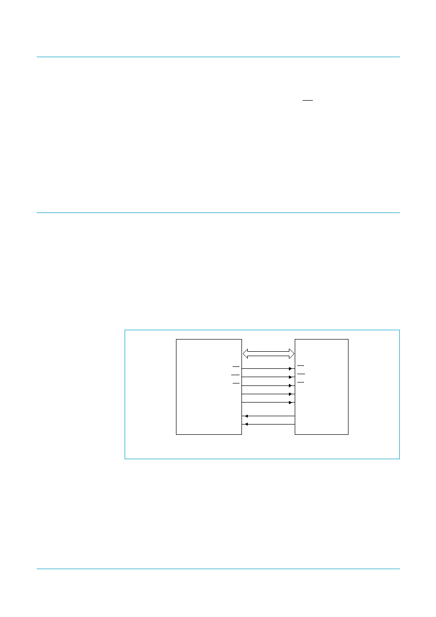
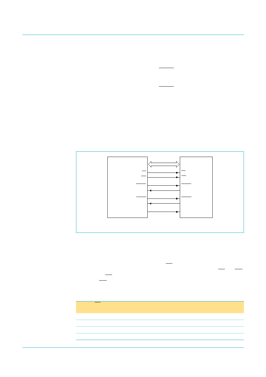
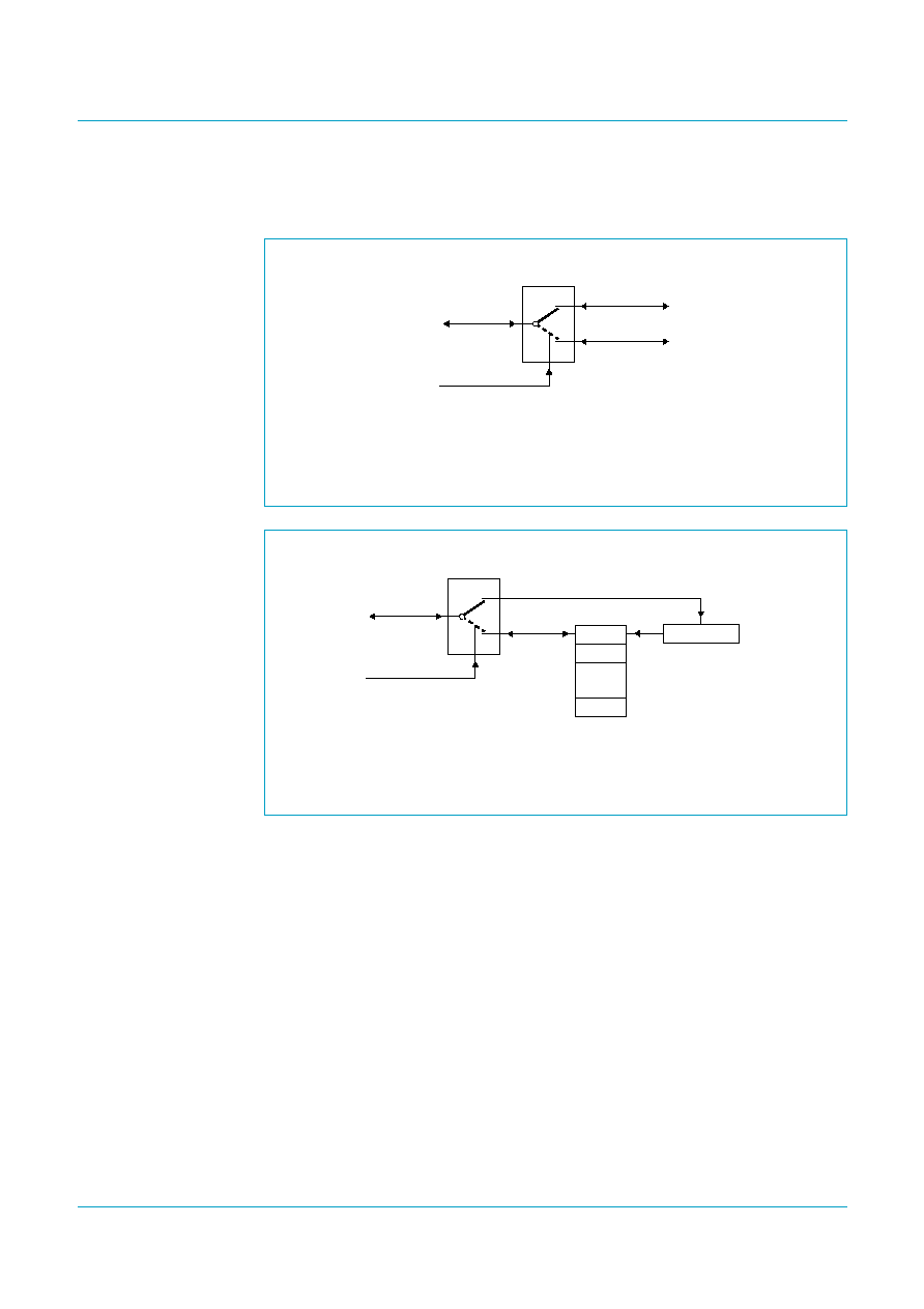
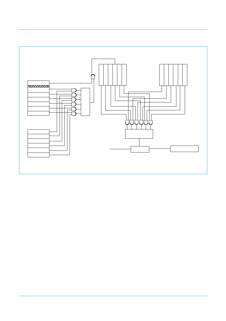
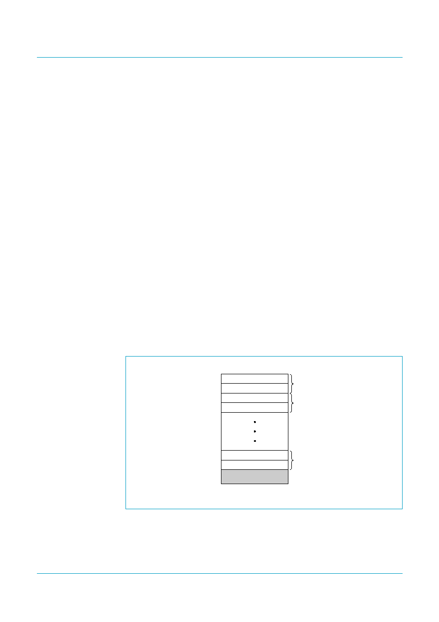
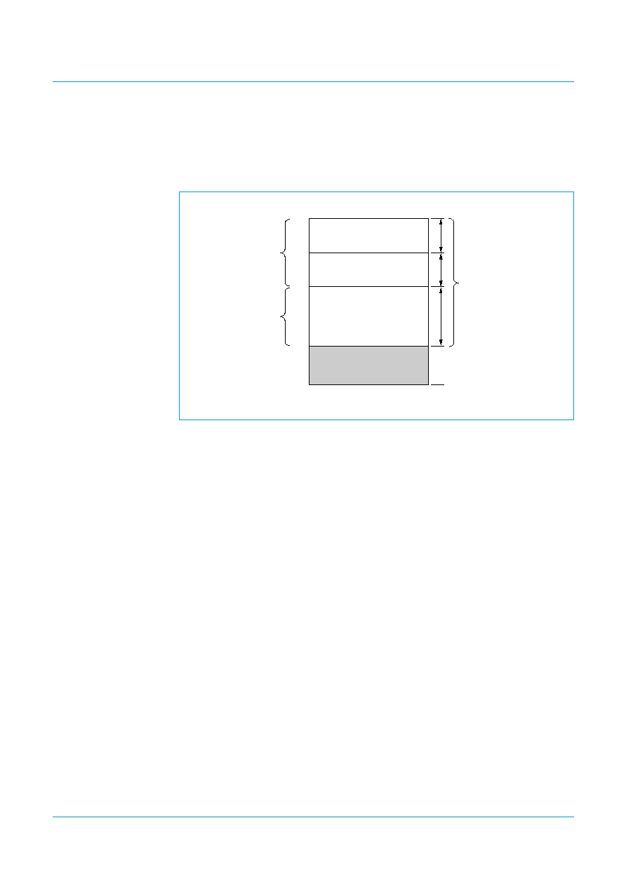
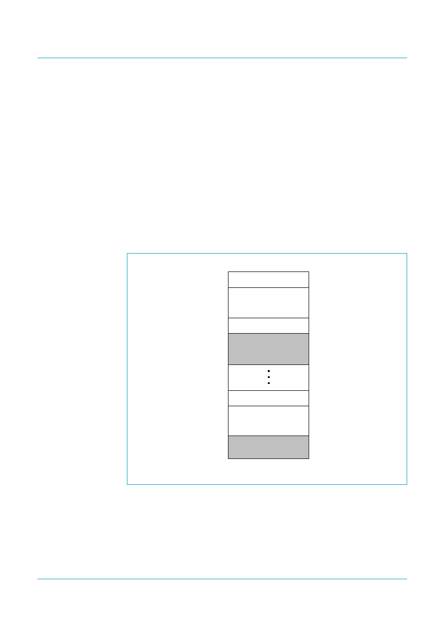
Consider an example of an ISP1161A1 being used in a Digital Still Camera (DSC)
design.
Figure 1
shows an ISP1161A1 being used as a USB DC.
Figure 2
shows an
ISP1161A1 being used as a USB HC.
Figure 3
shows an ISP1161A1 being used as a
USB HC and a USB DC at the same time.
Philips Semiconductors
ISP1161A1
USB single-chip host and device controller
Product data
Rev. 03 -- 23 December 2004
2 of 136
9397 750 13961
© Koninklijke Philips Electronics N.V. 2004. All rights reserved.
Fig 1.
ISP1161A1 operating as a USB device.
Fig 2.
ISP1161A1 operating as a stand-alone USB host.
Fig 3.
ISP1161A1 operating as both USB host and device simultaneously.
004aaa173
µ
P SYSTEM
MEMORY
µ
P
ISP1161A1
HOST/
DEVICE
µ
P bus I/F
USB I/F
USB device
USB cable
USB I/F
EMBEDDED SYSTEM
PC
(host)
DSC
004aaa174
µ
P SYSTEM
MEMORY
µ
P
ISP1161A1
HOST/
DEVICE
µ
P bus I/F
USB host
USB cable
USB I/F
EMBEDDED SYSTEM
USB I/F
PRINTER
(device)
DSC
004aaa175
µ
P SYSTEM
MEMORY
µ
P
ISP1161A1
HOST/
DEVICE
µ
P bus I/F
USB I/F
USB device
USB cable
USB cable
USB host
USB I/F
USB I/F
EMBEDDED SYSTEM
PC
(host)
USB I/F
PRINTER
(device)
DSC

Philips Semiconductors
ISP1161A1
USB single-chip host and device controller
Product data
Rev. 03 -- 23 December 2004
3 of 136
9397 750 13961
© Koninklijke Philips Electronics N.V. 2004. All rights reserved.
2.
Features
s
Complies with
Universal Serial Bus Specification Rev. 2.0
s
The Host Controller portion of the ISP1161A1 supports data transfer at full-speed
(12 Mbit/s) and low-speed (1.5 Mbit/s)
s
The Device Controller portion of the ISP1161A1 supports data transfer at
full-speed (12 Mbit/s)
s
Combines the HC and the DC in a single chip
s
On-chip DC complies with most USB device class specifications
s
Both the HC and the DC can be accessed by an external microprocessor via
separate I/O port addresses
s
Selectable one or two downstream ports for the HC and one upstream port for
the DC
s
High-speed parallel interface to most of the generic microprocessors and
Reduced Instruction Set Computer (RISC) processors such as:
x
Hitachi
®
SuperHTM SH-3 and SH-4
x
MIPS-basedTM RISC
x
ARM7TM, ARM9TM, StrongARM
®
s
Maximum 15 Mbyte/s data transfer rate between the microprocessor and the HC,
11.1 Mbyte/s data transfer rate between the microprocessor and the DC
s
Supports single-cycle and burst mode DMA operations
s
Up to 14 programmable USB endpoints with 2 fixed control IN/OUT endpoints for
the DC
s
Built-in separate FIFO buffer RAM for the HC (4 kbytes) and DC (2462 bytes)
s
Endpoints with double buffering to increase throughput and ease real-time data
transfer for both DC transfers and HC isochronous (ISO) transactions
s
6 MHz crystal oscillator with integrated PLL for low EMI
s
Controllable LazyClock (100 kHz
±
50 %) output during `suspend'
s
Clock output with programmable frequency (3 MHz to 48 MHz)
s
Software controlled connection to USB bus (SoftConnect) on upstream port for
the DC
s
Good USB connection indicator that blinks with traffic (GoodLink) for the DC
s
Software selectable internal 15 k
pull-down resistors for HC downstream ports
s
Dedicated pins for suspend sensing output and wake-up control input for flexible
applications
s
Global hardware reset input pin and separate internal software reset circuits
for HC and DC
s
Operation from a 5 V or a 3.3 V power supply
s
Operating temperature range
-
40
°
C to
+
85
°
C
s
Available in two LQFP64 packages (SOT314-2 and SOT414-1).

Philips Semiconductors
ISP1161A1
USB single-chip host and device controller
Product data
Rev. 03 -- 23 December 2004
4 of 136
9397 750 13961
© Koninklijke Philips Electronics N.V. 2004. All rights reserved.
3.
Applications
s
Personal Digital Assistant (PDA)
s
Digital camera
s
Third-generation (3-G) phone
s
Set-Top Box (STB)
s
Information Appliance (IA)
s
Photo printer
s
MP3 jukebox
s
Game console.
4.
Ordering information
Table 1:
Ordering information
Type number
Package
Name
Description
Version
ISP1161A1BD
LQFP64
plastic low profile quad flat package; 64 leads; body 10
×
10
×
1.4 mm
SOT314-2
ISP1161A1BM
LQFP64
plastic low profile quad flat package; 64 leads; body 7
×
7
×
1.4 mm
SOT414-1
xxxx xxxxxxxxxxxxxxxxxxxxxxxxxxxxxx x xxxxxxxxxxxxxx xxxxxxxxxx xxx xxxxxx xxxxxxxxxxxxxxxxxxxxxxx xxxxxxxxxxxxxxxxxxxxxx
xxxxx xxxxxx xx xxxxxxxxxxxxxxxxxxxxxxxxxxxxx xxxxxxxxxxxxxxxxxxxxxx xxxxxxxxxxx xxxxxxx xxxxxxxxxxxxxxxxxxx
xxxxxxxxxxxxxxxx xxxxxxxxxxxxxx xxxxxx xx xxxxxxxxxxxxxxxxxxxxxxxxxxxxxxxx xxxxxxxxxxxxxxxxxxxxxxxx xxxxxxx
xxxxxxxxxxxxxxxxxxxxxxxxxxxxxxxxxxxxxxxxxxxxxx xxxxxxxxxxx xxxxx x x
Philips Semiconductor
s
ISP1161A1
USB single-c
hip host and de
vice contr
oller
9397 750 13961
© K
oninklijk
e Philips Electronics N.V
. 2004. All r
ights reser
v
ed.
Pr
oduct data
Re
v
.
03 -- 23 December 2004
5 of 136
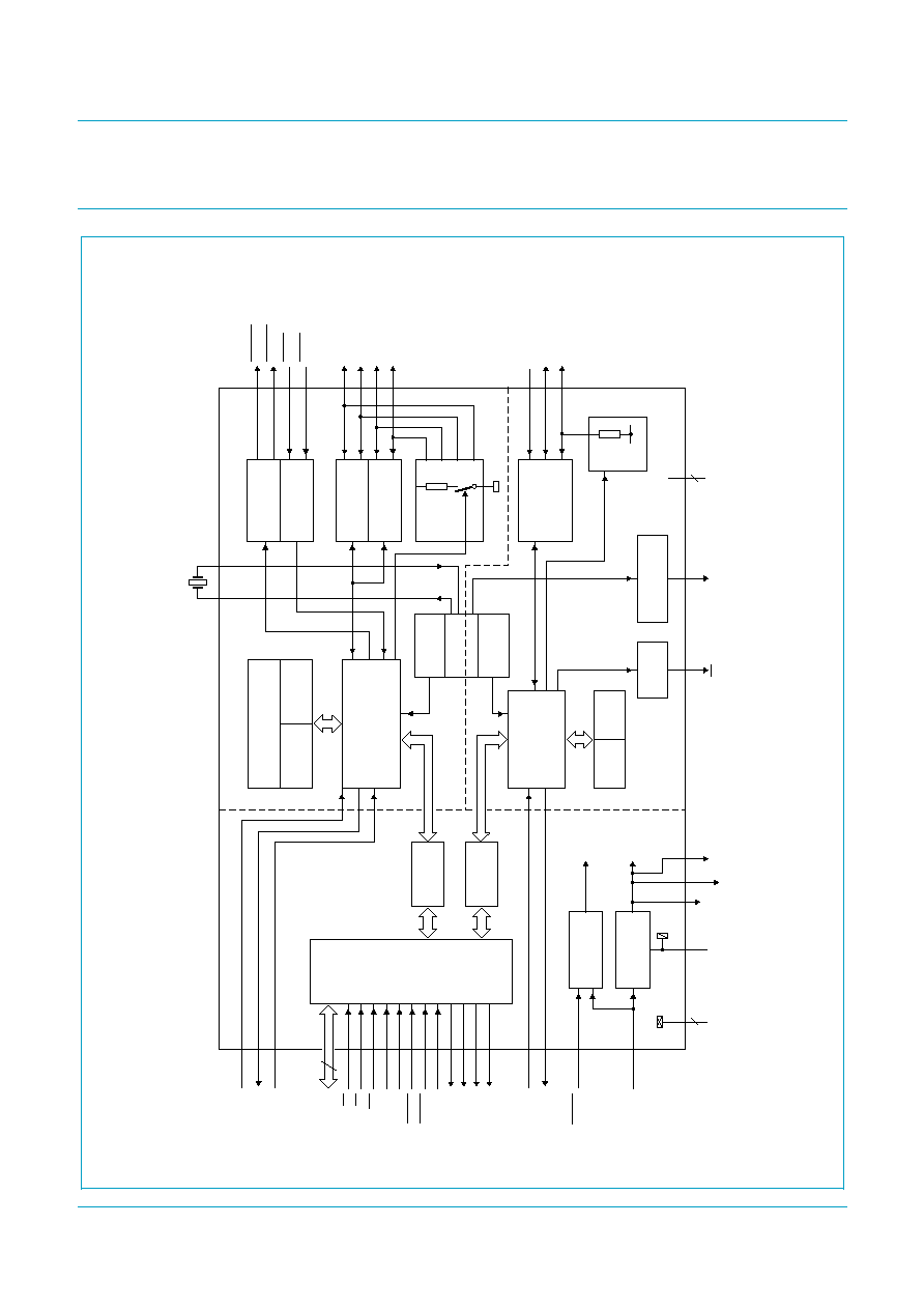
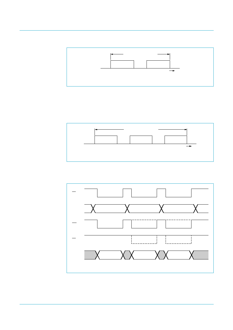
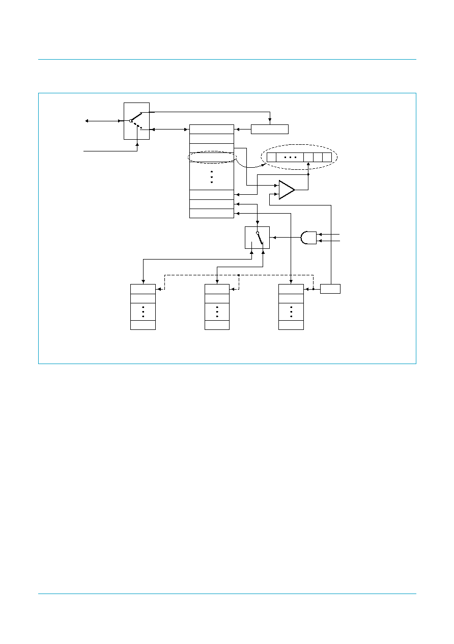
5.
Bloc
k dia
gram
Fig 4.
Block diagram.
004aaa176
16
15 k
GND
HOST/
DEVICE
AUTOMUX
HOST BUS
INTERFACE
DEVICE BUS
INTERFACE
CLOCK
RECOVERY
POWER
SWITCHING
OVERCURRENT
DETECTION
USB
TRANSCEIVER
USB
TRANSCEIVER
PLL
CLOCK
RECOVERY
GoodLink
PROGRAMMABLE
DIVIDER
HOST CONTROLLER
DEVICE
CONTROLLER
PING
RAM
PONG
RAM
VOLTAGE
REGULATOR
internal
supply
internal
reset
3.3 V
VCC
POWER-ON
RESET
Vreg(3.3)
Vhold1
DGND
GL
CLKOUT
7
1, 8, 15, 18,
35, 45, 62
2
USB
TRANSCEIVER
ITL0
(PING RAM)
ITL1
(PONG RAM)
ISP1161A1
H_WAKEUP
to/ from
microprocessor
H_PSW1
46
43
41
38
19
Vhold2
24
58
57
2 to 7,
9 to 14,
16, 17,
63, 64
40
42
33
22
21
23
60
59
28
27
34
26
25
30
29
37
36
32
56
n.c.
61, 20
44
47
54
55
50
51
52
53
39
48
49
XTAL1
XTAL2
H_PSW2
H_OC1
H_OC2
D_VBUS
DEVICE
CONTROLLER
HOST CONTROLLER
USB bus
upstream
port
USB bus
downstream
ports
H_DM1
H_DP1
H_DM2
H_DP2
D_DM
D_DP
H_SUSPEND
NDP_SEL
D0 to D15
RD
DACK2
DACK1
EOT
DREQ1
DREQ2
INT2
INT1
D_WAKEUP
D_SUSPEND
RESET
ALT RAM
6 MHz
Host bus
Device bus
4
×
1.5 k
3.3 V
SoftConnect
AGND
CS
WR
A1
A0
Philips Semiconductors
ISP1161A1
USB single-chip host and device controller
Product data
Rev. 03 -- 23 December 2004
6 of 136
9397 750 13961
© Koninklijke Philips Electronics N.V. 2004. All rights reserved.
Fig 5.
Host controller sub-block diagram.
MGT930
REGISTER
ACCESS
DMA
HANDLER
POWER-ON
RESET
ITL0 RAM
ATL RAM
ITL1 RAM
µ
P
HANDLER
PDT_LIST
PROCESS
USB
TRANSCEIVER
USB bus
H_DP1
H_DM1
H_DP2
H_DM2
PHILIPS
SIE
clock
recovery
µ
P interface
USB Interface
Philips sHC core
Memory block
Host controller sub-blocks
BUS I
/
F
Host
bus I/F
FRAME
MANAGE-
MENT
USB
STATE
MEMORY
MANAGEMENT
UNIT
Fig 6.
Device controller sub-block diagram.
MGT931
µ
P HANDLER
DMA HANDLER
POWER-ON
RESET
EP HANDLER
PHILIPS SIE
D_DP
USB bus
D_DM
USB
TRANSCEIVER
MEMORY
MANAGEMENT UNIT
INTEGRATED
RAM
BUS I/F
clock recovery
3.3 V
GoodLink
GL
SoftConnect
Device
bus I/F
Device controller sub-blocks
Philips Semiconductors
ISP1161A1
USB single-chip host and device controller
Product data
Rev. 03 -- 23 December 2004
7 of 136
9397 750 13961
© Koninklijke Philips Electronics N.V. 2004. All rights reserved.
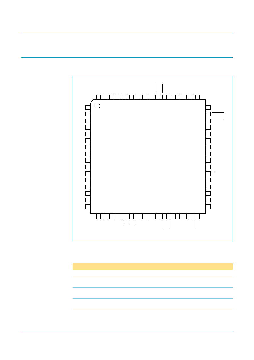
6.
Pinning information
6.1 Pinning
6.2 Pin description
Fig 7.
Pin configuration LQFP64.
ISP1161A1BD
ISP1161A1BM
004aaa177
1
2
3
4
5
6
7
8
9
10
11
12
13
14
15
16
48
47
46
45
44
43
42
41
40
39
38
37
36
35
34
D_DM
H_PSW2
H_PSW1
DGND
33
17
18
19
20
21
22
23
24
25
26
27
28
29
30
31
32
64
63
62
61
60
59
58
57
56
55
54
53
52
51
50
D1
D0
DGND
n.c.
A1
A0
V
reg(3.3)
AGND
V
CC
H_OC2
H_OC1
H_DP2
H_DM2
H_DP1
H_DM1
D_DP
49
DGND
D2
D3
D4
D5
D6
DGND
D8
D10
D11
D7
D9
D13
DGND
D14
D15
DGND
V
hold1
n.c.
RD
WR
V
hold2
D12
CS
TEST
INT2
INT1
DACK2
DACK1
DREQ2
DREQ1
RESET
D_SUSPEND
DGND
EOT
NDP_SEL
XTAL2
XTAL1
H_SUSPEND
H_WAKEUP
D_VBUS
GL
D_WAKEUP
CLKOUT
Table 2:
Pin description for LQFP64
Symbol
[1]
Pin
Type
Description
DGND
1
-
digital ground
D2
2
I/O
bit 2 of bidirectional data; slew-rate controlled; TTL input;
three-state output
D3
3
I/O
bit 3 of bidirectional data; slew-rate controlled; TTL input;
three-state output
D4
4
I/O
bit 4 of bidirectional data; slew-rate controlled; TTL input;
three-state output
D5
5
I/O
bit 5 of bidirectional data; slew-rate controlled; TTL input;
three-state output

Philips Semiconductors
ISP1161A1
USB single-chip host and device controller
Product data
Rev. 03 -- 23 December 2004
8 of 136
9397 750 13961
© Koninklijke Philips Electronics N.V. 2004. All rights reserved.
D6
6
I/O
bit 6 of bidirectional data; slew-rate controlled; TTL input;
three-state output
D7
7
I/O
bit 7 of bidirectional data; slew-rate controlled; TTL input;
three-state output
DGND
8
-
digital ground
D8
9
I/O
bit 8 of bidirectional data; slew-rate controlled; TTL input;
three-state output
D9
10
I/O
bit 9 of bidirectional data; slew-rate controlled; TTL input;
three-state output
D10
11
I/O
bit 10 of bidirectional data; slew-rate controlled; TTL input;
three-state output
D11
12
I/O
bit 11 of bidirectional data; slew-rate controlled; TTL input;
three-state output
D12
13
I/O
bit 12 of bidirectional data; slew-rate controlled; TTL input;
three-state output
D13
14
I/O
bit 13 of bidirectional data; slew-rate controlled; TTL input;
three-state output
DGND
15
-
digital ground
D14
16
I/O
bit 14 of bidirectional data; slew-rate controlled; TTL input;
three-state output
D15
17
I/O
bit 15 of bidirectional data; slew-rate controlled; TTL input;
three-state output
DGND
18
-
digital ground
V
hold1
19
-
voltage holding pin; internally connected to the V
reg(3.3)
and
V
hold2
pins. When V
CC
is connected to 5 V, this pin will
output 3.3 V, hence do not connect it to 5 V. When V
CC
is
connected to 3.3 V, this pin can either be connected to
3.3 V or left unconnected. In all cases, decouple this pin to
DGND.
n.c.
20
-
no connection
CS
21
I
chip select input
RD
22
I
read strobe input
WR
23
I
write strobe input
V
hold2
24
-
voltage holding pin; internally connected to the V
reg(3.3)
and
V
hold1
pins. When V
CC
is connected to 5 V, this pin will
output 3.3 V, hence do not connect it to 5 V. When V
CC
is
connected to 3.3 V, this pin can either be connected to
3.3 V or left unconnected. In all cases, decouple this pin to
DGND.
DREQ1
25
O
HC DMA request output (programmable polarity); signals
to the DMA controller that the ISP1161A1 wants to start a
DMA transfer; see
Section 10.4.1
DREQ2
26
O
DC DMA request output (programmable polarity); signals
to the DMA controller that the ISP1161A1 wants to start a
DMA transfer; see
Section 13.1.4
DACK1
27
I
HC DMA acknowledge input; when not in use, this pin must
be connected to V
CC
via an external 10 k
resistor
Table 2:
Pin description for LQFP64
...continued
Symbol
[1]
Pin
Type
Description

Philips Semiconductors
ISP1161A1
USB single-chip host and device controller
Product data
Rev. 03 -- 23 December 2004
9 of 136
9397 750 13961
© Koninklijke Philips Electronics N.V. 2004. All rights reserved.
DACK2
28
I
DC DMA acknowledge input; when not in use, this pin must
be connected to V
CC
via an external 10 k
resistor
INT1
29
O
HC interrupt output; programmable level, edge triggered
and polarity; see
Section 10.4.1
INT2
30
O
DC interrupt output; programmable level, edge triggered
and polarity; see
Section 13.1.4
TEST
31
O
test output; used for test purposes only; this pin is not
connected during normal operation
RESET
32
I
reset input (Schmitt trigger); a LOW level produces an
asynchronous reset (internal pull-up resistor)
NDP_SEL
33
I
indicates to the HC software the Number of Downstream
Ports (NDP) present:
0 -- select 1 downstream port
1 -- select 2 downstream ports
only changes the value of the NDP field in the
HcRhDescriptorA register; both ports will always be
enabled; see
Section 10.3.1
(internal pull-up resistor)
EOT
34
I
DMA master device to inform the ISP1161A1 of end of
DMA transfer; active level is programmable; see
Section 10.4.1
DGND
35
-
digital ground
D_SUSPEND
36
O
DC `suspend' state indicator output; active HIGH
D_WAKEUP
37
I
DC wake-up input; generates a remote wake-up from
`suspend' state (active HIGH); when not in use, this pin
must be connected to DGND via an external 10 k
resistor
(internal pull-down resistor)
GL
38
O
GoodLink LED indicator output (open-drain, 8 mA); the
LED is default ON, blinks OFF upon USB traffic; to connect
a LED use a series resistor of 470
(V
CC
= 5.0 V) or
330
(V
CC
= 3.3 V)
D_VBUS
39
I
DC USB upstream port V
BUS
sensing input; when not in
use, this pin must be connected to DGND via a 1 M
resistor
H_WAKEUP
40
I
HC wake-up input; generates a remote wake-up from
`suspend' state (active HIGH); when not in use, this pin
must be connected to DGND via an external 10 k
resistor
(internal pull-down resistor)
CLKOUT
41
O
programmable clock output (3 MHz to 48 MHz); default
12 MHz
H_SUSPEND
42
O
HC `suspend' state indicator output; active HIGH
XTAL1
43
I
crystal input; connected directly to a 6 MHz crystal; when
XTAL1 is connected to an external clock source, pin XTAL2
must be left open
XTAL2
44
O
crystal output; connected directly to a 6 MHz crystal; when
pin XTAL1 is connected to an external clock source, this
pin must be left open
Table 2:
Pin description for LQFP64
...continued
Symbol
[1]
Pin
Type
Description

Philips Semiconductors
ISP1161A1
USB single-chip host and device controller
Product data
Rev. 03 -- 23 December 2004
10 of 136
9397 750 13961
© Koninklijke Philips Electronics N.V. 2004. All rights reserved.
[1]
Symbol names with an overscore (e.g. NAME) represent active LOW signals.
DGND
45
-
digital ground
H_PSW1
46
O
power switching control output for downstream port 1;
open-drain output
H_PSW2
47
O
power switching control output for downstream port 2;
open-drain output
D_DM
48
AI/O
USB D
-
data line for DC upstream port; when not in use,
this pin must be left open
D_DP
49
AI/O
USB D+ data line for DC upstream port; when not in use,
this pin must be left open
H_DM1
50
AI/O
USB D
-
data line for HC downstream port 1
H_DP1
51
AI/O
USB D+ data line for HC downstream port 1
H_DM2
52
AI/O
USB D
-
data line for HC downstream port 2; when not in
use, this pin must be left open
H_DP2
53
AI/O
USB D+ data line for HC downstream port 2; when not in
use, this pin must be left open
H_OC1
54
I
overcurrent sensing input for HC downstream port 1
H_OC2
55
I
overcurrent sensing input for HC downstream port 2
V
CC
56
-
power supply voltage input (3.0 V to 3.6 V or
4.75 V to 5.25 V). This pin supplies the internal 3.3 V
regulator input. When connected to 5 V, the internal
regulator will output 3.3 V to pins V
reg(3.3)
, V
hold1
and V
hold2
.
When connected to 3.3 V, it will bypass the internal
regulator.
AGND
57
-
analog ground
V
reg(3.3)
58
-
internal 3.3 V regulator output; when pin V
CC
is connected
to 5 V, this pin outputs 3.3 V. When pin V
CC
is connected to
3.3 V, connect this pin to 3.3 V.
A0
59
I
address input; selects command (A0 = 1) or data (A0 = 0)
A1
60
I
address input; selects AutoMux switching to DC (A1 = 1) or
AutoMux switching to HC (A1 = 0); see
Table 3
n.c.
61
-
no connection
DGND
62
-
digital ground
D0
63
I/O
bit 0 of bidirectional data; slew-rate controlled; TTL input;
three-state output
D1
64
I/O
bit 1 of bidirectional data; slew-rate controlled; TTL input;
three-state output
Table 2:
Pin description for LQFP64
...continued
Symbol
[1]
Pin
Type
Description

Philips Semiconductors
ISP1161A1
USB single-chip host and device controller
Product data
Rev. 03 -- 23 December 2004
11 of 136
9397 750 13961
© Koninklijke Philips Electronics N.V. 2004. All rights reserved.
7.
Functional description
7.1 PLL clock multiplier
A 6 MHz to 48 MHz clock multiplier Phase-Locked Loop (PLL) is integrated on-chip.
This allows for the use of a low-cost 6 MHz crystal, which also minimizes EMI. No
external components are required for the operation of the PLL.
7.2 Bit clock recovery
The bit clock recovery circuit recovers the clock from the incoming USB data stream
using a 4 times over-sampling principle. It is able to track jitter and frequency drift as
specified in the
Universal Serial Bus Specification Rev. 2.0.
7.3 Analog transceivers
Three sets of transceivers are embedded in the chip: two are used for downstream
ports with USB connector type A; one is used for upstream port with USB connector
type B. The integrated transceivers are compliant with the
Universal Serial Bus
Specification Rev. 2.0. They interface directly with the USB connectors and cables
through external termination resistors.
7.4 Philips Serial Interface Engine (SIE)
The Philips SIE implements the full USB protocol layer. It is completely hardwired for
speed and needs no firmware intervention. The functions of this block include:
synchronization pattern recognition, parallel/serial conversion, bit (de)stuffing, CRC
checking/generation, Packet IDentifier (PID) verification/generation, address
recognition, handshake evaluation/generation. There are separate SIEs in the HC
and the DC.
7.5 SoftConnect
The connection to the USB is accomplished by bringing D
+
(for full-speed USB
devices) HIGH through a 1.5 k
pull-up resistor. In the ISP1161A1 DC, the 1.5 k
pull-up resistor is integrated on-chip and is not connected to V
CC
by default. The
connection is established through a command sent by the external/system
microcontroller. This allows the system microcontroller to complete its initialization
sequence before deciding to establish connection with the USB. Re-initialization of
the USB connection can also be performed without disconnecting the cable.
The ISP1161A1 DC will check for USB V
BUS
availability before the connection can be
established. V
BUS
sensing is provided through pin D_VBUS.
Remark: The tolerance of the internal resistors is 25 %. This is higher than the 5 %
tolerance specified by the USB specification. However, the overall voltage
specification for the connection can still be met with a good margin. The decision to
make use of this feature lies with the USB equipment designer.
Philips Semiconductors
ISP1161A1
USB single-chip host and device controller
Product data
Rev. 03 -- 23 December 2004
12 of 136
9397 750 13961
© Koninklijke Philips Electronics N.V. 2004. All rights reserved.
7.6 GoodLink
Indication of a good USB connection is provided at pin GL through GoodLink
technology. During enumeration, the LED indicator will blink on momentarily. When
the DC has been successfully enumerated (the device address is set), the LED
indicator will remain permanently on. Upon each successful packet transfer (with
ACK) to and from the ISP1161A1 the LED will blink off for 100 ms. During `suspend'
state the LED will remain off.
This feature provides a user-friendly indication of the status of the USB device, the
connected hub and the USB traffic. It is a useful field diagnostics tool for isolating
faulty equipment. It can therefore help to reduce field support and hotline overhead.
8.
Microprocessor bus interface
8.1 Programmed I/O (PIO) addressing mode
A generic PIO interface is defined for speed and ease-of-use. It also allows direct
interfacing to most microcontrollers. To a microcontroller, the ISP1161A1 appears as
a memory device with a 16-bit data bus and uses only two address lines: A1 and A0
to access the internal control registers and FIFO buffer RAM. Therefore, the
ISP1161A1 occupies only four I/O ports or four memory locations of a
microprocessor. External microprocessors can read from or write to the ISP1161A1
internal control registers and FIFO buffer RAM through the Programmed I/O (PIO)
operating mode.
Figure 8
shows the Programmed I/O interface between a
microprocessor and an ISP1161A1.
8.2 DMA mode
The ISP1161A1 also provides DMA mode for external microprocessors to access its
internal FIFO buffer RAM. Data can be transferred by DMA operation between a
microprocessor's system memory and the ISP1161A1 internal FIFO buffer RAM.
Remark: The DMA operation must be controlled by the external microprocessor
system DMA controller (Master).
Fig 8.
Programmed I/O interface between a microprocessor and an ISP1161A1.
004aaa178
D[15:0]
RD
WR
CS
A2
IRQ2
MICRO-
PROCESSOR
ISP1161A1
D[15:0]
µ
P bus I/F
RD
WR
CS
A1
A1
IRQ1
A0
INT1
INT2
Philips Semiconductors
ISP1161A1
USB single-chip host and device controller
Product data
Rev. 03 -- 23 December 2004
13 of 136
9397 750 13961
© Koninklijke Philips Electronics N.V. 2004. All rights reserved.
Figure 9
shows the DMA interface between a microprocessor system and the
ISP1161A1. The ISP1161A1 provides two DMA channels:
·
DMA channel 1 (controlled by DREQ1, DACK1 signals) is for the DMA transfer
between a microprocessor's system memory and the ISP1161A1 HC internal
FIFO buffer RAM.
·
DMA channel 2 (controlled by DREQ2, DACK2 signals) is for the DMA transfer
between a microprocessor system memory and the ISP1161A1 DC internal FIFO
buffer RAM.
The EOT signal is an external end-of-transfer signal used to terminate the DMA
transfer. Some microprocessors may not have this signal. In this case, the
ISP1161A1 provides an internal EOT signal to terminate the DMA transfer as well.
Setting the HcDMAConfiguration register (21H to read, A1H to write) enables the
ISP1161A1 HC internal DMA counter for DMA transfer. When the DMA counter
reaches the value set in the HcTransferCounter register (22H to read, A2H to write),
an internal EOT signal will be generated to terminate the DMA transfer.
8.3 Control register access by PIO mode
8.3.1
I/O port addressing
Table 3
shows the ISP1161A1 I/O port addressing. Complete decoding of the I/O port
address should include the chip select signal CS and the address lines A1 and A0.
However, the direction of the access of the I/O ports is controlled by the RD and WR
signals. When RD is LOW, the microprocessor reads data from the ISP1161A1 data
port. When WR is LOW, the microprocessor writes a command to the command port,
or writes data to the data port.
Fig 9.
DMA interface between a microprocessor and an ISP1161A1.
004aaa179
D[15:0]
RD
WR
DACK1
DREQ1
EOT
MICRO-
PROCESSOR
ISP1161A1
D[15:0]
µ
P bus I/F
RD
WR
DACK1
DREQ1
DACK2
DREQ2
DACK2
DREQ2
EOT
Table 3:
I/O port addressing
Port
CS
A1,A0
(Bin)
Access
Data bus width
(bits)
Description
0
0
00
R/W
16
HC data port
1
0
01
W
16
HC command port
2
0
10
R/W
16
DC data port
3
0
11
W
16
DC command port
Philips Semiconductors
ISP1161A1
USB single-chip host and device controller
Product data
Rev. 03 -- 23 December 2004
14 of 136
9397 750 13961
© Koninklijke Philips Electronics N.V. 2004. All rights reserved.
Figure 10
and
Figure 11
illustrate how an external microprocessor accesses the
ISP1161A1 internal control registers.
8.3.2
Register access phases
The ISP1161A1 register structure is a command-data register pair structure. A
complete register access cycle comprises a command phase followed by a data
phase. The command (also known as the index of a register) points the ISP1161A1 to
the next register to be accessed. A command is 8 bits long. On a microprocessor's
16-bit data bus, a command occupies the lower byte, with the upper byte filled with
zeros.
Figure 12
shows a complete 16-bit register access cycle for the ISP1161A1. The
microprocessor writes a command code to the command port, and then reads or
writes the data word from or to the data port. Take the example of a microprocessor
attempting to read the ISP1161A1's ID, which is saved in the HC's HcChipID register
(index 27H, read only). The 16-bit register access cycle is therefore:
1. Microprocessor writes the command code of 27H (0027H in 16-bit width) to
the HC command port
2. Microprocessor reads the data word of the chip's ID (6110H for engineering
sample; version one) from the HC data port.
When A1 = 0, the microprocessor accesses the HC.
When A1 = 1, the microprocessor accesses the DC.
Fig 10. Microprocessor access to a HC or a DC via an automux switch.
When A0 = 0, the microprocessor accesses the data port.
When A0 = 1, the microprocessor accesses the command port.
Fig 11. Microprocessor access to internal control registers.
MGT935
µ
P bus I/F
Host bus I/F
Device bus I/F
AUTOMUX
DC/HC
A1
0
1
MGT936
CMD/DATA
SWITCH
Commands
Control registers
Command register
data port
A0
command port
.
.
.
Host or Device
bus I/F
1
0
Philips Semiconductors
ISP1161A1
USB single-chip host and device controller
Product data
Rev. 03 -- 23 December 2004
15 of 136
9397 750 13961
© Koninklijke Philips Electronics N.V. 2004. All rights reserved.
Most of the ISP1161A1 internal control registers are 16-bit wide. Some of the internal
control registers, however, have 32-bit width.
Figure 13
shows how the 32-bit internal
control register is accessed. The complete cycle of accessing a 32-bit register
consists of a command phase followed by two data phases. In the two data phases,
the microprocessor first reads or writes the lower 16-bit data, followed by the upper
16-bit data.
To further describe the complete access cycles of the internal control registers, the
status of some pins of the microprocessor bus interface are shown in
Figure 14
and
Figure 15
for the HC and the DC respectively.
Fig 12. 16-bit register access cycle.
Fig 13. 32-bit register access cycle.
Fig 14. Accessing HC control registers.
MGT937
read/write data
(16 bits)
16-bit register access cycle
t
write command
(16 bits)
MGT938
read/write data
(lower 16 bits)
32-bit register access cycle
t
read/write data
(upper 16 bits)
write command
(16 bits)
A1, A0
WR
CS
01
00
00
MGT939
D[15:0]
RD
HC command
code
HC register data
(upper word)
HC register data
read
read
write
write
write
read
read
write
write
(lower word)
Philips Semiconductors
ISP1161A1
USB single-chip host and device controller
Product data
Rev. 03 -- 23 December 2004
16 of 136
9397 750 13961
© Koninklijke Philips Electronics N.V. 2004. All rights reserved.
8.4 FIFO buffer RAM access by PIO mode
Since the ISP1161A1 internal memory is structured as a FIFO buffer RAM, the FIFO
buffer RAM is mapped to dedicated register fields. Therefore, accessing the internal
FIFO buffer RAM is similar to accessing the internal control registers in multiple data
phases.
Figure 16
shows a complete access cycle of the HC internal FIFO buffer RAM. For a
write cycle, the microprocessor first writes the FIFO buffer RAM's command code to
the command port, and then writes the data words one by one to the data port until
half of the transfer's byte count is reached. The HcTransferCounter register (22H to
read, A2H to write) is used to specify the byte count of a FIFO buffer RAM's read
cycle or write cycle. Every access cycle must be in the same access direction. The
read cycle procedure is similar to the write cycle.
For access to the DC FIFO buffer RAM, see
Section 13
.
Fig 15. Accessing DC control registers.
A1, A0
WR
CS
11
10
10
MGT940
D[15:0]
RD
DC command
code
DC register data
(upper word)
DC register data
read
read
write
write
write
read
read
write
write
(lower word)
Fig 16. Internal FIFO buffer RAM access cycle.
MGT941
read/write data
#1 (16 bits)
FIFO buffer RAM access cycle (transfer counter = 2N)
t
read/write data
#2 (16 bits)
read/write data
#N (16 bits)
write command
(16 bits)
Philips Semiconductors
ISP1161A1
USB single-chip host and device controller
Product data
Rev. 03 -- 23 December 2004
17 of 136
9397 750 13961
© Koninklijke Philips Electronics N.V. 2004. All rights reserved.
8.5 FIFO buffer RAM access by DMA mode
The DMA interface between a microprocessor and the ISP1161A1 is shown in
Figure 9
.
When doing a DMA transfer, at the beginning of every burst the ISP1161A1 outputs a
DMA request to the microprocessor via the DREQ pin (DREQ1 for HC, DREQ2
for DC). After receiving this signal, the microprocessor will reply with a DMA
acknowledge via the DACK pin (DACK1 for HC, DACK2 for DC), and at the same
time, execute the DMA transfer through the data bus. In the DMA mode, the
microprocessor must issue a read or write signal to the ISP1161A1 RD or WR pin.
The ISP1161A1 will repeat the DMA cycles until it receives an EOT signal to
terminate the DMA transfer.
The ISP1161A1 supports both external and internal EOT signals. The external EOT
signal is received as input on pin EOT, and generally comes from the external
microprocessor. The internal EOT signal is generated by the ISP1161A1 internally.
To select either EOT method, set the appropriate DMA configuration register (see
Section 10.4.2
and
Section 13.1.6
). For example, for the HC, setting
DMACounterSelect of the HcDMAConfiguration register (21H to read, A1H to write)
to logic 1 will enable the DMA counter for DMA transfer. When the DMA counter
reaches the value of the HcTransferCounter register, the internal EOT signal will be
generated to terminate the DMA transfer.
The ISP1161A1 supports either single-cycle DMA operation or burst mode DMA
operation; see
Figure 17
and
Figure 18
.
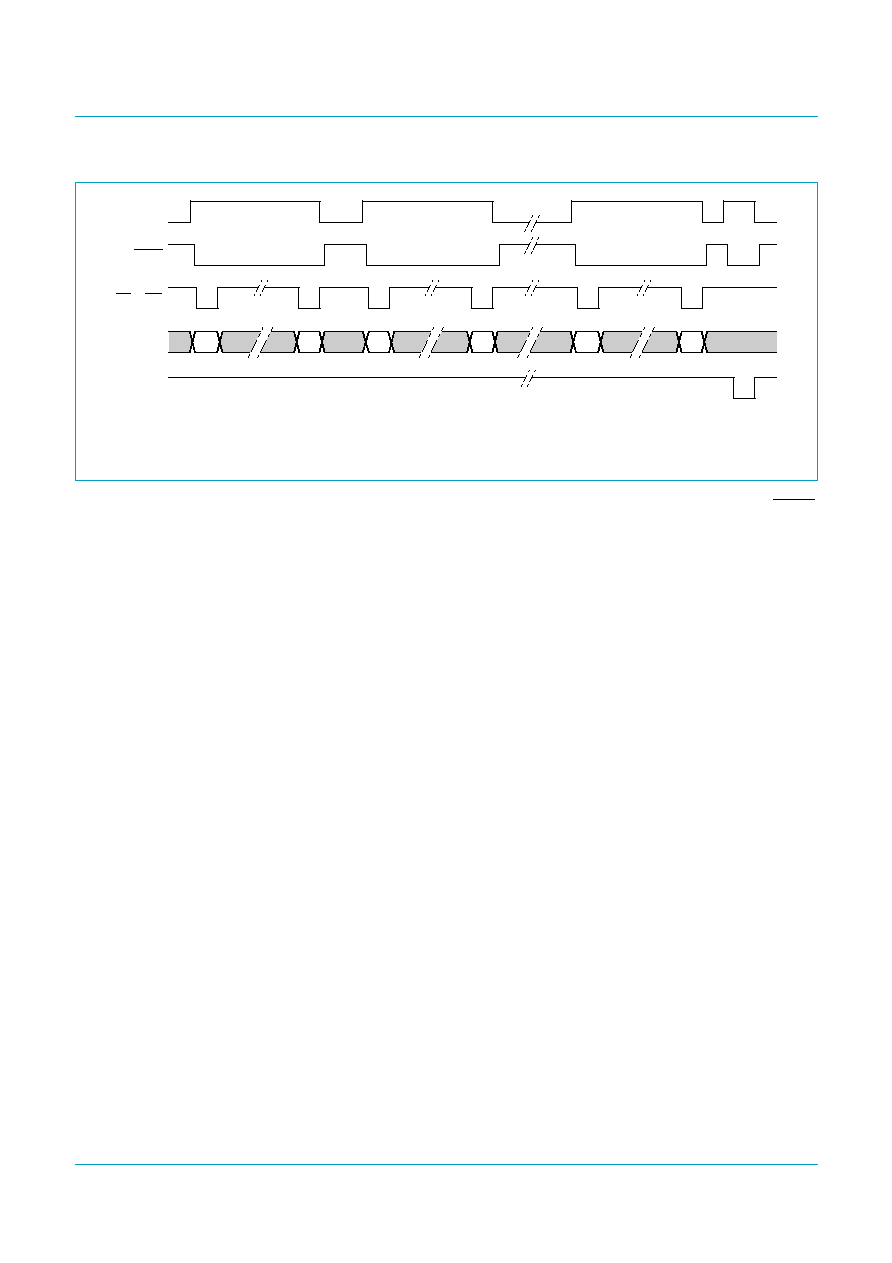
N = 1/2 byte count of transfer data.
Fig 17. DMA transfer in single-cycle mode.
004aaa103
DREQ
DACK
D[15:0]
EOT
data #1
data #2
data #N
RD or WR
Philips Semiconductors
ISP1161A1
USB single-chip host and device controller
Product data
Rev. 03 -- 23 December 2004
18 of 136
9397 750 13961
© Koninklijke Philips Electronics N.V. 2004. All rights reserved.
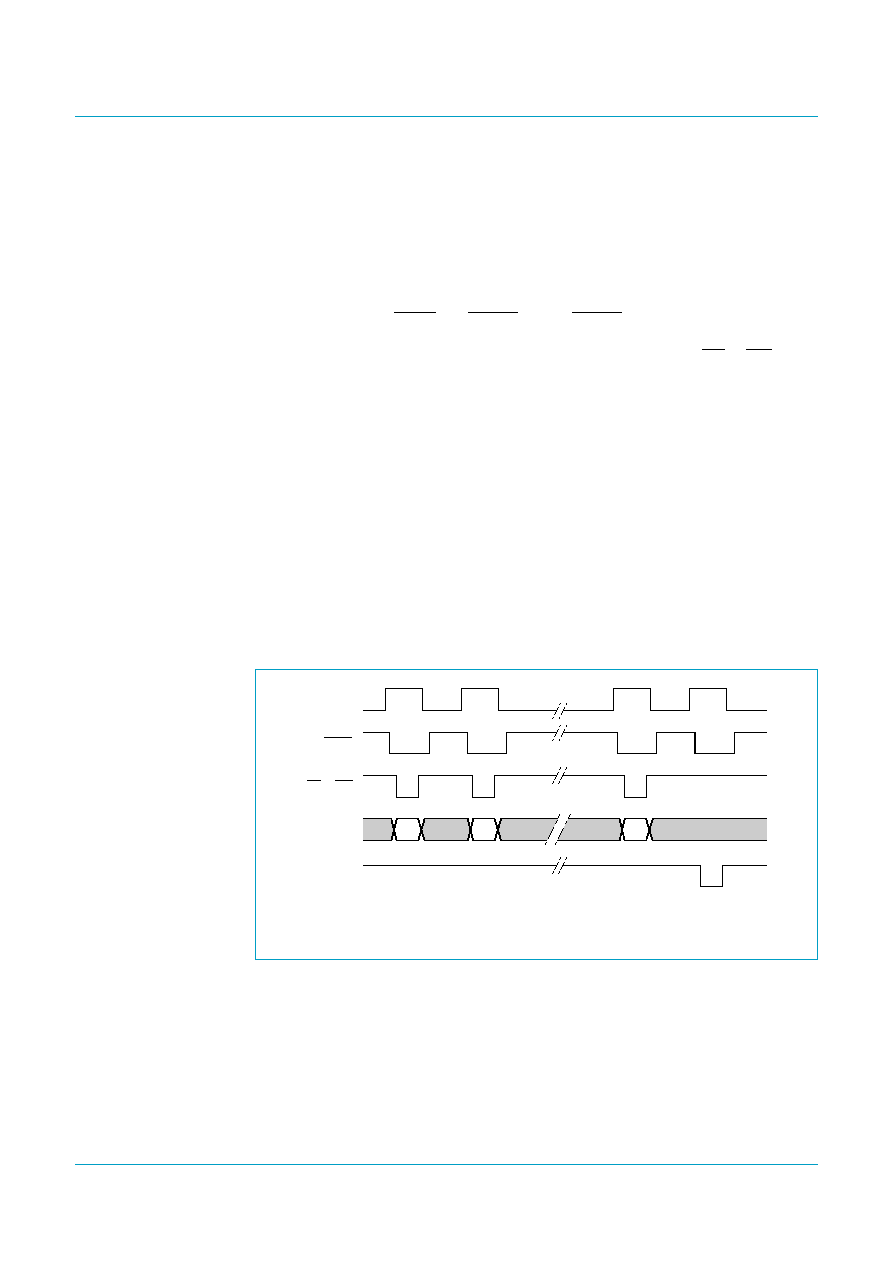
In both figures, the hardware is configured such that DREQ is active HIGH and DACK
is active LOW.
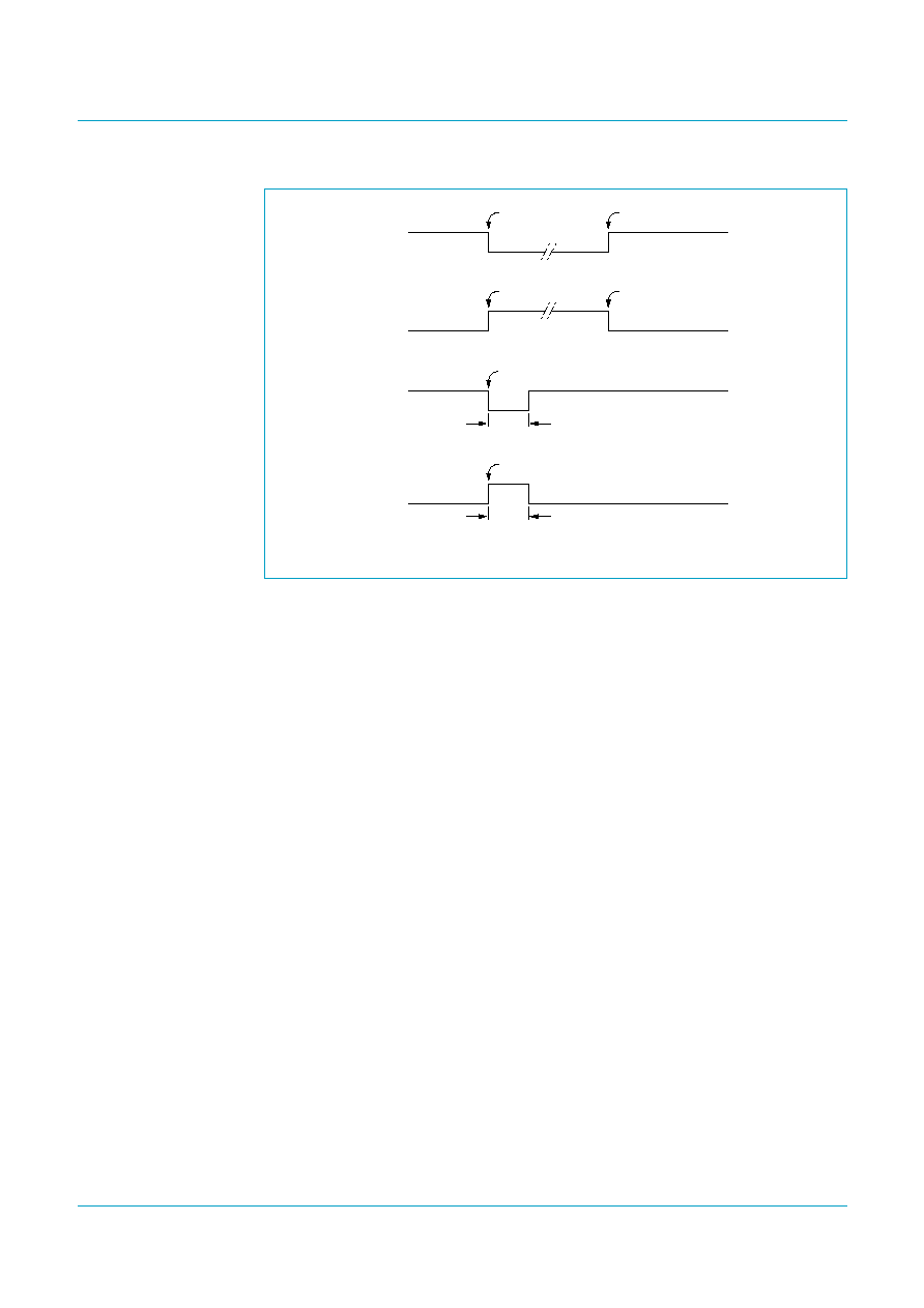
8.6 Interrupts
The ISP1161A1 has separate interrupt request pins for the USB HC (INT1) and the
USB DC (INT2).
8.6.1
Pin configuration
The interrupt output signals have four configuration modes:
Mode 0
Level trigger, active LOW (default at power-up)
Mode 1
Level trigger, active HIGH
Mode 2
Edge trigger, active LOW
Mode 3
Edge trigger, active HIGH.
Figure 19
shows these four interrupt configuration modes. They are programmable
via the HcHardwareConfiguration register (see
Section 10.4.1
), which is also used to
disable or enable the signals.
N = 1/2 byte count of transfer data, K = number of cycles/burst.
Fig 18. DMA transfer in burst mode.
004aaa104
data #1
data #K
data #2K
data #N
data #(K
+
1)
data #(N
-
K
+
1)
DREQ
DACK
D[15:0]
EOT
RD or WR
Philips Semiconductors
ISP1161A1
USB single-chip host and device controller
Product data
Rev. 03 -- 23 December 2004
19 of 136
9397 750 13961
© Koninklijke Philips Electronics N.V. 2004. All rights reserved.
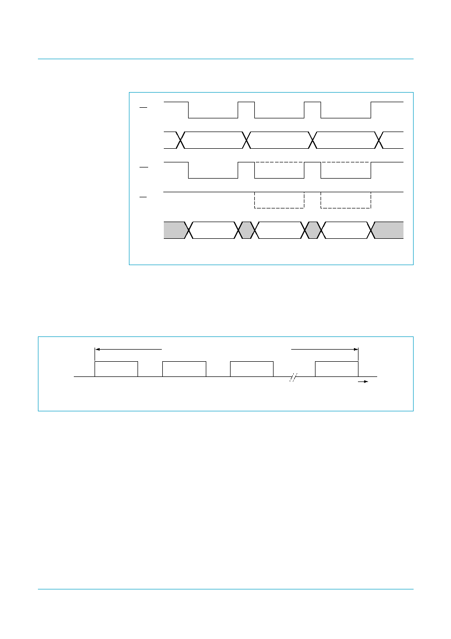
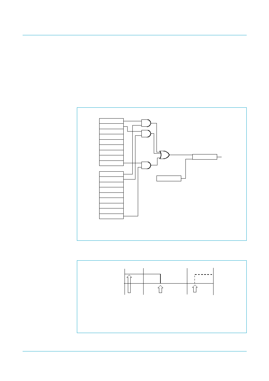
8.6.2
HC's interrupt output pin (INT1)
To program the four configuration modes of the HC's interrupt output signal (INT1),
set bits InterruptPinTrigger and InterruptOutputPolarity of the
HcHardwareConfiguration register (20H to read, A0H to write). Bit InterruptPinEnable
is used as the master enable setting for pin INT1.
INT1 has many associated interrupt events, as shown as in
Figure 20
.
The interrupt events of the Hc
µ
PInterrupt register (24H to read, A4H to write)
changes the status of pin INT1 when the corresponding bits of the
Hc
µ
PInterruptEnable register (25H to read, A5H to write) and pin INT1's global
enable bit (InterruptPinEnable of the HcHardwareConfiguration register) are all set to
enable status.
However, events that come from the HcInterruptStatus register (03H to read, 83H to
write) affect only bit OPR_Reg of the Hc
µ
PInterrupt register. They cannot directly
change the status of pin INT1.
Fig 19. Interrupt pin operating modes.
MGT944
INT active
INT active
clear or disable INT
Mode 1 level triggered, active HIGH
INT
INT
166 ns
Mode 2 edge triggered, active LOW
INT active
INT
166 ns
Mode 3 edge triggered, active HIGH
INT active
clear or disable INT
Mode 0 level triggered, active LOW
INT
Philips Semiconductors
ISP1161A1
USB single-chip host and device controller
Product data
Rev. 03 -- 23 December 2004
20 of 136
9397 750 13961
© Koninklijke Philips Electronics N.V. 2004. All rights reserved.
There are two groups of interrupts represented by group 1 and group 2 in
Figure 20
.
A pair of registers control each group.
Group 2 contains six possible interrupt events (recorded in the HcInterruptStatus
register). On occurrence of any of these events, the corresponding bit would be set to
logic 1; and if the corresponding bit in the HcInterruptEnable register is also logic 1,
the 6-input OR gate would output a logic 1. This output is AND-ed with the value of
MIE (bit 31 of HcInterruptEnable). Logic 1 at the AND gate will cause bit OPR in the
Hc
µ
PInterrupt register to be set to logic 1.
Group 1 contains six possible interrupt events, one of which is the output of group 2
interrupt sources. The Hc
µ
PInterrupt and Hc
µ
PInterruptEnable registers work in the
same way as the HcInterruptStatus and HcInterruptEnable registers in the interrupt
group 2. The output from the 6-input OR gate is connected to a latch, which is
controlled by InterruptPinEnable (bit 0 of the HcHardwareConfiguration register).
In the event in which the software wishes to temporarily disable the interrupt output of
the ISP1161A1 Host Controller, the following procedure should be followed:
1. Make sure that bit InterruptPinEnable in the HcHardwareConfiguration register is
set to logic 1.
2. Clear all bits in the Hc
µ
PInterrupt register.
3. Set bit InterruptPinEnable to logic 0.
Fig 20. HC interrupt logic.
MGT945
SOFITLInt
ATLInt
AllEOTInterrupt
OPR_Reg
HCSuspended
HcµPInterrupt
register
HcInterruptEnable
register
HcInterruptStatus
register
ClkReady
RHSC
FNO
UE
RD
SF
SO
RHSC
FNO
UE
RD
SF
SO
MIE
OR
SOFITLInt
ATLInt
AllEOTInterrupt
OPR_Reg
HCSuspended
HcµPInterruptEnable
register
ClkReady
OR
LATCH
INT1
group 2
InterruptPinEnable
HcHardwareConfiguration
register
group 1
LE

Philips Semiconductors
ISP1161A1
USB single-chip host and device controller
Product data
Rev. 03 -- 23 December 2004
21 of 136
9397 750 13961
© Koninklijke Philips Electronics N.V. 2004. All rights reserved.
To re-enable the interrupt generation:
1. Set all bits in the Hc
µ
PInterrupt register.
2. Set bit InterruptPinEnable to logic 1.
Remark: Bit InterruptPinEnable in the HcHardwareConfiguration register latches the
interrupt output. When this bit is set to logic 0, the interrupt output will remain
unchanged, regardless of any operations on the interrupt control registers.
If INT1 is asserted, and the HCD wishes to temporarily mask off the INT signal
without clearing the Hc
µ
PInterrupt register, the following procedure should be
followed:
1. Make sure that bit InterruptPinEnable is set to logic 1.
2. Clear all bits in the Hc
µ
PInterruptEnable register.
3. Set bit InterruptPinEnable to logic 0.
To re-enable the interrupt generation:
1. Set all bits in the Hc
µ
PInterruptEnable register according to the HCD
requirements.
2. Set bit InterruptPinEnable to logic 1.
8.6.3
DC interrupt output pin (INT2)
The four configuration modes of DC's interrupt output pin INT2 can also be
programmed by setting bits INTPOL and INTLVL of the DcHardwareConfiguration
register (BBH to read, BAH to write). Bit INTENA of the DcMode register (B9H to
read, B8H to write) is used to enable pin INT2.
Figure 21
shows the relationship
between the interrupt events and pin INT2.
Each of the indicated USB events is logged in a status bit of the DcInterrupt register.
Corresponding bits in the DcInterruptEnable register determine whether or not an
event will generate an interrupt.
Interrupts can be masked globally by means of bit INTENA of the DcMode register
(see
Table 81
).
The active level and signalling mode of the INT output is controlled by bits INTPOL
and INTLVL of the DcHardwareConfiguration register (see
Table 83
). Default settings
after reset are active LOW and level mode. When pulse mode is selected, a pulse of
166 ns is generated when the OR-ed combination of all interrupt bits changes from
logic 0 to logic 1.
Bits RESET, RESUME, SP_EOT, EOT and SOF are cleared upon reading the
DcInterrupt register. The endpoint bits (EP0OUT to EP14) are cleared by reading the
associated DcEndpointStatus register.
Bit BUSTATUS follows the USB bus status exactly, allowing the firmware to get the
current bus status when reading the DcInterrupt register.
SETUP and OUT token interrupts are generated after the DC has acknowledged the
associated data packet. In bulk transfer mode, the DC will issue interrupts for every
ACK received for an OUT token or transmitted for an IN token.
Philips Semiconductors
ISP1161A1
USB single-chip host and device controller
Product data
Rev. 03 -- 23 December 2004
22 of 136
9397 750 13961
© Koninklijke Philips Electronics N.V. 2004. All rights reserved.
In isochronous mode, an interrupt is issued upon each packet transaction. The
firmware must take care of timing synchronization with the host. This can be done via
the Pseudo Start-Of-Frame (PSOF) interrupt, enabled via bit IEPSOF in the
DcInterruptEnable register. If a Start-Of-Frame is lost, PSOF interrupts are generated
every 1 ms. This allows the firmware to keep data transfer synchronized with the host.
After 3 missed SOF events, the DC will enter `suspend' state.
An alternative way of handling isochronous data transfer is to enable both the SOF
and the PSOF interrupts and disable the interrupt for each isochronous endpoint.
Interrupt control:
Bit INTENA in the DcMode register is a global enable/disable bit.
The behavior of this bit is given in
Figure 22
.
Fig 21. DC interrupt logic.
Pin INT2: HIGH = de-assert; LOW = assert (individual interrupts are enabled).
Fig 22. Behavior of bit INTENA.
MGT946
RESET
SUSPND
RESUME
SOF
EP14
. . .
EP0IN
.
.
.
.
.
.
.
.
.
.
.
.
EP0OUT
EOT
IERST
DcInterrupt register
DcInterruptEnable register
IESUSP
IERESM
IESOF
IEP14
. . .
IEP0IN
IEP0OUT
IEEOT
DcMode register
INTENA
INT2
LATCH
LE
INT2 pin
004aaa198
INTENA = 0
SOF asserted
INTENA = 1
SOF asserted
INTENA = 0
(during this time,
an interrupt event
occurs. For example,
SOF asserted.)
A
B
C

Philips Semiconductors
ISP1161A1
USB single-chip host and device controller
Product data
Rev. 03 -- 23 December 2004
23 of 136
9397 750 13961
© Koninklijke Philips Electronics N.V. 2004. All rights reserved.
Event A (see
Figure 22
): When an interrupt event occurs (for example, SOF interrupt)
with bit INTENA set to logic 0, an interrupt will not be generated at pin INT2.
However, it will be registered in the corresponding DcInterrupt register bit.
Event B (see
Figure 22
): When bit INTENA is set to logic 1, pin INT2 is asserted
because bit SOF in the DcInterrupt register is already asserted.
Event C (see
Figure 22
): If the firmware sets bit INTENA to logic 0, pin INT2 will still
be asserted. The bold dashed line shows the desired behavior of pin INT2.
De-assertion of pin INT2 can be achieved in the following manner. Bits[23:8] of the
DcInterrupt register are endpoint interrupts. These interrupts are cleared on reading
their respective DcEndpointStatus register. Bits[7:0] of the DcInterrupt register are
bus status and EOT interrupts that are cleared on reading the DcInterrupt register.
Make sure that bit INTENA is set to logic 1 when you perform the clear interrupt
commands.
For more information on interrupt control, see
Section 13.1.3
,
Section 13.1.5
and
Section 13.3.6
.
Philips Semiconductors
ISP1161A1
USB single-chip host and device controller
Product data
Rev. 03 -- 23 December 2004
24 of 136
9397 750 13961
© Koninklijke Philips Electronics N.V. 2004. All rights reserved.
9.
USB host controller (HC)
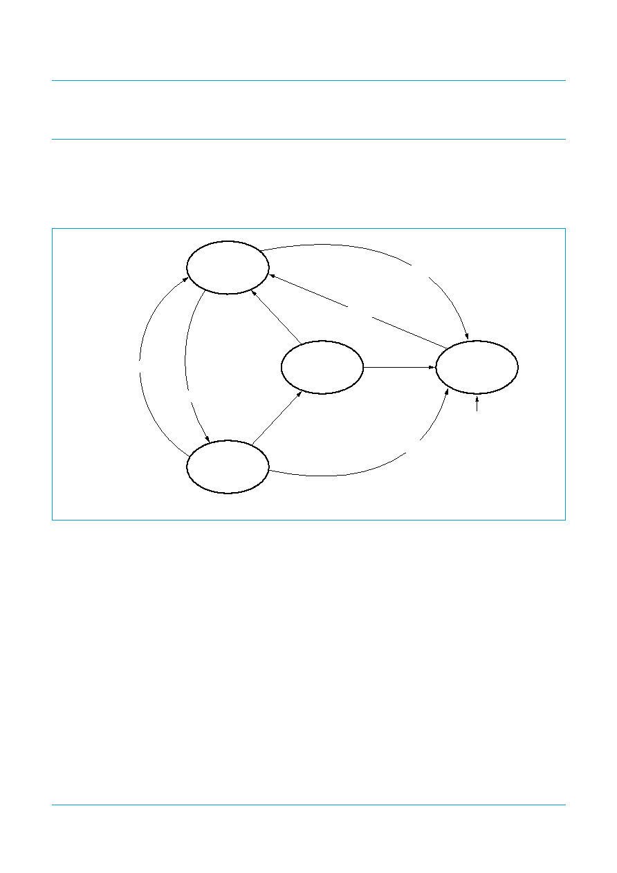
9.1 HC's four USB states
The ISP1161A1 USB HC has four USB states
-
USBOperational, USBReset,
USBSuspend, and USBResume
-
that define the HC's USB signaling and bus states
responsibilities.
The USB states are reflected in the HostControllerFunctionalState field of the
HcControl register (01H to read, 81H to write), which is located at bits 7 and 6 of the
register.
The Host Controller Driver (HCD) can perform only the USB state transitions shown
in
Figure 23
.
Remark: The Software Reset in
Figure 23
is not caused by the HcSoftwareReset
command. It is caused by the HostControllerReset field of the HcCommandStatus
register (02H to read, 82H to write).
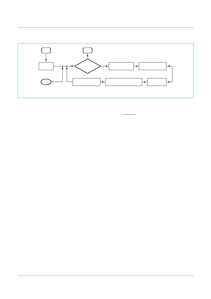
9.2 Generating USB traffic
USB traffic can be generated only when the ISP1161A1 USB HC is in the
USBOperational state. Therefore, the HCD must set the
HostControllerFunctionalState field of the HcControl register before generating USB
traffic.
A simplistic flow diagram showing when and how to generate USB traffic is shown in
Figure 24
. For more detail, refer to the
USB Specification Revision 2.0 about the
protocol and ISP1161A1 USB HC register usage.
Fig 23. ISP1161A1 HC USB states.
MGT947
USBOperational
USBSuspend
USBResume
USBResume write
or
remote wake-up
USBReset
USBOperational write
USBOperational write
USBSuspend write
USBReset write
USBReset write
USBReset write
hardware or software
reset
Philips Semiconductors
ISP1161A1
USB single-chip host and device controller
Product data
Rev. 03 -- 23 December 2004
25 of 136
9397 750 13961
© Koninklijke Philips Electronics N.V. 2004. All rights reserved.
Description of
Figure 24
:
1. Reset
This includes hardware reset by pin RESET and software reset by the
HcSoftwareReset command (A9H). The reset function will clear all the HC's
internal control registers to their reset status. After reset, the HCD must initialize
the ISP1161A1 USB HC by setting some registers.
2. Initialize HC
It includes:
a. Setting the physical size for the HC's internal FIFO buffer RAM by setting the
HcITLBufferLength register (2AH to read, AAH to write) and the
HcATLBufferLength register (2BH to read, ABH to write)
b. Setting the HcHardwareConfiguration register according to requirements
c. Clearing interrupt events, if required
d. Enabling interrupt events, if required
e. Setting the HcFmInterval register (0DH to read, 8DH to write)
f. Setting the HC's Root Hub registers
g. Setting the HcControl register to move the HC into USBOperational state
See also
Section 9.5
.
3. Entry
The normal entry point. The microprocessor returns to this point when there
are HC requests.
4. Need USB traffic
USB devices need the HC to generate USB traffic when they have USB traffic
requests such as:
a. Connecting to or disconnecting from the downstream ports
b. Issuing the Resume signal to the HC
To generate USB traffic, the HCD must enter the USB transaction loop.
5. Prepare PTD data in microprocessor's system RAM
The communication between the HCD and the ISP1161A1 HC is in the form of
Philips Transfer Descriptor (PTD) data. The PTD data provides USB traffic
information about the commands, status, and USB data packets.
Fig 24. ISP1161A1 HC USB transaction loop.
MGT948
Need
USB traffic?
Prepare PTD data in
µ
P system RAM
Initialize
HC
Transfer PTD data into
HC FIFO buffer RAM
HC performs USB transactions
via USB bus I/F
HC informs HCD of
USB traffic results
HC interprets
PTD data
Exit
Entry
HC state =
USBOperational
no
yes
Reset
Philips Semiconductors
ISP1161A1
USB single-chip host and device controller
Product data
Rev. 03 -- 23 December 2004
26 of 136
9397 750 13961
© Koninklijke Philips Electronics N.V. 2004. All rights reserved.
The physical storage media of PTD data for the HCD is the microprocessor's
system RAM. For the ISP1161A1 HC, the storage media is the internal FIFO
buffer RAM.
The HCD prepares PTD data in the microprocessor system RAM for transfer to
the ISP1161A1 HC internal FIFO buffer RAM.
6. Transfer PTD data into HC's FIFO buffer RAM
When PTD data is ready in the microprocessor's system RAM, the HCD must
transfer the PTD data from the microprocessor's system RAM into the
ISP1161A1 internal FIFO buffer RAM.
7. HC interprets PTD data
The HC determines what USB transactions are required based on the PTD data
that has been transferred into the internal FIFO buffer RAM.
8. HC performs USB transactions via USB bus interface
The HC performs the USB transactions with the specified USB device endpoint
through the USB bus interface.
9. HC informs HCD of the USB traffic results
The USB transaction status and the feedback from the specified USB device
endpoint will be put back into the ISP1161A1 HC internal FIFO buffer RAM in
PTD data format. The HCD can read back the PTD data from the internal FIFO
buffer RAM.
9.3 PTD data structure
The Philips Transfer Descriptor (PTD) data structure provides communication
between the HCD and the ISP1161A1 USB HC. The PTD data contains information
required by the USB traffic. PTD data consists of a PTD followed by its payload data,
as shown in
Figure 25
.
The PTD data structure is used by the HC to define a buffer of data that will be moved
to or from an endpoint in the USB device. This data buffer is set up for the current
frame (1 ms frame) by the HCD. The payload data for every transfer in the frame must
have a PTD as a header to describe the characteristics of the transfer. PTD data is
DWORD (double-word or 4-byte) aligned.
Fig 25. PTD data in FIFO buffer RAM.
MGT949
PTD
FIFO buffer RAM
payload data
PTD data #1
PTD
payload data
payload data
PTD
PTD data #2
PTD data #N
top
bottom

Philips Semiconductors
ISP1161A1
USB single-chip host and device controller
Product data
Rev. 03 -- 23 December 2004
27 of 136
9397 750 13961
© Koninklijke Philips Electronics N.V. 2004. All rights reserved.
9.3.1
PTD data header definition
The PTD forms the header of the PTD data. It tells the HC the transfer type, where
the payload data should go, and the actual size of the payload data. A PTD is an
8 byte data structure that is very important for HCD programming.
Table 4:
Philips Transfer Descriptor (PTD): bit allocation
Bit
7
6
5
4
3
2
1
0
Byte 0
ActualBytes[7:0]
Byte 1
CompletionCode[3:0]
Active
Toggle
ActualBytes[9:8]
Byte 2
MaxPacketSize[7:0]
Byte 3
EndpointNumber[3:0]
Last
Speed
MaxPacketSize[9:8]
Byte 4
TotalBytes[7:0]
Byte 5
reserved
B5_5
reserved
DirectionPID[1:0]
TotalBytes[9:8]
Byte 6
Format
FunctionAddress[6:0]
Byte 7
reserved

Philips Semiconductors
ISP1161A1
USB single-chip host and device controller
Product data
Rev. 03 -- 23 December 2004
28 of 136
9397 750 13961
© Koninklijke Philips Electronics N.V. 2004. All rights reserved.
Table 5:
Philips Transfer Descriptor (PTD): bit description
Symbol
Access Description
ActualBytes[9:0]
R/W
Contains the number of bytes that were transferred for this PTD
CompletionCode[3:0]
R/W
0000
NoError
General TD or isochronous data packet processing
completed with no detected errors.
0001
CRC
Last data packet from endpoint contained a CRC error.
0010
BitStuffing
Last data packet from endpoint contained a bit stuffing
violation.
0011
DataToggleMismatch
Last packet from endpoint had data toggle PID that did
not match the expected value.
0100
Stall
TD was moved to the Done queue because the
endpoint returned a STALL PID.
0101
DeviceNotResponding
Device did not respond to token (IN) or did not provide a
handshake (OUT).
0110
PIDCheckFailure
Check bits on PID from endpoint failed on data PID (IN)
or handshake (OUT)
0111
UnexpectedPID
Received PID was not valid when encountered or PID
value is not defined.
1000
DataOverrun
The amount of data returned by the endpoint exceeded
either the size of the maximum data packet allowed
from the endpoint (found in the MaxPacketSize field of
ED) or the remaining buffer size.
1001
DataUnderrun
The endpoint returned is less than MaxPacketSize and
that amount was not sufficient to fill the specified buffer.
1010
reserved
-
1011
reserved
-
1100
BufferOverrun
During an IN, the HC received data from an endpoint
faster than it could be written to system memory.
1101
BufferUnderrun
During an OUT, the HC could not retrieve data from the
system memory fast enough to keep up with the USB
data rate.
Active
R/W
Set to logic 1 by firmware to enable the execution of transactions by the HC. When the
transaction associated with this descriptor is completed, the HC sets this bit to logic 0,
indicating that a transaction for this element will not be executed when it is next
encountered in the schedule.
Toggle
R/W
Used to generate or compare the data PID value (DATA0 or DATA1). It is updated after
each successful transmission or reception of a data packet.
MaxPacketSize[9:0]
R
The maximum number of bytes that can be sent to or received from the endpoint in a
single data packet.
EndpointNumber[3:0]
R
USB address of the endpoint within the function.
Last
R
Last PTD of a list (ITL or ATL). Logic 1 indicates that the PTD is the last PTD.
Speed
R
Speed of the endpoint:
0 -- full speed
1 -- low speed
TotalBytes[9:0]
R
Specifies the total number of bytes to be transferred with this data structure. For Bulk and
Control only, this can be greater than MaxPacketSize.

Philips Semiconductors
ISP1161A1
USB single-chip host and device controller
Product data
Rev. 03 -- 23 December 2004
29 of 136
9397 750 13961
© Koninklijke Philips Electronics N.V. 2004. All rights reserved.
9.4 HC internal FIFO buffer RAM structure
9.4.1
Partitions
According to the
Universal Serial Bus Specification Rev. 2.0, there are four types of
USB data transfers: Control, Bulk, Interrupt and Isochronous.
The HC's internal FIFO buffer RAM has a physical size of 4 kbytes. This internal FIFO
buffer RAM is used for transferring data between the microprocessor and USB
peripheral devices. This on-chip buffer RAM can be partitioned into two areas:
Acknowledged Transfer List (ATL) buffer and Isochronous (ISO) Transfer List (ITL)
buffer. The ITL buffer is a Ping-Pong structured FIFO buffer RAM that is used to keep
the payload data and their PTD header for Isochronous transfers. The ATL buffer is a
non Ping-Pong structured FIFO buffer RAM that is used for the other three types of
transfers.
The ITL buffer can be further partitioned into ITL0 and ITL1 for the Ping-Pong
structure. The ITL0 buffer and ITL1 buffer always have the same size. The
microprocessor can put ISO data into either the ITL0 buffer or the ITL1 buffer. When
the microprocessor accesses an ITL buffer, the HC can take over the other ITL buffer
at the same time. This architecture improves the ISO transfer performance.
The HCD can assign the logical size for the ATL buffer and ITL buffers at any time, but
normally at initialization after power-on reset. This is done by setting the
HcATLBufferLength register (2BH to read, ABH to write) and HcITLBufferLength
register (2AH to read, AAH to write). The total buffer length cannot exceed the
maximum RAM size of 4 kbytes (ATL buffer + ITL buffer).
Figure 26
shows the
partitions of the internal FIFO buffer RAM. When assigning buffer RAM sizes, follow
this formula:
ATL buffer length + 2
×
(ITL buffer size)
1000H (that is, 4 kbytes)
where: ITL buffer size = ITL0 buffer length = ITL1 buffer length
The following assignments are examples of legal uses of the internal FIFO buffer
RAM:
·
ATL buffer length = 800H, ITL buffer length = 400H.
This is the maximum use of the internal FIFO buffer RAM.
DirectionPID[1:0]
R
00 -- SETUP
01 -- OUT
10 -- IN
11 -- reserved
B5_5
R/W
This bit is logic 0 at power-on reset. When this feature is not used, software used for the
ISP1161A1 is the same for the ISP1160 and the ISP1161. When this bit is set to logic 1
in this PTD for interrupt endpoint transfer, only one PTD USB transaction will be sent out
in 1 ms.
Format
R
The format of this data structure. If this is a Control, Bulk or Interrupt endpoint, then
Format = 0. If this is an Isochronous endpoint, then Format = 1.
FunctionAddress[6:0]
R
This is the USB address of the function containing the endpoint that this PTD refers to.
Table 5:
Philips Transfer Descriptor (PTD): bit description
...continued
Symbol
Access Description
Philips Semiconductors
ISP1161A1
USB single-chip host and device controller
Product data
Rev. 03 -- 23 December 2004
30 of 136
9397 750 13961
© Koninklijke Philips Electronics N.V. 2004. All rights reserved.
·
ATL buffer length = 400H, ITL buffer length = 200H.
This is insufficient use of the internal FIFO buffer RAM.
·
ATL buffer length = 1000H, ITL buffer length = 0H.
This will use the internal FIFO buffer RAM for only ATL transfers.
The actual requirement for the buffer RAM need not reach the maximum size. You
can make your selection based on your application.
The following are some calculations of the ISO_A or ISO_B space for a frame of data:
·
Maximum number of useful data sent during one USB frame is 1280 bytes (20
ISO packets of 64 bytes). The total RAM size needed is:
20
×
8 + 1280 = 1440 bytes.
·
Maximum number of packets for different endpoints sent during one USB frame is
150 (150 ISO packets of 1 byte). The total RAM size needed is:
150
×
8 + 150
×
1 = 1350 bytes.
·
The Ping buffer RAM (ITL0) and the Pong buffer RAM (ITL1) have a maximum size
of 2 kbytes each. All data needed for one frame can be stored in the Ping or the
Pong buffer RAM.
When the embedded system wants to initiate a transfer to the USB bus, the data
needed for one frame is transferred to the ATL buffer or ITL buffer. The
microprocessor detects the buffer status through the interrupt routines. When the
HcBufferStatus register (2CH to read only) indicates that the buffer is empty, then the
microprocessor writes data into the buffer. When the HcBufferStatus register
indicates that the buffer is full, the data is ready on the buffer, and the microprocessor
needs to read data from the buffer.
During every 1 ms, there might be many events to generate interrupt requests to the
microprocessor for data transfer or status retrieval. However, each of the interrupt
types defined in this specification can be enabled or disabled by setting the
Hc
µ
PInterruptEnable register bits accordingly.
Fig 26. HC internal FIFO buffer RAM partitions.
MGT950
not used
ATL buffer
ITL0
top
bottom
ITL1
ISO_A
FIFO buffer RAM
ISO_B
control/bulk/interrupt
data
programmable
sizes
4 kbytes
ITL buffer
ATL
Philips Semiconductors
ISP1161A1
USB single-chip host and device controller
Product data
Rev. 03 -- 23 December 2004
31 of 136
9397 750 13961
© Koninklijke Philips Electronics N.V. 2004. All rights reserved.
The data transfer can be done via the PIO mode or the DMA mode. The data transfer
rate can go up to 15 Mbyte/s. In the DMA operation, the single-cycle or multi-cycle
burst modes are supported. Multi-cycle burst modes of 1, 4, or 8 cycles per burst is
supported for the ISP1161A1.
9.4.2
Data organization
PTD data is used for every data transfer between a microprocessor and the USB bus,
and the PTD data resides in the buffer RAM. For an OUT or SETUP transfer, the
payload data is placed just after the PTD, after which the next PTD is placed. For an
IN transfer, RAM space is reserved for receiving a number of bytes that is equal to the
total bytes of the transfer. After this, the next PTD and its payload data are placed
(see
Figure 27
).
Remark:
The PTD is defined for both ATL and ITL type data transfers. For ITL, the PTD data is
put into ITL buffer RAM, and the ISP1161A1 takes care of the Ping-Pong action for
the ITL buffer RAM access.
The PTD data (PTD header and its payload data) is a structure of DWORD (double-
word or 4-byte) alignment. This means that the memory address is organized in
blocks of 4 bytes. Therefore, the first byte of every PTD and the first byte of every
payload data are located at an address which is a multiple of 4.
Figure 28
illustrates
an example in which the first payload data is 14 bytes long, meaning that the last byte
of the payload data is at the location 15H. The next addresses (16H and 17H) are not
multiples of 4. Therefore, the first byte of the next PTD will be located at the next
multiple-of-four address, 18H.
Fig 27. Buffer RAM data organization.
MGT952
PTD of OUT transfer
RAM buffer
payload data of OUT transfer
PTD of IN transfer
empty space for IN total data
PTD of OUT transfer
payload data of OUT transfer
top
bottom
000H
7FFH

Philips Semiconductors
ISP1161A1
USB single-chip host and device controller
Product data
Rev. 03 -- 23 December 2004
32 of 136
9397 750 13961
© Koninklijke Philips Electronics N.V. 2004. All rights reserved.
9.4.3
Operation and C program example
Figure 29
shows the block diagram for internal FIFO buffer RAM operations in the
PIO mode. The ISP1161A1 provides one register as the access port for each buffer
RAM. For the ITL buffer RAM, the access port is the ITLBufferPort register (40H to
read, C0H to write). For the ATL buffer RAM, the access port is the ATLBufferPort
register (41H to read, C1H to write). The buffer RAM is an array of bytes (8 bits) while
the access port is a 16-bit register. Therefore, each read/write operation on the port
accesses two consecutive memory locations, incrementing the pointer of the internal
buffer RAM by two.
The lower byte of the access port register corresponds to the data byte at the even
location of the buffer RAM, and the upper byte corresponds to the next data byte at
the odd location of the buffer RAM. Regardless of the number of data bytes to be
transferred, the command code must be issued merely once, and it will be followed by
a number of accesses of the data port (see
Section 8.4
).
When the pointer of the buffer RAM reaches the value of the HcTransferCounter
register, an internal EOT signal will be generated to set bit 2, AllEOTInterrupt, of the
Hc
µ
PInterrupt register and update the HcBufferStatus register, to indicate that the
whole data transfer has been completed.
For ITL buffer RAM, every Start Of Frame (SOF) signal (1 ms) will cause toggling
between ITL0 and ITL1, but this depends on the buffer status. If both ITL0BufferFull
and ITL1BufferFull of the HcBufferStatus register are already logic 1, meaning that
both ITL0 and ITL1 buffer RAMs are full, the toggling will not happen. In this case, the
microprocessor will always have access to ITL1.
Fig 28. PTD data with DWORD alignment in buffer RAM.
MGT953
payload data
(14 bytes)
PTD
(8 bytes)
PTD
(8 bytes)
00H
top
08H
15H
18H
20H
payload data
RAM buffer
Philips Semiconductors
ISP1161A1
USB single-chip host and device controller
Product data
Rev. 03 -- 23 December 2004
33 of 136
9397 750 13961
© Koninklijke Philips Electronics N.V. 2004. All rights reserved.
Following is an example of a C program that shows how to write data into the ATL
buffer RAM. The total number of data bytes to be transferred is 80 (decimal) that will
be set into the HcTransferCounter register as 50H. The data consists of four types of
PTD data:
1. The first PTD header (IN) is 8 bytes, followed by 16 bytes of space reserved for
its payload data;
2. The second PTD header (IN) is also 8 bytes, followed by 8 bytes of space
reserved for its payload data;
3. The third PTD header (OUT) is 8 bytes, followed by 16 bytes of payload data with
values beginning from 0H to FH incrementing by 1;
4. The fourth PTD header (OUT) is also 8 bytes, followed by 8 bytes of payload data
with values beginning from 0H to EH incrementing by 2.
In all PTDs, we have assigned device address as 5 and endpoint as 1. ActualBytes is
always zero (0). TotalBytes equals the number of payload data bytes transferred,
however, note that for bulk and control transfers, TotalBytes can be greater than
MaxPacketSize.
Table 6
shows the results after running this program.
Fig 29. PIO access to internal FIFO buffer RAM.
MGT951
Commands
Pointer
automatically
increments by 2
TransferCounter
BufferStatus
BufferStatus
internal EOT
ITLBufferPort
ATLBufferPort
ATL buffer RAM
(8-bit width)
Control registers
Command register
data port
T
EOT
1
2
=
0
toggle
command port
µ
PInterrupt
22H/A2H
2CH
40H/C0H
41H/C1H
24H/A4H
000H
7FFH
001H
ITL1 buffer RAM
(8-bit width)
000H
3FFH
001H
ITL0 buffer RAM
(8-bit width)
000H
3FFH
001H
A0
Host bus I/F
1
0
(16-bit width)
SOF

Philips Semiconductors
ISP1161A1
USB single-chip host and device controller
Product data
Rev. 03 -- 23 December 2004
34 of 136
9397 750 13961
© Koninklijke Philips Electronics N.V. 2004. All rights reserved.
If communication with a peripheral USB device is desired, however, the device should
be connected to the downstream port and pass enumeration.
// The example program for writing ATL buffer RAM
#include <conio.h>
#include <stdio.h>
#include <dos.h>
// Define register commands
#define wHcTransferCounter 0x22
#define wHcuPInterrupt 0x24
#define wHcATLBufferLength 0x2b
#define wHcBufferStatus 0x2c
// Define I/O Port Address for HC
#define HcDataPort 0x290
#define HcCmdPort 0x292
// Declare external functions to be used
unsigned int HcRegRead(unsigned int wIndex);
void HcRegWrite(unsigned int wIndex,unsigned int wValue);
void main(void)
{
unsigned int i;
unsigned int wCount,wData;
// Prepare PTD data to be written into HC ATL buffer RAM:
unsigned int PTDData[0x28]=
{
0x0800,0x1010,0x0810,0x0005, // PTD header for IN token #1
// Reserved space for payload data of IN token #1
0x0000,0x0000,0x0000,0x0000, 0x0000,0x0000,0x0000,0x0000,
0x0800,0x1008,0x0808,0x0005, // PTD header for IN token #2
// Reserved space for payload data of IN token #2
0x0000,0x0000,0x0000,0x0000,
0x0800,0x1010,0x0410,0x0005, // PTD header for OUT token #1
0x0100,0x0302,0x0504,0x0706, // Payload data for OUT token #1
0x0908,0x0b0a,0x0d0c,0x0f0e,
0x0800,0x1808,0x0408,0x0005, // PTD header for OUT token #2
0x0200,0x0604,0x0a08,0x0e0c // Payload data for OUT token #2
};
HcRegWrite(wHcuPInterrupt,0x04); // Clear EOT interrupt bit
// HcRegWrite(wHcITLBufferLength,0x0);
HcRegWrite(wHcATLBufferLength,0x1000); // RAM full use for ATL
// Set the number of bytes to be transferred
HcRegWrite(wHcTransferCounter,0x50);
wCount = 0x28; // Get word count outport
(HcCmdPort,0x00c1); // Command for ATL buffer write

Philips Semiconductors
ISP1161A1
USB single-chip host and device controller
Product data
Rev. 03 -- 23 December 2004
35 of 136
9397 750 13961
© Koninklijke Philips Electronics N.V. 2004. All rights reserved.
// Write 80 (0x50) bytes of data into ATL buffer RAM
for (i=0;i<wCount;i++)
{
outport(HcDataPort,PTDData[i]);
};
// Check EOT interrupt bit
wData = HcRegRead(wHcuPInterrupt);
printf("\n HC Interrupt Status = %xH.\n",wData);
// Check Buffer status register
wData = HcRegRead(wHcBufferStatus);
printf("\n HC Buffer Status = %xH.\n",wData);
}
//
// Read HC 16-bit registers
//
unsigned int HcRegRead(unsigned int wIndex)
{ unsigned int wValue;
outport(HcCmdPort,wIndex & 0x7f);
wValue = inport(HcDataPort);
return(wValue);
}
//
// Write HC 16-bit registers
//
void HcRegWrite(unsigned int wIndex,unsigned int wValue)
{
outport(HcCmdPort,wIndex | 0x80);
outport(HcDataPort,wValue);
}
9.5 HC operational model
Upon power-up, the HCD initializes all operational registers (32-bit). The
FSLargestDataPacket field (bits 30 to 16) of the HcFmInterval register (0DH to read,
8DH to write) and the HcLSThreshold register (11H to read, 91H to write) determine
Table 6:
Run results of the C program example
Observed items
HC not initialized and not in
USBOperational state
HC initialized and in
USBOperational state
Comments
Hc
µ
PInterrupt register
Bit 1 (ATLInt)
0
1
microprocessor must read ATL
Bit 2 (AllEOTInterrupt)
1
1
transfer completed
HcBufferStatus register
Bit 2 (ATLBufferFull)
1
1
transfer completed
Bit 5 (ATLBufferDone)
0
1
PTD data processed by HC
USB Traffic on USB Bus
No
Yes
OUT packets can be seen

Philips Semiconductors
ISP1161A1
USB single-chip host and device controller
Product data
Rev. 03 -- 23 December 2004
36 of 136
9397 750 13961
© Koninklijke Philips Electronics N.V. 2004. All rights reserved.
the end of the frame for full-speed and low-speed packets. By programming these
fields, the effective USB bus usage can be changed. Furthermore, the size of the ITL
buffers (HcITLBufferLength, 2AH to read, AAH to write) is programmed.
If a USB frame contains both ISO and AT packets, two interrupts will be generated
per frame.
One interrupt is issued concurrently with the SOF. This interrupt (bit ITLint is set in the
Hc
µ
PInterrupt register) triggers reading and writing of the ITL buffer by the
microprocessor, after which the interrupt is cleared by the microprocessor.
Next the programmable ATL Interrupt (bit ATLint is set in the Hc
µ
PInterrupt register)
is issued, which triggers reading and writing of the ATL buffer by the microprocessor,
after which the interrupt is cleared by the microprocessor. If the microprocessor
cannot handle the ISO interrupt before the next ISO interrupt, disrupted ISO traffic
can result.
To be able to send more than one packet to the same Control or Bulk endpoint in the
same frame, the Active bit and the TotalBytes field are introduced (see
Table 5
).
Bit Active is cleared only if all data of the Philips Transfer Descriptor (PTD) has been
transferred or if a transaction at that endpoint contained a fatal error. If all PTDs of the
ATL are serviced, and the frame is not over yet, the HC starts looking for a PTD with
bit Active still set. If such a PTD is found and there is still enough time in this frame,
another transaction is started on the USB bus for this endpoint.
For ISO processing, the HCD also has to take care of the HcBufferStatus register
(2CH, read only) for the ITL buffer RAM operations. After the HCD writes ISO data
into ITL buffer RAM, the ITL0BufferFull or ITL1BufferFull bit (depending on whether it
is ITL0 or ITL1) will be set to logic 1.
After the HC processes the ISO data in the ITL buffer RAM, the corresponding
ITL0BufferDone or ITL1BufferDone bit will automatically be set to logic 1.
The HCD can clear the buffer status bits by a read of the ITL buffer RAM. This must
be done within the 1 ms frame from which ITL0BufferDone or ITL1BufferDone was
set.
For example, the HCD writes ISO_A data into the ITL0 buffer in the first frame. This
will cause the HcBufferStatus register to show that the ITL0 buffer is full by setting
bit ITL0BufferFull to logic 1. At this stage, the HCD cannot write ISO data into the
ITL0 buffer RAM again.
In the second frame, the HC will process the ISO_A data in the ITL0 buffer. At the
same time, the HCD can write ISO_B data into the ITL1 buffer. When the next SOF
comes (the beginning of the third frame), both ITL1BufferFull and ITL0BufferDone are
automatically set to logic 1.
In the third frame, the HCD has to read at least two bytes (one word) of the ITL0
buffer to clear both the ITL0BufferFull and ITL0BufferDone bits. If both are not
cleared, when the next SOF comes (the beginning of the fourth frame) the
ITL0BufferDone and ITL0BufferFull bits will be cleared automatically. This also
applies to the ITL1 buffer because ITL0 and ITL1 are Ping-Pong structured buffers. To
recover from this state, a power-on reset or software reset will have to be applied.
Philips Semiconductors
ISP1161A1
USB single-chip host and device controller
Product data
Rev. 03 -- 23 December 2004
37 of 136
9397 750 13961
© Koninklijke Philips Electronics N.V. 2004. All rights reserved.
9.5.1
Time domain behavior
In example 1 (
Figure 30
), the microprocessor is fast enough to read back and
download a scenario before the next interrupt. Note that on the ISO interrupt of
frame N:
·
The ISO packet for frame N + 1 will be written
·
The AT packet for frame N + 1 will be written.
In example 2 (
Figure 31
), the microprocessor is still busy transferring the AT data
when the ISO interrupt of the next frame (N + 1) is raised. As a result, there will be no
AT traffic in frame N + 1. The HC does not raise an AT interrupt in frame N + 1. The
AT part is simply postponed until frame N + 2. On the AT N + 2 interrupt, the transfer
mechanism is back to the normal operation. This simple mechanism ensures, among
other things, that Control transfers are not dropped systematically from the USB in
case of an overloaded microprocessor.
In example 3 (
Figure 32
), the ISO part is still being written while the Start of Frame
(SOF) of the next frame has occurred. This will result in undefined behavior for the
ISO data on the USB bus in frame N + 1 (depending on whether the exact timing data
is corrupted or not). The HC should not raise an AT interrupt in frame N + 1.
Fig 30. HC time domain behavior: example 1.
MGT954
(frame N)
(frame N
+
1)
(frame N
+
2)
(frame N
+
3)
read ISO_A(N
-
1) write ISO_A(N
+
1)
SOF
read AT(N)
write AT(N
+
1)
AT
interrupt
traffic
on USB
ISO
interrupt
Fig 31. HC time domain behavior: example 2.
MGT955
(frame N)
(frame N
+
1)
(frame N
+
2)
(frame N
+
3)

Philips Semiconductors
ISP1161A1
USB single-chip host and device controller
Product data
Rev. 03 -- 23 December 2004
38 of 136
9397 750 13961
© Koninklijke Philips Electronics N.V. 2004. All rights reserved.
9.5.2
Control transaction limitations
The different phases of a Control transfer (SETUP, Data and Status) should never be
put in the same ATL.
9.6 Microprocessor loading
The maximum amount of data that can be transferred for an endpoint in one frame is
1023 bytes. The number of USB packets that are needed for this batch of data
depends on the maximum packet size that is specified.
The HCD has to schedule the transactions in a frame. On the other hand, the
microprocessor must have the ability to handle the interrupts coming from the HC
every 1 ms. It must also be able to do the scheduling for the next frame, reading the
frame information from and writing the next frame information to the buffer RAM in the
time between the end of the current frame and the start of the next frame.
9.7 Internal pull-down resistors for downstream ports
There are four internal 15 k
pull-down resistors built into the ISP1161A1 for the two
downstream ports: two resistors for each port. These resistors are software
selectable by programming bit 12 (2_DownstreamPort15KresistorSel) of the
HcHardwareConfiguration register (20H to read, A0H to write). When bit 12 is logic 0,
external 15 k
pull-down resistors are used. When bit 12 is logic 1, internal 15 k
pull-down resistors are used. See
Figure 33
.
This feature is a cost-saving option. However, the power-on reset default value of
bit 12 is logic 0. If using the internal resistors, the HCD must set this bit status after
every reset, because a reset action (hardware or software) will clear this bit.
Fig 32. HC time domain behavior: example 3.
MGT956
(frame N)
(frame N
+
1)
(frame N
+
2)
(frame N
+
3)
Philips Semiconductors
ISP1161A1
USB single-chip host and device controller
Product data
Rev. 03 -- 23 December 2004
39 of 136
9397 750 13961
© Koninklijke Philips Electronics N.V. 2004. All rights reserved.
9.8 OC detection and power switching control
A downstream port provides 5 V power supply to V
BUS
. The ISP1161A1 has built-in
hardware functions to monitor the downstream ports loading conditions and control
their power switching. These hardware functions are implemented by the internal
power switching control circuit and overcurrent detection circuit. H_PSW1 and
H_PSW2 are power switching control output pins (active LOW, open-drain) for
downstream ports 1 and 2, respectively. H_OC1 and H_OC2 are overcurrent
detection input pins for downstream ports 1 and 2, respectively.
Figure 34
shows the ISP1161A1 downstream port power management scheme
(`n' represents the downstream port numbers, n = 1 or 2).
Using either internal or external 15 k
resistors.
Fig 33. Use of 15 k
pull-down resistors on downstream ports.
004aaa180
22
22
bit 12
HcHardware
Configuration
ISP1161A1
USB
connector
D
-
D
+
VBUS
internal
15 k
(2
×
)
external
15 k
(2
×
)
47 pF
(2
×
)
`n' represents the downstream port number (n = 1 or 2)
Fig 34. Downstream port power management scheme.
004aaa181
1
0
Reg
bit 10
PSW
OC select
OC detect
regulator
H_OCn
H_PSWn
HC CORE
C/L
ISP1161A1
VCC
(
+
5 V or
+
3.3 V)
HcHardware
Configuration
Philips Semiconductors
ISP1161A1
USB single-chip host and device controller
Product data
Rev. 03 -- 23 December 2004
40 of 136
9397 750 13961
© Koninklijke Philips Electronics N.V. 2004. All rights reserved.
9.8.1
Using an internal OC detection circuit
The internal OC detection circuit can be used only when V
CC
(pin 56) is connected to
a 5 V power supply. The HCD must set AnalogOCEnable, bit 10 of the
HcHardwareConfiguration register, to logic 1.
An application using the internal OC detection circuit and internal 15 k
pull-down
resistors is shown in
Figure 35
. In this example, the HCD must set both
AnalogOCEnable and DownstreamPort15KresistorSel to logic 1. They are bit 10 and
bit 12 of the HcHardwareConfiguration register, respectively.
When H_OCn detects an overcurrent status on a downstream port, H_PSWn will
output HIGH, a logic 1 to turn off the 5 V power supply to the downstream port V
BUS
.
When there is no such condition, H_PSWn will output LOW, a logic 0 to turn on the
5 V power supply to the downstream port V
BUS
.
In general applications, you can use a P-channel MOSFET as the power switch for
V
BUS
. Connect the 5 V power supply to the source of the P-channel MOSFET, V
BUS
to
the drain, and H_PSWn to the gate. Call the voltage drop across the drain and source
the overcurrent detection voltage (V
OC
). For the internal overcurrent detection circuit,
a voltage comparator has been incorporated with a nominal voltage threshold (
V
trip
)
of 75 mV. When V
OC
exceeds V
trip
, H_PSWn will output a HIGH level, logic 1 to turn
off the P-channel MOSFET. If the P-channel MOSFET has a R
DSon
of 150 m
, the
overcurrent threshold will be 500 mA. The selection of a P-channel MOSFET with a
different R
DSon
will result in a different overcurrent threshold.
`n' represents the downstream port number (n = 1 or 2)
Fig 35. Using internal OC detection circuit.
004aaa182
ATX
1
0
Reg
PSW
OC select
OC detect
regulator
VCC
H_OCn
VOC =
+
5 V
-
VBUS
H_PSWn
H_DMn
H_DPn
HC CORE
C/L
SIE
USB
downstream
port
connector
15 k
(2
×
)
47 pF
(2
×
)
22
22
ISP1161A1
VBUS
+
5 V
P-Ch
MOSFET
bit 10
bit 12
HcHardware
Configuration
HcHardware
Configuration
Philips Semiconductors
ISP1161A1
USB single-chip host and device controller
Product data
Rev. 03 -- 23 December 2004
41 of 136
9397 750 13961
© Koninklijke Philips Electronics N.V. 2004. All rights reserved.
9.8.2
Using an external OC detection circuit
When V
CC
(pin 56) is connected to a 3.3 V instead of the 5 V power supply, the
internal OC detection circuit cannot be used. An external OC detection circuit must be
used instead. Regardless of the V
CC
value, an external OC detection circuit can
always be used. To use an external OC detection circuit, AnalogOCEnable, bit 10 of
the HcHardwareConfiguration register, should be logic 0. By default after reset, this
bit is already logic 0; therefore, the HCD does not need to clear this bit.
Figure 36
shows how to use an external OC detection circuit.
9.9 Suspend and wake-up
9.9.1
HC suspended state
The HC can be put into suspended state by setting the HcControl register (01H to
read, 81H to write). See
Figure 23
for the HC's flow of USB state changes.
`n' represents the downstream port number (n = 1 or 2)
Fig 36. Using an external OC detection circuit.
Vo
Vi
OC
EN
VCC
H_OCn
H_PSWn
H_DMn
H_DPn
USB
downstream
port
connector
47 pF
(2
×
)
22
22
VBUS
+
3.3 V or
+
5 V
+
5 V
external
OC detect
004aaa183
ATX
1
0
Reg
PSW
OC select
OC detect
regulator
HC CORE
C/L
SIE
15 k
(2
×
)
ISP1161A1
bit 10
bit 12
HcHardware
Configuration
HcHardware
Configuration
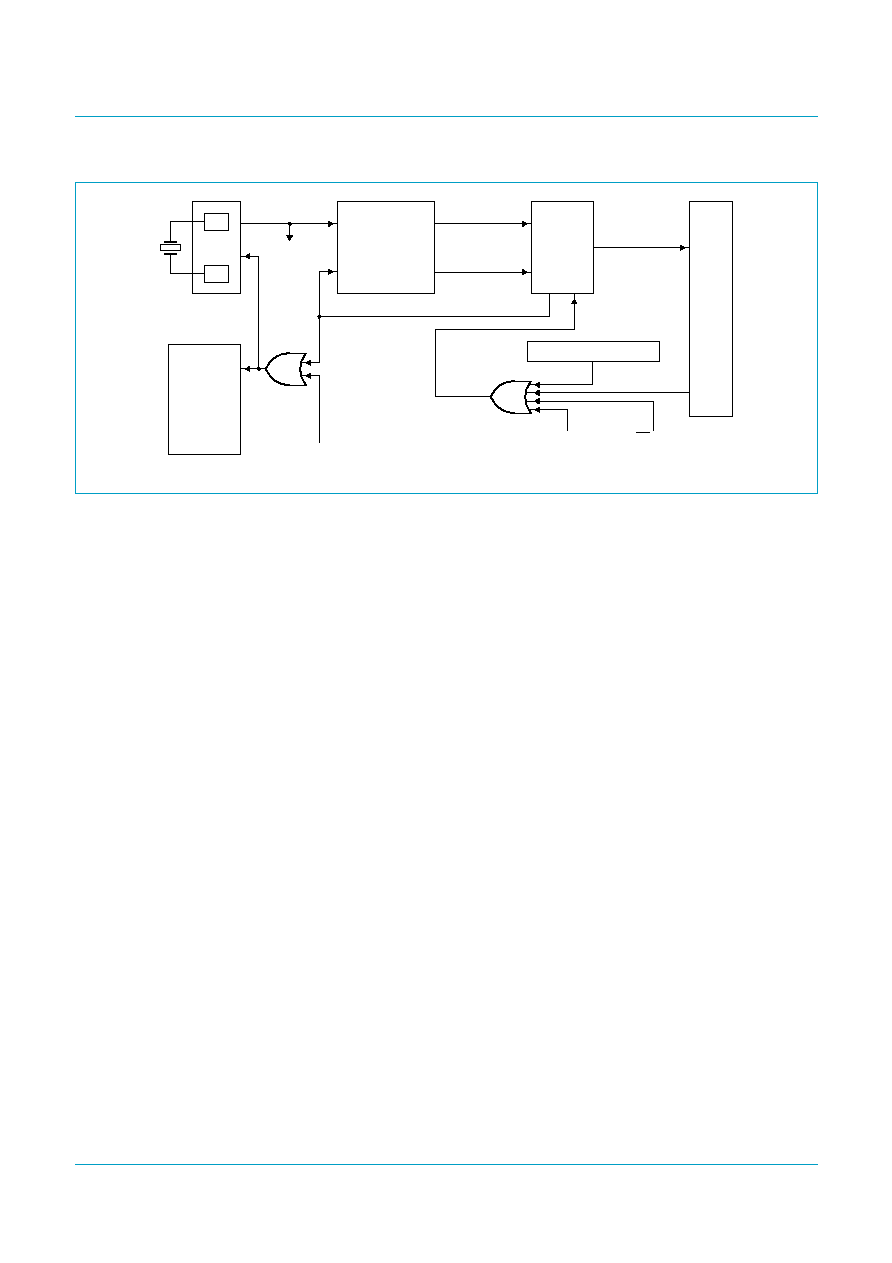
Philips Semiconductors
ISP1161A1
USB single-chip host and device controller
Product data
Rev. 03 -- 23 December 2004
42 of 136
9397 750 13961
© Koninklijke Philips Electronics N.V. 2004. All rights reserved.
In the suspended state, the device will consume considerably less power by turning
off the internal 48 MHz clock, PLL and crystal, and setting the internal regulator to
power-down mode. The ISP1161A1 suspend and resume clock scheme is shown in
Figure 37
.
Remark: The ISP1161A1 can only be put into a fully suspended state only after both
the HC and the DC go into the suspend state. At this point, the crystal can be turned
off and the internal regulator can be put into power-down mode.
Pin H_SUSPEND is the sensing output pin for the HC's suspended state. When
the HC goes into the USBSuspend state, this pin will output a HIGH level (logic 1).
This pin is cleared to LOW (logic 0) level only when the HC is put into a USBReset
state or USBOperational state (refer to the HcControl register bits 7 to 6, 01H to read,
81H to write). Bit 11, SuspendClkNotStop, of the HcHardwareConfiguration register
(20H to read, A0H to write), defines if the HC internal clock is stopped or kept running
when the HC goes into the USBSuspend state. After the HC enters the USBSuspend
state for 1.3 ms, the internal clock will be stopped if bit SuspendClkNotStop is logic 0.
9.9.2
HC wake-up from suspended state
There are three methods to wake up the HC from the USBSuspend state: hardware
wake-up, software wake-up, and USB bus resume. They are described as follows:
Wake-up by pin H_WAKEUP:
Pins H_SUSPEND and H_WAKEUP provide
hardware wake-up, a way of remote wake-up control for the HC without the need to
access the HC internal registers. H_WAKEUP is an external wake-up control input
pin for the HC. After the HC goes into the USBSuspend state, it can be woken up by
sending a HIGH level pulse to pin H_WAKEUP. This will turn on the HC's internal
clock, and set bit 6, ClkReady, of the Hc
µ
PInterrupt register (24H to read, A4H to
write). Under the USBSuspend state, once pin H_WAKEUP goes HIGH, after 160
µ
s,
the internal clock will be up. If pin H_WAKEUP continues to be HIGH, then the
internal clock will be kept running, and the microprocessor can set the HC into the
USBOperational state during this time. If H_WAKEUP goes LOW for more than
1.14 ms, the internal clock stops, and the HC goes back into the USBSuspend state.
Fig 37. ISP1161A1 suspend and resume clock scheme.
MGT958
On
On
XOSC_6MHz
(to DC PLL)
XOSC
On
VOLTAGE
REGULATOR
HC PLL
HC_ClkOk
HC_RawClk48M
HC_EnableClock
H_Wakeup (pin)
DC_EnableClock
CS (pin)
HC_NeedClock
PLL_Lock
PLL_ClkOut
On
DIGITAL
CLOCK
SWITCH
HC
CORE
HC_Clk48MOut
HcHardware Configuration
bit 11 (SuspendClkNotStop)

Philips Semiconductors
ISP1161A1
USB single-chip host and device controller
Product data
Rev. 03 -- 23 December 2004
43 of 136
9397 750 13961
© Koninklijke Philips Electronics N.V. 2004. All rights reserved.
Wake-up by pin CS (software wake-up):
During the USBSuspend state, an
external microprocessor issues a chip select signal through pin CS. This method of
access to the ISP1161A1 internal registers is a software wake-up.
Wake-up by USB devices:
For a USB bus resume, a USB device attached to the
root hub port issues a resume signal to the HC through the USB bus, switching
the HC from the USBSuspend state to the USBResume state. This will also set
bit ResumeDetected of the HcInterruptStatus register (03H to read, 83H to write).
No matter which method is used to wake up the HC from the USBSuspend state, the
corresponding interrupt bits must be enabled before the HC goes into the
USBSuspend state so that the microprocessor can receive the correct interrupt
request to wake up the HC.

Philips Semiconductors
ISP1161A1
USB single-chip host and device controller
Product data
Rev. 03 -- 23 December 2004
44 of 136
9397 750 13961
© Koninklijke Philips Electronics N.V. 2004. All rights reserved.
10. HC registers
The HC contains a set of on-chip control registers. These registers can be read or
written by the Host Controller Driver (HCD). The Control and Status register sets,
Frame Counter register sets, and Root Hub register sets are grouped under the
category of HC Operational registers (32 bits). These operational registers are made
compatible to OpenHCI (Host Controller Interface) Operational registers. This allows
the OpenHCI HCD to be easily ported to the ISP1161A1.
Reserved bits may be defined in future releases of this specification. To ensure
interoperability, the HCD must not assume that a reserved field contains logic 0.
Furthermore, the HCD must always preserve the values of the reserved field. When a
R/W register is modified, the HCD must first read the register, modify the bits desired,
and then write the register with the reserved bits still containing the original value.
Alternatively, the HCD can maintain an in-memory copy of previously written values
that can be modified and then written to the HC register. When a `write to set' or `clear
the register' is performed, bits written to reserved fields must be logic 0.
As shown in
Table 7
, the addresses (the commands for accessing registers) of these
32-bit Operational registers are similar to the offsets defined in the OHCI specification
with the addresses being equal to offset divided by 4.
Table 7:
HC Control register summary
Command (Hex)
Register
Width Reference
Functionality
read
write
00
-
HcRevision
32
Section 10.1.1 on page 45
HC Control and Status registers
01
81
HcControl
32
Section 10.1.2 on page 46
02
82
HcCommandStatus
32
Section 10.1.3 on page 47
03
83
HcInterruptStatus
32
Section 10.1.4 on page 48
04
84
HcInterruptEnable
32
Section 10.1.5 on page 49
05
85
HcInterruptDisable
32
Section 10.1.6 on page 51
0D
8D
HcFmInterval
32
Section 10.2.1 on page 52
HC Frame Counter registers
0E
-
HcFmRemaining
32
Section 10.2.2 on page 53
0F
-
HcFmNumber
32
Section 10.2.3 on page 54
11
91
HcLSThreshold
32
Section 10.2.4 on page 55
12
92
HcRhDescriptorA
32
Section 10.3.1 on page 56
HC Root Hub registers
13
93
HcRhDescriptorB
32
Section 10.3.2 on page 58
14
94
HcRhStatus
32
Section 10.3.3 on page 59
15
95
HcRhPortStatus[1]
32
Section 10.3.4 on page 61
16
96
HcRhPortStatus[2]
32
Section 10.3.4 on page 61
20
A0
HcHardwareConfiguration
16
Section 10.4.1 on page 65
HC DMA and Interrupt Control
registers
21
A1
HcDMAConfiguration
16
Section 10.4.2 on page 66
22
A2
HcTransferCounter
16
Section 10.4.3 on page 67
24
A4
Hc
µ
PInterrupt
16
Section 10.4.4 on page 68
25
A5
Hc
µ
PInterruptEnable
16
Section 10.4.5 on page 69

Philips Semiconductors
ISP1161A1
USB single-chip host and device controller
Product data
Rev. 03 -- 23 December 2004
45 of 136
9397 750 13961
© Koninklijke Philips Electronics N.V. 2004. All rights reserved.
10.1 HC control and status registers
10.1.1
HcRevision register (R: 00H)
Code (Hex): 00 -- read only
27
-
HcChipID
16
Section 10.5.1 on page 70
HC Miscellaneous registers
28
A8
HcScratch
16
Section 10.5.2 on page 71
-
A9
HcSoftwareReset
16
Section 10.5.3 on page 71
2A
AA
HcITLBufferLength
16
Section 10.6.1 on page 72
HC Buffer RAM Control registers
2B
AB
HcATLBufferLength
16
Section 10.6.2 on page 72
2C
-
HcBufferStatus
16
Section 10.6.3 on page 73
2D
-
HcReadBackITL0Length
16
Section 10.6.4 on page 74
2E
-
HcReadBackITL1Length
16
Section 10.6.5 on page 74
40
C0
HcITLBufferPort
16
Section 10.6.6 on page 75
41
C1
HcATLBufferPort
16
Section 10.6.7 on page 75
Table 7:
HC Control register summary
...continued
Command (Hex)
Register
Width Reference
Functionality
read
write
Table 8:
HcRevision register: bit allocation
Bit
31
30
29
28
27
26
25
24
Symbol
reserved
Reset
00H
Access
R
Bit
23
22
21
20
19
18
17
16
Symbol
reserved
Reset
00H
Access
R
Bit
15
14
13
12
11
10
9
8
Symbol
reserved
Reset
00H
Access
R
Bit
7
6
5
4
3
2
1
0
Symbol
REV[7:0]
Reset
10H
Access
R
Table 9:
HcRevision register: bit description
Bit
Symbol
Description
31 to 8
-
Reserved
7 to 0
REV[7:0]
Revision: This read-only field contains the BCD representation of
the version of the HCI specification that is implemented by this HC.
For example, a value of 11H corresponds to version 1.1. All HC
implementations that are compliant with this specification will have
a value of 10H.

Philips Semiconductors
ISP1161A1
USB single-chip host and device controller
Product data
Rev. 03 -- 23 December 2004
46 of 136
9397 750 13961
© Koninklijke Philips Electronics N.V. 2004. All rights reserved.
10.1.2
HcControl register (R/W: 01H/81H)
The HcControl register defines the operating modes for the HC.
RemoteWakeupEnable (RWE) is modified only by the HCD.
Code (Hex): 01 -- read
Code (Hex): 81 -- write
Table 10:
HcControl register: bit allocation
Bit
31
30
29
28
27
26
25
24
Symbol
reserved
Reset
00H
Access
R/W
Bit
23
22
21
20
19
18
17
16
Symbol
reserved
Reset
00H
Access
R/W
Bit
15
14
13
12
11
10
9
8
Symbol
reserved
RWE
RWC
reserved
Reset
0
0
0
0
0
0
0
0
Access
R/W
R/W
R/W
R/W
R/W
R/W
R/W
R/W
Bit
7
6
5
4
3
2
1
0
Symbol
HCFS[1:0]
reserved
Reset
0
0
0
0
0
0
0
0
Access
R/W
R/W
R/W
R/W
R/W
R/W
R/W
R/W
Table 11:
HcControl register: bit description
Bit
Symbol
Description
31 to 11
-
reserved
10
RWE
RemoteWakeupEnable: This bit is used by the HCD to enable or
disable the remote wake-up feature upon the detection of
upstream resume signaling. When this bit is set and the
ResumeDetected bit in HcInterruptStatus is set, a remote wake-up
is signaled to the host system. Setting this bit has no impact on the
generation of hardware interrupt.
9
RWC
RemoteWakeupConnected: This bit indicates whether the HC
supports remote wake-up signaling. If remote wake-up is
supported and used by the system, it is the responsibility of
system firmware to set this bit during POST. The HC clears the bit
upon a hardware reset but does not alter it upon a software reset.
Remote wake-up signaling of the host system is host-bus-specific,
and is not described in this specification.

Philips Semiconductors
ISP1161A1
USB single-chip host and device controller
Product data
Rev. 03 -- 23 December 2004
47 of 136
9397 750 13961
© Koninklijke Philips Electronics N.V. 2004. All rights reserved.
10.1.3
HcCommandStatus register (R/W: 02H/82H)
The HcCommandStatus register is used by the HC to receive commands issued by
the HCD, and it also reflects the HC's current status. To the HCD, it appears to be a
`write to set' register. The HC must ensure that bits written as logic 1 become set in
the register while bits written as logic 0 remain unchanged in the register. The HCD
may issue multiple distinct commands to the HC without concern for corrupting
previously issued commands. The HCD has normal read access to all bits.
The SchedulingOverrunCount field indicates the number of frames with which the HC
has detected the scheduling overrun error. This occurs when the Periodic list does
not complete before EOF. When a scheduling overrun error is detected, the HC
increments the counter and sets the SchedulingOverrun field in the HcInterruptStatus
register.
Code (Hex): 02 -- read
Code (Hex): 82 -- write
8
-
reserved
7 to 6
HCFS
HostControllerFunctionalState for USB:
00B -- USBReset
01B -- USBResume
10B -- USBOperational
11B -- USBSuspend
A transition to USBOperational from another state causes
start-of-frame (SOF) generation to begin 1 ms later. The HCD
determines whether the HC has begun sending SOFs by reading
the StartofFrame field of HcInterruptStatus.
This field can be changed by the HC only when in the
USBSuspend state. The HC can move from the USBSuspend
state to the USBResume state after detecting the resume signaling
from a downstream port.
The HC enters USBReset after a software reset and a hardware
reset. The latter also resets the Root Hub and asserts subsequent
reset signaling to downstream ports.
5 to 0
-
reserved
Table 11:
HcControl register: bit description
...continued
Bit
Symbol
Description
Table 12:
HcCommandStatus register: bit allocation
Bit
31
30
29
28
27
26
25
24
Symbol
reserved
Reset
00H
Access
R
Bit
23
22
21
20
19
18
17
16
Symbol
reserved
SOC[1:0]
Reset
0
0
0
0
0
0
0
0
Access
R
R
R
R
R
R
R
R

Philips Semiconductors
ISP1161A1
USB single-chip host and device controller
Product data
Rev. 03 -- 23 December 2004
48 of 136
9397 750 13961
© Koninklijke Philips Electronics N.V. 2004. All rights reserved.
10.1.4
HcInterruptStatus register (R/W: 03H/83H)
This register provides the status of the events that cause hardware interrupts. When
an event occurs, the HC sets the corresponding bit in this register. When a bit is set, a
hardware interrupt is generated if the interrupt is enabled in the HcInterruptEnable
register (see
Section 10.1.5
) and bit MasterInterruptEnable is set. The HCD can clear
individual bits in this register by writing logic 1 to the bit positions to be cleared, but
cannot set any of these bits. Conversely, the HC can set bits in this register, but
cannot clear the bits.
Code (Hex): 03 -- read
Code (Hex): 83 -- write
Bit
15
14
13
12
11
10
9
8
Symbol
reserved
Reset
00H
Access
R/W
Bit
7
6
5
4
3
2
1
0
Symbol
reserved
HCR
Reset
0
0
0
0
0
0
0
0
Access
R/W
R/W
R/W
R/W
R/W
R/W
R/W
R/W
Table 13:
HcCommandStatus register: bit description
Bit
Symbol
Description
31 to 18
-
reserved
17 to 16
SOC[1:0]
SchedulingOverrunCount: The field is incremented on each
scheduling overrun error. It is initialized to 00B and wraps around
at 11B. It will be incremented when a scheduling overrun is
detected even if SchedulingOverrun in HcInterruptStatus has
already been set. This is used by HCD to monitor any persistent
scheduling problems.
15 to 1
-
reserved
0
HCR
HostControllerReset: This bit is set by the HCD to initiate a
software reset of the HC. Regardless of the functional state of
the HC, it moves to the USBSuspend state in which most of the
operational registers are reset, except those stated otherwise, and
no Host bus accesses are allowed. This bit is cleared by the HC
upon the completion of the reset operation. The reset operation
must be completed within 10
µ
s. This bit, when set, does not
cause a reset to the Root Hub and no subsequent reset signaling
will be asserted to its downstream ports.
Table 14:
HcInterruptStatus register: bit allocation
Bit
31
30
29
28
27
26
25
24
Symbol
reserved
Reset
00H
Access
R/W

Philips Semiconductors
ISP1161A1
USB single-chip host and device controller
Product data
Rev. 03 -- 23 December 2004
49 of 136
9397 750 13961
© Koninklijke Philips Electronics N.V. 2004. All rights reserved.
10.1.5
HcInterruptEnable register (R/W: 04H/84H)
Each enable bit in the HcInterruptEnable register corresponds to an associated
interrupt bit in the HcInterruptStatus register. The HcInterruptEnable register is used
to control which events generate a hardware interrupt. A hardware interrupt is
requested on the host bus when three conditions occur:
·
A bit is set in the HcInterruptStatus register
·
The corresponding bit in the HcInterruptEnable register is set
·
Bit MasterInterruptEnable is set.
Bit
23
22
21
20
19
18
17
16
Symbol
reserved
Reset
00H
Access
R/W
Bit
15
14
13
12
11
10
9
8
Symbol
reserved
Reset
00H
Access
R/W
Bit
7
6
5
4
3
2
1
0
Symbol
reserved
RHSC
FNO
UE
RD
SF
reserved
SO
Reset
0
0
0
0
0
0
0
0
Access
R/W
R/W
R/W
R/W
R/W
R/W
R/W
R/W
Table 15:
HcInterruptStatus register: bit description
Bit
Symbol
Description
31 to 7
-
reserved
6
RHSC
RootHubStatusChange: This bit is set when the content of
HcRhStatus or the content of any of HcRhPortStatus[1:2] has
changed.
5
FNO
FrameNumberOverflow: This bit is set when the MSB of
HcFmNumber (bit 15) changes value.
4
UE
UnrecoverableError: This bit is set when the HC detects a
system error not related to USB. The HC does not proceed with
any processing nor signaling before the system error has been
corrected. The HCD clears this bit after the HC has been reset.
OHCI: Always set to logic 0.
3
RD
ResumeDetected: This bit is set when the HC detects that a
device on the USB is asserting resume signaling from a state of no
resume signaling. This bit is not set when HCD enters the
USBResume state.
2
SF
StartofFrame: At the start of each frame, this bit is set by the HC
and an SOF is generated.
1
-
reserved
0
SO
SchedulingOverrun: This bit is set when the USB schedules for
current frame overruns. A scheduling overrun will also cause the
SchedulingOverrunCount of HcCommandStatus to be
incremented.

Philips Semiconductors
ISP1161A1
USB single-chip host and device controller
Product data
Rev. 03 -- 23 December 2004
50 of 136
9397 750 13961
© Koninklijke Philips Electronics N.V. 2004. All rights reserved.
Writing a logic 1 to a bit in this register sets the corresponding bit, whereas writing a
logic 0 to a bit in this register leaves the corresponding bit unchanged. On a read, the
current value of this register is returned.
Code (Hex): 04 -- read
Code (Hex): 84 -- write
Table 16:
HcInterruptEnable register: bit allocation
Bit
31
30
29
28
27
26
25
24
Symbol
MIE
reserved
Reset
0
0
0
0
0
0
0
0
Access
R/W
R/W
R/W
R/W
R/W
R/W
R/W
R/W
Bit
23
22
21
20
19
18
17
16
Symbol
reserved
Reset
00H
Access
R/W
Bit
15
14
13
12
11
10
9
8
Symbol
reserved
Reset
00H
Access
R/W
Bit
7
6
5
4
3
2
1
0
Symbol
reserved
RHSC
FNO
UE
RD
SF
reserved
SO
Reset
0
0
0
0
0
0
0
0
Access
R/W
R/W
R/W
R/W
R/W
R/W
R/W
R/W
Table 17:
HcInterruptEnable register: bit description
Bit
Symbol
Description
31
MIE
MasterInterruptEnable by the HCD: A logic 0 is ignored by
the HC. A logic 1 enables interrupt generation by events specified
in other bits of this register.
30 to 7
-
reserved
6
RHSC
0 -- ignore
1 -- enable interrupt generation due to Root Hub Status Change
5
FNO
0 -- ignore
1 -- enable interrupt generation due to Frame Number Overflow
4
UE
0 -- ignore
1 -- enable interrupt generation due to Unrecoverable Error
3
RD
0 -- ignore
1 -- enable interrupt generation due to Resume Detect
2
SF
0 -- ignore
1 -- enable interrupt generation due to Start of Frame
1
-
reserved
0
SO
0 -- ignore
1 -- enable interrupt generation due to Scheduling Overrun

Philips Semiconductors
ISP1161A1
USB single-chip host and device controller
Product data
Rev. 03 -- 23 December 2004
51 of 136
9397 750 13961
© Koninklijke Philips Electronics N.V. 2004. All rights reserved.
10.1.6
HcInterruptDisable register (R/W: 05H/85H)
Each disable bit in the HcInterruptDisable register corresponds to an associated
interrupt bit in the HcInterruptStatus register. The HcInterruptDisable register is
coupled with the HcInterruptEnable register. Thus, writing a logic 1 to a bit in this
register clears the corresponding bit in the HcInterruptEnable register, whereas
writing a logic 0 to a bit in this register leaves the corresponding bit in the
HcInterruptEnable register unchanged. On a read, the current value of the
HcInterruptEnable register is returned.
Code (Hex): 05 -- read
Code (Hex): 85 -- write
Table 18:
HcInterruptDisable register: bit allocation
Bit
31
30
29
28
27
26
25
24
Symbol
MIE
reserved
Reset
0
0
0
0
0
0
0
0
Access
R/W
R/W
R/W
R/W
R/W
R/W
R/W
R/W
Bit
23
22
21
20
19
18
17
16
Symbol
reserved
Reset
00H
Access
R/W
Bit
15
14
13
12
11
10
9
8
Symbol
reserved
Reset
00H
Access
R/W
Bit
7
6
5
4
3
2
1
0
Symbol
reserved
RHSC
FNO
UE
RD
SF
reserved
SO
Reset
0
0
0
0
0
0
0
0
Access
R/W
R/W
R/W
R/W
R/W
R/W
R/W
R/W
Table 19:
HcInterruptDisable register: bit description
Bit
Symbol
Description
31
MIE
A logic 0 is ignored by the HC. A logic 1 disables interrupt
generation due to events specified in other bits of this register. This
bit is set after a hardware or software reset.
30 to 7
-
reserved
6
RHSC
0 -- ignore
1 -- disable interrupt generation due to Root Hub Status Change

Philips Semiconductors
ISP1161A1
USB single-chip host and device controller
Product data
Rev. 03 -- 23 December 2004
52 of 136
9397 750 13961
© Koninklijke Philips Electronics N.V. 2004. All rights reserved.
10.2 HC frame counter registers
10.2.1
HcFmInterval register (R/W: 0DH/8DH)
The HcFmInterval register contains a 14-bit value which indicates the bit time interval
in a frame (that is, between two consecutive SOFs), and a 15-bit value indicating the
full-speed maximum packet size that the HC may transmit or receive without causing
a scheduling overrun. The HCD may carry out minor adjustments on the
FrameInterval by writing a new value at each SOF. This allows the HC to synchronize
with an external clock source and to adjust any unknown clock offset.
Code (Hex): 0D -- read
Code (Hex): 8D -- write
5
FNO
0 -- ignore
1 -- disable interrupt generation due to Frame Number Overflow
4
UE
0 -- ignore
1 -- disable interrupt generation due to Unrecoverable Error
3
RD
0 -- ignore
1 -- disable interrupt generation due to Resume Detect
2
SF
0 -- ignore
1 -- disable interrupt generation due to Start of Frame
1
-
reserved
0
SO
0 -- ignore
1 -- disable interrupt generation due to Scheduling Overrun
Table 19:
HcInterruptDisable register: bit description
...continued
Bit
Symbol
Description
Table 20:
HcFmInterval register: bit allocation
Bit
31
30
29
28
27
26
25
24
Symbol
FIT
FSMPS[14:8]
Reset
0
0
0
0
0
0
0
0
Access
R/W
R/W
R/W
R/W
R/W
R/W
R/W
R/W
Bit
23
22
21
20
19
18
17
16
Symbol
FSMPS[7:0]
Reset
00H
Access
R/W
Bit
15
14
13
12
11
10
9
8
Symbol
reserved
FI[13:8]
Reset
0
0
1
0
1
1
1
0
Access
R/W
R/W
R/W
R/W
R/W
R/W
R/W
R/W
Bit
7
6
5
4
3
2
1
0
Symbol
FI[7:0]
Reset
DFH
Access
R/W

Philips Semiconductors
ISP1161A1
USB single-chip host and device controller
Product data
Rev. 03 -- 23 December 2004
53 of 136
9397 750 13961
© Koninklijke Philips Electronics N.V. 2004. All rights reserved.
10.2.2
HcFmRemaining register (R: 0EH)
The HcFmRemaining register is a 14-bit down counter showing the bit time remaining
in the current frame.
Code (Hex): 0E -- read
Table 21:
HcFmInterval register: bit description
Bit
Symbol
Description
31
FIT
FrameIntervalToggle: The HCD toggles this bit whenever it loads
a new value to FrameInterval.
30 to 16
FSMPS
[14:0]
FSLargestDataPacket (FSMaxPacketSize): Specifies a value
which is loaded into the Largest Data Packet Counter at the
beginning of each frame. The counter value represents the largest
amount of data in bits which can be sent or received by the HC in a
single transaction at any given time without causing a scheduling
overrun. The field value is calculated by the HCD.
15 to 14
-
reserved
13 to 0
FI[13:0]
FrameInterval: Specifies the interval between two consecutive
SOFs in bit times. The default value is 11999. The HCD must save
the current value of this field before resetting the HC. Setting the
HostControllerReset field of the HcCommandStatus register will
cause the HC to reset this field to its default value. HCD may
choose to restore the saved value upon completing the reset
sequence.
Table 22:
HcFmRemaining register: bit allocation
Bit
31
30
29
28
27
26
25
24
Symbol
FRT
reserved
Reset
0
0
0
0
0
0
0
0
Access
R
R
R
R
R
R
R
R
Bit
23
22
21
20
19
18
17
16
Symbol
reserved
Reset
00H
Access
R
Bit
15
14
13
12
11
10
9
8
Symbol
reserved
FR[13:8]
Reset
0
0
0
0
0
0
0
0
Access
R
R
R
R
R
R
R
R
Bit
7
6
5
4
3
2
1
0
Symbol
FR[7:0]
Reset
00H
Access
R

Philips Semiconductors
ISP1161A1
USB single-chip host and device controller
Product data
Rev. 03 -- 23 December 2004
54 of 136
9397 750 13961
© Koninklijke Philips Electronics N.V. 2004. All rights reserved.
10.2.3
HcFmNumber register (R: 0FH)
The HcFmNumber register is a 16-bit counter. It provides a timing reference for
events happening in the HC and the HCD. The HCD may use the 16-bit value
specified in this register and generate a 32-bit frame number without requiring
frequent access to the register.
Code (Hex): 0F -- read
Table 23:
HcFmRemaining register: bit description
Bit
Symbol
Description
31
FRT
FrameRemainingToggle: This bit is loaded from the
FrameIntervalToggle field of the HcFmInterval register whenever
FrameRemaining reaches 0. This bit is used by the HCD for
synchronization between FrameInterval and FrameRemaining.
30 to 14
-
reserved
13 to 0
FR[13:0]
FrameRemaining: This counter is decremented at each bit time.
When it reaches zero, it is reset by loading the FrameInterval value
specified in the HcFmInterval register at the next bit time boundary.
When entering the USBOperational state, the HC reloads it with
the content of the FrameInterval part of the HcFmInterval register
and uses the updated value from the next SOF.
Table 24:
HCFmNumber register: bit allocation
Bit
31
30
29
28
27
26
25
24
Symbol
reserved
Reset
00H
Access
R
Bit
23
22
21
20
19
18
17
16
Symbol
reserved
Reset
00H
Access
R
Bit
15
14
13
12
11
10
9
8
Symbol
FN[15:8]
Reset
00H
Access
R
Bit
7
6
5
4
3
2
1
0
Symbol
FN[7:0]
Reset
00H
Access
R
Table 25:
HcFmNumber register: bit description
Bit
Symbol
Description
31 to 16
-
reserved
15 to 0
FN[15:0]
FrameNumber: This field is incremented when HcFmRemaining
is reloaded. It rolls over to 0000H after FFFFH. When the
USBOperational state is entered, this field will be incremented
automatically. The HC will set bit StartofFrame in the
HcInterruptStatus register.

Philips Semiconductors
ISP1161A1
USB single-chip host and device controller
Product data
Rev. 03 -- 23 December 2004
55 of 136
9397 750 13961
© Koninklijke Philips Electronics N.V. 2004. All rights reserved.
10.2.4
HcLSThreshold register (R/W: 11H/91H)
The HcLSThreshold register contains an 11-bit value used by the HC to determine
whether to commit to the transfer of a maximum of 8-byte LS packet before EOF.
Neither the HC nor the HCD is allowed to change this value.
Code (Hex): 11 -- read
Code (Hex): 91 -- write
10.3 HC Root Hub registers
All registers included in this partition are dedicated to the USB Root Hub, which is an
integral part of the HC although it is functionally a separate entity. The Host Controller
Driver (HCD) emulates USBD accesses to the Root Hub via a register interface. The
HCD maintains many USB-defined hub features that are not required to be supported
in hardware. For example, the Hub's Device, Configuration, Interface, Endpoint
Descriptors, as well as some static fields of the Class Descriptor, are maintained only
in the HCD. The HCD also maintains and decodes the Root Hub's device address as
well as other minor operations more suited for software than for hardware.
The Root Hub registers were developed to match the bit organization and operation
of typical hubs found in the system.
Table 26:
HcLSThreshold register: bit allocation
Bit
31
30
29
28
27
26
25
24
Symbol
reserved
Reset
00H
Access
R/W
Bit
23
22
21
20
19
18
17
16
Symbol
reserved
Reset
00H
Access
R/W
Bit
15
14
13
12
11
10
9
8
Symbol
reserved
LST[10:8]
Reset
0
0
0
0
0
1
1
0
Access
R/W
R/W
R/W
R/W
R/W
R/W
R/W
R/W
Bit
7
6
5
4
3
2
1
0
Symbol
LST[7:0]
Reset
28H
Access
R/W
Table 27:
HcLSThreshold register: bit description
Bit
Symbol
Description
31 to 11
-
reserved
10 to 0
LST[10:0]
LSThreshold: Contains a value that is compared to the
FrameRemaining field before a low-speed transaction is initiated.
The transaction is started only if FrameRemaining
this field. The
value is calculated by the HCD, which considers transmission and
set-up overhead. Default value: 1576 (628H)

Philips Semiconductors
ISP1161A1
USB single-chip host and device controller
Product data
Rev. 03 -- 23 December 2004
56 of 136
9397 750 13961
© Koninklijke Philips Electronics N.V. 2004. All rights reserved.
Four 32-bit registers have been defined:
·
HcRhDescriptorA
·
HcRhDescriptorB
·
HcRhStatus
·
HcRhPortStatus[1:NDP]
Each register is read and written as a DWORD. These registers are only written
during initialization to correspond with the system implementation. The
HcRhDescriptorA and HcRhDescriptorB registers are writeable regardless of the
HC's USB states. HcRhStatus and HcRhPortStatus are writeable during the
USBOperational state only.
10.3.1
HcRhDescriptorA register (R/W: 12H/92H)
The HcRhDescriptorA register is the first register of two describing the characteristics
of the Root Hub. Reset values are Implementation-Specific (IS). The descriptor length
(11), descriptor type and hub controller current (0) fields of the hub Class Descriptor
are emulated by the HCD. All other fields are located in registers HcRhDescriptorA
and HcRhDescriptorB.
Remark: IS denotes an implementation-specific reset value for that field.
Code (Hex): 12 -- read
Code (Hex): 92 -- write
Table 28:
HcRhDescriptorA register: bit description
Bit
31
30
29
28
27
26
25
24
Symbol
POTPGT[7:0]
Reset
IS
Access
R/W
Bit
23
22
21
20
19
18
17
16
Symbol
reserved
Reset
00H
Access
R/W
Bit
15
14
13
12
11
10
9
8
Symbol
reserved
NOCP
OCPM
DT
NPS
PSM
Reset
0
0
0
IS
IS
0
IS
IS
Access
R
R
R
R/W
R/W
R
R/W
R/W
Bit
7
6
5
4
3
2
1
0
Symbol
reserved
NDP[1:0]
Reset
0
0
0
0
0
0
IS
IS
Access
R
R
R
R
R
R
R
R

Philips Semiconductors
ISP1161A1
USB single-chip host and device controller
Product data
Rev. 03 -- 23 December 2004
57 of 136
9397 750 13961
© Koninklijke Philips Electronics N.V. 2004. All rights reserved.
Table 29:
HcRhDescriptorA register: bit description
Bit
Symbol
Description
31 to 24
POTPGT
[7:0]
PowerOnToPowerGoodTime: This byte specifies the duration
HCD has to wait before accessing a powered-on port of the Root
Hub. The unit of time is 2 ms. The duration is calculated as
POTPGT
×
2 ms.
23 to 13
-
reserved
12
NOCP
NoOverCurrentProtection: This bit describes how the
overcurrent status for the Root Hub ports are reported. When this
bit is cleared, the OverCurrentProtectionMode field specifies
global or per-port reporting.
0 -- overcurrent status is reported collectively for all downstream
ports
1 -- no overcurrent reporting supported
11
OCPM
OverCurrentProtectionMode: This bit describes how the
overcurrent status for the Root Hub ports is reported. At reset, this
field reflects the same mode as PowerSwitchingMode. This field is
valid only if the NoOverCurrentProtection field is cleared.
0 -- overcurrent status is reported collectively for all downstream
ports.
1 -- overcurrent status is reported on a per-port basis. On
power-up, clear this bit and then set it to logic 1.
10
DT
DeviceType: This bit specifies that the Root Hub is not a
compound device--it is not permitted. This field will always
read/write 0.
9
NPS
NoPowerSwitching: This bit is used to specify whether power
switching is supported or ports are always powered. It is
implementation-specific. When this bit is cleared, the bit
PowerSwitchingMode specifies global or per-port switching.
0 -- ports are power switched
1 -- ports are always powered on when the HC is powered on
8
PSM
PowerSwitchingMode: This bit is used to specify how the power
switching of the Root Hub ports is controlled. It is
implementation-specific. This field is valid only if the
NoPowerSwitching field is cleared.
0 -- all ports are powered at the same time
1 -- each port is powered individually. This mode allows port
power to be controlled by either the global switch or per-port
switching. If bit PortPowerControlMask is set, the port responds to
only port power commands (Set/ClearPortPower). If the port mask
is cleared, then the port is controlled only by the global power
switch (Set/ClearGlobalPower).
7 to 2
-
reserved
1 to 0
NDP[1:0]
NumberDownstreamPorts: These bits specify the number of
downstream ports supported by the Root Hub. The maximum
number of ports supported by the ISP1161A1 is 2.

Philips Semiconductors
ISP1161A1
USB single-chip host and device controller
Product data
Rev. 03 -- 23 December 2004
58 of 136
9397 750 13961
© Koninklijke Philips Electronics N.V. 2004. All rights reserved.
10.3.2
HcRhDescriptorB register (R/W: 13H/93H)
The HcRhDescriptorB register is the second register of two describing the
characteristics of the Root Hub. These fields are written during initialization to
correspond with the system implementation. Reset values are
implementation-specific (IS).
Code (Hex): 13 -- read
Code (Hex): 93 -- write
Table 30:
HcRhDescriptorB register: bit allocation
Bit
31
30
29
28
27
26
25
24
Symbol
reserved
Reset
N/A
Access
R
Bit
23
22
21
20
19
18
17
16
Symbol
reserved
PPCM[2:0]
Reset
N/A
N/A
N/A
N/A
N/A
IS
IS
IS
Access
R
R
R
R
R
R/W
R/W
R/W
Bit
15
14
13
12
11
10
9
8
Symbol
reserved
Reset
N/A
Access
R
Bit
7
6
5
4
3
2
1
0
Symbol
reserved
DR[2:0]
Reset
N/A
N/A
N/A
N/A
N/A
IS
IS
IS
Access
R
R
R
R
R
R/W
R/W
R/W

Philips Semiconductors
ISP1161A1
USB single-chip host and device controller
Product data
Rev. 03 -- 23 December 2004
59 of 136
9397 750 13961
© Koninklijke Philips Electronics N.V. 2004. All rights reserved.
10.3.3
HcRhStatus register (R/W: 14H/94H)
The HcRhStatus register is divided into two parts. The lower word of a DWORD
represents the Hub Status field and the upper word represents the Hub Status
Change field. Reserved bits should always be written as logic 0.
Code (Hex): 14 -- read
Code (Hex): 94 -- write
Table 31:
HcRhDescriptorB register: bit description
Bit
Symbol
Description
31 to 19
-
reserved
18 to 16
PPCM[2:0]
PortPowerControlMask: Each bit indicates whether a port is
affected by a global power control command when
PowerSwitchingMode is set. When set, the port's power state is
only affected by per-port power control (Set/ClearPortPower).
When cleared, the port is controlled by the global power switch
(Set/ClearGlobalPower). If the device is configured to global
switching mode (PowerSwitchingMode = 0), this field is not valid.
Bit 0 -- reserved
Bit 1 -- Ganged-power mask on Port #1
Bit 2 -- Ganged-power mask on Port #2
15 to 3
-
reserved
2 to 0
DR[2:0]
DeviceRemovable: Each bit is dedicated to a port of the Root
Hub. When cleared, the attached device is removable. When set,
the attached device is not removable.
Bit 0 -- reserved
Bit 1 -- Device attached to Port #1
Bit 2 -- Device attached to Port #2
Table 32:
HcRhStatus register: bit allocation
Bit
31
30
29
28
27
26
25
24
Symbol
CRWE
reserved
Reset
0
0
0
0
0
0
0
0
Access
W
R
R
R
R
R
R
R
Bit
23
22
21
20
19
18
17
16
Symbol
reserved
OCIC
LPSC
Reset
0
0
0
0
0
0
0
0
Access
R
R
R
R
R
R
R/W
R/W
Bit
15
14
13
12
11
10
9
8
Symbol
DRWE
reserved
Reset
0
0
0
0
0
0
0
0
Access
R/W
R
R
R
R
R
R
R

Philips Semiconductors
ISP1161A1
USB single-chip host and device controller
Product data
Rev. 03 -- 23 December 2004
60 of 136
9397 750 13961
© Koninklijke Philips Electronics N.V. 2004. All rights reserved.
Bit
7
6
5
4
3
2
1
0
Symbol
reserved
OCI
LPS
Reset
0
0
0
0
0
0
0
0
Access
R
R
R
R
R
R
R
R/W
Table 33:
HcRhStatus register: bit description
Bit
Symbol
Description
31
CRWE
On write--ClearRemoteWakeupEnable: Writing a logic 1 clears
DeviceRemoveWakeupEnable. Writing a logic 0 has no effect.
30 to 18
-
reserved
17
OCIC
OverCurrentIndicatorChange: This bit is set by hardware when a
change has occurred to the OCI field of this register. The HCD
clears this bit by writing a logic 1. Writing a logic 0 has no effect.
16
LPSC
On read--LocalPowerStatusChange: The Root Hub does not
support the local power status feature. Therefore, this bit is always
read as logic 0.
On write--SetGlobalPower: In global power mode
(PowerSwitchingMode=0), this bit is written to logic 1 to turn on
power to all ports (clear PortPowerStatus). In per-port power
mode, it sets PortPowerStatus only on ports whose bit
PortPowerControlMask is not set. Writing a logic 0 has no effect.
15
DRWE
On read--DeviceRemoteWakeupEnable: This bit enables the bit
ConnectStatusChange as a resume event, causing a state
transition USBSuspend to USBResume and setting the
ResumeDetected interrupt.
0 -- ConnectStatusChange is not a remote wake-up event
1 -- ConnectStatusChange is a remote wake-up event
On write--SetRemoteWakeupEnable: Writing a logic 1 sets
DeviceRemoveWakeupEnable. Writing a logic 0 has no effect.
14 to 2
-
reserved
1
OCI
OverCurrentIndicator: This bit reports overcurrent conditions
when global reporting is implemented. When set, an overcurrent
condition exists. When clear, all power operations are normal. If
per-port overcurrent protection is implemented this bit is always
logic 0.
0
LPS
On read--LocalPowerStatus: The Root Hub does not support the
local power status feature. Therefore, this bit is always read as
logic 0.
On write--ClearGlobalPower: In global power mode
(PowerSwitchingMode = 0), this bit is written to logic 1 to turn off
power to all ports (clear PortPowerStatus). In per-port power
mode, it clears PortPowerStatus only on ports whose
bit PortPowerControlMask is not set. Writing a logic 0 has no
effect.

Philips Semiconductors
ISP1161A1
USB single-chip host and device controller
Product data
Rev. 03 -- 23 December 2004
61 of 136
9397 750 13961
© Koninklijke Philips Electronics N.V. 2004. All rights reserved.
10.3.4
HcRhPortStatus[1:2] register (R/W [1]:15H/95H, [2]: 16H/96H)
The HcRhPortStatus[1:2] register is used to control and report port events on a
per-port basis. NumberDownstreamPorts represents the number of HcRhPortStatus
registers that are implemented in hardware. The lower word is used to reflect the port
status, whereas the upper word reflects the status change bits. Some status bits are
implemented with special write behavior. If a transaction (token through handshake)
is in progress when a write to change port status occurs, the resulting port status
change must be postponed until the transaction completes. Reserved bits should
always be written logic 0.
Code (Hex): [1] = 15, [2] = 16 -- read
Code (Hex): [1] = 95, [2] = 96 -- write
Table 34:
HcRhPortStatus[1:2] register: bit allocation
Bit
31
30
29
28
27
26
25
24
Symbol
reserved
Reset
00H
Access
R/W
Bit
23
22
21
20
19
18
17
16
Symbol
reserved
PRSC
OCIC
PSSC
PESC
CSC
Reset
0
0
0
0
0
0
0
0
Access
R/W
R/W
R/W
R/W
R/W
R/W
R/W
R/W
Bit
15
14
13
12
11
10
9
8
Symbol
reserved
LSDA
PPS
Reset
0
0
0
0
0
0
0
0
Access
R/W
R/W
R/W
R/W
R/W
R/W
R/W
R/W
Bit
7
6
5
4
3
2
1
0
Symbol
reserved
PRS
POCI
PSS
PES
CCS
Reset
0
0
0
0
0
0
0
0
Access
R/W
R/W
R/W
R/W
R/W
R/W
R/W
R/W
Table 35:
HcRhPortStatus[1:2] register: bit description
Bit
Symbol
Description
31 to 21
-
reserved
20
PRSC
PortResetStatusChange: This bit is set at the end of the 10 ms
port reset signal. The HCD writes a logic 1 to clear this bit. Writing
a logic 0 has no effect.
0 -- port reset is not complete
1 -- port reset is complete
19
OCIC
PortOverCurrentIndicatorChange: This bit is valid only if
overcurrent conditions are reported on a per-port basis. This bit is
set when Root Hub changes the PortOverCurrentIndicator bit. The
HCD writes a logic 1 to clear this bit. Writing a logic 0 has no
effect.
0 -- no change in PortOverCurrentIndicator
1 -- PortOverCurrentIndicator has changed

Philips Semiconductors
ISP1161A1
USB single-chip host and device controller
Product data
Rev. 03 -- 23 December 2004
62 of 136
9397 750 13961
© Koninklijke Philips Electronics N.V. 2004. All rights reserved.
18
PSSC
PortSuspendStatusChange: This bit is set when the full resume
sequence has been completed. This sequence includes the 20 s
resume pulse, LS EOP, and 3 ms resynchronization delay. The
HCD writes a logic 1 to clear this bit. Writing a logic 0 has no
effect. This bit is also cleared when ResetStatusChange is set.
0 -- resume is not complete
1 -- resume is complete
17
PESC
PortEnableStatusChange: This bit is set when hardware events
cause bit PortEnableStatus to be cleared. Changes from HCD
writes do not set this bit. The HCD writes a logic 1 to clear this bit.
Writing a logic 0 has no effect.
0 -- no change in PortEnableStatus
1 -- change in PortEnableStatus
16
CSC
ConnectStatusChange: This bit is set whenever a connect or
disconnect event occurs. The HCD writes a logic 1 to clear this bit.
Writing a logic 0 has no effect. If CurrentConnectStatus is cleared
when a SetPortReset, SetPortEnable, or SetPortSuspend write
occurs, this bit is set to force the driver to reevaluate the
connection status since these writes should not occur if the port is
disconnected.
0 -- no change in CurrentConnectStatus
1 -- change in CurrentConnectStatus
Remark: If bit DeviceRemovable[NDP] is set, this bit is set only
after a Root Hub reset to inform the system that the device is
connected.
15 to 10
-
reserved
9
LSDA
(read) LowSpeedDeviceAttached: This bit indicates the speed of
the device connected to this port. When set, a low-speed device is
connected to this port. When clear, a full-speed device is
connected to this port. This field is valid only when the
CurrentConnectStatus is set.
0 -- full-speed device attached
1 -- low-speed device attached
(write) ClearPortPower: The HCD clears bit PortPowerStatus by
writing a logic 1 to this bit. Writing a logic 0 has no effect.
Table 35:
HcRhPortStatus[1:2] register: bit description
...continued
Bit
Symbol
Description

Philips Semiconductors
ISP1161A1
USB single-chip host and device controller
Product data
Rev. 03 -- 23 December 2004
63 of 136
9397 750 13961
© Koninklijke Philips Electronics N.V. 2004. All rights reserved.
8
PPS
(read) PortPowerStatus: This bit reflects the port power status,
regardless of the type of power switching implemented. This bit is
cleared if an overcurrent condition is detected.
The HCD sets this bit by writing SetPortPower or SetGlobalPower.
The HCD clears this bit by writing ClearPortPower or
ClearGlobalPower. Which power control switches are enabled is
determined by PowerSwitchingMode.
In the global switching mode (PowerSwitchingMode = 0), only
Set/ClearGlobalPower controls this bit. In per-port power switching
(PowerSwitchingMode = 1), if bit PortPowerControlMask[NDP] for
the port is set, only Set/ClearPortPower commands are enabled. If
the mask is not set, only Set/ClearGlobalPower commands are
enabled.
When port power is disabled, CurrentConnectStatus,
PortEnableStatus, PortSuspendStatus, and PortResetStatus
should be reset.
0 -- port power is off
1 -- port power is on
(write) SetPortPower: The HCD writes a logic 1 to set
bit PortPowerStatus. Writing a logic 0 has no effect.
Remark: This bit always reads logic 1 if power switching is not
supported.
7 to 5
-
reserved
4
PRS
(read) PortResetStatus: When this bit is set by a write to
SetPortReset, port reset signaling is asserted. When reset is
completed, this bit is cleared when PortResetStatusChange is set.
This bit cannot be set if CurrentConnectStatus is cleared.
0 -- port reset signal is not active
1 -- port reset signal is active
(write) SetPortReset: The HCD sets the port reset signaling by
writing a logic 1 to this bit. Writing a logic 0 has no effect. If
CurrentConnectStatus is cleared, this write does not set
PortResetStatus but instead sets ConnectStatusChange. This
informs the driver that it attempted to reset a disconnected port.
3
POCI
(read) PortOverCurrentIndicator: This bit is valid only when the
Root Hub is configured in such a way that overcurrent conditions
are reported on a per-port basis. If per-port overcurrent reporting
is not supported, this bit is set to logic 0. If cleared, all power
operations are normal for this port. If set, an overcurrent condition
exists on this port. This bit always reflects the overcurrent input
signal.
0 -- no overcurrent condition
1 -- overcurrent condition detected
(write) ClearSuspendStatus: The HCD writes a logic 1 to initiate
a resume. Writing a logic 0 has no effect. A resume is initiated only
if PortSuspendStatus is set.
Table 35:
HcRhPortStatus[1:2] register: bit description
...continued
Bit
Symbol
Description

Philips Semiconductors
ISP1161A1
USB single-chip host and device controller
Product data
Rev. 03 -- 23 December 2004
64 of 136
9397 750 13961
© Koninklijke Philips Electronics N.V. 2004. All rights reserved.
2
PSS
(read) PortSuspendStatus: This bit indicates whether the port is
suspended or in the resume sequence. It is set by a
SetSuspendState write and cleared when
PortSuspendStatusChange is set at the end of the resume
interval. This bit cannot be set if CurrentConnectStatus is cleared.
This bit is also cleared when PortResetStatusChange is set at the
end of the port reset or when the HC is placed in the USBResume
state. If an upstream resume is in progress, it is propagated to
the HC.
0 -- port is not suspended
1 -- port is suspended
(write) SetPortSuspend: The HCD sets bit PortSuspendStatus by
writing a logic 1 to this bit. Writing a logic 0 has no effect. If
CurrentConnectStatus is cleared, this write action does not set
PortSuspendStatus; instead it sets ConnectStatusChange. This
informs the driver that it attempted to suspend a disconnected
port.
1
PES
(read) PortEnableStatus: This bit indicates whether the port is
enabled or disabled. The Root Hub can clear this bit when an
overcurrent condition, disconnect event, switched-off power, or
operational bus error such as babble is detected. This change also
causes PortEnableStatusChange to be set. The HCD sets this bit
by writing SetPortEnable and clears it by writing ClearPortEnable.
This bit cannot be set when CurrentConnectStatus is cleared. This
bit is also set at the completion of a port reset when
ResetStatusChange is set or port is suspended when
SuspendStatusChange is set.
0 -- port is disabled
1 -- port is enabled
(write) SetPortEnable: The HCD sets PortEnableStatus by writing
a logic 1. Writing a logic 0 has no effect. If CurrentConnectStatus
is cleared, this write does not set PortEnableStatus, but instead
sets ConnectStatusChange. This informs the driver that it
attempted to enable a disconnected port.
0
CCS
(read) CurrentConnectStatus: This bit reflects the current state
of the downstream port.
0 -- no device connected
1 -- device connected
(write) ClearPortEnable: The HCD writes a logic 1 to this bit to
clear bit PortEnableStatus. Writing a logic 0 has no effect.
CurrentConnectStatus is not affected by any write.
Remark: This bit always reads logic 1 when the attached device is
nonremovable (DeviceRemovable[NDP]).
Table 35:
HcRhPortStatus[1:2] register: bit description
...continued
Bit
Symbol
Description

Philips Semiconductors
ISP1161A1
USB single-chip host and device controller
Product data
Rev. 03 -- 23 December 2004
65 of 136
9397 750 13961
© Koninklijke Philips Electronics N.V. 2004. All rights reserved.
10.4 HC DMA and interrupt control registers
10.4.1
HcHardwareConfiguration register (R/W: 20H/A0H)
1. Bit 0, InterruptPinEnable, is used as pin INT1's master interrupt enable. This bit
should be used together with register Hc
µ
PInterruptEnable to enable pin INT1.
2. Bits 4 and 3, DataBusWidth[1:0], are fixed at logic 0 and logic 1 for the
ISP1161A1.
Code (Hex): 20 -- read
Code (Hex): A0 -- write
Table 36:
HcHardwareConfiguration register: bit allocation
Bit
15
14
13
12
11
10
9
8
Symbol
reserved
2_Down
stream
Port15K
resistorSel
Suspend
ClkNotStop
AnalogOC
Enable
reserved
DACKMode
Reset
0
0
0
0
0
0
0
0
Access
R/W
R/W
R/W
R/W
R/W
R/W
R/W
R/W
Bit
7
6
5
4
3
2
1
0
Symbol
EOTInput
Polarity
DACKInput
Polarity
DREQ
Output
Polarity
DataBusWidth[1:0]
Interrupt
Output
Polarity
Interrupt
PinTrigger
InterruptPin
Enable
Reset
0
0
1
0
1
0
0
0
Access
R/W
R/W
R/W
R/W
R/W
R/W
R/W
R/W
Table 37:
HcHardwareConfiguration register: bit description
Bit
Symbol
Description
15 to 13 -
reserved
12
2_DownstreamPort15K
resistorSel
0 -- use external 15 k
resistors for downstream ports
1 -- built-in resistors for downstream ports
11
SuspendClkNotStop
0 -- clock can be stopped
1 -- clock can not be stopped
10
AnalogOCEnable
0 -- use external OC detection. Digital input
1 -- use on-chip OC detection. Analog input
9
-
reserved
8
DACKMode
0 -- normal operation. DACK1 is used with read and write
signals
1 -- reserved
7
EOTInputPolarity
0 -- active LOW
1 -- active HIGH
6
DACKInputPolarity
0 -- active LOW
1 -- reserved

Philips Semiconductors
ISP1161A1
USB single-chip host and device controller
Product data
Rev. 03 -- 23 December 2004
66 of 136
9397 750 13961
© Koninklijke Philips Electronics N.V. 2004. All rights reserved.
10.4.2
HcDMAConfiguration register (R/W: 21H/A1H)
Code (Hex): 21 -- read
Code (Hex): A1 -- write
5
DREQOutputPolarity
0 -- active LOW
1 -- active HIGH
4 to 3
DataBusWidth[1:0]
01 -- 16 bits
Others -- reserved
2
InterruptOutputPolarity
0 -- active LOW
1 -- active HIGH
1
InterruptPinTrigger
0 -- interrupt is level-triggered
1 -- interrupt is edge-triggered
0
InterruptPinEnable
0 -- INT1 is disabled
1 -- pin INT1 is enabled
Table 37:
HcHardwareConfiguration register: bit description
...continued
Bit
Symbol
Description
Table 38:
HcDMAConfiguration register: bit allocation
Bit
15
14
13
12
11
10
9
8
Symbol
reserved
Reset
00H
Access
R/W
Bit
7
6
5
4
3
2
1
0
Symbol
reserved
BurstLen[1:0]
DMA
Enable
reserved
DMA
Counter
Select
ITL_ATL_
DataSelect
DMARead
WriteSelect
Reset
0
0
0
0
0
0
0
0
Access
R/W
R/W
R/W
R/W
R/W
R/W
R/W
R/W
Table 39:
HcDMAConfiguration register: bit description
Bit
Symbol
Description
15 to 7
-
reserved
6 to 5
BurstLen[1:0]
00 -- single-cycle burst DMA
01 -- 4-cycle burst DMA
10 -- 8-cycle burst DMA
11 -- reserved
4
DMAEnable
0 -- DMA is terminated
1 -- DMA is enabled.
This bit will be reset to zero when DMA transfer is completed.
3
-
reserved

Philips Semiconductors
ISP1161A1
USB single-chip host and device controller
Product data
Rev. 03 -- 23 December 2004
67 of 136
9397 750 13961
© Koninklijke Philips Electronics N.V. 2004. All rights reserved.
10.4.3
HcTransferCounter register (R/W: 22H/A2H)
This register holds the number of bytes of a PIO or DMA transfer. For a PIO transfer,
the number of bytes being read or written to the Isochronous Transfer List (ITL) or
Acknowledged Transfer List (ATL) buffer RAM must be written into this register. For a
DMA transfer, the number of bytes must be written into this register as well. However,
for this counter to be read into the DMA counter, the HCD must set bit 2
(DMACounterSelect) of the HcDMAConfiguration register. The counter value for ATL
must not be greater than 1000H, and for ITL it must not be greater than 800H. When
the byte count of the data transfer reaches this value, the HC will generate an internal
EOT signal to set bit 2 (AllEOTInterrupt) of the Hc
µ
PInterrupt register, and also
update the HcBufferStatus register.
Code (Hex): 22 -- read
Code (Hex): A2 -- write
2
DMACounter
Select
0 -- DMA counter not used. External EOT must be used
1 -- Enables the DMA counter for DMA transfer.
HcTransferCounter register must be filled with non-zero values for
DREQ1 to be raised after bit DMA Enable is set
1
ITL_ATL_
DataSelect
0 -- ITL buffer RAM selected for ITL data
1 -- ATL buffer RAM selected for ATL data
0
DMARead
WriteSelect
0 -- read from the HC FIFO buffer RAM
1 -- write to the HC FIFO buffer RAM
Table 39:
HcDMAConfiguration register: bit description
...continued
Bit
Symbol
Description
Table 40:
HcTransferCounter register: bit allocation
Bit
15
14
13
12
11
10
9
8
Symbol
Counter value
Reset
00H
Access
R/W
Bit
7
6
5
4
3
2
1
0
Symbol
Counter value
Reset
00H
Access
R/W
Table 41:
HcTransferCounter register: bit description
Bit
Symbol
Description
15 to 0
Counter
value
The number of data bytes to be read to or written from RAM.

Philips Semiconductors
ISP1161A1
USB single-chip host and device controller
Product data
Rev. 03 -- 23 December 2004
68 of 136
9397 750 13961
© Koninklijke Philips Electronics N.V. 2004. All rights reserved.
10.4.4
Hc
µ
PInterrupt register (R/W: 24H/A4H)
All the bits in this register will be active on power-on reset. However, none of the
active bits will cause an interrupt on the interrupt pin (INT1) unless they are set by the
respective bits in the Hc
µ
PInterruptEnable register, and together with bit 0 of the
HcHardwareConfiguration register.
After this register (24H for read) is read, the bits that are active will not be reset, until
logic 1 is written to the bits in this register (A4H for write) to clear it. To clear all the
enabled bits in this register, the HCD must write FFH to this register.
Code (Hex): 24 -- read
Code (Hex): A4 -- write
Table 42:
Hc
µ
PInterrupt register: bit allocation
Bit
15
14
13
12
11
10
9
8
Symbol
reserved
Reset
00H
Access
R/W
Bit
7
6
5
4
3
2
1
0
Symbol
reserved
ClkReady
HC
Suspended
OPR_Reg
reserved
AllEOT
Interrupt
ATLInt
SOFITLInt
Reset
0
0
0
0
0
0
0
0
Access
R/W
R/W
R/W
R/W
R/W
R/W
R/W
R/W
Table 43:
Hc
µ
PInterrupt register: bit description
Bit
Symbol
Description
15 to 7
-
reserved
6
ClkReady
0 -- no event
1 -- clock is ready. After a wake-up is sent, there is a wait for clock
ready. (Maximum is 1 ms, and typical is 160
µ
s)
5
HC
Suspended
0 -- no event
1 -- the HC has been suspended and no USB activity is sent from
the microprocessor for each ms. When the microprocessor wants
to suspend the HC, the microprocessor must write to the
HcControl register. And when all downstream devices are
suspended, then the HC stops sending SOF; the HC is suspended
by having the HcControl register written into.
4
OPR_Reg
0 -- no event
1 -- There are interrupts from HC side. Need to read HcControl
and HcInterrupt registers to detect type of interrupt on the HC (if
the HC requires the Operational register to be updated)
3
-
reserved
2
AllEOT
Interrupt
0 -- no event
1 -- implies that data transfer has been completed via PIO transfer
or DMA transfer. Occurrence of internal or external EOT will set
this bit.

Philips Semiconductors
ISP1161A1
USB single-chip host and device controller
Product data
Rev. 03 -- 23 December 2004
69 of 136
9397 750 13961
© Koninklijke Philips Electronics N.V. 2004. All rights reserved.
10.4.5
Hc
µ
PInterruptEnable register (R/W: 25H/A5H)
The bits 6:0 in this register are the same as those in the Hc
µ
PInterrupt register. They
are used together with bit 0 of the HcHardwareConfiguration register to enable or
disable the bits in the Hc
µ
PInterrupt register.
At power-on, all bits in this register are masked with logic 0. This means no interrupt
request output on the interrupt pin INT1 can be generated.
When the bit is set to logic 1, the interrupt for the bit is not masked but enabled.
Code (Hex): 25 -- read
Code (Hex): A5 -- write
1
ATLInt
0 -- no event
1 -- implies that the microprocessor must read ATL data from
the HC. This requires that the HcBufferStatus register must first be
read. The time for this interrupt depends on the number of clocks
bit set for USB activities in each ms.
0
SOFITLInt
0 -- no event
1 -- implies that SOF indicates the 1 ms mark. The ITL buffer that
the HC has handled must be read. To know the ITL buffer status,
the HcBufferStatus register must first be read. This is for the
microprocessor to get ISO data to or from the HC. For more
information, see the 6th paragraph in
Section 9.5
.
Table 43:
Hc
µ
PInterrupt register: bit description
...continued
Bit
Symbol
Description
Table 44:
Hc
µ
PInterruptEnable register: bit allocation
Bit
15
14
13
12
11
10
9
8
Symbol
reserved
Reset
00H
Access
R/W
Bit
7
6
5
4
3
2
1
0
Symbol
reserved
ClkReady
HC
Suspended
Enable
OPR
Interrupt
Enable
reserved
EOT
Interrupt
Enable
ATL
Interrupt
Enable
SOF
Interrupt
Enable
Reset
0
0
0
0
0
0
0
0
Access
R/W
R/W
R/W
R/W
R/W
R/W
R/W
R/W
Table 45:
Hc
µ
PInterruptEnable register: bit description
Bit
Symbol
Description
15 to 7
-
reserved
6
ClkReady
0 -- power-up value
1 -- enables Clkready interrupt

Philips Semiconductors
ISP1161A1
USB single-chip host and device controller
Product data
Rev. 03 -- 23 December 2004
70 of 136
9397 750 13961
© Koninklijke Philips Electronics N.V. 2004. All rights reserved.
10.5 HC miscellaneous registers
10.5.1
HcChipID register (R: 27H)
Read this register to get the ID of the ISP1161A1 silicon chip. The higher byte stands
for the product name (here 61H stands for the ISP1161A1). The lower byte indicates
the revision number of the product including engineering samples.
Code (Hex): 27 -- read
5
HC
Suspended
Enable
0 -- power-up value
1 -- enables HC suspended interrupt. When the microprocessor
wants to suspend the HC, the microprocessor must write to the
HcControl register. And when all downstream devices are
suspended, then the HC stops sending SOF; the HC is suspended
by having the HcControl register written into.
4
OPR
Interrupt
Enable
0 -- power-up value
1 -- enables the 32-bit Operational register's interrupt (if the HC
requires the Operational register to be updated)
3
-
reserved
2
EOT
Interrupt
Enable
0 -- power-up value
1 -- enables the EOT interrupt which indicates an end of a
read/write transfer
1
ATL
Interrupt
Enable
0 -- power-up value
1 -- enables ATL interrupt. The time for this interrupt depends on
the number of clock bits set for USB activities in each ms.
0
SOF
Interrupt
Enable
0 -- power-up value
1 -- enables the interrupt bit due to SOF (for the microprocessor
DMA to get ISO data from the HC by first accessing the
HcDMAConfiguration register)
Table 45:
Hc
µ
PInterruptEnable register: bit description
...continued
Bit
Symbol
Description
Table 46:
HcChipID register: bit allocation
Bit
15
14
13
12
11
10
9
8
Symbol
ChipID[15:8]
Reset
61H
Access
R
Bit
7
6
5
4
3
2
1
0
Symbol
ChipID[7:0]
Reset
23H
Access
R
Table 47:
HcChipID register: bit description
Bit
Symbol
Description
15 to 0
ChipID[15:0]
ISP1161A1's chip ID

Philips Semiconductors
ISP1161A1
USB single-chip host and device controller
Product data
Rev. 03 -- 23 December 2004
71 of 136
9397 750 13961
© Koninklijke Philips Electronics N.V. 2004. All rights reserved.
10.5.2
HcScratch register (R/W: 28H/A8H)
This register is for the HCD to save and restore values when required.
Code (Hex): 28 -- read
Code (Hex): A8 -- write
10.5.3
HcSoftwareReset register (W: A9H)
This register provides a means for software reset of the HC. To reset the HC, the
HCD must write a reset value of F6H to this register. Upon receiving the reset value,
the HC resets all the registers except its buffer memory.
Code (Hex): A9 -- write
Table 48:
HcScratch register: bit allocation
Bit
15
14
13
12
11
10
9
8
Symbol
Scratch[15:8]
Reset
00H
Access
R/W
Bit
7
6
5
4
3
2
1
0
Symbol
Scratch[7:0]
Reset
00H
Access
R/W
Table 49:
HcScratch register: bit description
Bit
Symbol
Description
15 to 0
Scratch[15:0]
Scratch register value
Table 50:
HcSoftwareReset register: bit allocation
Bit
15
14
13
12
11
10
9
8
Symbol
Reset[15:8]
Reset
00H
Access
W
Bit
7
6
5
4
3
2
1
0
Symbol
Reset[7:0]
Reset
00H
Access
W
Table 51:
HcSoftwareReset register: bit description
Bit
Symbol
Description
15 to 0
Reset[15:0] Writing a reset value of F6H will cause the HC to reset all the
registers except its buffer memory.

Philips Semiconductors
ISP1161A1
USB single-chip host and device controller
Product data
Rev. 03 -- 23 December 2004
72 of 136
9397 750 13961
© Koninklijke Philips Electronics N.V. 2004. All rights reserved.
10.6 HC buffer RAM control registers
10.6.1
HcITLBufferLength register (R/W: 2AH/AAH)
Write to this register to assign the ITL buffer size in bytes: ITL0 and ITL1 are assigned
the same value. For example, if HcITLBufferLength register is set to 2 kbytes, then
ITL0 and ITL1 would be allocated 2 kbytes each.
Must follow the formula:
ATL buffer length + 2
×
(ITL buffer size)
1000H (that is, 4 kbytes)
where: ITL buffer size = ITL0 buffer length = ITL1 buffer length
Code (Hex): 2A -- read
Code (Hex): AA -- write
10.6.2
HcATLBufferLength register (R/W: 2BH/ABH)
Write to this register to assign ATL buffer size.
Code (Hex): 2B -- read
Code (Hex): AB -- write
Remark: The maximum total RAM size is 1000H (4096 in decimal) bytes. That
means ITL0 (length) + ITL1 (length) + ATL (length)
1000H bytes. For example, if
ATL buffer length has been set to be 800H, then the maximum ITL buffer length can
only be set as 400H.
Table 52:
HcITLBufferLength register: bit allocation
Bit
15
14
13
12
11
10
9
8
Symbol
ITLBufferLength[15:8]
Reset
00H
Access
R/W
Bit
7
6
5
4
3
2
1
0
Symbol
ITLBufferLength[7:0]
Reset
00H
Access
R/W
Table 53:
HcITLBufferLength register: bit description
Bit
Symbol
Description
15 to 0
ITLBufferLength[15:0]
Assign ITL buffer length
Table 54:
HcATLBufferLength register: bit allocation
Bit
15
14
13
12
11
10
9
8
Symbol
ATLBufferLength[15:8]
Reset
00H
Access
R/W

Philips Semiconductors
ISP1161A1
USB single-chip host and device controller
Product data
Rev. 03 -- 23 December 2004
73 of 136
9397 750 13961
© Koninklijke Philips Electronics N.V. 2004. All rights reserved.
10.6.3
HcBufferStatus register (R: 2CH)
Code (Hex): 2C -- read
Bit
7
6
5
4
3
2
1
0
Symbol
ATLBufferLength[7:0]
Reset
00H
Access
R/W
Table 55:
HcATLBufferLength register: bit description
Bit
Symbol
Description
15 to 0
ATLBufferLength[15:0]
Assign ATL buffer length
Table 56:
HcBufferStatus register: bit allocation
Bit
15
14
13
12
11
10
9
8
Symbol
reserved
Reset
00H
Access
R
Bit
7
6
5
4
3
2
1
0
Symbol
reserved
ATLBuffer
Done
ITL1Buffer
Done
ITL0Buffer
Done
ATLBuffer
Full
ITL1Buffer
Full
ITL0Buffer
Full
Reset
0
0
0
0
0
0
0
0
Access
R
R
R
R
R
R
R
R
Table 57:
HcBufferStatus register: bit description
Bit
Symbol
Description
15 to 6
-
reserved
5
ATLBuffer
Done
0 -- ATL Buffer not read by HC yet
1 -- ATL Buffer read by HC
4
ITL1Buffer
Done
0 -- ITL1 Buffer not read by HC yet
1 -- ITL1 Buffer read by HC
3
ITL0Buffer
Done
0 -- 1TL0 Buffer not read by HC yet
1 -- 1TL0 Buffer read by HC
2
ATLBuffer
Full
0 -- ATL Buffer is empty
1 -- ATL Buffer is full
1
ITL1Buffer
Full
0 -- 1TL1 Buffer is empty
1 -- 1TL1 Buffer is full
0
ITL0Buffer
Full
0 -- ITL0 Buffer is empty
1 -- ITL0 Buffer is full

Philips Semiconductors
ISP1161A1
USB single-chip host and device controller
Product data
Rev. 03 -- 23 December 2004
74 of 136
9397 750 13961
© Koninklijke Philips Electronics N.V. 2004. All rights reserved.
10.6.4
HcReadBackITL0Length register (R: 2DH)
This register's value stands for the current number of data bytes inside an ITL0 buffer
to be read back by the microprocessor. The HCD must set the HcTransferCounter
equivalent to this value before reading back the ITL0 buffer RAM.
Code (Hex): 2D -- read
10.6.5
HcReadBackITL1Length register (R: 2EH)
This register's value stands for the current number of data bytes inside the ITL1 buffer
to be read back by the microprocessor. The HCD must set the HcTransferCounter
equivalent to this value before reading back the ITL1 buffer RAM.
Code (Hex): 2E -- read
Table 58:
HcReadBackITL0Length register: bit allocation
Bit
15
14
13
12
11
10
9
8
Symbol
RdITL0BufferLength[15:8]
Reset
00H
Access
R
Bit
7
6
5
4
3
2
1
0
Symbol
RdITL0BufferLength[7:0]
Reset
00H
Access
R
Table 59:
HcReadBackITL0Length register: bit description
Bit
Symbol
Description
15 to 0
RdITL0BufferLength[15:0]
The number of bytes for ITL0 data to be read back by
the microprocessor
Table 60:
HcReadBackITL1Length register: bit allocation
Bit
15
14
13
12
11
10
9
8
Symbol
RdITL1BufferLength[15:8]
Reset
00H
Access
R
Bit
7
6
5
4
3
2
1
0
Symbol
RdITL1BufferLength[7:0]
Reset
00H
Access
R
Table 61:
HcReadBackITL1Length register: bit description
Bit
Symbol
Description
15 to 0
RdITL1BufferLength[15:0]
The number of bytes for ITL1 data to be read back by
the microprocessor.

Philips Semiconductors
ISP1161A1
USB single-chip host and device controller
Product data
Rev. 03 -- 23 December 2004
75 of 136
9397 750 13961
© Koninklijke Philips Electronics N.V. 2004. All rights reserved.
10.6.6
HcITLBufferPort register (R/W: 40H/C0H)
This is the ITL buffer RAM read/write port. The bits 15 to 8 contain the data byte that
comes from the ITL buffer RAM's even address. The bits 7 to 0 contain the data byte
that comes from the ITL buffer RAM's odd address.
Code (Hex): 40 -- read
Code (Hex): C0 -- write
The HCD must set the byte count into the HcTransferCounter register and check the
HcBufferStatus register before reading from or writing to the buffer. The HCD must
write the command (40H to read, C0H to write) once only, and then read or write both
bytes of the data word. After every read/write, the pointer of ITL buffer RAM will be
automatically increased by two to point to the next data word until it reaches the value
of the HcTransferCounter register; otherwise, an internal EOT signal is not generated
to set bit 2 (AllEOTInterrupt) of the Hc
µ
PInterrupt register and update the
HcBufferStatus register.
The HCD must take care of the fact that the internal buffer RAM is organized in bytes.
The HCD must write the byte count into the HcTransferCounter register, but the HCD
reads or writes the buffer RAM by 16 bits (by 1 data word).
10.6.7
HcATLBufferPort register (R/W: 41H/C1H)
This is the ATL buffer RAM read/write port. Bits 15 to 8 contain the data byte that
comes from the Acknowledged Transfer List (ATL) buffer RAM's odd address.
Bits 7 to 0 contain the data byte that comes from the ATL buffer RAM's even address.
Code (Hex): 41 -- read
Code (Hex): C1 -- write
Table 62:
HcITLBufferPort register: bit allocation
Bit
15
14
13
12
11
10
9
8
Symbol
DataWord[15:8]
Reset
00H
Access
R/W
Bit
7
6
5
4
3
2
1
0
Symbol
DataWord[7:0]
Reset
00H
Access
R/W
Table 63:
HcITLBufferPort register: bit description
Bit
Symbol
Description
15 to 0
DataWord[15:0]
read/write ITL buffer RAM's two data bytes.
Table 64:
HcATLBufferPort register: bit allocation
Bit
15
14
13
12
11
10
9
8
Symbol
DataWord[15:8]
Reset
00H
Access
R/W

Philips Semiconductors
ISP1161A1
USB single-chip host and device controller
Product data
Rev. 03 -- 23 December 2004
76 of 136
9397 750 13961
© Koninklijke Philips Electronics N.V. 2004. All rights reserved.
The HCD must set the byte count into the HcTransferCounter register and check the
HcBufferStatus register before reading from or writing to the buffer. The HCD must
write the command (41H to read, C1H to write) once only, and then read or write both
bytes of the data word. After every read/write, the pointer of ATL buffer RAM will be
automatically increased by two to point to the next data word until it reaches the value
of the HcTransferCounter register; otherwise, an internal EOT signal is not generated
to set the bit 2 (AllEOTInterrupt) of the Hc
µ
PInterrupt register and update the
HcBufferStatus register.
The HCD must take care of the difference: the internal buffer RAM is organized in
bytes, so the HCD must write the byte count into the HcTransferCounter register, but
the HCD reads or writes the buffer RAM by 16 bits (by 1 data word).
Bit
7
6
5
4
3
2
1
0
Symbol
DataWord[7:0]
Reset
00H
Access
R/W
Table 65:
HcATLBufferPort register: bit description
Bit
Symbol
Description
15 to 0
DataWord[15:0]
read/write ATL buffer RAM's two data bytes.

Philips Semiconductors
ISP1161A1
USB single-chip host and device controller
Product data
Rev. 03 -- 23 December 2004
77 of 136
9397 750 13961
© Koninklijke Philips Electronics N.V. 2004. All rights reserved.
11. USB device controller (DC)
The Device Controller (DC) in the ISP1161A1 is based on the Philips ISP1181B USB
Full-Speed Interface Device IC. The functionality, commands, and register sets are
the same as ISP1181B in 16-bit bus mode. If there is any difference between the
ISP1181B and ISP1161A1 data sheets, in terms of the DC functionality, the
ISP1161A1 data sheet supersedes content in the ISP1181B data sheet.
In general the DC in an ISP1161A1 provides 16 endpoints for USB device
implementation. Each endpoint can be allocated an amount of RAM space in the
on-chip Ping-Pong buffer RAM.
Remark: The Ping-Pong buffer RAM for the DC is independent of the buffer RAM in
the HC.
When the buffer RAM is full, the DC will transfer the data in the buffer RAM to the
USB bus. When the buffer RAM is empty, an interrupt is generated to notify the
microprocessor to feed in the data. The transfer of data between the microprocessor
and the DC can be done in Programmed I/O (PIO) mode or in DMA mode.
11.1 DC data transfer operation
The following session explains how the DC of an ISP1161A1 handles an IN data
transfer and an OUT data transfer. In the Device mode, the ISP1161A1 acts as a USB
device: an IN data transfer means transfer from the ISP1161A1 to an external USB
Host (through the upstream port) and an OUT transfer means transfer from external
USB Host to the ISP1161A1.
11.1.1
IN data transfer
·
The arrival of the IN token is detected by the SIE by decoding the PID.
·
The SIE also checks for the device number and endpoint number and verifies
whether they are acceptable.
·
If the endpoint is enabled, the SIE checks the contents of the DcEndpointStatus
register. If the endpoint is full, the contents of the FIFO are sent during the data
phase, otherwise a Not Acknowledge (NAK) handshake is sent.
·
After the data phase, the SIE expects a handshake (ACK) from the host (except for
ISO endpoints).
·
On receiving the handshake (ACK), the SIE updates the contents of the
DcEndpointStatus register and the DcInterrupt register, which in turn generates an
interrupt to the microprocessor. For ISO endpoints, the DcInterrupt register is
updated as soon as data is sent because there is no handshake phase.
·
On receiving an interrupt, the microprocessor reads the DcInterrupt register. It will
know which endpoint has generated the interrupt and reads the contents of the
corresponding DcEndpointStatus register. If the buffer is empty, it fills up the buffer,
so that data can be sent by the SIE at the next IN token phase.
11.1.2
OUT data transfer
·
The arrival of the OUT token is detected by the SIE by decoding the PID.

Philips Semiconductors
ISP1161A1
USB single-chip host and device controller
Product data
Rev. 03 -- 23 December 2004
78 of 136
9397 750 13961
© Koninklijke Philips Electronics N.V. 2004. All rights reserved.
·
The SIE also checks for the device number and endpoint number and verifies
whether they are acceptable.
·
If the endpoint is enabled, the SIE checks the contents of the DcEndpointStatus
register. If the endpoint is empty, the data from USB is stored to FIFO during the
data phase, otherwise a NAK handshake is sent.
·
After the data phase, the SIE sends a handshake (ACK) to the host (except for ISO
endpoints).
·
The SIE updates the contents of the DcEndpointStatus register and the
DcInterrupt register, which in turn generates an interrupt to the microprocessor.
For ISO endpoints, the DcInterrupt register is updated as soon as data is received
because there is no handshake phase.
·
On receiving interrupt, the microprocessor reads the DcInterrupt register. It will
know which endpoint has generated the interrupt and reads the content of the
corresponding DcEndpointStatus register. If the buffer is full, it empties the buffer,
so that data can be received by the SIE at the next OUT token phase.
11.2 Device DMA transfer
11.2.1
DMA for IN endpoint (internal DC to external USB host)
When the internal DMA handler is enabled and at least one buffer (Ping or Pong) is
free, the DREQ2 line is asserted. The external DMA controller then starts negotiating
for control of the bus. As soon as it has access, it asserts the DACK2 line and starts
writing data. The burst length is programmable. When the number of bytes equal to
the burst length has been written, the DREQ2 line is de-asserted. As a result, the
DMA controller de-asserts the DACK2 line and releases the bus. At that moment the
whole cycle restarts for the next burst.
When the buffer is full, the DREQ2 line will be de-asserted and the buffer is validated
(which means that it will be sent to the host when the next IN token comes in). When
the DMA transfer is terminated, the buffer is also validated (even if it is not full). A
DMA transfer is terminated when any of the following conditions are met:
·
the DMA count is complete
·
bit DMAEN = 0
·
the DMA controller asserts EOT.
11.2.2
DMA for OUT endpoint (external USB host to internal DC)
When the internal DMA handler is enabled and at least one buffer is full, the DREQ2
line is asserted. The external DMA controller then starts negotiating for control of the
bus, and as soon as it has access, it asserts the DACK2 line and starts reading the
data. The burst length is programmable. When the number of bytes equal to the burst
length has been read, the DREQ2 line is de-asserted. As a result, the DMA controller
de-asserts the DACK2 line and releases the bus. At that moment the whole cycle
restarts for the next burst. When all data are read, the DREQ2 line will be de-asserted
and the buffer is cleared (which means that it can be overwritten when a new packet
comes in).

Philips Semiconductors
ISP1161A1
USB single-chip host and device controller
Product data
Rev. 03 -- 23 December 2004
79 of 136
9397 750 13961
© Koninklijke Philips Electronics N.V. 2004. All rights reserved.
A DMA transfer is terminated when any of the following conditions are met:
·
The DMA count is complete
·
DMAEN = 0
·
The DMA controller asserts EOT.
When the DMA transfer is terminated, the buffer is also cleared (even if the data is not
completely read) and the DMA handler is disabled automatically. For the next DMA
transfer, the DMA controller as well as the DMA handler must be re-enabled.
11.3 Endpoint descriptions
11.3.1
Endpoints with programmable FIFO size
Each USB device is logically composed of several independent endpoints. An
endpoint acts as a terminus of a communication flow between the host and the
device. At design time each endpoint is assigned a unique number (endpoint
identifier, see
Table 66
). The combination of the device address (given by the host
during enumeration), the endpoint number and the transfer direction allows each
endpoint to be uniquely referenced.
The DC has 16 endpoints: endpoint 0 (control IN and OUT) plus 14 configurable
endpoints, which can be individually defined as interrupt/bulk/isochronous, IN or OUT.
Each enabled endpoint has an associated FIFO, which can be accessed either via
the Programmed I/O interface or via DMA.
11.3.2
Endpoint access
Table 66
lists the endpoint access modes and programmability. All endpoints support
I/O mode access. Endpoints 1 to 14 also support DMA access. DC FIFO DMA
access is selected and enabled via bits EPIDX[3:0] and DMAEN of the
DcDMAConfiguration register. A detailed description of the DC DMA operation is
given in
Section 12
.
[1]
The total amount of FIFO storage allocated to enabled endpoints must not exceed 2462 bytes.
[2]
The data flow direction is determined by bit EPDIR in the DcEndpointConfiguration register; see
Section 13.1.1
. IN: input for the USB
host (ISP1161A1 transmits); OUT: output from the USB host (ISP1161A1 receives).
11.3.3
Endpoint FIFO size
The size of the FIFO determines the maximum packet size that the hardware can
support for a given endpoint. Only enabled endpoints are allocated space in the
shared FIFO storage, disabled endpoints have zero bytes.
Table 67
lists the
programmable FIFO sizes.
The following bits in the Endpoint Configuration register (ECR) affect FIFO allocation:
·
Endpoint enable bit (FIFOEN)
Table 66:
Endpoint access and programmability
Endpoint
identifier
FIFO size
[1]
(bytes)
Double
buffering
I/O mode
access
DMA mode
access
Endpoint type
0
64 (fixed)
no
yes
no
control OUT
[2]
0
64 (fixed)
no
yes
no
control IN
[2]
1 to 14
programmable
supported
supported
supported
programmable

Philips Semiconductors
ISP1161A1
USB single-chip host and device controller
Product data
Rev. 03 -- 23 December 2004
80 of 136
9397 750 13961
© Koninklijke Philips Electronics N.V. 2004. All rights reserved.
·
Size bits of an enabled endpoint (FFOSZ[3:0])
·
Isochronous bit of an enabled endpoint (FFOISO).
Remark: Register changes that affect the allocation of the shared FIFO storage
among endpoints must not be made while valid data is present in any FIFO of the
enabled endpoints. Such changes will render all FIFO contents undefined.
Each programmable FIFO can be configured independently via its ECR, but the total
physical size of all enabled endpoints (IN plus OUT) must not exceed 2462 bytes
(512 bytes for non-isochronous FIFOs).
Table 68
shows an example of a configuration fitting in the maximum available space
of 2462 bytes. The total number of logical bytes in the example is 1311. The physical
storage capacity used for double buffering is managed by the device hardware and is
transparent to the user.
Table 67:
Programmable FIFO size
FFOSZ[3:0]
Non-isochronous
Isochronous
0000
8 bytes
16 bytes
0001
16 bytes
32 bytes
0010
32 bytes
48 bytes
0011
64 bytes
64 bytes
0100
reserved
96 bytes
0101
reserved
128 bytes
0110
reserved
160 bytes
0111
reserved
192 bytes
1000
reserved
256 bytes
1001
reserved
320 bytes
1010
reserved
384 bytes
1011
reserved
512 bytes
1100
reserved
640 bytes
1101
reserved
768 bytes
1110
reserved
896 bytes
1111
reserved
1023 bytes
Table 68:
Memory configuration example
Physical size
(bytes)
Logical size
(bytes)
Endpoint description
64
64
control IN (64-byte fixed)
64
64
control OUT (64-byte fixed)
2046
1023
double-buffered 1023-byte isochronous endpoint
16
16
16-byte interrupt OUT
16
16
16-byte interrupt IN
128
64
double-buffered 64-byte bulk OUT
128
64
double-buffered 64-byte bulk IN

Philips Semiconductors
ISP1161A1
USB single-chip host and device controller
Product data
Rev. 03 -- 23 December 2004
81 of 136
9397 750 13961
© Koninklijke Philips Electronics N.V. 2004. All rights reserved.
11.3.4
Endpoint initialization
In response to the standard USB request, Set Interface, the firmware must program
all 16 ECRs of the ISP1161A1's DC in sequence (see
Table 66
), whether the
endpoints are enabled or not. The hardware will then automatically allocate FIFO
storage space.
If all endpoints have been configured successfully, the firmware must return an empty
packet to the control IN endpoint to acknowledge success to the host. If there are
errors in the endpoint configuration, the firmware must stall the control IN endpoint.
When reset by hardware or via the USB bus, the ISP1161A1's DC disables all
endpoints and clears all ECRs, except for the control endpoint which is fixed and
always enabled.
Endpoint initialization can be done at any time; however, it is valid only after
enumeration.
11.3.5
Endpoint I/O mode access
When an endpoint event occurs (a packet is transmitted or received), the associated
endpoint interrupt bits (EPn) of the DcInterrupt register will be set by the SIE. The
firmware then responds to the interrupt and selects the endpoint for processing.
The endpoint interrupt bit will be cleared by reading the DcEndpointStatus register
(ESR). The ESR also contains information on the status of the endpoint buffer.
For an OUT (receive) endpoint, the packet length and packet data can be read from
the ISP1161A1's DC using the Read Buffer command. When the whole packet has
been read, the firmware sends a Clear Buffer command to enable the reception of
new packets.
For an IN (transmit) endpoint, the packet length and data to be sent can be written to
the ISP1161A1's DC using the Write Buffer command. When the whole packet has
been written to the buffer, the firmware sends a Validate Buffer command to enable
data transmission to the host.
11.3.6
Special actions on control endpoints
Control endpoints require special firmware actions. The arrival of a Setup packet
flushes the IN buffer and disables the Validate Buffer and Clear Buffer commands for
the control IN and OUT endpoints. The microcontroller needs to re-enable these
commands by sending an Acknowledge Setup command.
This ensures that the last Setup packet stays in the buffer and that no packets can be
sent back to the host until the microcontroller has explicitly acknowledged that it has
seen the Setup packet.

Philips Semiconductors
ISP1161A1
USB single-chip host and device controller
Product data
Rev. 03 -- 23 December 2004
82 of 136
9397 750 13961
© Koninklijke Philips Electronics N.V. 2004. All rights reserved.
11.4 Suspend and resume
11.4.1
Suspend conditions
The ISP1161A1 DC detects a USB suspend status when a constant idle state is
present on the USB bus for more than 3 ms.
The bus-powered devices that are suspended must not consume more than 500
µ
A
of current. This is achieved by shutting down power to system components or
supplying them with a reduced voltage.
The steps leading up to suspend status are as follows:
1. On detecting a wakeup-to-suspend transition, the ISP1161A1 DC sets
bit SUSPND in the DcInterrupt register. This will generate an interrupt if
bit IESUSP in the DcInterruptEnable register is set.
2. When the firmware detects a suspend condition, it must prepare all system
components for the suspend state:
a. All signals connected to the ISP1161A1 DC must enter appropriate states to
meet the power consumption requirements of the suspend state.
b. All input pins of the ISP1161A1 DC must have a CMOS LOW or HIGH level.
3. In the interrupt service routine, the firmware must check the current status of the
USB bus. When bit BUSTATUS in the DcInterrupt register is logic 0, the USB bus
has left the suspend mode and the process must be aborted. Otherwise, the next
step can be executed.
4. To meet the suspend current requirements for a bus-powered device, the internal
clocks must be switched off by clearing bit CLKRUN in the
DcHardwareConfiguration register.
5. When the firmware has set and cleared bit GOSUSP in the DcMode register, the
ISP1161A1 enters the suspend state. In powered-off application, the ISP1161A1
DC asserts output SUSPEND and switches off the internal clocks after 2 ms.
Figure 38
shows a typical timing diagram.
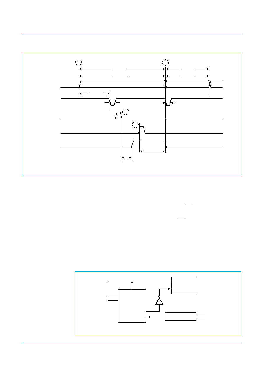
Philips Semiconductors
ISP1161A1
USB single-chip host and device controller
Product data
Rev. 03 -- 23 December 2004
83 of 136
9397 750 13961
© Koninklijke Philips Electronics N.V. 2004. All rights reserved.
In
Figure 38
:
·
A: indicates the point at which the USB bus enters the idle state.
·
B: indicates resume condition, which can be a 20 ms K-state on the USB bus, a
HIGH level on pin D_WAKEUP, or a LOW level on pin CS.
·
C: indicates remote wake-up. The ISP1161A1 will drive a K-state on the USB bus
for 10 ms after pin D_WAKEUP goes HIGH or pin CS goes LOW.
·
D: after detecting the suspend interrupt, set and clear bit GOSUSP in the DcMode
register.
Powered-off application:
Figure 39
shows a typical bus-powered modem
application using the ISP1161A1. The SUSPEND output switches off power to the
microcontroller and other external circuits during the suspend state. The ISP1161A1
DC is woken up through the USB bus (global resume) or by the ring detection circuit
on the telephone line.
Fig 38. Suspend and resume timing.
004aaa359
INT_N
> 5 ms
suspend
interrupt
USB BUS
GOSUSP
WAKEUP
SUSPEND
idle state
10 ms
K-state
> 3 ms
1.8 ms to 2.2 ms
0.5 ms to 3.5 ms
resume
interrupt
A
C
D
B
Fig 39. SUSPEND and WAKEUP signals in a powered-off modem application.
WAKEUP
8031
RST
RING DETECTION
ISP1161A
DP
DM
USB
VBUS
VBUS
VCC
LINE
004aaa674
SUSPEND

Philips Semiconductors
ISP1161A1
USB single-chip host and device controller
Product data
Rev. 03 -- 23 December 2004
84 of 136
9397 750 13961
© Koninklijke Philips Electronics N.V. 2004. All rights reserved.
11.4.2
Resume conditions
A wake-up from the suspend state is initiated either by the USB host or by the
application:
·
USB host: drives a K-state on the USB bus (global resume)
·
Application: remote wake-up through a HIGH level on input WAKEUP or a LOW
level on input CS, if enabled using bit WKUPCS in the DcHardwareConfiguration
register. Wake-up on CS will work only if V
BUS
is present.
The steps of a wake-up sequence are as follows:
1. The internal oscillator and the PLL multiplier are re-enabled. When stabilized, the
clock signals are routed to all internal circuits of the ISP1161A1.
2. The SUSPEND output is deasserted, and bit RESUME in the DcInterrupt register
is set. This will generate an interrupt if bit IERESM in the DcInterruptEnable
register is set.
3. Maximum 15 ms after starting the wake-up sequence, the ISP1161A1 DC
resumes its normal functionality.
4. In case of a remote wake-up, the ISP1161A1 DC drives a K-state on the USB bus
for 10 ms.
5. Following the deassertion of output SUSPEND, the application restores itself and
other system components to the normal operating mode.
6. After wake-up, the internal registers of the ISP1161A1 DC are write-protected to
prevent corruption by inadvertent writing during power-up of external
components. The firmware must send an Unlock Device command to the
ISP1161A1 DC to restore its full functionality.
11.4.3
Control bits in suspend and resume
Table 69:
Summary of control bits
Register
Bit
Function
DcInterrupt
SUSPND
a transition from awake to the suspend state was detected
BUSTATUS
monitors USB bus status (logic 1 = suspend); used when
interrupt is serviced
RESUME
a transition from suspend to the resume state was detected
DcInterrupt
Enable
IESUSP
enables output INT to signal the suspend state
IERESM
enables output INT to signal the resume state
DcMode
SOFTCT
enables SoftConnect pull-up resistor to USB bus
GOSUSP
a HIGH-to-LOW transition enables the suspend state
DcHardware
Configuration
EXTPUL
selects internal (SoftConnect) or external pull-up resistor
WKUPCS
enables wake-up on LOW level of input CS
PWROFF
selects powered-off mode during the suspend state
DcUnlock
all
sending data AA37H unlocks the internal registers for
writing after a resume

Philips Semiconductors
ISP1161A1
USB single-chip host and device controller
Product data
Rev. 03 -- 23 December 2004
85 of 136
9397 750 13961
© Koninklijke Philips Electronics N.V. 2004. All rights reserved.
12. DC DMA transfer
Direct Memory Access (DMA) is a method to transfer data from one location to
another in a computer system, without intervention of the Central Processor Unit
(CPU). Many different implementations of DMA exist. The ISP1161A1 DC supports
two methods:
·
8237 compatible mode: based on the DMA subsystem of the IBM personal
computers (PC, AT and all its successors and clones); this architecture uses the
Intel 8237 DMA controller and has separate address spaces for memory and I/O
·
DACK-only mode: based on the DMA implementation in some embedded RISC
processors, which has a single address space for both memory and I/O.
The ISP1161A1's DC supports DMA transfer for all 14 configurable endpoints (see
Table 66
). Only one endpoint at a time can be selected for DMA transfer. The DMA
operation of the ISP1161A1's DC can be interleaved with normal I/O mode access to
other endpoints.
The following features are supported:
·
Single-cycle or burst transfers (up to 16 bytes per cycle)
·
Programmable transfer direction (read or write)
·
Multiple End-Of-Transfer (EOT) sources: external pin, internal conditions,
short/empty packet
·
Programmable signal levels on pins DREQ2 and EOT.
12.1 Selecting an endpoint for DMA transfer
The target endpoint for DMA access is selected via bits EPDIX[3:0] in the
DcDMAConfiguration register, as shown in
Table 70
. The transfer direction (read or
write) is automatically set by bit EPDIR in the associated ECR, to match the selected
endpoint type (OUT endpoint: read; IN endpoint: write).
Asserting input DACK2 automatically selects the endpoint specified in the
DcDMAConfiguration register, regardless of the current endpoint used for I/O mode
access.
Table 70:
Endpoint selection for DMA transfer
Endpoint
identifier
EPIDX[3:0]
Transfer direction
EPDIR = 0
EPDIR = 1
1
0010
OUT: read
IN: write
2
0011
OUT: read
IN: write
3
0100
OUT: read
IN: write
4
0101
OUT: read
IN: write
5
0110
OUT: read
IN: write
6
0111
OUT: read
IN: write
7
1000
OUT: read
IN: write
8
1001
OUT: read
IN: write
9
1010
OUT: read
IN: write
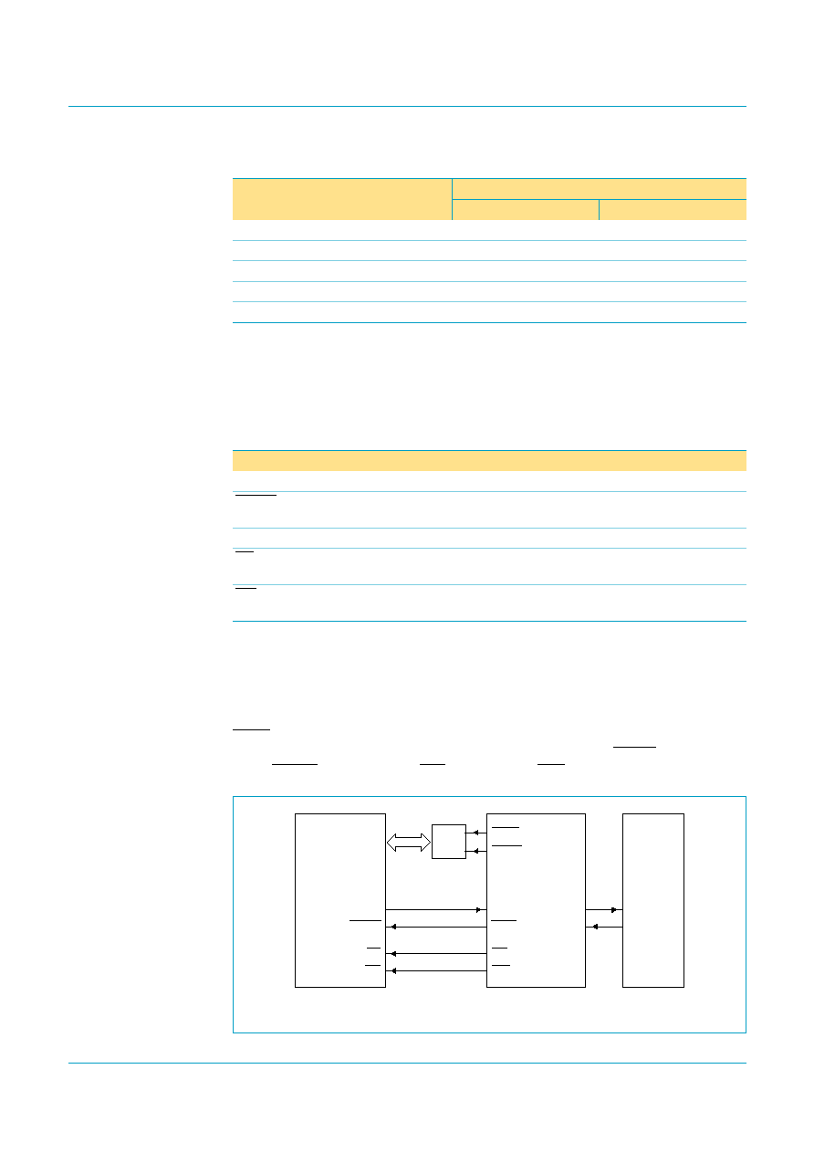
Philips Semiconductors
ISP1161A1
USB single-chip host and device controller
Product data
Rev. 03 -- 23 December 2004
86 of 136
9397 750 13961
© Koninklijke Philips Electronics N.V. 2004. All rights reserved.
12.2 8237 compatible mode
The 8237 compatible DMA mode is selected by clearing bit DAKOLY in the
DcHardwareConfiguration register (see
Table 82
). The pin functions for this mode are
shown in
Table 71
.
The DMA subsystem of an IBM compatible PC is based on the Intel 8237 DMA
controller. It operates as a `fly-by' DMA controller: the data is not stored in the DMA
controller, but it is transferred between an I/O port and a memory address. A typical
example of the ISP1161A1's DC in 8237 compatible DMA mode is given in
Figure 40
.
The 8237 has two control signals for each DMA channel: DREQ (DMA Request) and
DACK (DMA Acknowledge). General control signals are HRQ (Hold Request) and
HLDA (Hold Acknowledge). The bus operation is controlled via MEMR (Memory
read), MEMW (Memory write), IOR (I/O read) and IOW (I/O write).
10
1011
OUT: read
IN: write
11
1100
OUT: read
IN: write
12
1101
OUT: read
IN: write
13
1110
OUT: read
IN: write
14
1111
OUT: read
IN: write
Table 70:
Endpoint selection for DMA transfer
...continued
Endpoint
identifier
EPIDX[3:0]
Transfer direction
EPDIR = 0
EPDIR = 1
Table 71:
8237 compatible mode: pin functions
Symbol
Description
I/O
Function
DREQ2
DC's DMA request
O
ISP1161A1's DC requests a DMA transfer
DACK2
DC's DMA
acknowledge
I
DMA controller confirms the transfer
EOT
end of transfer
I
DMA controller terminates the transfer
RD
read strobe
I
instructs the ISP1161A1's DC to put data
on the bus
WR
write strobe
I
instructs the ISP1161A1's DC to get data
from the bus
Fig 40. ISP1161A1's device controller in 8237 compatible DMA mode.
D0 to D15
CPU
004aaa185
RAM
ISP1161A1
DEVICE
CONTROLLER
DMA
CONTROLLER
8237
DREQ2
DACK2
DREQ
HRQ
HLDA
HRQ
HLDA
DACK
IOR
IOW
MEMR
MEMW
RD
WR

Philips Semiconductors
ISP1161A1
USB single-chip host and device controller
Product data
Rev. 03 -- 23 December 2004
87 of 136
9397 750 13961
© Koninklijke Philips Electronics N.V. 2004. All rights reserved.
The following example shows the steps which occur in a typical DMA transfer:
1. The ISP1161A1's DC receives a data packet in one of its endpoint FIFOs; the
packet must be transferred to memory address 1234H.
2. The ISP1161A1's DC asserts the DREQ2 signal requesting the 8237 for a DMA
transfer.
3. The 8237 asks the CPU to release the bus by asserting the HRQ signal.
4. After completing the current instruction cycle, the CPU places the bus control
signals (MEMR, MEMW, IOR and IOW) and the address lines in three-state and
asserts HLDA to inform the 8237 that it has control of the bus.
5. The 8237 now sets its address lines to 1234H and activates the MEMW and IOR
control signals.
6. The 8237 asserts DACK to inform the ISP1161A1's DC that it will start a DMA
transfer.
7. The ISP1161A1's DC now places the word to be transferred on the data bus
lines, because its RD signal was asserted by the 8237.
8. The 8237 waits one DMA clock period and then de-asserts MEMW and IOR. This
latches and stores the word at the desired memory location. It also informs the
ISP1161A1's DC that the data on the bus lines has been transferred.
9. The ISP1161A1's DC de-asserts the DREQ2 signal to indicate to the 8237 that
DMA is no longer needed. In Single cycle mode this is done after each word, in
Burst mode following the last transferred word of the DMA cycle.
10. The 8237 de-asserts the DACK output indicating that the ISP1161A1's DC must
stop placing data on the bus.
11. The 8237 places the bus control signals (MEMR, MEMW, IOR and IOW) and the
address lines in three-state and de-asserts the HRQ signal, informing the CPU
that it has released the bus.
12. The CPU acknowledges control of the bus by de-asserting HLDA. After activating
the bus control lines (MEMR, MEMW, IOR and IOW) and the address lines, the
CPU resumes the execution of instructions.
For a typical bulk transfer the above process is repeated, once for each byte. After
each byte the address register in the DMA controller is incremented and the byte
counter is decremented. When using 16-bit DMA the number of transfers is 32, and
address incrementing and byte counter decrementing is done by 2 for each word.
12.3 DACK-only mode
The DACK-only DMA mode is selected by setting bit DAKOLY in the
DcHardwareConfiguration register (see
Table 82
). The pin functions for this mode are
shown in
Table 72
. A typical example of the ISP1161A1's DC in DACK-only DMA
mode is given in
Figure 41
.
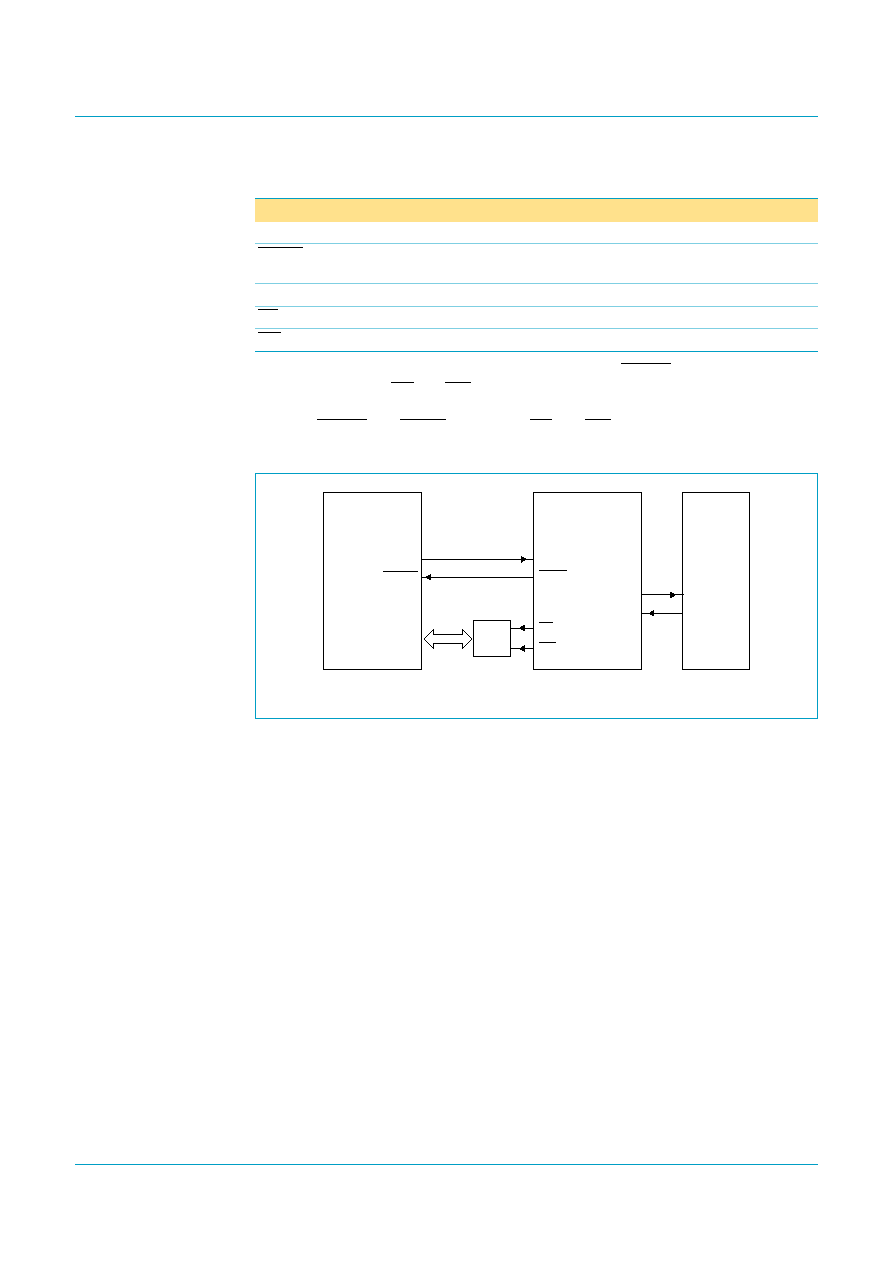
Philips Semiconductors
ISP1161A1
USB single-chip host and device controller
Product data
Rev. 03 -- 23 December 2004
88 of 136
9397 750 13961
© Koninklijke Philips Electronics N.V. 2004. All rights reserved.
In the DACK-only mode, the ISP1161A1's DC uses the DACK2 signal as a data
strobe. Input signals RD and WR are ignored. This mode is used in CPU systems that
have a single address space for memory and I/O access. Such systems have no
separate MEMW and MEMR signals: the RD and WR signals are also used as
memory data strobes.
12.4 End-Of-Transfer conditions
12.4.1
Bulk endpoints
A DMA transfer to/from a bulk endpoint can be terminated by any of the following
conditions (bit names refer to the DcDMAConfiguration register, see
Table 86
):
·
An external End-Of-Transfer signal occurs on input EOT
·
The DMA transfer completes as programmed in the DcDMACounter register
(CNTREN = 1)
·
A short packet is received on an enabled OUT endpoint (SHORTP = 1)
·
DMA operation is disabled by clearing bit DMAEN.
External EOT:
When reading from an OUT endpoint, an external EOT will stop the
DMA operation and clear any remaining data in the current FIFO. For a double-
buffered endpoint the other (inactive) buffer is not affected.
When writing to an IN endpoint, an EOT will stop the DMA operation and the data
packet in the FIFO (even if it is smaller than the maximum packet size) will be sent to
the USB host at the next IN token.
Table 72:
DACK-only mode: pin functions
Symbol
Description
I/O
Function
DREQ2
DC's DMA request
O
ISP1161A1 DC requests a DMA transfer
DACK2
DC's DMA
acknowledge
I
DMA controller confirms the transfer;
also functions as data strobe
EOT
End-Of-Transfer
I
DMA controller terminates the transfer
RD
read strobe
I
not used
WR
write strobe
I
not used
Fig 41. ISP1161A1's device controller in DACK-only DMA mode.
RAM
ISP1161A1
DEVICE
CONTROLLER
DMA
CONTROLLER
CPU
DREQ2
DACK2
HRQ
HLDA
HRQ
HLDA
DREQ
DACK
RD
WR
004aaa186
D0 to D15

Philips Semiconductors
ISP1161A1
USB single-chip host and device controller
Product data
Rev. 03 -- 23 December 2004
89 of 136
9397 750 13961
© Koninklijke Philips Electronics N.V. 2004. All rights reserved.
DcDMACounter register:
An EOT from the DcDMACounter register is enabled by
setting bit CNTREN in the DcDMAConfiguration register. The ISP1161A1 has a 16-bit
DcDMACounter register, which specifies the number of bytes to be transferred. When
DMA is enabled (DMAEN = 1), the internal DMA counter is loaded with the value from
the DcDMACounter register. When the internal counter completes the transfer as
programmed in the DcDMACounter, an EOT condition is generated and the DMA
operation stops.
Short packet:
Normally, the transfer byte count must be set via a control endpoint
before any DMA transfer takes place. When a short packet has been enabled as EOT
indicator (SHORTP = 1), the transfer size is determined by the presence of a short
packet in the data. This mechanism permits the use of a fully autonomous data
transfer protocol.
When reading from an OUT endpoint, reception of a short packet at an OUT token
will stop the DMA operation after transferring the data bytes of this packet.
[1]
The DMA transfer stops. However, no interrupt is generated.
12.4.2
Isochronous endpoints
A DMA transfer to/from an isochronous endpoint can be terminated by any of the
following conditions (bit names refer to the DcDMAConfiguration register, see
Table 86
):
·
An external End-Of-Transfer signal occurs on input EOT
·
The DMA transfer completes as programmed in the DcDMACounter register
(CNTREN = 1)
·
An End-Of-Packet (EOP) signal is detected
·
DMA operation is disabled by clearing bit DMAEN.
Table 73:
Summary of EOT conditions for a bulk endpoint
EOT condition
OUT endpoint
IN endpoint
EOT input
EOT is active
EOT is active
DcDMACounter register
transfer completes as
programmed in the
DcDMACounter register
transfer completes as
programmed in the
DcDMACounter register
Short packet
short packet is received and
transferred
counter reaches zero in the
middle of the buffer
Bit DMAEN in
DcDMAConfiguration register
DMAEN = 0
[1]
DMAEN = 0
[1]
Table 74:
Recommended EOT usage for isochronous endpoints
EOT condition
OUT endpoint
IN endpoint
EOT input active
do not use
preferred
DMA Counter register zero
do not use
preferred
End-Of-Packet
preferred
do not use

Philips Semiconductors
ISP1161A1
USB single-chip host and device controller
Product data
Rev. 03 -- 23 December 2004
90 of 136
9397 750 13961
© Koninklijke Philips Electronics N.V. 2004. All rights reserved.
13. DC commands and registers
The functions and registers of the ISP1161A1's DC are accessed via commands,
which consist of a command code followed by optional data bytes (read or write
action). An overview of the available commands and registers is given in
Table 75
.
A complete access consists of two phases:
1. Command phase: when address bit A0 = 1, the DC interprets the data on the
lower byte of the bus (bits D7 to D0) as a command code. Commands without a
data phase are executed immediately.
2. Data phase (optional): when address bit A0 = 0, the DC transfers the data on
the bus to or from a register or endpoint FIFO. Multi-byte registers are accessed
least significant byte/word first.
As the ISP1161A1 DC's data bus is 16 bits wide:
·
The upper byte (bits D15 to D8) in command phase, or the undefined byte in data
phase and is ignored.
·
The access of registers is word-aligned: byte access is not allowed.
·
If the packet length is odd, the upper byte of the last word in an IN endpoint buffer
is not transmitted to the host. When reading from an OUT endpoint buffer, the
upper byte of the last word must be ignored by the firmware. The packet length is
stored in the first 2 bytes of the endpoint buffer.
Table 75:
DC command and register summary
Name
Destination
Code
(Hex)
Transaction
[1]
Reference
Initialization commands
Write Control OUT
Configuration
DcEndpointConfiguration
register endpoint 0 OUT
20
write 1 word
Section 13.1.1 on page 92
Write Control
IN Configuration
DcEndpointConfiguration
register endpoint 0 IN
21
write 1 word
Write Endpoint
n Configuration (n = 1 to 14)
DcEndpointConfiguration
register endpoint 1 to 14
22 to 2F
write 1 word
Read Control OUT
Configuration
DcEndpointConfiguration
register endpoint 0 OUT
30
read 1 word
Read Control
IN Configuration
DcEndpointConfiguration
register endpoint 0 IN
31
read 1 word
Read Endpoint
n Configuration (n = 1 to 14)
DcEndpointConfiguration
register endpoint 1 to 14
32 to 3F
read 1 word
Write/Read Device Address
DcAddress register
B6/B7
write/read 1 word
Section 13.1.2 on page 93
Write/Read Mode register
DcMode register
B8/B9
write/read 1 word
Section 13.1.3 on page 94
Write/Read Hardware
Configuration
DcHardwareConfiguration
register
BA/BB
write/read 1 word
Section 13.1.4 on page 94
Write/Read
DcInterruptEnable register
DcInterruptEnable register
C2/C3
write/read 2 words
Section 13.1.5 on page 96
Write/Read DMA
Configuration
DcDMAConfiguration
register
F0/F1
write/read 1 word
Section 13.1.6 on page 97

Philips Semiconductors
ISP1161A1
USB single-chip host and device controller
Product data
Rev. 03 -- 23 December 2004
91 of 136
9397 750 13961
© Koninklijke Philips Electronics N.V. 2004. All rights reserved.
Write/Read DMA Counter
DcDMACounter register
F2/F3
write/read 1 word
Section 13.1.7 on page 98
Reset Device
resets all registers
F6
-
Section 13.1.8 on page 99
Data flow commands
Write Control OUT Buffer
illegal: endpoint is read-only
(00)
-
Section 13.2.1 on page 99
Write Control IN Buffer
FIFO endpoint 0 IN
01
N
64 bytes
Write Endpoint n Buffer
(n = 1 to 14)
FIFO endpoint 1 to 14
(IN endpoints only)
02 to 0F
isochronous:
N
1023 bytes
interrupt/bulk:
N
64 bytes
Read Control OUT Buffer
FIFO endpoint 0 OUT
10
N
64 bytes
Read Control IN Buffer
illegal: endpoint is write-only (11)
-
Read Endpoint n Buffer
(n = 1 to 14)
FIFO endpoint 1 to 14
(OUT endpoints only)
12 to 1F
isochronous:
N
1023 bytes
[6]
interrupt/bulk:
N
64 bytes
Stall Control OUT Endpoint
Endpoint 0 OUT
40
-
Stall Control IN Endpoint
Endpoint 0 IN
41
-
Stall Endpoint n
(n = 1 to 14)
Endpoint 1 to 14
42 to 4F
-
Read Control OUT Status
DcEndpointStatus register
endpoint 0 OUT
50
read 1 word
Section 13.2.2 on page 100
Read Control IN Status
DcEndpointStatus register
endpoint 0 IN
51
read 1 word
Read Endpoint n Status
(n = 1 to 14)
DcEndpointStatus register n
endpoint 1 to 14
52 to 5F
read 1 word
Validate Control OUT Buffer
illegal: IN endpoints only
[2]
(60)
-
Section 13.2.4 on page 102
Validate Control IN Buffer
FIFO endpoint 0 IN
[2]
61
none
Validate Endpoint n Buffer
(n = 1 to 14)
FIFO endpoint 1 to 14
(IN endpoints only)
[2]
62 to 6F
none
Clear Control OUT Buffer
FIFO endpoint 0 OUT
70
none
Section 13.2.5 on page 102
Clear Control IN Buffer
illegal
[3]
(71)
-
Clear Endpoint n Buffer
(n = 1 to 14)
FIFO endpoint 1 to 14
(OUT endpoints only)
[3]
72 to 7F
none
Unstall Control OUT
Endpoint
Endpoint 0 OUT
80
-
Section 13.2.3 on page 101
Unstall Control IN Endpoint
Endpoint 0 IN
81
-
Unstall Endpoint n
(n = 1 to 14)
Endpoint 1 to 14
82 to 8F
-
Check Control OUT Status
[4]
DcEndpointStatusImage
register endpoint 0 OUT
D0
read 1 word
Section 13.2.6 on page 102
Check Control IN Status
[4]
DcEndpointStatusImage
register endpoint 0 IN
D1
read 1 word
Check Endpoint n Status
(n = 1 to 14)
[4]
DcEndpointStatusImage
register n endpoint 1 to 14
D2 to DF
read 1 word
Table 75:
DC command and register summary
...continued
Name
Destination
Code
(Hex)
Transaction
[1]
Reference

Philips Semiconductors
ISP1161A1
USB single-chip host and device controller
Product data
Rev. 03 -- 23 December 2004
92 of 136
9397 750 13961
© Koninklijke Philips Electronics N.V. 2004. All rights reserved.
[1]
With N representing the number of bytes, the number of words for 16-bit bus width is: (N + 1)/2.
[2]
Validating an OUT endpoint buffer causes unpredictable behavior of the ISP1161A1's DC.
[3]
Clearing an IN endpoint buffer causes unpredictable behavior of the ISP1161A1's DC.
[4]
Reads a copy of the Status register: executing this command does not clear any status bits or interrupt bits.
[5]
When accessing an 8-bit register in 16-bit mode, the upper byte is invalid.
[6]
During isochronous transfer in 16-bit mode, because N
1023, the firmware must take care of the upper byte.
13.1 Initialization commands
Initialization commands are used during the enumeration process of the USB
network. These commands are used to configure and enable the embedded
endpoints. They also serve to set the USB assigned address of the ISP1161A1's DC
and to perform a device reset.
13.1.1
DcEndpointConfiguration register (R/W: 30H3FH/20H2FH)
This command is used to access the Endpoint Configuration register (ECR) of the
target endpoint. It defines the endpoint type (isochronous or bulk/interrupt), direction
(OUT/IN), FIFO size and buffering scheme. It also enables the endpoint FIFO. The
register bit allocation is shown in
Table 76
. A bus reset will disable all endpoints.
The allocation of FIFO memory only takes place after all 16 endpoints have been
configured in sequence (from endpoint 0 OUT to endpoint 14). Although the control
endpoints have fixed configurations, they must be included in the initialization
sequence and be configured with their default values (see
Table 66
). Automatic FIFO
allocation starts when endpoint 14 has been configured.
Remark: If any change is made to an endpoint configuration which affects the
allocated memory (size, enable/disable), the FIFO memory contents of all endpoints
becomes invalid. Therefore, all valid data must be removed from enabled endpoints
before changing the configuration.
Code (Hex): 20 to 2F -- write (control OUT, control IN, endpoint 1 to 14)
Code (Hex): 30 to 3F -- read (control OUT, control IN, endpoint 1 to 14)
Acknowledge Setup
Endpoint 0 IN and OUT
F4
none
Section 13.2.7 on page 103
General commands
Read Control OUT Error
Code
DcErrorCode register
endpoint 0 OUT
A0
read 1 word
[5]
Section 13.3.1 on page 103
Read Control IN Error Code
DcErrorCode register
endpoint 0 IN
A1
read 1 word
[5]
Read Endpoint n Error Code
(n = 1 to 14)
DcErrorCode register
endpoint 1 to 14
A2 to AF
read 1 word
[5]
Unlock Device
all registers with write
access
B0
write 1 word
Section 13.3.2 on page 104
Write/Read Scratch register
DcScratch register
B2/B3
write/read 1 word
Section 13.3.3 on page 105
Read Frame Number
DcFrameNumber register
B4
read 1 word
Section 13.3.4 on page 105
Read Chip ID
DcChipID register
B5
read 1 word
Section 13.3.5 on page 106
Read Interrupt register
DcInterrupt register
C0
read 2 words
Section 13.3.6 on page 107
Table 75:
DC command and register summary
...continued
Name
Destination
Code
(Hex)
Transaction
[1]
Reference

Philips Semiconductors
ISP1161A1
USB single-chip host and device controller
Product data
Rev. 03 -- 23 December 2004
93 of 136
9397 750 13961
© Koninklijke Philips Electronics N.V. 2004. All rights reserved.
Transaction -- write/read 1 word
13.1.2
DcAddress register (R/W: B7H/B6H)
This command is used to set the USB assigned address in the DcAddress register
and enable the USB device. The DcAddress register bit allocation is shown in
Table 78
.
A USB bus reset sets the device address to 00H (internally) and enables the device.
The value of the DcAddress register (accessible by the microcontroller) is not altered
by the bus reset. In response to the standard USB request, Set Address, the firmware
must issue a Write Device Address command, followed by sending an empty packet
to the host. The new device address is activated when the host acknowledges the
empty packet.
Code (Hex): B6/B7 -- write/read DcAddress register
Transaction -- write/read 1 word
Table 76:
DcEndpointConfiguration register: bit allocation
Bit
7
6
5
4
3
2
1
0
Symbol
FIFOEN
EPDIR
DBLBUF
FFOISO
FFOSZ[3:0]
Reset
0
0
0
0
0
0
0
0
Access
R/W
R/W
R/W
R/W
R/W
R/W
R/W
R/W
Table 77:
DcEndpointConfiguration register: bit description
Bit
Symbol
Description
7
FIFOEN
A logic 1 indicates an enabled FIFO with allocated memory.
A logic 0 indicates a disabled FIFO (no bytes allocated).
6
EPDIR
This bit defines the endpoint direction (0 = OUT, 1 = IN); it also
determines the DMA transfer direction (0 = read, 1 = write).
5
DBLBUF
A logic 1 indicates that this endpoint has double buffering.
4
FFOISO
A logic 1 indicates an isochronous endpoint. A logic 0 indicates
a bulk or interrupt endpoint.
3 to 0
FFOSZ[3:0]
Selects the FIFO size according to
Table 67
Table 78:
DcAddress register: bit allocation
Bit
7
6
5
4
3
2
1
0
Symbol
DEVEN
DEVADR[6:0]
Reset
0
0
0
0
0
0
0
0
Access
R/W
R/W
R/W
R/W
R/W
R/W
R/W
R/W
Table 79:
DcAddress register: bit description
Bit
Symbol
Description
7
DEVEN
A logic 1 enables the device.
6 to 0
DEVADR[6:0]
This field specifies the USB device address.

Philips Semiconductors
ISP1161A1
USB single-chip host and device controller
Product data
Rev. 03 -- 23 December 2004
94 of 136
9397 750 13961
© Koninklijke Philips Electronics N.V. 2004. All rights reserved.
13.1.3
DcMode register (R/W: B9H/B8H)
This command is used to access the ISP1161A1's DcMode register, which consists
of 1 byte (for bit allocation: see
Table 79
). In 16-bit bus mode the upper byte is
ignored.
The DcMode register controls the DMA bus width, resume and suspend modes,
interrupt activity and SoftConnect operation. It can be used to enable debug mode,
where all errors and Not Acknowledge (NAK) conditions will generate an interrupt.
Code (Hex): B8/B9 -- write/read Mode register
Transaction -- write/read 1 word
[1]
Unchanged by a bus reset.
13.1.4
DcHardwareConfiguration register (R/W: BBH/BAH)
This command is used to access the DcHardwareConfiguration register, which
consists of 2 bytes. The first (lower) byte contains the device configuration and
control values, the second (upper) byte holds the clock control bits and the clock
division factor. The bit allocation is given in
Table 82
. A bus reset will not change any
of the programmed bit values.
Table 80:
DcMode register: bit allocation
Bit
7
6
5
4
3
2
1
0
Symbol
DMAWD
reserved
GOSUSP
reserved
INTENA
DBGMOD
reserved
SOFTCT
Reset
0
[1]
0
0
0
0
[1]
0
[1]
0
[1]
0
[1]
Access
R/W
R/W
R/W
R/W
R/W
R/W
R/W
R/W
Table 81:
DcMode register: bit description
Bit
Symbol
Description
7
DMAWD
A logic 1 selects 16-bit DMA bus width (bus configuration
modes 0 and 2). A logic 0 selects 8-bit DMA bus width. Bus
reset value: unchanged.
6
-
reserved
5
GOSUSP
Writing a logic 1 followed by a logic 0 will activate `suspend'
mode.
4
-
reserved
3
INTENA
A logic 1 enables all DC interrupts. Bus reset value: unchanged;
for details, see
Section 8.6.3
.
2
DBGMOD
A logic 1 enables debug mode where all NAKs and errors will
generate an interrupt. A logic 0 selects normal operation, where
interrupts are generated on every ACK (bulk endpoints) or after
every data transfer (isochronous endpoints).
Bus reset value: unchanged.
1
-
reserved
0
SOFTCT
A logic 1 enables SoftConnect (see
Section 7.5
). This bit is
ignored if EXTPUL = 1 in the DcHardwareConfiguration register
(see
Table 82
). Bus reset value: unchanged.

Philips Semiconductors
ISP1161A1
USB single-chip host and device controller
Product data
Rev. 03 -- 23 December 2004
95 of 136
9397 750 13961
© Koninklijke Philips Electronics N.V. 2004. All rights reserved.
The DcHardwareConfiguration register controls the connection to the USB bus, clock
activity and power supply during `suspend' state, output clock frequency, DMA
operating mode and pin configurations (polarity, signalling mode).
Code (Hex): BA/BB -- write/read DcHardwareConfiguration register
Transaction -- write/read 1 word
Table 82:
DcHardwareConfiguration register: bit allocation
Bit
15
14
13
12
11
10
9
8
Symbol
reserved
EXTPUL
NOLAZY
CLKRUN
CLKDIV[3:0]
Reset
0
0
1
0
0
0
1
1
Access
R/W
R/W
R/W
R/W
R/W
R/W
R/W
R/W
Bit
7
6
5
4
3
2
1
0
Symbol
DAKOLY
DRQPOL
DAKPOL
EOTPOL
WKUPCS
PWROFF
INTLVL
INTPOL
Reset
0
1
0
0
0
0
0
0
Access
R/W
R/W
R/W
R/W
R/W
R/W
R/W
R/W
Table 83:
DcHardwareConfiguration register: bit description
Bit
Symbol
Description
15
-
reserved
14
EXTPUL
A logic 1 indicates that an external 1.5 k
pull-up resistor is
used on pin D
+
and that SoftConnect is not used. Bus reset
value: unchanged.
13
NOLAZY
A logic 1 disables output on pin CLKOUT of the LazyClock
frequency (100 kHz
±
50 %) during `suspend' state. A logic 0
causes pin CLKOUT to switch to LazyClock output after
approximately 2 ms delay, following the setting of bit GOSUSP
in the DcMode register. Bus reset value: unchanged.
12
CLKRUN
A logic 1 indicates that the internal clocks are always running,
even during `suspend' state. A logic 0 switches off the internal
oscillator and PLL, when they are not needed. During `suspend'
state this bit must be made logic 0 to meet the suspend current
requirements. The clock is stopped after a delay of
approximately 2 ms, following the setting of bit GOSUSP in the
DcMode register. Bus reset value: unchanged.
11 to 8
CLKDIV[3:0]
This field specifies the clock division factor N, which controls the
clock frequency on output CLKOUT. The output frequency in
MHz is given by 48 / (N + 1). The clock frequency range is
3 MHz to 48 MHz (N = 0 to 15) with a reset value of 12 MHz
(N = 3). The hardware design guarantees no glitches during
frequency change. Bus reset value: unchanged.
7
DAKOLY
A logic 1 selects DACK-only DMA mode. A logic 0 selects
8237 compatible DMA mode. Bus reset value: unchanged.
6
DRQPOL
Selects DREQ2 pin signal polarity (0 = active LOW, 1 = active
HIGH). Bus reset value: unchanged.
5
DAKPOL
Selects DACK2 pin signal polarity (0 = active LOW).
Bus reset value: unchanged.
4
EOTPOL
Selects EOT pin signal polarity (0 = active LOW, 1 = active
HIGH). Bus reset value: unchanged.
Philips Semiconductors
ISP1161A1
USB single-chip host and device controller
Product data
Rev. 03 -- 23 December 2004
96 of 136
9397 750 13961
© Koninklijke Philips Electronics N.V. 2004. All rights reserved.
13.1.5
DcInterruptEnable register (R/W: C3H/C2H)
This command is used to individually enable or disable interrupts from all endpoints,
as well as interrupts caused by events on the USB bus (SOF, SOF lost, EOT,
suspend, resume, reset). That is, if an interrupt event occurs while the interrupt is not
enabled, nothing will be seen on the interrupt pin. Even if you then enable the
interrupt during the interrupt event, there will still be no interrupt seen on the interrupt
pin, see
Figure 42
.
The DcInterrupt register will not register any interrupt, if it is not already enabled
using the DcInterruptEnable register. The DcInterruptEnable register is not an
Interrupt Mask register.
A bus reset will not change any of the programmed bit values.
The command accesses the DcInterruptEnable register, which consists of 4 bytes.
The bit allocation is given in
Table 84
.
Remark: For details on interrupt control, see
Section 8.6.3
.
3
WKUPCS
A logic 1 enables remote wake-up via a LOW level on input
pin CS (V
BUS
must be present for wake-up on CS).
Bus reset value: unchanged.
2
PWROFF
A logic 1 enables powering-off during `suspend' state. Output
D_SUSPEND pin is configured as a power switch control signal
for external devices (HIGH during `suspend'). This value should
always be initialized to logic 1. Bus reset value: unchanged.
1
INTLVL
Selects the interrupt signalling mode on output pin INT2
(0 = level, 1 = pulsed). In pulsed mode an interrupt produces an
166 ns pulse. See
Section 8.6.3
for details.
Bus reset value: unchanged.
0
INTPOL
Selects INT2 pin signal polarity (0 = active LOW, 1 = active
HIGH). Bus reset value: unchanged.
Table 83:
DcHardwareConfiguration register: bit description
...continued
Bit
Symbol
Description
Pin INT2: HIGH = de-assert; LOW = assert; INTENA = 1.
Fig 42. Interrupt pin waveform.
INT2 pin
interrupt
event
occurs
interrupt
event
occurs
DcInterruptEnable
register
disabled
DcInterruptEnable
register
enabled
interrupt is cleared
004aaa197

Philips Semiconductors
ISP1161A1
USB single-chip host and device controller
Product data
Rev. 03 -- 23 December 2004
97 of 136
9397 750 13961
© Koninklijke Philips Electronics N.V. 2004. All rights reserved.
Code (Hex): C2/C3 -- write/read DcInterruptEnable register
Transaction -- write/read 2 words
13.1.6
DcDMAConfiguration register (R/W: F1H/F0H)
This command defines the DMA configuration of the ISP1161A1's DC and
enables/disables DMA transfers. The command accesses the DcDMAConfiguration
register, which consists of 2 bytes. The bit allocation is given in
Table 86
. A bus reset
will clear bit DMAEN (DMA disabled), all other bits remain unchanged.
Code (Hex): F0/F1 -- write/read DMA Configuration
Transaction -- write/read 1 word
Table 84:
DcInterruptEnable register: bit allocation
Bit
31
30
29
28
27
26
25
24
Symbol
reserved
Reset
00H
Access
R/W
Bit
23
22
21
20
19
18
17
16
Symbol
IEP14
IEP13
IEP12
IEP11
IEP10
IEP9
IEP8
IEP7
Reset
0
0
0
0
0
0
0
0
Access
R/W
R/W
R/W
R/W
R/W
R/W
R/W
R/W
Bit
15
14
13
12
11
10
9
8
Symbol
IEP6
IEP5
IEP4
IEP3
IEP2
IEP1
IEP0IN
IEP0OUT
Reset
0
0
0
0
0
0
0
0
Access
R/W
R/W
R/W
R/W
R/W
R/W
R/W
R/W
Bit
7
6
5
4
3
2
1
0
Symbol
reserved
SP_IEEOT
IEPSOF
IESOF
IEEOT
IESUSP
IERESM
IERST
Reset
0
0
0
0
0
0
0
0
Access
R/W
R/W
R/W
R/W
R/W
R/W
R/W
R/W
Table 85:
DcInterruptEnable register: bit description
Bit
Symbol
Description
31 to 24
-
reserved; must write logic 0
23 to 10
IEP14 to IEP1
A logic 1 enables interrupts from the indicated endpoint.
9
IEP0IN
A logic 1 enables interrupts from the control IN endpoint.
8
IEP0OUT
A logic 1 enables interrupts from the control OUT endpoint.
7
-
reserved
6
SP_IEEOT
A logic 1 enables interrupt upon detection of a short packet.
5
IEPSOF
A logic 1 enables 1 ms interrupts upon detection of
Pseudo SOF.
4
IESOF
A logic 1 enables interrupt upon SOF detection.
3
IEEOT
A logic 1 enables interrupt upon EOT detection.
2
IESUSP
A logic 1 enables interrupt upon detection of `suspend' state.
1
IERESM
A logic 1 enables interrupt upon detection of a `resume' state.
0
IERST
A logic 1 enables interrupt upon detection of a bus reset.

Philips Semiconductors
ISP1161A1
USB single-chip host and device controller
Product data
Rev. 03 -- 23 December 2004
98 of 136
9397 750 13961
© Koninklijke Philips Electronics N.V. 2004. All rights reserved.
[1]
Unchanged by a bus reset.
For selecting an endpoint for device DMA transfer, see
Section 11.2
.
13.1.7
DcDMACounter register (R/W: F3H/F2H)
This command accesses the DcDMACounter register. The bit allocation is given in
Table 88
. Writing to the register sets the number of bytes for a DMA transfer. Reading
the register returns the number of remaining bytes in the current transfer. A bus reset
will not change the programmed bit values.
Table 86:
DcDMAConfiguration register: bit allocation
Bit
15
14
13
12
11
10
9
8
Symbol
CNTREN
SHORTP
reserved
reserved
reserved
reserved
reserved
ODD_
EVEN_IND
Reset
0
[1]
0
[1]
0
[1]
0
[1]
0
[1]
0
[1]
0
[1]
0
Access
R/W
R/W
R/W
R/W
R/W
R/W
R/W
R
Bit
7
6
5
4
3
2
1
0
Symbol
EPDIX[3:0]
DMAEN
reserved
BURSTL[1:0]
Reset
0
[1]
0
[1]
0
[1]
0
[1]
0
0
0
[1]
0
[1]
Access
R/W
R/W
R/W
R/W
R/W
R/W
R/W
R/W
Table 87:
DcDMAConfiguration register: bit description
Bit
Symbol
Description
15
CNTREN
A logic 1 enables the generation of an EOT condition, when the
DMA Counter register reaches zero. Bus reset value:
unchanged.
14
SHORTP
A logic 1 enables short/empty packet mode. When receiving
(OUT endpoint) a short/empty packet an EOT condition is
generated. When transmitting (IN endpoint), this bit should be
cleared. Bus reset value: unchanged.
13 to 9
-
reserved
8
ODD_EVEN_
IND
This bit is logic 0 when the last DMA access is a byte (LSB byte
valid; MSB byte invalid). This bit is logic 1 when the last DMA
access is a word (LSB byte valid; MSB byte invalid).
7 to 4
EPDIX[3:0]
Indicates the destination endpoint for DMA, see
Table 70
.
3
DMAEN
Writing a logic 1 enables DMA transfer, a logic 0 forces the end
of an ongoing DMA transfer. Reading this bit indicates whether
DMA is enabled (0 = DMA stopped, 1 = DMA enabled). This bit
is cleared by a bus reset.
2
-
reserved
1 to 0
BURSTL[1:0]
Selects the DMA burst length:
00 -- single-cycle mode (1 byte)
01 -- burst mode (4 bytes)
10 -- burst mode (8 bytes)
11 -- burst mode (16 bytes).
Bus reset value: unchanged.

Philips Semiconductors
ISP1161A1
USB single-chip host and device controller
Product data
Rev. 03 -- 23 December 2004
99 of 136
9397 750 13961
© Koninklijke Philips Electronics N.V. 2004. All rights reserved.
The internal DMA counter is automatically reloaded from the DcDMACounter register
when DMA is re-enabled (DMAEN = 1). See
Section 13.1.6
for more details.
Code (Hex): F2/F3 -- write/read DcDMACounter register
Transaction -- write/read 1 word
13.1.8
Reset Device (F6H)
This command resets the ISP1161A1 DC in the same way as an external hardware
reset via input RESET. All registers are initialized to their `reset' values.
Code (Hex): F6 -- reset the device
Transaction -- none
13.2 Data flow commands
Data flow commands are used to manage the data transmission between the USB
endpoints and the system microprocessor. Much of the data flow is initiated via an
interrupt to the microprocessor. The data flow commands are used to access the
endpoints and determine whether the endpoint FIFOs contain valid data.
Remark: The IN buffer of an endpoint contains input data for the host, the OUT
buffer receives output data from the host.
13.2.1
Write/Read Endpoint Buffer (R/W: 10H,12H-1FH/01H0FH)
This command is used to access endpoint FIFO buffers for reading or writing. First,
the buffer pointer is reset to the beginning of the buffer. Following the command, a
maximum of (M + 1) words can be written or read, with M given by (N
+
1)/2,
N representing the size of the endpoint buffer. After each read/write action the buffer
pointer is automatically incremented by 2.
In DMA access, the first word (the packet length) is skipped: transfers start at the
second word of the endpoint buffer. When reading, the ISP1161A1 DC can detect the
last word via the End of Packet (EOP) condition. When writing to a bulk/interrupt
endpoint, the endpoint buffer must be completely filled before sending the data to the
host. Exception: when a DMA transfer is stopped by an external EOT condition, the
current buffer content (full or not) is sent to the host.
Table 88:
DcDMACounter register: bit allocation
Bit
15
14
13
12
11
10
9
8
Symbol
DMACR[15:8]
Reset
00H
Access
R/W
Bit
7
6
5
4
3
2
1
0
Symbol
DMACR[7:0]
Reset
00H
Access
R/W
Table 89:
DcDMACounter register: bit description
Bit
Symbol
Description
15 to 0
DMACR[15:0]
DMA Counter register

Philips Semiconductors
ISP1161A1
USB single-chip host and device controller
Product data
Rev. 03 -- 23 December 2004
100 of 136
9397 750 13961
© Koninklijke Philips Electronics N.V. 2004. All rights reserved.
Remark: Reading data after a Write Endpoint Buffer command or writing data after a
Read Endpoint Buffer command will cause unpredictable behavior of the
ISP1161A1 DC.
Code (Hex): 01 to 0F -- write (control IN, endpoint 1 to 14)
Code (Hex): 10, 12 to 1F -- read (control OUT, endpoint 1 to 14)
Transaction -- write/read maximum (M + 1) words (isochronous endpoint: N
1023,
bulk/interrupt endpoint: N
32)
The data in the endpoint FIFO must be organized as shown in
Table 90
. An example
of endpoint FIFO access is given
Table 91
.
Remark: There is no protection against writing or reading past a buffer's boundary or
against writing into an OUT buffer or reading from an IN buffer. Any of these actions
could cause an incorrect operation. Data residing in an OUT buffer are only
meaningful after a successful transaction. Exception: during DMA access of a
double-buffered endpoint, the buffer pointer automatically points to the secondary
buffer after reaching the end of the primary buffer.
13.2.2
DcEndpointStatus register (R: 50H5FH)
This command is used to read the status of an endpoint FIFO. The command
accesses the DcEndpointStatus register, the bit allocation of which is shown in
Table 92
. Reading the DcEndpointStatus register will clear the interrupt bit set for the
corresponding endpoint in the DcInterrupt register (see
Table 108
).
All bits of the DcEndpointStatus register are read-only. Bit EPSTAL is controlled by
the Stall/Unstall commands and by the reception of a SETUP token (see
Section 13.2.3
).
Code (Hex): 50 to 5F -- read (control OUT, control IN, endpoint 1 to 14)
Transaction -- read 1 word
Table 90:
Endpoint FIFO organization
Word #
Description
0 (lower byte)
packet length (lower byte)
0 (upper byte)
packet length (upper byte)
1 (lower byte)
data byte 1
1 (upper byte)
data byte 2
:
:
M = (N + 1)/2
data byte N
Table 91:
Example of endpoint FIFO access
A0
Phase
Bus lines
Word #
Description
1
command
D[7:0]
-
command code (00H to 1FH)
D[15:8]
-
ignored
0
data
D[15:0]
0
packet length
0
data
D[15:0]
1
data word 1 (data byte 2, data byte 1)
0
data
D[15:0]
2
data word 2 (data byte 4, data byte 3)
:
:
:
:
:

Philips Semiconductors
ISP1161A1
USB single-chip host and device controller
Product data
Rev. 03 -- 23 December 2004
101 of 136
9397 750 13961
© Koninklijke Philips Electronics N.V. 2004. All rights reserved.
13.2.3
Stall Endpoint/Unstall Endpoint (40H4FH/80H--8FH)
These commands are used to stall or unstall an endpoint. The commands modify the
content of the DcEndpointStatus register (see
Table 92
).
A stalled control endpoint is automatically unstalled when it receives a SETUP token,
regardless of the packet content. If the endpoint should stay in its stalled state, the
microprocessor can re-stall it with the Stall Endpoint command.
When a stalled endpoint is unstalled (either by the Unstall Endpoint command or by
receiving a SETUP token), it is also re-initialized. This flushes the buffer: if it is an
OUT buffer it waits for a DATA 0 PID, if it is an IN buffer it writes a DATA 0 PID.
Code (Hex): 40 to 4F -- stall (control OUT, control IN, endpoint 1 to 14)
Code (Hex): 80 to 8F -- unstall (control OUT, control IN, endpoint 1 to 14)
Transaction -- none
Table 92:
DcEndpointStatus register: bit allocation
Bit
7
6
5
4
3
2
1
0
Symbol
EPSTAL
EPFULL1
EPFULL0
DATA_PID
OVER
WRITE
SETUPT
CPUBUF
reserved
Reset
0
0
0
0
0
0
0
0
Access
R
R
R
R
R
R
R
R
Table 93:
DcEndpointStatus register: bit description
Bit
Symbol
Description
7
EPSTAL
This bit indicates whether the endpoint is stalled or not
(1 = stalled, 0 = not stalled).
Set to logic 1 by a Stall Endpoint command and cleared to
logic 0 by an Unstall Endpoint command. The endpoint is
automatically unstalled upon reception of a SETUP token.
6
EPFULL1
A logic 1 indicates that the secondary endpoint buffer is full.
5
EPFULL0
A logic 1 indicates that the primary endpoint buffer is full.
4
DATA_PID
This bit indicates the data PID of the next packet (0 = DATA PID,
1 = DATA1 PID).
3
OVERWRITE
This bit is set by hardware, a logic 1 indicating that a new Setup
packet has overwritten the previous set-up information, before it
was acknowledged or before the endpoint was stalled. If writing
the set-up data has finished, this bit is cleared by a read action.
Firmware must check this bit before sending an Acknowledge
Setup command or stalling the endpoint. Upon reading a logic 1,
the firmware must stop ongoing set-up actions and wait for a
new Setup packet.
2
SETUPT
A logic 1 indicates that the buffer contains a Setup packet.
1
CPUBUF
This bit indicates which buffer is currently selected for CPU
access (0 = primary buffer, 1 = secondary buffer).
0
-
reserved

Philips Semiconductors
ISP1161A1
USB single-chip host and device controller
Product data
Rev. 03 -- 23 December 2004
102 of 136
9397 750 13961
© Koninklijke Philips Electronics N.V. 2004. All rights reserved.
13.2.4
Validate Endpoint Buffer (R/W: 6FH/61H)
This command signals the presence of valid data for transmission to the USB host, by
setting the Buffer Full flag of the selected IN endpoint. This indicates that the data in
the buffer is valid and can be sent to the host, when the next IN token is received. For
a double-buffered endpoint this command switches the current FIFO for CPU access.
Remark: For special aspects of the control IN endpoint see
Section 11.3.6
.
Code (Hex): 61 to 6F -- validate endpoint buffer (control IN, endpoint 1 to 14)
Transaction -- none
13.2.5
Clear Endpoint Buffer (70H, 72H7FH)
This command unlocks and clears the buffer of the selected OUT endpoint, allowing
the reception of new packets. Reception of a complete packet causes the Buffer Full
flag of an OUT endpoint to be set. Any subsequent packets are refused by returning a
NAK condition, until the buffer is unlocked using this command. For a double-buffered
endpoint this command switches the current FIFO for CPU access.
Remark: For special aspects of the control OUT endpoint see
Section 11.3.6
.
Code (Hex): 70, 72 to 7F -- clear endpoint buffer (control OUT, endpoint 1 to 14)
Transaction -- none
13.2.6
DcEndpointStatusImage register(D0HDFH)
This command is used to check the status of the selected endpoint FIFO without
clearing any status or interrupt bits. The command accesses the
DcEndpointStatusImage register, which contains a copy of the DcEndpointStatus
register. The bit allocation of the DcEndpointStatusImage register is shown in
Table 94
.
Code (Hex): D0 to DF -- check status (control OUT, control IN, endpoint 1 to 14)
Transaction -- write/read 1 word
Table 94:
DcEndpointStatusImage register: bit allocation
Bit
7
6
5
4
3
2
1
0
Symbol
EPSTAL
EPFULL1
EPFULL0
DATA_PID
OVER
WRITE
SETUPT
CPUBUF
reserved
Reset
0
0
0
0
0
0
0
0
Access
R
R
R
R
R
R
R
R
Table 95:
DcEndpointStatusImage register: bit description
Bit
Symbol
Description
7
EPSTAL
This bit indicates whether the endpoint is stalled or not
(1 = stalled, 0 = not stalled).
6
EPFULL1
A logic 1 indicates that the secondary endpoint buffer is full.
5
EPFULL0
A logic 1 indicates that the primary endpoint buffer is full.
4
DATA_PID
This bit indicates the data PID of the next packet (0 = DATA PID,
1 = DATA1 PID).

Philips Semiconductors
ISP1161A1
USB single-chip host and device controller
Product data
Rev. 03 -- 23 December 2004
103 of 136
9397 750 13961
© Koninklijke Philips Electronics N.V. 2004. All rights reserved.
13.2.7
Acknowledge Setup (F4H)
This command acknowledges to the host that a Setup packet was received. The
arrival of a Setup packet disables the Validate Buffer and Clear Buffer commands for
the control IN and OUT endpoints. The microprocessor needs to re-enable these
commands by sending an Acknowledge Setup command, see
Section 11.3.6
.
Code (Hex): F4 -- acknowledge set-up
Transaction -- none
13.3 General commands
13.3.1
Read Endpoint Error Code (R: A0HAFH)
This command returns the status of the last transaction of the selected endpoint, as
stored in the DcErrorCode register. Each new transaction overwrites the previous
status information. The bit allocation of the DcErrorCode register is shown in
Table 96
.
Code (Hex): A0 to AF -- read error code (control OUT, control IN, endpoint 1 to 14)
Transaction -- read 1 word
3
OVERWRITE
This bit is set by hardware, a logic 1 indicating that a new Setup
packet has overwritten the previous set-up information, before it
was acknowledged or before the endpoint was stalled. If writing
the set-up data has finished, this bit is cleared by a read action.
Firmware must check this bit before sending an Acknowledge
Setup command or stalling the endpoint. Upon reading a logic 1
the firmware must stop ongoing set-up actions and wait for a
new Setup packet.
2
SETUPT
A logic 1 indicates that the buffer contains a Setup packet.
1
CPUBUF
This bit indicates which buffer is currently selected for CPU
access (0 = primary buffer, 1 = secondary buffer).
0
-
reserved
Table 95:
DcEndpointStatusImage register: bit description
...continued
Bit
Symbol
Description
Table 96:
DcErrorCode register: bit allocation
Bit
7
6
5
4
3
2
1
0
Symbol
UNREAD
DATA01
reserved
ERROR[3:0]
RTOK
Reset
0
0
0
0
0
0
0
0
Access
R
R
R
R
R
R
R
R
Table 97:
DcErrorCode register: bit description
Bit
Symbol
Description
7
UNREAD
A logic 1 indicates that a new event occurred before the
previous status was read.
6
DATA01
This bit indicates the PID type of the last successfully received
or transmitted packet (0 = DATA0 PID, 1 = DATA1 PID).

Philips Semiconductors
ISP1161A1
USB single-chip host and device controller
Product data
Rev. 03 -- 23 December 2004
104 of 136
9397 750 13961
© Koninklijke Philips Electronics N.V. 2004. All rights reserved.
13.3.2
Unlock Device (B0H)
This command unlocks the ISP1161A1's DC from write-protection mode after a
`resume'. In `suspend' state all registers and FIFOs are write-protected to prevent
data corruption by external devices during a `resume'. Also, the register access for
reading is possible only after the `Unlock Device' command is executed.
After waking up from `suspend' state, the firmware must unlock the registers and
FIFOs via this command, by writing the unlock code (AA37H) into the Lock register.
The bit allocation of the Lock register is given in
Table 99
.
Code (Hex): B0 -- unlock the device
Transaction -- write 1 word (unlock code)
5
-
reserved
4 to 1
ERROR[3:0]
Error code. For error description, see
Table 98
.
0
RTOK
A logic 1 indicates that data was received or transmitted
successfully.
Table 98:
Transaction error codes
Error code
(Binary)
Description
0000
no error
0001
PID encoding error; bits 7 to 4 are not the inverse of bits 3 to 0
0010
PID unknown; encoding is valid, but PID does not exist
0011
unexpected packet; packet is not of the expected type (token, data, or
acknowledge), or is a token to a non-control endpoint
0100
token CRC error
0101
data CRC error
0110
time-out error
0111
babble error
1000
unexpected end-of-packet
1001
sent or received NAK (Not AcKnowledge)
1010
sent Stall; a token was received, but the endpoint was stalled
1011
overflow; the received packet was larger than the available buffer space
1100
sent empty packet (ISO only)
1101
bit stuffing error
1110
sync error
1111
wrong (unexpected) toggle bit in DATA PID; data was ignored
Table 97:
DcErrorCode register: bit description
...continued
Bit
Symbol
Description
Table 99:
Lock register: bit allocation
Bit
15
14
13
12
11
10
9
8
Symbol
UNLOCKH[7:0]
Reset
AAH
Access
W

Philips Semiconductors
ISP1161A1
USB single-chip host and device controller
Product data
Rev. 03 -- 23 December 2004
105 of 136
9397 750 13961
© Koninklijke Philips Electronics N.V. 2004. All rights reserved.
13.3.3
DcScratch register (R/W: B3H/B2H)
This command accesses the 16-bit DcScratch register, which can be used by the
firmware to save and restore information, e.g., the device status before powering
down in `suspend' state. The register bit allocation is given in
Table 101
.
Code (Hex): B2/B3 -- write/read Scratch register
Transaction -- write/read 1 word
13.3.4
Read Frame Number (R: B4H)
This command returns the frame number of the last successfully received SOF. It is
followed by reading one word from the DcFrameNumber register, containing the
frame number. The DcFrameNumber register is shown in
Table 103
.
Remark: After a bus reset, the value of the DcFrameNumber register is undefined.
Code (Hex): B4 -- read frame number
Transaction -- read 1 word
Bit
7
6
5
4
3
2
1
0
Symbol
UNLOCKL[7:0]
Reset
37H
Access
W
Table 100: Lock register: bit description
Bit
Symbol
Description
15 to 0
UNLOCK[15:0]
Sending data AA37H unlocks the internal registers and FIFOs
for writing, following a `resume'.
Table 101: DcScratch register: bit allocation
Bit
15
14
13
12
11
10
9
8
Symbol
reserved
SFIRH[4:0]
Reset
0
0
0
0
0
0
0
0
Access
R/W
R/W
R/W
R/W
R/W
R/W
R/W
R/W
Bit
7
6
5
4
3
2
1
0
Symbol
SFIRL[7:0]
Reset
00H
Access
R/W
Table 102: DcScratch register: bit description
Bit
Symbol
Description
15 to 13
-
reserved; must be logic 0
12 to 0
SFIR[12:0]
Scratch Information register

Philips Semiconductors
ISP1161A1
USB single-chip host and device controller
Product data
Rev. 03 -- 23 December 2004
106 of 136
9397 750 13961
© Koninklijke Philips Electronics N.V. 2004. All rights reserved.
[1]
Reset value undefined after a bus reset.
13.3.5
Read Chip ID (R: B5H)
This command reads the chip identification code and hardware version number. The
firmware must check this information to determine the supported functions and
features. This command accesses the DcChipID register, which is shown in
Table 106
.
Code (Hex): B5 -- read chip ID
Transaction -- read 1 word
Table 103: DcFrameNumber register: bit allocation
Bit
15
14
13
12
11
10
9
8
Symbol
reserved
SOFRH[2:0]
Reset
[1]
0
0
0
0
0
0
0
0
Access
R
R
R
R
R
R
R
R
Bit
7
6
5
4
3
2
1
0
Symbol
SOFRL[7:0]
Reset
[1]
0
0
0
0
0
0
0
0
Access
R
R
R
R
R
R
R
R
Table 104: DcFrameNumber register: bits description
Bit
Symbol
Description
15 to 11
-
reserved
10 to 8
SOFRH[2:0] SOF frame number (upper byte)
7 to 0
SOFRL[7:0]
SOF frame number (lower byte)
Table 105: Example of DcFrameNumber register access
A0
Phase
Bus lines
Word #
Description
1
command
D[7:0]
-
command code (B4H)
D[15:8]
-
ignored
0
data
D[15:0]
0
frame number
Table 106: DcChipID register: bit allocation
Bit
15
14
13
12
11
10
9
8
Symbol
CHIPIDH[7:0]
Reset
61H
Access
R
Bit
7
6
5
4
3
2
1
0
Symbol
CHIPIDL[7:0]
Reset
23H
Access
R

Philips Semiconductors
ISP1161A1
USB single-chip host and device controller
Product data
Rev. 03 -- 23 December 2004
107 of 136
9397 750 13961
© Koninklijke Philips Electronics N.V. 2004. All rights reserved.
13.3.6
Read Interrupt register (R: C0H)
This command indicates the sources of interrupts as stored in the 4-byte DcInterrupt
register. Each individual endpoint has its own interrupt bit. The bit allocation of the
DcInterrupt register is shown in
Table 108
. Bit BUSTATUS is used to verify the current
bus status in the interrupt service routine. Interrupts are enabled via the
DcInterruptEnable register, see
Section 13.1.5
.
Remark: While reading the DcInterrupt register, read both 2 bytes.
Code (Hex): C0 -- read interrupt register
Transaction -- read 2 words
Remark: For details on interrupt control, see
Section 8.6.3
.
Table 107: DcChipID register: bit description
Bit
Symbol
Description
15 to 8
CHIPIDH[7:0]
chip ID code (61H)
7 to 0
CHIPIDL[7:0]
silicon version (23H, with 23 representing the BCD encoded
version number)
Table 108: DcInterrupt register: bit allocation
Bit
31
30
29
28
27
26
25
24
Symbol
reserved
Reset
00H
Access
R
Bit
23
22
21
20
19
18
17
16
Symbol
EP14
EP13
EP12
EP11
EP10
EP9
EP8
EP7
Reset
0
0
0
0
0
0
0
0
Access
R
R
R
R
R
R
R
R
Bit
15
14
13
12
11
10
9
8
Symbol
EP6
EP5
EP4
EP3
EP2
EP1
EP0IN
EP0OUT
Reset
0
0
0
0
0
0
0
0
Access
R
R
R
R
R
R
R
R
Bit
7
6
5
4
3
2
1
0
Symbol
BUSTATUS
SP_EOT
PSOF
SOF
EOT
SUSPND
RESUME
RESET
Reset
0
0
0
0
0
0
0
0
Access
R
R
R
R
R
R
R
R
Table 109: DcInterrupt register: bit description
Bit
Symbol
Description
31 to 24
-
reserved
23 to 10
EP14 to EP1
A logic 1 indicates the interrupt source(s): endpoint 14 to 1.
9
EP0IN
A logic 1 indicates the interrupt source: control IN endpoint.
8
EP0OUT
A logic 1 indicates the interrupt source: control OUT endpoint.
7
BUSTATUS
Monitors the current USB bus status (0 = awake, 1 = suspend).
6
SP_EOT
A logic 1 indicates that an EOT interrupt has occurred for a short
packet.

Philips Semiconductors
ISP1161A1
USB single-chip host and device controller
Product data
Rev. 03 -- 23 December 2004
108 of 136
9397 750 13961
© Koninklijke Philips Electronics N.V. 2004. All rights reserved.
5
PSOF
A logic 1 indicates that an interrupt is issued every 1 ms
because of the Pseudo SOF; after 3 missed SOFs `suspend'
state is entered.
4
SOF
A logic 1 indicates that a SOF condition was detected.
3
EOT
A logic 1 indicates that an internal EOT condition was generated
by the DMA Counter reaching zero.
2
SUSPND
A logic 1 indicates that an `awake' to `suspend' change of state
was detected on the USB bus.
1
RESUME
A logic 1 indicates that a `resume' state was detected.
0
RESET
A logic 1 indicates that a bus reset condition was detected.
Table 109: DcInterrupt register: bit description
...continued
Bit
Symbol
Description
Philips Semiconductors
ISP1161A1
USB single-chip host and device controller
Product data
Rev. 03 -- 23 December 2004
109 of 136
9397 750 13961
© Koninklijke Philips Electronics N.V. 2004. All rights reserved.
14. Power supply
The ISP1161A1 can operate at either 5 V or 3.3 V.
When using 5 V as the ISP1161A1's power supply input, only V
CC
(pin 56) can be
connected to the 5 V power supply. An application with a 5 V power supply input is
shown in
Figure 43
. The ISP1161A1 has an internal DC/DC regulator to provide
3.3 V for its internal core. This internal 3.3 V can also be obtained from V
reg(3.3)
(pin 58) to supply the 1.5 k
pull-up resistor of the DC side upstream port signal
D_DP. The signal D_DP is connected to the standard USB upstream port connector's
pin D+.
When using 3.3 V as the power supply input, the internal DC/DC regulator will be
bypassed. All four power supply pins (V
CC
, V
reg(3.3)
, V
hold1
and V
hold2
) can be used as
power supply input.
It is recommended that you connect all four power supply pins to the 3.3 V power
supply, as shown in
Figure 44
. If, however, you have board space (routing area)
constraints, you must connect at least V
CC
and V
reg(3.3)
to the 3.3 V power supply.
For both 3.3 V and 5 V operation, all four power supply pins should be connected to a
decoupling capacitor.
15. Crystal oscillator and LazyClock
The ISP1161A1 has a crystal oscillator designed for a 6 MHz parallel-resonant
crystal (fundamental). A typical circuit is shown in
Figure 45
. Alternatively, an external
clock signal of 6 MHz can be applied to input XTAL1, while leaving output XTAL2
open. See
Figure 46
.
Fig 43. Using a 5 V supply.
Fig 44. Using a 3.3 V supply.
004aaa188
1.5 k
D_DP
GND
VCC
Vreg(3.3)
Vhold1
Vhold2
to USB
upstream
port
connector
+
5 V
ISP1161A1
004aaa189
1.5 k
D_DP
GND
VCC
Vreg(3.3)
Vhold1
Vhold2
to USB
upstream
port
connector
+
3.3 V
ISP1161A1
Philips Semiconductors
ISP1161A1
USB single-chip host and device controller
Product data
Rev. 03 -- 23 December 2004
110 of 136
9397 750 13961
© Koninklijke Philips Electronics N.V. 2004. All rights reserved.
The 6 MHz oscillator frequency is multiplied to 48 MHz by an internal PLL. This
frequency is used to generate a programmable clock output signal at pin CLKOUT,
ranging from 3 MHz to 48 MHz.
In `suspend' state the normal CLKOUT signal is not available, because the crystal
oscillator and the PLL are switched off to save power. Instead, the CLKOUT signal
can be switched to the LazyClock frequency of 100 kHz
±
50 %.
The oscillator operation and the CLKOUT frequency are controlled via the
DcHardwareConfiguration register, as shown in
Figure 47
.
Fig 45. Oscillator circuit with external crystal.
Fig 46. Oscillator circuit using external oscillator.
18 pF
6 MHz
18 pF
004aaa190
CLKOUT
XTAL2
XTAL1
ISP1161A1
OSC
Out
n.c.
6 MHz
004aaa191
CLKOUT
XTAL2
XTAL1
ISP1161A1
VCC
Philips Semiconductors
ISP1161A1
USB single-chip host and device controller
Product data
Rev. 03 -- 23 December 2004
111 of 136
9397 750 13961
© Koninklijke Philips Electronics N.V. 2004. All rights reserved.
The following bits are involved:
·
CLKRUN switches the oscillator on and off
·
CLKDIV[3:0] is the division factor determining the normal CLKOUT frequency
·
NOLAZY controls the LazyClock signal output during `suspend' state.
For details about the DC's interrupt logic, see
Section 8.6.3
.
When the ISP1161A1's DC enters the `suspend' state (by setting and clearing
bit GOSUSP in the DcMode register), outputs D_SUSPEND and CLKOUT change
state after approximately 2 ms delay. When NOLAZY = 0 the clock signal on output
CLKOUT does not stop, but changes to the 100 kHz
±
50 % LazyClock frequency.
When resuming from `suspend' state by a positive pulse on input D_WAKEUP, output
SUSPEND is cleared and the clock signal on CLKOUT restarted after a 0.5 ms delay.
The timing of the CLKOUT signal at `suspend' and `resume' is given in
Figure 48
.
Fig 47. Oscillator and LazyClock logic.
MGS775
CLKRUN
hardware
configuration
register
CLKDIV[3:0]
NOLAZY
÷
(N + 1)
1
0
N
PLL 8
×
XTAL OSC
LAZYCLOCK
enable
enable
4
NOLAZY
CLKOUT
enable
6 MHz
48 MHz
SUSPEND
.
.
.
.
.
.
100 (±50 %) kHz
If enabled, the 100
±
50 % kHz LazyClock frequency will be output on pin CLKOUT during `suspend' state.
Fig 48. CLKOUT signal timing at `suspend' and `resume' for DC.
004aaa038
D_WAKEUP
GOSUSP
1.8 to 2.2 ms
0.5 ms
PLL circuit stable
3 to 4 ms
D_SUSPEND
CLKOUT
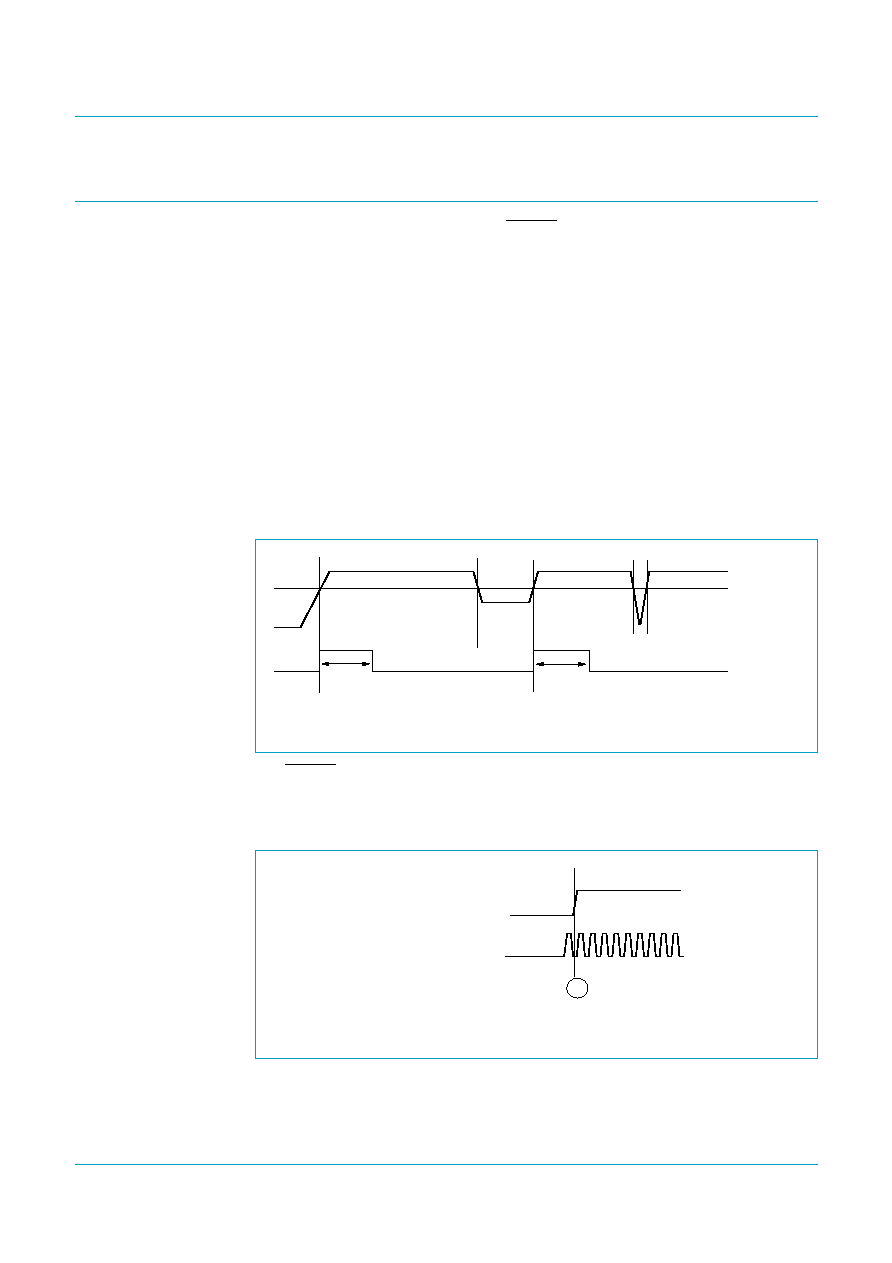
Philips Semiconductors
ISP1161A1
USB single-chip host and device controller
Product data
Rev. 03 -- 23 December 2004
112 of 136
9397 750 13961
© Koninklijke Philips Electronics N.V. 2004. All rights reserved.
16. Power-on reset (POR)
When V
CC
is directly connected to the RESET pin, the internal pulse width (t
PORP
) will
be typically (600 ns to 1000 ns)
+
X, when V
CC
is 3.3 V. X depends on how fast V
CC
is
rising with respect to V
trip
(2.03 V). The time X is decided by the external power
supply circuit.
To give a better view of the functionality,
Figure 49
shows a possible curve of
V
CC(POR)
with dips at t2t3 and t4t5. If the dip at t4t5 is too short (that is,
<
11
µ
s),
the internal POR pulse will not react and will remain LOW. The internal POR starts
with a 1 at t0. At t1, the detector will see the passing of the trip level and a delay
element will add another t
PORP
before it drops to 0.
The internal POR pulse will be generated whenever V
CC(POR)
drops below V
trip
for
more than 11
µ
s.
Even if V
CC
is 5.0 V, V
trip
still remains at 2.03 V. This is because the 5 V tolerant pads
and on-chip voltage regulator ensure that 3.3 V is going to the internal POR circuitry
by clipping the voltage above 3.3 V.
The RESET pin can be either connected to V
CC
(using the internal POR circuit) or
externally controlled (by the micro, ASIC, and so on).
Figure 50
shows the availability of the clock with respect to the external POR.
(1) PORP = power-on reset pulse.
Fig 49. Internal POR timing.
Stable external clock is available at A.
Fig 50. Clock with respect to the external POR.
004aaa389
VBAT(POR)
t0
t1
t2
t3
t4
t5
Vtrip
t
PORP
PORP(1)
t
PORP
POR
EXTERNAL CLOCK
A
004aaa365

Philips Semiconductors
ISP1161A1
USB single-chip host and device controller
Product data
Rev. 03 -- 23 December 2004
113 of 136
9397 750 13961
© Koninklijke Philips Electronics N.V. 2004. All rights reserved.
17. Limiting values
[1]
Equivalent to discharging a 100 pF capacitor via a 1.5 k
resistor (Human Body Model).
18. Recommended operating conditions
[1]
5 V tolerant.
Table 110: Absolute maximum ratings
In accordance with the Absolute Maximum Rating System (IEC 60134).
Symbol
Parameter
Conditions
Min
Max
Unit
V
CC(5V)
supply voltage on pin V
CC
-
0.5
+
6.0
V
V
CC(3.3V)
supply voltage on pin V
reg(3.3)
-
0.5
+
4.6
V
V
I
input voltage
-
0.5
+
6.0
V
I
lu
latch-up current
V
I
< 0 or V
I
> V
CC
-
100
mA
V
esd
electrostatic discharge voltage
I
LI
< 1
µ
A
[1]
-
2000
+
2000
V
T
stg
storage temperature
-
60
+
150
°
C
Table 111: Recommended operating conditions
Symbol
Parameter
Conditions
Min
Typ
Max
Unit
V
CC
supply voltage
with internal regulator
4.0
5.0
5.5
V
internal regulator bypass
3.0
3.3
3.6
V
V
I
input voltage
[1]
0
V
CC
5.5
V
V
I(AI/O)
input voltage on analog I/O pins (D
+
/D
-
)
0
-
3.6
V
V
O(od)
open-drain output pull-up voltage
0
-
V
CC
V
T
amb
ambient temperature
-
40
-
+
85
°
C

Philips Semiconductors
ISP1161A1
USB single-chip host and device controller
Product data
Rev. 03 -- 23 December 2004
114 of 136
9397 750 13961
© Koninklijke Philips Electronics N.V. 2004. All rights reserved.
19. Static characteristics
[1]
For typical values T
amb
= 25
°
C.
[2]
In `suspend' mode, the minimum voltage is 2.7 V.
Table 112: Static characteristics; supply pins
V
CC
= 3.0 V to 3.6 V or 4.0 V to 5.5 V; V
GND
= 0 V; T
amb
=
-
40
°
C to
+
85
°
C; unless otherwise specified.
Symbol
Parameter
Conditions
Min
Typ
[1]
Max
Unit
V
CC
= 5 V
V
reg(3.3)
internal regulator output
typical at T
amb
= 25
°
C
[2]
3.0
3.3
3.6
V
I
CC
operating supply current
typical at T
amb
= 25
°
C
-
47
-
mA
I
CC(susp
)
suspend supply current
typical at T
amb
= 25
°
C
-
40
500
µ
A
I
CC(HC
)
operating supply current for HC DC is suspended;
typical at T
amb
= 25
°
C
-
22
-
mA
I
CC(DC
)
operating supply current for DC HC is suspended;
typical at T
amb
= 25
°
C
-
18
-
mA
V
CC
= 3.3 V
I
CC
operating supply current
typical at T
amb
= 25
°
C
-
50
-
mA
I
CC(susp
)
suspend supply current
typical at T
amb
= 25
°
C
-
150
500
µ
A
I
CC(HC
)
operating supply current for HC DC is suspended;
typical at T
amb
= 25
°
C
-
22
-
mA
I
CC(DC
)
operating supply current for DC HC is suspended;
typical at T
amb
= 25
°
C
-
18
-
mA
Table 113: Static characteristics: digital pins
V
CC
= 3.0 V to 3.6 V or 4.0 V to 5.5 V; V
GND
= 0 V; T
amb
=
-
40
°
C to
+
85
°
C; unless otherwise specified.
Symbol
Parameter
Conditions
Min
Typ
Max
Unit
V
trip
overcurrent detection trip
voltage
-
75
-
mV
Input levels
V
IL
LOW-level input voltage
-
-
0.8
V
V
IH
HIGH-level input voltage
2.0
-
-
V
Schmitt trigger inputs
V
th(LH)
positive-going threshold
voltage
1.4
-
1.9
V
V
th(HL)
negative-going threshold
voltage
0.9
-
1.5
V
V
hys
hysteresis voltage
0.4
-
0.7
V
Output levels
V
OL
LOW-level output voltage
I
OL
= 4 mA
-
-
0.4
V
I
OL
= 20
µ
A
-
-
0.1
V
V
OH
HIGH-level output voltage
I
OH
= 4 mA
[1]
2.4
-
-
V
I
OH
= 20
µ
A
V
reg(3.3)
-
0.1
-
-
V

Philips Semiconductors
ISP1161A1
USB single-chip host and device controller
Product data
Rev. 03 -- 23 December 2004
115 of 136
9397 750 13961
© Koninklijke Philips Electronics N.V. 2004. All rights reserved.
[1]
Not applicable for open-drain outputs.
[2]
This maximum and minimum values are applicable to transistor input only. The value will be different if internal pull-up or pull-down
resistors are used.
[1]
D
+
is the USB positive data pin; D
-
is the USB negative data pin.
[2]
Includes external resistors of 18
±
1 % on both H_D
+
and H_D
-
.
[3]
In `suspend mode', the minimum voltage is 2.7 V.
Leakage current
I
LI
input leakage current
[2]
-
5
-
+
5
µ
A
C
IN
pin capacitance
pin to GND
-
-
5
pF
Open-drain outputs
I
OZ
OFF-state output current
-
5
-
+
5
µ
A
Table 113: Static characteristics: digital pins
...continued
V
CC
= 3.0 V to 3.6 V or 4.0 V to 5.5 V; V
GND
= 0 V; T
amb
=
-
40
°
C to
+
85
°
C; unless otherwise specified.
Symbol
Parameter
Conditions
Min
Typ
Max
Unit
Table 114: Static characteristics: analog I/O pins (D
+
, D
-
)
V
CC
= 3.0 V to 3.6 V or 4.0 V to 5.5 V; V
GND
= 0 V; T
amb
=
-
40
°
C to
+
85
°
C; unless otherwise specified.
Symbol
Parameter
Conditions
Min
Typ
Max
Unit
Input levels
V
DI
differential input sensitivity
|
V
I(D
+
)
-
V
I(D
-
)
|
[1]
0.2
-
-
V
V
CM
differential common mode voltage includes V
DI
range
0.8
-
2.5
V
V
IL
LOW-level input voltage
-
-
0.8
V
V
IH
HIGH-level input voltage
2.0
-
-
V
Output levels
V
OL
LOW-level output voltage
R
L
= 1.5 k
to
3.6 V
-
-
0.3
V
V
OH
HIGH-level output voltage
R
L
= 15 k
to
GND
2.8
-
3.6
V
Leakage current
I
LZ
OFF-state leakage current
-
-
±
10
µ
A
Capacitance
C
IN
transceiver capacitance
pin to GND
-
-
10
pF
Resistance
R
PD
pull-down resistance on HC's
pins DP/DM
enable internal
resistors
10
-
20
k
R
PU
pull-up resistance on pin D_DP
SoftConnect = ON
1
-
2
k
Z
DRV
driver output impedance
steady-state drive
[2]
29
-
44
Z
INP
input impedance
10
-
-
M
Termination
V
TERM
termination voltage for upstream
port pull-up (R
PU
)
[3]
3.0
-
3.6
V

Philips Semiconductors
ISP1161A1
USB single-chip host and device controller
Product data
Rev. 03 -- 23 December 2004
116 of 136
9397 750 13961
© Koninklijke Philips Electronics N.V. 2004. All rights reserved.
20. Dynamic characteristics
[1]
Dependent on the crystal oscillator start-up time.
[1]
Test circuit; see
Figure 66
.
[2]
Excluding the first transition from Idle state.
[3]
Characterized only, not tested. Limits guaranteed by design.
Table 115: Dynamic characteristics
V
CC
= 3.0 V to 3.6 V or 4.0 V to 5.5 V; V
GND
= 0 V; T
amb
=
-
40
°
C to
+
85
°
C; unless otherwise specified.
Symbol
Parameter
Conditions
Min
Typ
Max
Unit
Reset
t
W(RESET)
pulse width on input RESET
crystal oscillator running
160
-
-
µ
s
crystal oscillator stopped
[1]
-
-
-
ms
Crystal oscillator
f
XTAL
crystal frequency
-
6
-
MHz
R
S
series resistance
-
-
100
C
LOAD
load capacitance
-
18
-
pF
External clock input
t
J
external clock jitter
-
-
500
ps
t
DUTY
clock duty cycle
45
50
55
%
t
CR
, t
CF
rise time and fall time
-
-
3
ns
Table 116: Dynamic characteristics: analog I/O pins (D
+
, D
-
)
[1]
V
CC
= 3.0 V to 3.6 V or 4.0 V to 5.5 V; V
GND
= 0 V; T
amb
=
-
40
°
C to
+
85
°
C; C
L
= 50 pF; R
PU
= 1.5 k
±
5 % on D
+
to V
TERM
;
unless otherwise specified.
Symbol
Parameter
Conditions
Min
Typ
Max
Unit
Driver characteristics
t
FR
rise time
C
L
= 50 pF;
10 % to 90 % of
|
V
OH
-
V
OL
|
4
-
20
ns
t
FF
fall time
C
L
= 50 pF;
90 % to 10 % of
|
V
OH
-
V
OL
|
4
-
20
ns
FRFM
differential rise/fall time
matching (t
FR
/t
FF
)
[2]
90
-
111.11
%
V
CRS
output signal crossover voltage
[2][3]
1.3
-
2.0
V

Philips Semiconductors
ISP1161A1
USB single-chip host and device controller
Product data
Rev. 03 -- 23 December 2004
117 of 136
9397 750 13961
© Koninklijke Philips Electronics N.V. 2004. All rights reserved.
20.1 Programmed I/O timing
·
If you are accessing only the HC, then the HC Programmed I/O timing applies.
·
If you are accessing only the DC, then the DC Programmed I/O timing applies.
·
If you are accessing both the HC and the DC, then the DC Programmed I/O timing
applies.
20.1.1
HC Programmed I/O timing
Table 117: Dynamic characteristics: HC Programmed interface timing
Symbol
Parameter
Conditions
Min
Typ
Max
Unit
t
AS
address set-up time before WR
HIGH
5
-
-
ns
t
AH
address hold time after WR HIGH
8
-
-
ns
Read timing
t
SHSL
first RD/WR after A0 HIGH
300
-
-
ns
t
SLRL
CS LOW to RD LOW
0
-
-
ns
t
RHSH
RD HIGH to CS HIGH
0
-
-
ns
t
RLRH
RD LOW pulse width
33
-
-
ns
t
RHRL
RD HIGH to next RD LOW
110
-
-
ns
T
RC
RD cycle time
143
-
-
ns
t
RHDZ
RD data hold time
3
-
22
ns
t
RLDV
RD LOW to data valid
-
-
32
ns
Write timing
t
WL
WR LOW pulse width
26
-
-
ns
t
WHWL
WR HIGH to next WR LOW
110
-
-
ns
T
WC
WR cycle time
136
-
-
ns
t
SLWL
CS LOW to WR LOW
0
-
-
ns
t
WHSH
WR HIGH to CS HIGH
0
-
-
ns
t
WDSU
WR data set-up time
5
-
-
ns
t
WDH
WR data hold time
8
-
-
ns
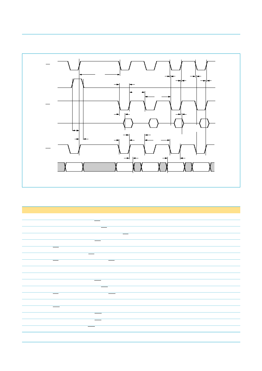
Philips Semiconductors
ISP1161A1
USB single-chip host and device controller
Product data
Rev. 03 -- 23 December 2004
118 of 136
9397 750 13961
© Koninklijke Philips Electronics N.V. 2004. All rights reserved.
20.1.2
DC Programmed I/O timing
Fig 51. HC Programmed interface timing
MGT969
A0
D[15:0]
D[15:0]
WR
RD
CS
data
valid
data
valid
data
valid
data
valid
data
valid
data
valid
data
valid
data
valid
data
valid
tSHSL
tRLRH
tRHRL
tRLDV
tWL
tWHWL
tWDH
tWDSU
TRC
TWC
tRHDZ
tSLRL
tRHSH
tSLWL
tWHSH
t
AH
t
AS
Table 118: Dynamic characteristics: DC Programmed interface timing
Symbol
Parameter
Conditions
Min
Typ
Max
Unit
Read timing (see
Figure 52
)
t
RHAX
address hold time after RD HIGH
0
-
-
ns
t
AVRL
address set-up time before RD LOW
0
-
-
ns
t
SHDZ
data outputs high-impedance time after CS HIGH
-
-
3
ns
t
RHSH
chip deselect time after RD HIGH
0
-
-
ns
t
RLRH
RD pulse width
25
-
-
ns
t
RLDV
data valid time after RD LOW
-
-
22
ns
t
SHRL
CS HIGH until next ISP1161A1 RD
120
-
-
ns
t
SHRL
+ t
RLRH
read cycle time
180
-
-
ns
Write timing (see
Figure 53
)
t
WHAX
address hold time after WR HIGH
1
-
-
ns
t
AVWL
address set-up time before WR LOW
0
-
-
ns
t
SHWL
CS HIGH until next ISP1161A1 WR
120
-
-
ns
t
SHWL
+ t
WLWH
write cycle time
180
-
-
ns
t
WLWH
WR pulse width
22
-
-
ns
t
WHSH
chip deselect time after WR HIGH
0
-
-
ns
t
DVWH
data set-up time before WR HIGH
5
-
-
ns
t
WHDZ
data hold time after WR HIGH
3
-
-
ns
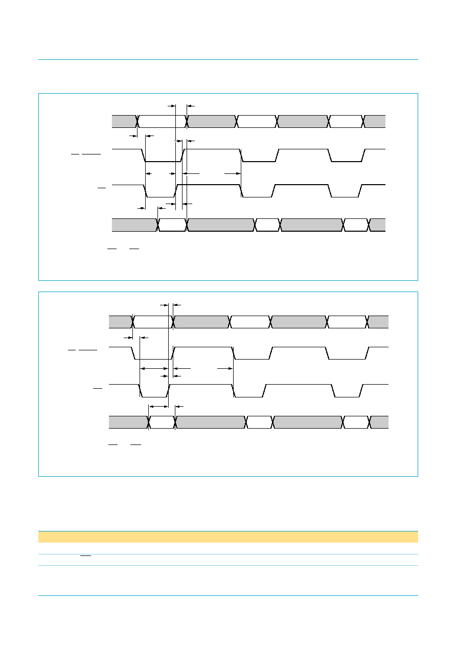
Philips Semiconductors
ISP1161A1
USB single-chip host and device controller
Product data
Rev. 03 -- 23 December 2004
119 of 136
9397 750 13961
© Koninklijke Philips Electronics N.V. 2004. All rights reserved.
20.2 DMA timing
20.2.1
HC single-cycle DMA timing
(1) For t
SHRL
both CS and RD must be de-asserted.
(2) Programmable polarity: shown as active LOW.
Fig 52. DC Programmed interface read timing (I/O and 8237 compatible DMA).
004aaa105
A0
tRHAX
tAVRL
tRLRH
tRLDV
tSHDZ
tSHRL
(1)
D[15:0]
RD
CS/DACK2
(2)
tRHSH
(1) For t
SHWL
both CS and WR must be de-asserted.
(2) Programmable polarity: shown as active LOW.
Fig 53. DC Programmed interface write timing (I/O and 8237 compatible DMA).
004aaa106
CS/DACK2
(2)
A0
D[15:0]
WR
tWHAX
tAVWL
tWHDZ
tDVWH
tWLWH
tWHSH
tSHWL
(1)
Table 119: Dynamic characteristics: HC single-cycle DMA timing
Symbol
Parameter
Conditions
Min
Typ
Max
Unit
Read/write timing
t
RLRH
RD pulse width
33
-
-
ns
t
RLDV
read process data set-up time
26
-
-
ns
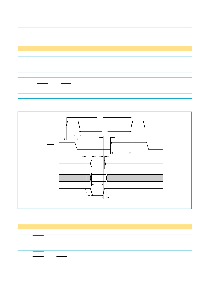
Philips Semiconductors
ISP1161A1
USB single-chip host and device controller
Product data
Rev. 03 -- 23 December 2004
120 of 136
9397 750 13961
© Koninklijke Philips Electronics N.V. 2004. All rights reserved.
[1]
t
RHAL
+ t
DS
+t
ALRL
.
20.2.2
HC burst mode DMA timing
t
RHDZ
read process data hold time
0
-
20
ns
t
WSU
write process data set-up time
5
-
-
ns
t
WHD
write process data hold time
0
-
-
ns
t
AHRH
DACK1 HIGH to DREQ1 HIGH
72
-
-
ns
t
ALRL
DACK1 LOW to DREQ1 LOW
-
-
21
ns
T
DC
DREQ1 cycle
[1]
-
-
-
ns
t
SHAH
RD/WR HIGH to DACK1 HIGH
0
-
-
ns
t
RHAL
DREQ1 HIGH to DACK1 LOW
0
-
-
ns
t
DS
DREQ1 pulse spacing
146
-
-
ns
Table 119: Dynamic characteristics: HC single-cycle DMA timing
...continued
Symbol
Parameter
Conditions
Min
Typ
Max
Unit
Fig 54. HC single-cycle DMA timing.
004aaa107
DREQ1
DACK1
D[15:0]
(read)
D[15:0]
(write)
RD or WR
tDS
tAHRH
TDC
data
valid
data
valid
tALRL
tRHAL
tWHD
tWSU
tRLDV
tRHDZ
tSHAH
Table 120: Dynamic characteristics: HC burst mode DMA timing
Symbol
Parameter
Conditions
Min
Typ
Max
Unit
Read/write timing (for 4-cycle and 8-cycle burst mode)
t
RLRH
WR/RD LOW pulse width
42
-
-
ns
t
RHRL
WR/RD HIGH to next WR/RD LOW
60
-
-
ns
T
RC
WR/RD cycle
102
-
-
ns
t
SLRL
RD/WR LOW to DREQ1 LOW
22
-
64
ns
t
SHAH
RD/WR HIGH to DACK1 HIGH
0
-
-
ns
t
SLAL
DREQ1 HIGH to DACK1 LOW
0
-
ns
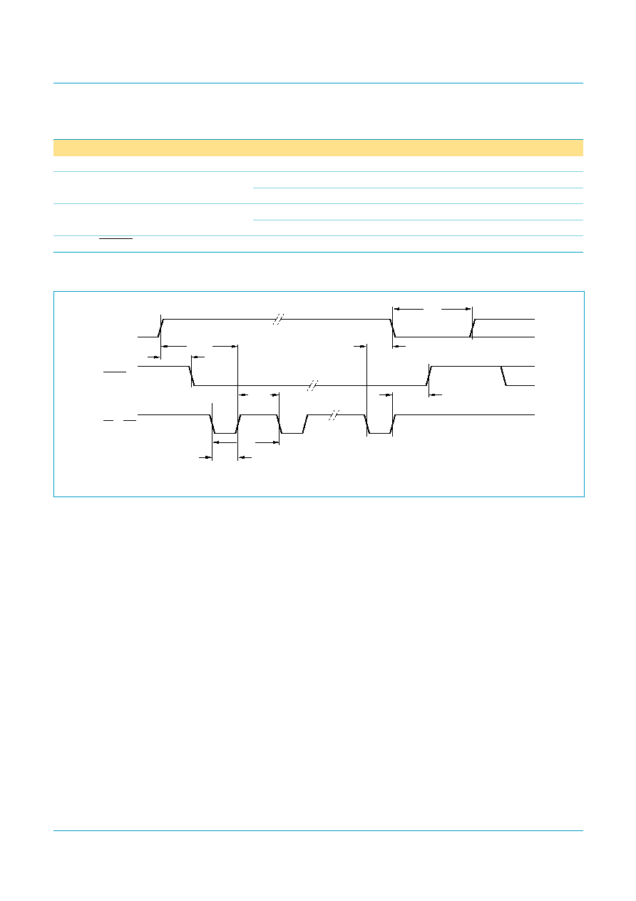
Philips Semiconductors
ISP1161A1
USB single-chip host and device controller
Product data
Rev. 03 -- 23 December 2004
121 of 136
9397 750 13961
© Koninklijke Philips Electronics N.V. 2004. All rights reserved.
[1]
t
SLAL
+ (4 or 8)t
RC
+ t
DS
.
T
DC
DREQ1 cycle
[1]
-
-
-
ns
t
DS(read)
DREQ1 pulse spacing (read)
4-cycle burst mode
105
-
-
ns
8-cycle burst mode
150
-
-
ns
t
DS(write)
DREQ1 pulse spacing (write)
4-cycle burst mode
72
-
-
ns
8-cycle burst mode
167
-
-
ns
t
RLIS
RD/WR LOW to EOT LOW
0
-
-
ns
Table 120: Dynamic characteristics: HC burst mode DMA timing
...continued
Symbol
Parameter
Conditions
Min
Typ
Max
Unit
Fig 55. HC burst mode DMA timing.
004aaa108
tRHRL
tDS
tRHSH
DREQ1
DACK1
RD or WR
tSLRL
tSHAH
tRLRH
TRC
tRHAL
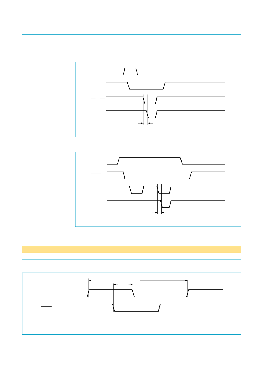
Philips Semiconductors
ISP1161A1
USB single-chip host and device controller
Product data
Rev. 03 -- 23 December 2004
122 of 136
9397 750 13961
© Koninklijke Philips Electronics N.V. 2004. All rights reserved.
20.2.3
External EOT timing for HC single-cycle DMA
20.2.4
External EOT timing for HC burst mode DMA
20.2.5
DC single-cycle DMA timing (8237 mode)
Fig 56. External EOT timing for HC single-cycle DMA.
004aaa109
DREQ1
DACK1
EOT
tRLIS
>
0 ns
RD or WR
Fig 57. External EOT timing for HC burst mode DMA.
004aaa110
DREQ1
DACK1
EOT
tRLIS
>
0 ns
RD or WR
Table 121: Dynamic characteristics: DC single-cycle DMA timing (8237 mode)
Symbol
Parameter
Conditions
Min
Typ
Max
Unit
t
ASRP
DREQ2 off after DACK2 on
-
-
40
ns
T
cy(DREQ2)
cycle time signal DREQ2
180
-
-
ns
(1) Programmable polarity: shown as active LOW.
Fig 58. DC single-cycle DMA timing (8237 mode).
004aaa111
DREQ2
DACK2
(1)
tASRP
TRC
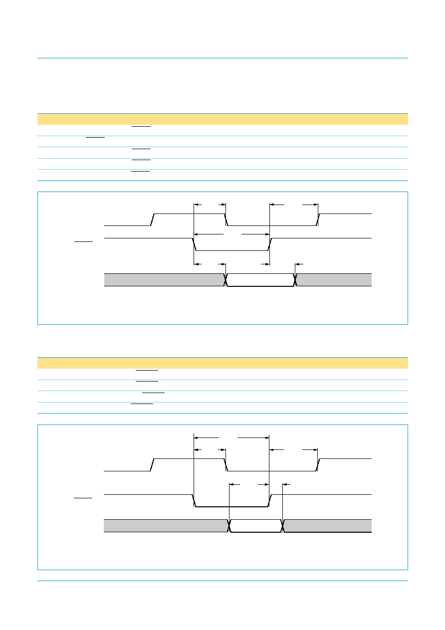
Philips Semiconductors
ISP1161A1
USB single-chip host and device controller
Product data
Rev. 03 -- 23 December 2004
123 of 136
9397 750 13961
© Koninklijke Philips Electronics N.V. 2004. All rights reserved.
20.2.6
DC single-cycle DMA read timing in DACK-only mode
20.2.7
DC single-cycle DMA write timing in DACK-only mode
Table 122: Dynamic characteristics: DC single-cycle DMA read timing in DACK-only mode
Symbol
Parameter
Conditions
Min
Typ
Max
Unit
t
ASRP
DREQ off after DACK on
-
-
40
ns
t
ASAP
DACK pulse width
25
-
-
ns
t
ASAP
+ t
APRS
DREQ on after DACK off
180
-
-
ns
t
ASDV
data valid after DACK on
-
-
22
ns
t
APDZ
data hold after DACK off
-
-
3
ns
(1) Programmable polarity: shown as active LOW.
Fig 59. DC single-cycle DMA read timing in DACK-only mode.
004aaa112
DACK2
(1)
DREQ2
tASRP
tAPRS
tASDV
tAPDZ
DATA
tASAP
Table 123: Dynamic characteristics: DC single-cycle DMA write timing in DACK-only mode
Symbol
Parameter
Conditions
Min
Typ
Max
Unit
t
ASRP
DREQ2 off after DACK2 on
-
-
40
ns
t
ASAP
+ t
APRS
DREQ2 on after DACK2 off
180
-
-
ns
t
DVAP
data set-up before DACK2 off
5
-
-
ns
t
APDZ
data hold after DACK2 off
3
-
-
ns
(1) Programmable polarity: shown as active LOW.
Fig 60. DC single-cycle DMA write timing in DACK-only mode.
004aaa113
DACK2
(1)
DREQ2
tASRP
tAPRS
tASDV
tAPDZ
DATA
tASAP
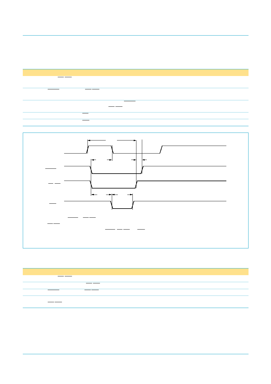
Philips Semiconductors
ISP1161A1
USB single-chip host and device controller
Product data
Rev. 03 -- 23 December 2004
124 of 136
9397 750 13961
© Koninklijke Philips Electronics N.V. 2004. All rights reserved.
20.2.8
EOT timing in DC single-cycle DMA
20.2.9
DC burst mode DMA timing
Table 124: Dynamic characteristics: EOT timing in DC single-cycle DMA
Symbol
Parameter
Conditions
Min
Typ
Max
Unit
t
RSIH
input RD/WR HIGH after DREQ
on
22
-
-
ns
t
IHAP
DACK off after input RD/WR
HIGH
0
-
-
ns
t
EOT
EOT pulse width
EOT on; DACK on;
RD/WR LOW
22
-
-
ns
t
RLIS
input EOT on after RD LOW
-
-
89
ns
t
WLIS
input EOT on after WR LOW
-
89
ns
(1) t
ASRP
starts from DACK or RD/WR going LOW, whichever occurs later.
(2) The RD/WR signals are not used in DACK-only DMA mode.
(3) The EOT condition is considered valid if DACK, RD/WR and EOT are all active (= LOW).
(4) Programmable polarity: shown as active LOW.
Fig 61. EOT timing in DC single-cycle DMA.
004aaa114
DREQ2
tRSIH
tIHAP
tASRP
(1)
tEOT
(3)
tRLIS
tWLIS
EOT
(4)
DACK2
(4)
RD/WR
(2)
Table 125: Dynamic characteristics: DC burst mode DMA timing
Symbol
Parameter
Conditions
Min
Typ
Max
Unit
t
RSIH
input RD/WR HIGH after DREQ on
22
-
-
ns
t
ILRP
DREQ off after input RD/WR LOW
-
-
60
ns
t
IHAP
DACK off after input RD/WR HIGH
0
-
-
ns
t
IHIL
DMA burst repeat interval (input
RD/WR HIGH to LOW)
180
-
-
ns
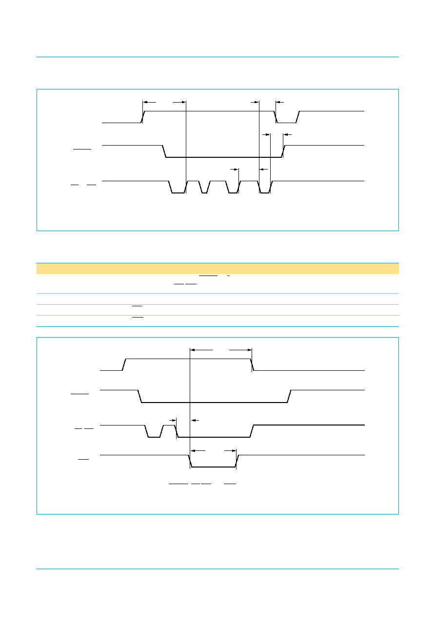
Philips Semiconductors
ISP1161A1
USB single-chip host and device controller
Product data
Rev. 03 -- 23 December 2004
125 of 136
9397 750 13961
© Koninklijke Philips Electronics N.V. 2004. All rights reserved.
20.2.10
EOT timing in DC burst mode DMA
(1) Programmable polarity: shown as active LOW.
Fig 62. DC burst mode DMA timing.
004aaa115
DACK2
(1)
DREQ2
tRSIH
tILRP
tIHIL
tIHAP
RD or WR
Table 126: Dynamic characteristics: EOT timing in DC burst mode DMA
Symbol
Parameter
Conditions
Min
Typ
Max
Unit
t
EOT
EOT pulse width
EOT on; DACK on;
RD/WR LOW
22
-
-
ns
t
ISRP
DREQ off after input EOT on
-
-
40
ns
t
RLIS
input EOT on after RD LOW
-
-
89
ns
t
WLIS
input EOT on after WR LOW
-
-
89
ns
(1) The EOT condition is considered valid if DACK2, RD/WR and EOT are all active (= LOW).
(2) Programmable polarity: shown as active LOW.
Fig 63. EOT timing in DC burst mode DMA.
004aaa116
DACK2
(2)
DREQ2
tISRP
tEOT
(1)
RD/WR
EOT
(2)
tRLIS
tWLIS
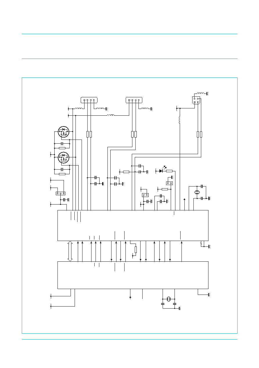
Philips Semiconductors
ISP1161A1
USB single-chip host and device controller
Product data
Rev. 03 -- 23 December 2004
126 of 136
9397 750 13961
© Koninklijke Philips Electronics N.V. 2004. All rights reserved.
21. Application information
21.1 Typical interface circuit
(1) For MOSFET, R
DSon
= 150 m
.
(2) 470
assuming that V
CC
is 5.0 V.
Fig 64. Typical interface circuit to Hitachi SH-3 (SH7709) RISC processor.
004aaa192
470
(2)
LED
FB4
FB6
FB3
FB2
FB1
22
(2
×
)
18 pF
18 pF
+
5 V
+
3.3 V
+
3.3 V
+
5 V
V
DD
+
5 V
+
5 V
Vbus_DN2
Vbus_DN1
+
3.3 V
+
5 V
SH7709
A1
A0
MOSFET (2
×
)
(1)
USB
downstream
port #1
USB
downstream
port #2
D
[15:0
]
D
[15:0
]
A2
A1
DREQ0
DREQ1
DACK0
DACK1
DREQ1
DREQ2
CS5
CS
RD
RD
R
D/W
R
W
R
DACK1
DACK2
EOT
PTC0
H_WAKEUP
PTC1
H_SUSPEND
PTC2
D_WAKEUP
PTC3
D_SUSPEND
GND
XTAL2
EXTAL2
32
kHz
6 MHz
XTAL
EXTAL
DGND
AGND
IRQ2
INT1
IRQ3
INT2
RSTOUT
RESET
ISP1161A1
CLKOUT
CLKOUT
H_OC1
H_OC2
H_PSW2
H_PSW1
V
CC
V
reg(3.3)
V
hold1
V
hold2
H_DM1
H_DP1
H_DM2
H_DP2
D_DM
D_DP
NDP_SEL
GL
D_VBUS
CLKOUT
XTAL2
XTAL1
V
reg
V
DD
V
DD
+
3.3 V
USB
upstream
port
22
(2
×
)
47 pF
(2
×
)
Vbus_UP
FB5
22
(2
×
)
7
1.5 k
V
reg
47 pF
(2
×
)
47 pF
(2
×
)

Philips Semiconductors
ISP1161A1
USB single-chip host and device controller
Product data
Rev. 03 -- 23 December 2004
127 of 136
9397 750 13961
© Koninklijke Philips Electronics N.V. 2004. All rights reserved.
21.2 Interfacing a ISP1161A1 with a SH7709 RISC processor
This section shows a typical interface circuit between the ISP1161A1 and a RISC
processor. The Hitachi SH-3 series RISC processor SH7709 is used as the example.
The main ISP1161A1 signals to be taken into consideration for connecting to a
SH7709 RISC processor are:
·
A 16-bit data bus: D[15:0] for the ISP1161A1. The ISP1161A1 is `little endian'
compatible.
·
Two address lines A1 and A0 are needed for a complete addressing of the
ISP1161A1 internal registers:
A1 = 0 and A0 = 0 will select the Data Port of the Host Controller
A1 = 0 and A0 = 1 will select the Command Port of the Host Controller
A1 = 1 and A0 = 0 will select the Data Port of the Device Controller
A1 = 1 and A0 = 1 will select the Command Port of the Device Controller
·
The CS line is used for chip selection of the ISP1161A1 in a certain address range
of the RISC system. This signal is active LOW.
·
RD and WR are common read and write signals. These signals are active LOW.
·
There are two DMA channel standard control lines:
DREQ1 and DACK1
DREQ2 and DACK2
(in each case one channel is used by the HC and the other channel is used by
the DC). These signals have programmable active levels.
·
Two interrupt lines: INT1 (used by the HC) and INT2 (used by the device
controller). Both have programmable level/edge and polarity (active HIGH or
LOW).
·
The internal 15 k
pull-down resistors are used for the HC's two USB downstream
ports.
·
The RESET signal is active LOW.
Remark: SH7709's system clock input is for reference only. Refer to SH7709's
specification for its actual use.
The ISP1161A1 can work under either 3.3 V or 5.0 V power supply; however, its
internal core works at 3.3 V. When using 3.3 V as the power supply input, the internal
DC/DC regulator will be bypassed. It is best to connect all four power supply pins
(V
CC
, V
reg(3.3)
, V
hold1
and V
hold2
) to the 3.3 V power supply (for more information, see
Section 14
). All of the ISP1161A1's I/O pins are 5 V tolerant. This feature allows the
ISP1161A1 the flexibility to be used in an embedded system under either a 3.3 V or a
5 V power supply.
A typical SH7709 interface circuit is shown in
Figure 64
.
21.3 Typical software model
This section shows a typical software requirement for an embedded system that
incorporates the ISP1161A1. The software model for a Digital Still Camera (DSC) is
used as the example for illustration (as shown in
Figure 65
). Two components of
system software are required to make full use of the features in the ISP1161A1: the
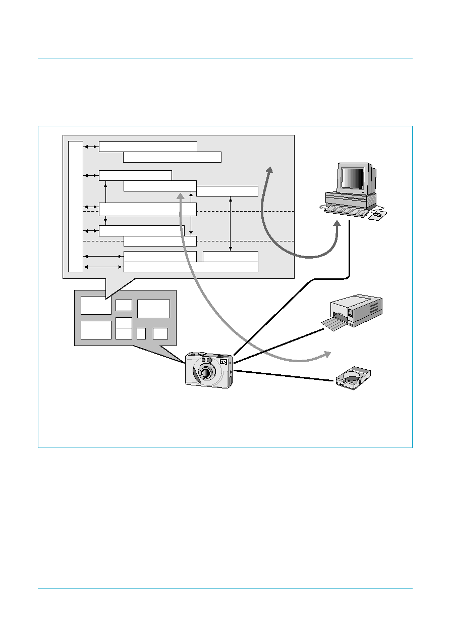
Philips Semiconductors
ISP1161A1
USB single-chip host and device controller
Product data
Rev. 03 -- 23 December 2004
128 of 136
9397 750 13961
© Koninklijke Philips Electronics N.V. 2004. All rights reserved.
host stack and the device stack. The device stack provides API directly to the
application task for device function; the host stack provides API for Class driver and
device driver, both of which provide API for application tasks for host function.
Fig 65. ISP1161A1 software model for DSC application.
Printer
PC
Flash card
Reader/
Writer
USB Upstream
USB Downstream
Digital Still Camera
RISC
ROM
RAM
ISP1161A1
LEN
CONTROL
004aaa193
MECHANISM CONTROL TASK
IMAGE PROCESSING TASKS
FILE MANAGEMENT
OS
PRINTER UI/CONTROL
PRINTING CLASS DRIVER
HOST STACK
DEVICE STACK
USB
host/device
stack
Class
driver
Application
layer
FILE TRANSFER
DEVICE DRIVERS
MASS STORAGE CLASS DRIVER
ISP1161A1 HAL
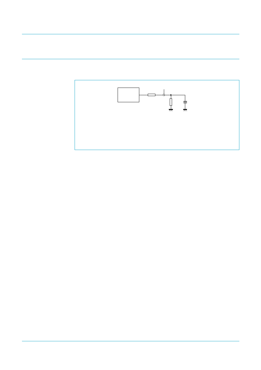
Philips Semiconductors
ISP1161A1
USB single-chip host and device controller
Product data
Rev. 03 -- 23 December 2004
129 of 136
9397 750 13961
© Koninklijke Philips Electronics N.V. 2004. All rights reserved.
22. Test information
The dynamic characteristics of the analog I/O ports (D
+
and D
-)
as listed in
Table 116
were determined using the circuit shown in
Figure 66
.
Load capacitance:
C
L
= 50 pF (full-speed mode).
Speed:
full-speed mode only: internal 1.5 k
pull-up resistor on D_DP.
Fig 66. Load impedance for pins D_DP and D_DM.
MGT967
15 k
22
test point
CL
50 pF
D.U.T.
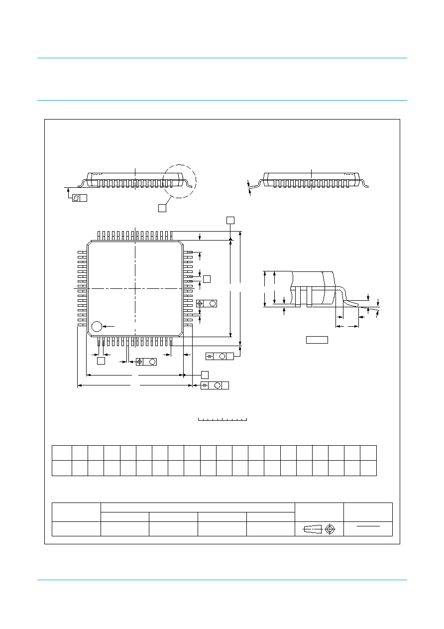
Philips Semiconductors
ISP1161A1
USB single-chip host and device controller
Product data
Rev. 03 -- 23 December 2004
130 of 136
9397 750 13961
© Koninklijke Philips Electronics N.V. 2004. All rights reserved.
23. Package outline
Fig 67. LQFP64 (SOT314-2) package outline.
UNIT
A
max.
A
1
A
2
A
3
b
p
c
E
(1)
e
H
E
L
L
p
Z
y
w
v
REFERENCES
OUTLINE
VERSION
EUROPEAN
PROJECTION
ISSUE DATE
IEC
JEDEC
JEITA
mm
1.6
0.20
0.05
1.45
1.35
0.25
0.27
0.17
0.18
0.12
10.1
9.9
0.5
12.15
11.85
1.45
1.05
7
0
o
o
0.12
0.1
1
0.2
DIMENSIONS (mm are the original dimensions)
Note
1. Plastic or metal protrusions of 0.25 mm maximum per side are not included.
0.75
0.45
SOT314-2
MS-026
136E10
00-01-19
03-02-25
D
(1)
(1)
(1)
10.1
9.9
H
D
12.15
11.85
E
Z
1.45
1.05
D
b
p
e
E
A
1
A
L
p
detail X
L
(A )
3
B
16
c
D
H
b
p
E
H
A
2
v
M
B
D
Z D
A
Z E
e
v
M
A
X
1
64
49
48
33
32
17
y
pin 1 index
w
M
w
M
0
2.5
5 mm
scale
LQFP64: plastic low profile quad flat package; 64 leads; body 10 x 10 x 1.4 mm
SOT314-2
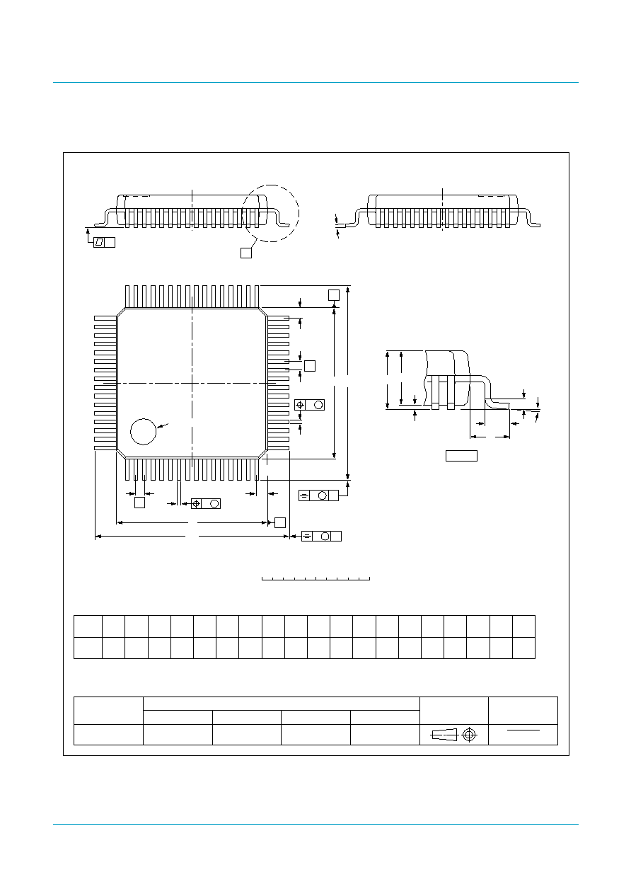
Philips Semiconductors
ISP1161A1
USB single-chip host and device controller
Product data
Rev. 03 -- 23 December 2004
131 of 136
9397 750 13961
© Koninklijke Philips Electronics N.V. 2004. All rights reserved.
Fig 68. LQFP64 (SOT414-1) package outline.
UNIT
A
max.
A
1
A
2
A
3
b
p
c
E
(1)
e
H
E
L
L
p
Z
y
w
v
REFERENCES
OUTLINE
VERSION
EUROPEAN
PROJECTION
ISSUE DATE
IEC
JEDEC
JEITA
mm
1.6
0.15
0.05
1.45
1.35
0.25
0.23
0.13
0.20
0.09
7.1
6.9
0.4
9.15
8.85
0.64
0.36
7
0
o
o
0.08
0.08
1
0.2
DIMENSIONS (mm are the original dimensions)
Note
1. Plastic or metal protrusions of 0.25 mm maximum per side are not included.
0.75
0.45
SOT414-1
136E06
MS-026
00-01-19
03-02-20
D
(1)
(1)
(1)
7.1
6.9
H
D
9.15
8.85
E
Z
0.64
0.36
D
b
p
e
E
A
1
A
L
p
detail X
L
(A )
3
B
16
c
D
H
b
p
E
H
A
2
v
M
B
D
Z D
A
Z E
e
v
M
A
X
1
64
49
48
33
32
17
y
pin 1 index
w
M
w
M
0
2.5
5 mm
scale
LQFP64: plastic low profile quad flat package; 64 leads; body 7 x 7 x 1.4 mm
SOT414-1

Philips Semiconductors
ISP1161A1
USB single-chip host and device controller
Product data
Rev. 03 -- 23 December 2004
132 of 136
9397 750 13961
© Koninklijke Philips Electronics N.V. 2004. All rights reserved.
24. Soldering
24.1 Introduction to soldering surface mount packages
This text gives a very brief insight to a complex technology. A more in-depth account
of soldering ICs can be found in our
Data Handbook IC26; Integrated Circuit
Packages (document order number 9398 652 90011).
There is no soldering method that is ideal for all surface mount IC packages. Wave
soldering can still be used for certain surface mount ICs, but it is not suitable for fine
pitch SMDs. In these situations reflow soldering is recommended. In these situations
reflow soldering is recommended.
24.2 Reflow soldering
Reflow soldering requires solder paste (a suspension of fine solder particles, flux and
binding agent) to be applied to the printed-circuit board by screen printing, stencilling
or pressure-syringe dispensing before package placement. Driven by legislation and
environmental forces the worldwide use of lead-free solder pastes is increasing.
Several methods exist for reflowing; for example, convection or convection/infrared
heating in a conveyor type oven. Throughput times (preheating, soldering and
cooling) vary between 100 and 200 seconds depending on heating method.
Typical reflow peak temperatures range from 215 to 270
°
C depending on solder
paste material. The top-surface temperature of the packages should preferably be
kept:
·
below 225
°
C (SnPb process) or below 245
°
C (Pb-free process)
for all BGA, HTSSON..T and SSOP..T packages
for packages with a thickness
2.5 mm
for packages with a thickness < 2.5 mm and a volume
350 mm
3
so called
thick/large packages.
·
below 240
°
C (SnPb process) or below 260
°
C (Pb-free process) for packages with
a thickness < 2.5 mm and a volume < 350 mm
3
so called small/thin packages.
Moisture sensitivity precautions, as indicated on packing, must be respected at all
times.
24.3 Wave soldering
Conventional single wave soldering is not recommended for surface mount devices
(SMDs) or printed-circuit boards with a high component density, as solder bridging
and non-wetting can present major problems.
To overcome these problems the double-wave soldering method was specifically
developed.
If wave soldering is used the following conditions must be observed for optimal
results:
·
Use a double-wave soldering method comprising a turbulent wave with high
upward pressure followed by a smooth laminar wave.

Philips Semiconductors
ISP1161A1
USB single-chip host and device controller
Product data
Rev. 03 -- 23 December 2004
133 of 136
9397 750 13961
© Koninklijke Philips Electronics N.V. 2004. All rights reserved.
·
For packages with leads on two sides and a pitch (e):
larger than or equal to 1.27 mm, the footprint longitudinal axis is preferred to be
parallel to the transport direction of the printed-circuit board;
smaller than 1.27 mm, the footprint longitudinal axis must be parallel to the
transport direction of the printed-circuit board.
The footprint must incorporate solder thieves at the downstream end.
·
For packages with leads on four sides, the footprint must be placed at a 45
°
angle
to the transport direction of the printed-circuit board. The footprint must
incorporate solder thieves downstream and at the side corners.
During placement and before soldering, the package must be fixed with a droplet of
adhesive. The adhesive can be applied by screen printing, pin transfer or syringe
dispensing. The package can be soldered after the adhesive is cured.
Typical dwell time of the leads in the wave ranges from 3 to 4 seconds at 250
°
C or
265
°
C, depending on solder material applied, SnPb or Pb-free respectively.
A mildly-activated flux will eliminate the need for removal of corrosive residues in
most applications.
24.4 Manual soldering
Fix the component by first soldering two diagonally-opposite end leads. Use a low
voltage (24 V or less) soldering iron applied to the flat part of the lead. Contact time
must be limited to 10 seconds at up to 300
°
C.
When using a dedicated tool, all other leads can be soldered in one operation within
2 to 5 seconds between 270 and 320
°
C.
24.5 Package related soldering information
[1]
For more detailed information on the BGA packages refer to the
(LF)BGA Application Note
(AN01026); order a copy from your Philips Semiconductors sales office.
[2]
All surface mount (SMD) packages are moisture sensitive. Depending upon the moisture content, the
maximum temperature (with respect to time) and body size of the package, there is a risk that internal
or external package cracks may occur due to vaporization of the moisture in them (the so called
popcorn effect). For details, refer to the Drypack information in the
Data Handbook IC26; Integrated
Circuit Packages; Section: Packing Methods.
Table 127: Suitability of surface mount IC packages for wave and reflow soldering
methods
Package
[1]
Soldering method
Wave
Reflow
[2]
BGA, HTSSON..T
[3]
, LBGA, LFBGA, SQFP,
SSOP..T
[3]
, TFBGA, USON, VFBGA
not suitable
suitable
DHVQFN, HBCC, HBGA, HLQFP, HSO, HSOP,
HSQFP, HSSON, HTQFP, HTSSOP, HVQFN,
HVSON, SMS
not suitable
[4]
suitable
PLCC
[5]
, SO, SOJ
suitable
suitable
LQFP, QFP, TQFP
not recommended
[5][6]
suitable
SSOP, TSSOP, VSO, VSSOP
not recommended
[7]
suitable
CWQCCN..L
[8]
, PMFP
[9]
, WQCCN..L
[8]
not suitable
not suitable

Philips Semiconductors
ISP1161A1
USB single-chip host and device controller
Product data
Rev. 03 -- 23 December 2004
134 of 136
9397 750 13961
© Koninklijke Philips Electronics N.V. 2004. All rights reserved.
[3]
These transparent plastic packages are extremely sensitive to reflow soldering conditions and must
on no account be processed through more than one soldering cycle or subjected to infrared reflow
soldering with peak temperature exceeding 217
°
C
±
10
°
C measured in the atmosphere of the reflow
oven. The package body peak temperature must be kept as low as possible.
[4]
These packages are not suitable for wave soldering. On versions with the heatsink on the bottom
side, the solder cannot penetrate between the printed-circuit board and the heatsink. On versions with
the heatsink on the top side, the solder might be deposited on the heatsink surface.
[5]
If wave soldering is considered, then the package must be placed at a 45
°
angle to the solder wave
direction. The package footprint must incorporate solder thieves downstream and at the side corners.
[6]
Wave soldering is suitable for LQFP, QFP and TQFP packages with a pitch (e) larger than 0.8 mm; it
is definitely not suitable for packages with a pitch (e) equal to or smaller than 0.65 mm.
[7]
Wave soldering is suitable for SSOP, TSSOP, VSO and VSOP packages with a pitch (e) equal to or
larger than 0.65 mm; it is definitely not suitable for packages with a pitch (e) equal to or smaller than
0.5 mm.
[8]
Image sensor packages in principle should not be soldered. They are mounted in sockets or delivered
pre-mounted on flex foil. However, the image sensor package can be mounted by the client on a flex
foil by using a hot bar soldering process. The appropriate soldering profile can be provided on
request.
[9]
Hot bar soldering or manual soldering is suitable for PMFP packages.
25. Revision history
Table 128: Revision history
Rev Date
CPCN
Description
03
20041223
200412020
Product data (9397 750 13961)
Modifications:
·
Section 9.8.1 "Using an internal OC detection circuit"
: fourth paragraph, second
sentence, changed source to drain and drain to source
·
Section 11.4 "Suspend and resume"
: updated the entire section
·
Removed Section 20.1 Timing symbols
·
Table 118 "Dynamic characteristics: DC Programmed interface timing"
: changed the
min value of t
RHAX
from 3 ns to 0 ns and of t
WHAX
from 3 ns to 1 ns, and added t
SHRL
and t
SHWL
.
02
20030825
-
Product data (9397 750 11828)
01
20021220
-
Product data (9397 750 10241)

9397 750 13961
Philips Semiconductors
ISP1161A1
USB single-chip host and device controller
© Koninklijke Philips Electronics N.V. 2004. All rights reserved.
Product data
Rev. 03 -- 23 December 2004
135 of 136
Contact information
For additional information, please visit http://www.semiconductors.philips.com.
For sales office addresses, send e-mail to: sales.addresses@www.semiconductors.philips.com.
Fax: +31 40 27 24825
26. Data sheet status
[1]
Please consult the most recently issued data sheet before initiating or completing a design.
[2]
The product status of the device(s) described in this data sheet may have changed since this data sheet was published. The latest information is available on the Internet at
URL http://www.semiconductors.philips.com.
[3]
For data sheets describing multiple type numbers, the highest-level product status determines the data sheet status.
27. Definitions
Short-form specification -- The data in a short-form specification is
extracted from a full data sheet with the same type number and title. For
detailed information see the relevant data sheet or data handbook.
Limiting values definition -- Limiting values given are in accordance with
the Absolute Maximum Rating System (IEC 60134). Stress above one or
more of the limiting values may cause permanent damage to the device.
These are stress ratings only and operation of the device at these or at any
other conditions above those given in the Characteristics sections of the
specification is not implied. Exposure to limiting values for extended periods
may affect device reliability.
Application information -- Applications that are described herein for any
of these products are for illustrative purposes only. Philips Semiconductors
make no representation or warranty that such applications will be suitable for
the specified use without further testing or modification.
28. Disclaimers
Life support -- These products are not designed for use in life support
appliances, devices, or systems where malfunction of these products can
reasonably be expected to result in personal injury. Philips Semiconductors
customers using or selling these products for use in such applications do so
at their own risk and agree to fully indemnify Philips Semiconductors for any
damages resulting from such application.
Right to make changes -- Philips Semiconductors reserves the right to
make changes in the products - including circuits, standard cells, and/or
software - described or contained herein in order to improve design and/or
performance. When the product is in full production (status `Production'),
relevant changes will be communicated via a Customer Product/Process
Change Notification (CPCN). Philips Semiconductors assumes no
responsibility or liability for the use of any of these products, conveys no
licence or title under any patent, copyright, or mask work right to these
products, and makes no representations or warranties that these products are
free from patent, copyright, or mask work right infringement, unless otherwise
specified.
29. Trademarks
ARM7 and ARM9 -- are trademarks of ARM Ltd.
GoodLink -- is a trademark of Koninklijke Philips Electronics N.V.
Hitachi -- is a registered trademark of Hitachi Ltd.
MIPS-based -- is a trademark of MIPS Technologies, Inc.
SoftConnect -- is a trademark of Koninklijke Philips Electronics N.V.
StrongARM -- is a registered trademark of ARM Ltd.
SuperH -- is a trademark of Hitachi Ltd.
Level
Data sheet status
[1]
Product status
[2][3]
Definition
I
Objective data
Development
This data sheet contains data from the objective specification for product development. Philips
Semiconductors reserves the right to change the specification in any manner without notice.
II
Preliminary data
Qualification
This data sheet contains data from the preliminary specification. Supplementary data will be published
at a later date. Philips Semiconductors reserves the right to change the specification without notice, in
order to improve the design and supply the best possible product.
III
Product data
Production
This data sheet contains data from the product specification. Philips Semiconductors reserves the
right to make changes at any time in order to improve the design, manufacturing and supply. Relevant
changes will be communicated via a Customer Product/Process Change Notification (CPCN).

© Koninklijke Philips Electronics N.V. 2004.
Printed in The Netherlands
All rights are reserved. Reproduction in whole or in part is prohibited without the prior
written consent of the copyright owner.
The information presented in this document does not form part of any quotation or
contract, is believed to be accurate and reliable and may be changed without notice. No
liability will be accepted by the publisher for any consequence of its use. Publication
thereof does not convey nor imply any license under patent- or other industrial or
intellectual property rights.
Date of release: 23 December 2004
Document order number: 9397 750 13961
Contents
Philips Semiconductors
ISP1161A1
USB single-chip host and device controller
1
General description . . . . . . . . . . . . . . . . . . . . . . 1
2
Features . . . . . . . . . . . . . . . . . . . . . . . . . . . . . . . 3
3
Applications . . . . . . . . . . . . . . . . . . . . . . . . . . . . 4
4
Ordering information . . . . . . . . . . . . . . . . . . . . . 4
5
Block diagram . . . . . . . . . . . . . . . . . . . . . . . . . . 5
6
Pinning information . . . . . . . . . . . . . . . . . . . . . . 7
6.1
Pinning . . . . . . . . . . . . . . . . . . . . . . . . . . . . . . . 7
6.2
Pin description . . . . . . . . . . . . . . . . . . . . . . . . . 7
7
Functional description . . . . . . . . . . . . . . . . . . 11
7.1
PLL clock multiplier . . . . . . . . . . . . . . . . . . . . . 11
7.2
Bit clock recovery . . . . . . . . . . . . . . . . . . . . . . 11
7.3
Analog transceivers . . . . . . . . . . . . . . . . . . . . 11
7.4
Philips Serial Interface Engine (SIE). . . . . . . . 11
7.5
SoftConnect . . . . . . . . . . . . . . . . . . . . . . . . . . 11
7.6
GoodLink . . . . . . . . . . . . . . . . . . . . . . . . . . . . 12
8
Microprocessor bus interface. . . . . . . . . . . . . 12
8.1
Programmed I/O (PIO) addressing mode . . . . 12
8.2
DMA mode . . . . . . . . . . . . . . . . . . . . . . . . . . . 12
8.3
Control register access by PIO mode . . . . . . . 13
8.4
FIFO buffer RAM access by PIO mode . . . . . 16
8.5
FIFO buffer RAM access by DMA mode. . . . . 17
8.6
Interrupts . . . . . . . . . . . . . . . . . . . . . . . . . . . . 18
9
USB host controller (HC). . . . . . . . . . . . . . . . . 24
9.1
HC's four USB states . . . . . . . . . . . . . . . . . . . 24
9.2
Generating USB traffic . . . . . . . . . . . . . . . . . . 24
9.3
PTD data structure . . . . . . . . . . . . . . . . . . . . . 26
9.4
HC internal FIFO buffer RAM structure . . . . . 29
9.5
HC operational model . . . . . . . . . . . . . . . . . . . 35
9.6
Microprocessor loading. . . . . . . . . . . . . . . . . . 38
9.7
Internal pull-down resistors for downstream
ports. . . . . . . . . . . . . . . . . . . . . . . . . . . . . . . . 38
9.8
OC detection and power switching control . . . 39
9.9
Suspend and wake-up . . . . . . . . . . . . . . . . . . 41
10
HC registers . . . . . . . . . . . . . . . . . . . . . . . . . . . 44
10.1
HC control and status registers . . . . . . . . . . . 45
10.2
HC frame counter registers. . . . . . . . . . . . . . . 52
10.3
HC Root Hub registers . . . . . . . . . . . . . . . . . . 55
10.4
HC DMA and interrupt control registers . . . . . 65
10.5
HC miscellaneous registers . . . . . . . . . . . . . . 70
10.6
HC buffer RAM control registers . . . . . . . . . . . 72
11
USB device controller (DC) . . . . . . . . . . . . . . . 77
11.1
DC data transfer operation . . . . . . . . . . . . . . . 77
11.2
Device DMA transfer. . . . . . . . . . . . . . . . . . . . 78
11.3
Endpoint descriptions . . . . . . . . . . . . . . . . . . . 79
11.4
Suspend and resume . . . . . . . . . . . . . . . . . . . 82
12
DC DMA transfer . . . . . . . . . . . . . . . . . . . . . . . 85
12.1
Selecting an endpoint for DMA transfer . . . . . 85
12.2
8237 compatible mode . . . . . . . . . . . . . . . . . . 86
12.3
DACK-only mode . . . . . . . . . . . . . . . . . . . . . . 87
12.4
End-Of-Transfer conditions. . . . . . . . . . . . . . . 88
13
DC commands and registers . . . . . . . . . . . . . 90
13.1
Initialization commands . . . . . . . . . . . . . . . . . 92
13.2
Data flow commands . . . . . . . . . . . . . . . . . . . 99
13.3
General commands . . . . . . . . . . . . . . . . . . . 103
14
Power supply . . . . . . . . . . . . . . . . . . . . . . . . . 109
15
Crystal oscillator and LazyClock . . . . . . . . . 109
16
Power-on reset (POR) . . . . . . . . . . . . . . . . . . 112
17
Limiting values . . . . . . . . . . . . . . . . . . . . . . . 113
18
Recommended operating conditions . . . . . 113
19
Static characteristics . . . . . . . . . . . . . . . . . . 114
20
Dynamic characteristics . . . . . . . . . . . . . . . . 116
20.1
Programmed I/O timing . . . . . . . . . . . . . . . . 117
20.2
DMA timing. . . . . . . . . . . . . . . . . . . . . . . . . . 119
21
Application information . . . . . . . . . . . . . . . . 126
21.1
Typical interface circuit . . . . . . . . . . . . . . . . . 126
21.2
Interfacing a ISP1161A1 with a SH7709
RISC processor. . . . . . . . . . . . . . . . . . . . . . 127
21.3
Typical software model . . . . . . . . . . . . . . . . . 127
22
Test information. . . . . . . . . . . . . . . . . . . . . . . 129
23
Package outline . . . . . . . . . . . . . . . . . . . . . . . 130
24
Soldering . . . . . . . . . . . . . . . . . . . . . . . . . . . . 132
24.1
Introduction to soldering surface mount
packages . . . . . . . . . . . . . . . . . . . . . . . . . . . 132
24.2
Reflow soldering. . . . . . . . . . . . . . . . . . . . . . 132
24.3
Wave soldering. . . . . . . . . . . . . . . . . . . . . . . 132
24.4
Manual soldering . . . . . . . . . . . . . . . . . . . . . 133
24.5
Package related soldering information . . . . . 133
25
Revision history . . . . . . . . . . . . . . . . . . . . . . 134
26
Data sheet status. . . . . . . . . . . . . . . . . . . . . . 135
27
Definitions . . . . . . . . . . . . . . . . . . . . . . . . . . . 135
28
Disclaimers . . . . . . . . . . . . . . . . . . . . . . . . . . 135
29
Trademarks . . . . . . . . . . . . . . . . . . . . . . . . . . 135
Document Outline