Äîêóìåíòàöèÿ è îïèñàíèÿ www.docs.chipfind.ru

ISP1102
Advanced Universal Serial Bus transceiver
Rev. 03 -- 02 September 2003
Product data
1.
General description
The ISP1102 Universal Serial Bus (USB) transceiver is fully compliant with the
Universal Serial Bus Specification Rev. 2.0. The ISP1102 can transmit and receive
USB data at full-speed (12 Mbit/s).
The transceiver allows USB Application Specific ICs (ASICs) and Programmable
Logic Devices (PLDs) with power supply voltages from 1.65 to 3.6 V to interface with
the physical layer of the USB. The transceiver has an integrated 5 V-to-3.3 V voltage
regulator for direct powering via the USB supply line V
BUS
. The transceiver has an
integrated voltage detector to detect the presence of the V
BUS
voltage (V
CC(5.0)
).
When V
CC(5.0)
or V
reg(3.3)
is lost, the D+ and D
-
pins can be shared with other serial
protocols.
The transceiver is a bi-directional differential interface and is available in HBCC16
and HVQFN14 packages.
The transceiver is ideal for use in portable electronic devices, such as mobile phones,
digital still cameras, personal digital assistants and information appliances.
2.
Features
s
Complies with
Universal Serial Bus Specification Rev. 2.0
s
Supports data transfer at full-speed (12 Mbit/s)
s
Integrated 5 V-to-3.3 V voltage regulator for powering via USB line V
BUS
s
V
BUS
voltage presence indication on pin VBUSDET
s
VP and VM pins function in bi-directional mode allowing pin count saving for ASIC
interface
s
Used as USB device transceiver or USB host transceiver
s
Stable RCV output during single-ended zero (SE0) condition
s
Two single-ended receivers with hysteresis
s
Low-power operation
s
Supports I/O voltage range from 1.65 to 3.6 V
s
±
12 kV ESD protection (ISP1102W) at D+, D
-
, V
CC(5.0)
and GND pins
s
Full industrial operating temperature range from
-
40 to +85 C
s
Available in HBCC16 and HVQFN14 lead-free and halogen-free packages.
Philips Semiconductors
ISP1102
Advanced USB transceiver
Product data
Rev. 03 -- 02 September 2003
2 of 23
9397 750 11228
© Koninklijke Philips Electronics N.V. 2003. All rights reserved.
3.
Applications
s
Portable electronic devices, such as:
x
Mobile phone
x
Digital Still Camera (DSC)
x
Personal Digital Assistant (PDA)
x
Information Appliance (IA).
4.
Ordering information
5.
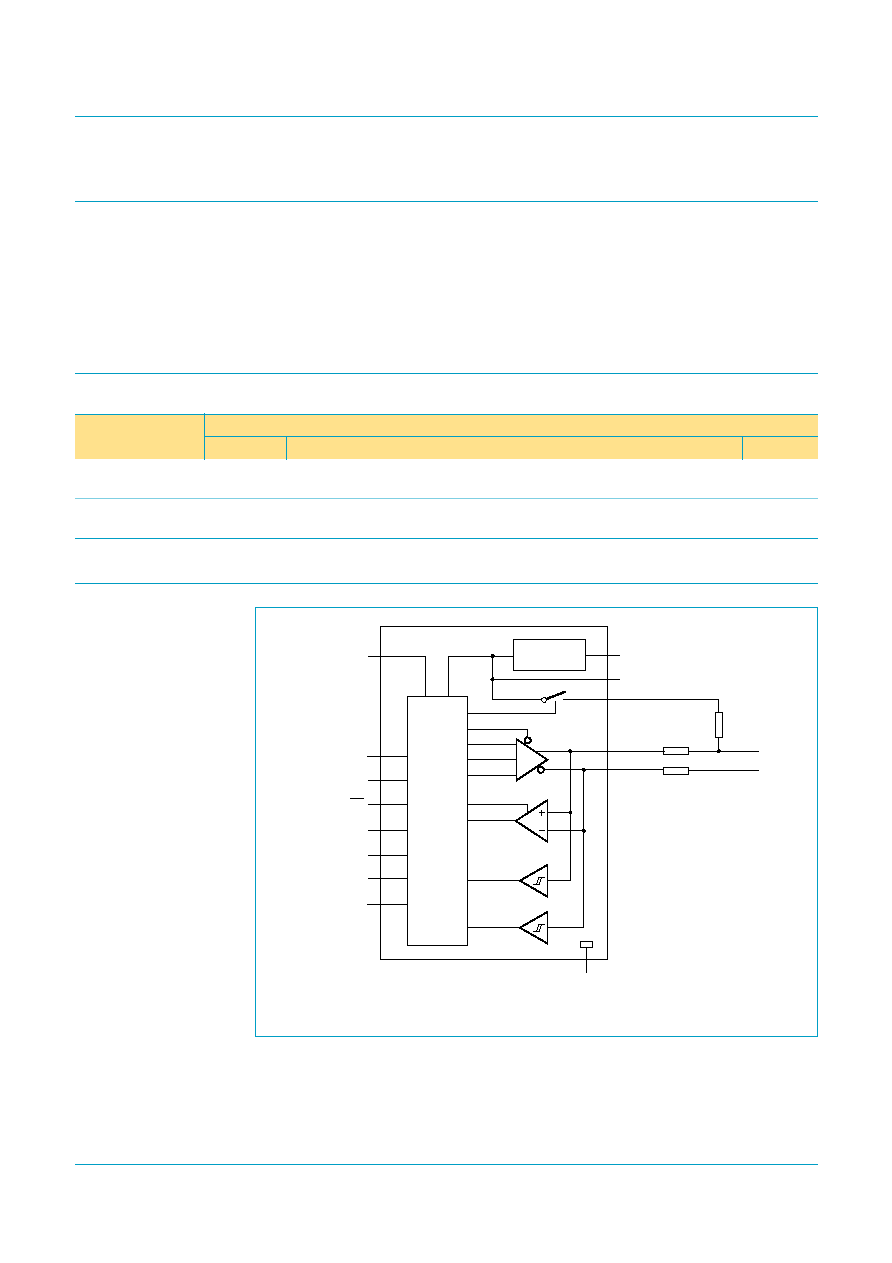
Block diagram
Table 1:
Ordering information
Type number
Package
Name
Description
Version
ISP1102W
HBCC16
plastic thermal enhanced bottom chip carrier; 16 terminals;
body 3
×
3
×
0.65 mm
SOT639-2
ISP1102BS
HVQFN14
plastic thermal enhanced very thin quad flat package; no leads;
14 terminals; body 2.5
×
2.5
×
0.85 mm
SOT773-1
Fig 1.
Block diagram.
004aaa207
VCC(I/O)
VCC(5.0)
VOLTAGE
REGULATOR
3.3 V
1.5 k
33
(1%)
33
(1%)
LEVEL
SHIFTER
ISP1102
SOFTCON
Vreg(3.3)
GND
Vpu(3.3)
D
+
D
-
OE
RCV
VP/VPO
VM/VMO
VBUSDET
SUSPND
Philips Semiconductors
ISP1102
Advanced USB transceiver
Product data
Rev. 03 -- 02 September 2003
3 of 23
9397 750 11228
© Koninklijke Philips Electronics N.V. 2003. All rights reserved.
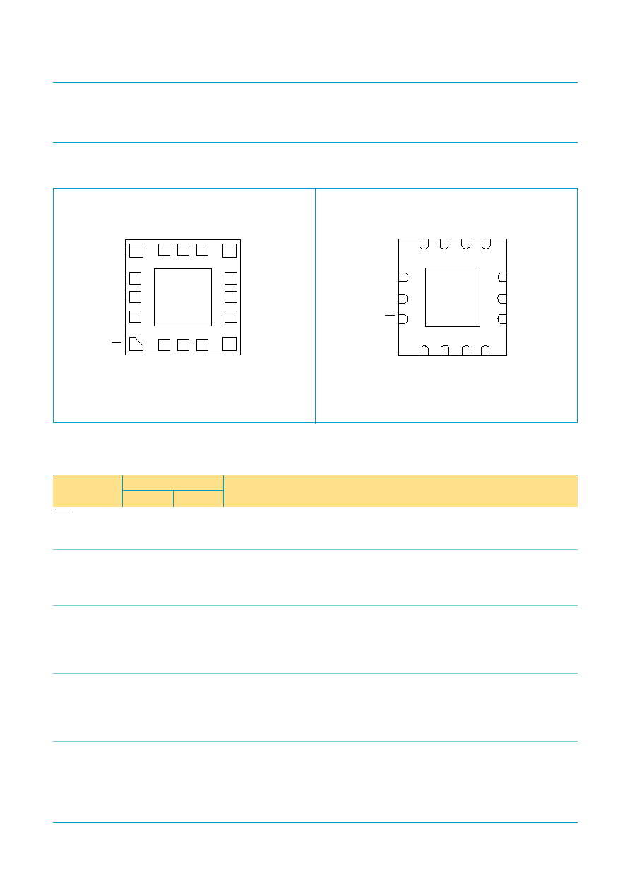
6.
Pinning information
6.1 Pinning
6.2 Pin description
Fig 2.
Pin configuration HBCC16.
Fig 3.
Pin configuration HVQFN14.
004aaa209
Bottom view
ISP1102W
SOFTCON
V
pu(3.3)
RCV
VP/VPO
OE
D
+
D
-
V
CC(I/O)
n.c.
VM/VMO
SUSPND
n.c.
V
CC(5.0)
Vreg(3.3)
n.c.
13
14
15
16
8
7
6
12
11
10
9
2
1
3
4
5
GND
(exposed diepad)
VBUSDET
004aaa208
Bottom view
ISP1102BS
SOFTCON
V
pu(3.3)
RCV
VP/VPO
OE
D
+
D
-
V
CC(I/O)
VM/VMO
SUSPND
V
CC(5.0)
V
reg(3.3)
7
GND
(exposed diepad)
VBUSDET
n.c.
4
5
6
3
2
1
8
9
10
11
12
13
14
Table 2:
Pin description
Symbol
[1]
Pin
Type
Description
HBCC16
HVQFN14
OE
1
1
I
input for output enable (CMOS level with respect to V
CC(I/O)
, active LOW);
enables the transceiver to transmit data on the USB bus
input pad; push pull; CMOS
RCV
2
2
O
differential data receiver output (CMOS level with respect to V
CC(I/O)
);
driven LOW when input SUSPND is HIGH; the output state of RCV is
preserved and stable during an SE0 condition
output pad; push pull; 4 mA output drive; CMOS
VP/VPO
3
3
I/O
single-ended D+ receiver output VP (CMOS level with respect to V
CC(I/O)
);
for external detection of SE0, error conditions, speed of connected device;
this pin also acts as the drive data input VPO; see
Table 3
and
Table 4
bidirectional pad; push-pull input; three-state output; 4 mA output drive;
CMOS
VM/VMO
4
4
I/O
single-ended D
-
receiver output VM (CMOS level with respect to V
CC(I/O)
);
for external detection of SE0, error conditions, speed of connected device;
this pin also acts as the drive data input VMO; see
Table 3
and
Table 4
bidirectional pad; push-pull input; three-state output; 4 mA output drive;
CMOS
SUSPND
5
5
I
suspend input (CMOS level with respect to V
CC(I/O)
); a HIGH level enables
low-power state while the USB bus is inactive and drives output RCV to a
LOW level
input pad; push pull; CMOS

Philips Semiconductors
ISP1102
Advanced USB transceiver
Product data
Rev. 03 -- 02 September 2003
4 of 23
9397 750 11228
© Koninklijke Philips Electronics N.V. 2003. All rights reserved.
[1]
Symbol names with an overscore (e.g. OE) indicate active LOW signals.
n.c.
6
-
-
not connected
V
CC(I/O)
7
6
-
supply voltage for digital I/O pins (1.65 to 3.6 V). When V
CC(I/O)
is not
connected, the D+ and D
-
pins are in three-state. This supply pin is totally
independent of V
CC(5.0)
and V
reg(3.3)
and must never exceed the V
reg(3.3)
voltage.
VBUSDET
8
7
O
V
BUS
indicator output (CMOS level with respect to V
CC(I/O)
); when
V
BUS
> 4.1 V, then VBUSDET = HIGH and when V
BUS
< 3.6 V, then
VBUSDET = LOW; when SUSPND = HIGH, then pin VBUSDET is pulled
HIGH
output pad; push pull; 4 mA output drive; CMOS
D
-
9
8
AI/O
negative USB data bus connection (analog, differential)
D+
10
9
AI/O
positive USB data bus connection (analog, differential)
n.c.
11
-
not connected
n.c.
12
-
not connected
n.c.
-
10
-
not connected
V
reg(3.3)
13
11
-
internal regulator option: regulated supply voltage output (3.0 to 3.6 V)
during 5 V operation; a decoupling capacitor of at least 0.1
µ
F is required
regulator bypass option: used as a supply voltage input (3.3 V
±
10%)
for 3.3 V operation
V
CC(5.0)
14
12
-
internal regulator option: supply voltage input (4.0 to 5.5 V); can be
connected directly to USB line V
BUS
regulator bypass option: connect to V
reg(3.3)
V
pu(3.3)
15
13
-
pull-up supply voltage (3.3 V
±
10%); connect an external 1.5 k
resistor
on D+ (full-speed).
Pin function is controlled by input SOFTCON:
SOFTCON = LOW -- V
pu(3.3)
floating (high impedance); ensures zero
pull-up current
SOFTCON = HIGH -- V
pu(3.3)
= 3.3 V; internally connected to V
reg(3.3)
SOFTCON
16
14
I
software controlled USB connection input; a HIGH level applies 3.3 V to
pin V
pu(3.3)
, which is connected to an external 1.5 k
pull-up resistor; this
allows USB connect or disconnect signalling to be controlled by software
input pad; push pull; CMOS
GND
exposed
die pad
exposed
die pad
-
ground supply; down bonded to the exposed die pad (heatsink); to be
connected to the PCB ground
Table 2:
Pin description
...continued
Symbol
[1]
Pin
Type
Description
HBCC16
HVQFN14

Philips Semiconductors
ISP1102
Advanced USB transceiver
Product data
Rev. 03 -- 02 September 2003
5 of 23
9397 750 11228
© Koninklijke Philips Electronics N.V. 2003. All rights reserved.
7.
Functional description
7.1 Function selection
[1]
Signal levels on the D+ and D
-
pins are determined by other USB devices and external pull-up or
pull-down resistors.
[2]
In the suspend mode (SUSPND = HIGH), the differential receiver is inactive and the output RCV is
always LOW. Out-of-suspend (K) signalling is detected via the single-ended receivers VP/VPO and
VM/VMO.
7.2 Operating functions
[1]
RCV* denotes the signal level on output RCV just before the SE0 state occurs. This level is stable
during the SE0 period.
7.3 Power supply configurations
The ISP1102 can be used with different power supply configurations, which can be
changed dynamically.
Table 7
provides an overview of the power supply
configurations.
Normal mode -- V
CC(I/O)
is connected. V
CC(5.0)
is connected only, or V
CC(5.0)
and
V
reg(3.3)
are connected.
For 5 V operation, V
CC(5.0)
is connected to a 5 V source (4.0 to 5.5 V). The internal
voltage regulator then produces 3.3 V for the USB connections.
Table 3:
Function table
SUSPND OE
D+, D
-
RCV
VP/VPO
VM/VMO
Function
L
L
driving/
receiving
active
VPO input
VMO input normal driving
(differential receiver
active)
L
H
receiving
[1]
active
VP output
VM output
receiving
H
L
driving
inactive
[2]
VPO input
VMO input driving during suspend
(differential receiver
inactive)
H
H
high-Z
[1]
inactive
[2]
VP output
VM output
low-power state
Table 4:
Driving function using differential input data interface (pin OE = L)
VM/VMO
VP/VPO
Data
L
L
SE0
L
H
differential logic 1
H
L
differential logic 0
H
H
illegal state
Table 5:
Receiving function (pin OE = H)
D+, D
-
RCV
VP/VPO
VM/VMO
differential logic 0
L
L
H
differential logic 1
H
H
L
SE0
RCV*
[1]
L
L

Philips Semiconductors
ISP1102
Advanced USB transceiver
Product data
Rev. 03 -- 02 September 2003
6 of 23
9397 750 11228
© Koninklijke Philips Electronics N.V. 2003. All rights reserved.
For 3.3 V operation, both V
CC(5.0)
and V
reg(3.3)
are connected to a 3.3 V source
(3.0 to 3.6 V).
V
CC(I/O)
is independently connected to a voltage source (1.65 to 3.6 V), depending on
the supply voltage of the external circuit.
Sharing mode -- V
CC(I/O)
is connected only; V
CC(5.0)
and V
reg(3.3)
are not connected.
In this mode, the D+ and D
-
pins are made three-state and the ISP1102 allows
external signals of up to 3.6 V to share the D+ and D
-
lines. The internal circuits of
the ISP1102 ensure that virtually no current (maximum 10
µ
A) is drawn via the
D+ and D
-
lines. The power consumption through pin V
CC(I/O)
drops to the low-power
(suspended) state level.
Pins VBUSDET and RCV are driven LOW to indicate this mode. The VBUSDET
function is ignored during the suspend mode of the ISP1102.
Some hysteresis is built into the detection of V
reg(3.3)
lost.
[1]
VP/VPO and VM/VMO are bidirectional pins.
Table 6:
Pin states in the sharing mode
Pin
Sharing mode
V
CC(5.0)
not present
V
reg(3.3)
not present
V
CC(I/O)
1.65 to 3.6 V input
V
pu(3.3)
high impedance (off)
D+, D
-
high impedance
VP/VPO, VM/VMO
[1]
L
RCV
L
VBUSDET
L
OE, SUSPND, SOFTCON
high impedance
Table 7:
Power supply configuration overview
V
CC(5.0)
Configuration
Special characteristics
connected
normal mode
-
not connected
sharing mode
D+, D
-
and V
pu(3.3)
high impedance;
VBUSDET driven LOW

Philips Semiconductors
ISP1102
Advanced USB transceiver
Product data
Rev. 03 -- 02 September 2003
7 of 23
9397 750 11228
© Koninklijke Philips Electronics N.V. 2003. All rights reserved.
7.4 Power supply input options
The ISP1102 has two power supply input options.
Internal regulator -- pin V
CC(5.0)
is connected to 4.0 to 5.5 V. The internal regulator
is used to supply the internal circuitry with 3.3 V (nominal). The V
reg(3.3)
pin becomes
a 3.3 V output reference.
Regulator bypass -- pins V
CC(5.0)
and V
reg(3.3)
are connected to the same supply.
The internal regulator is bypassed and the internal circuitry is supplied directly from
pin V
reg(3.3)
. The voltage range is 3.0 to 3.6 V to comply with the USB specification.
The supply voltage range for each input option is specified in
Table 8
.
Table 8:
Power supply input options
Input option V
CC(5.0)
V
reg(3.3)
V
CC(I/O)
Internal
regulator
supply input for internal
regulator (4.0 to 5.5 V)
voltage reference output
(3.3 V, 300
µ
A)
supply input for digital
I/O pins (1.65 V to 3.6 V)
Regulator
bypass
connected to V
reg(3.3)
with maximum voltage
drop of 0.3 V
(2.7 to 3.6 V)
supply input
(3.0 V to 3.6 V)
supply input for digital
I/O pins (1.65 V to 3.6 V)
Philips Semiconductors
ISP1102
Advanced USB transceiver
Product data
Rev. 03 -- 02 September 2003
8 of 23
9397 750 11228
© Koninklijke Philips Electronics N.V. 2003. All rights reserved.
8.
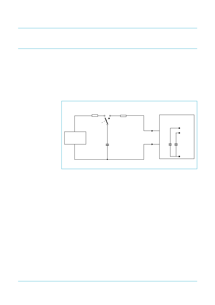
Electrostatic discharge (ESD)
8.1 ESD protection
For HBCC package, the pins that are connected to the USB connector (D+, D
-
,
V
CC(5.0)
and GND) have a minimum of
±
12 kV ESD protection. The
±
12 kV
measurement is limited by the test equipment. Capacitors of 4.7
µ
F connected from
V
reg(3.3)
to GND and V
CC(5.0)
to GND are required to achieve this
±
12 kV ESD
protection (see
Figure 4
).
The ISP1102W can withstand
±
12 kV using the Human Body Model and
±
5 kV using
the Contact Discharge Method as specified in
IEC 61000-4-2.
Note: For HVQFN package, the pins that are connected to the USB connector (D+,
D
-
, V
CC(5.0)
and GND) have a minimum of
±
7 kV ESD protection.
8.2 ESD test conditions
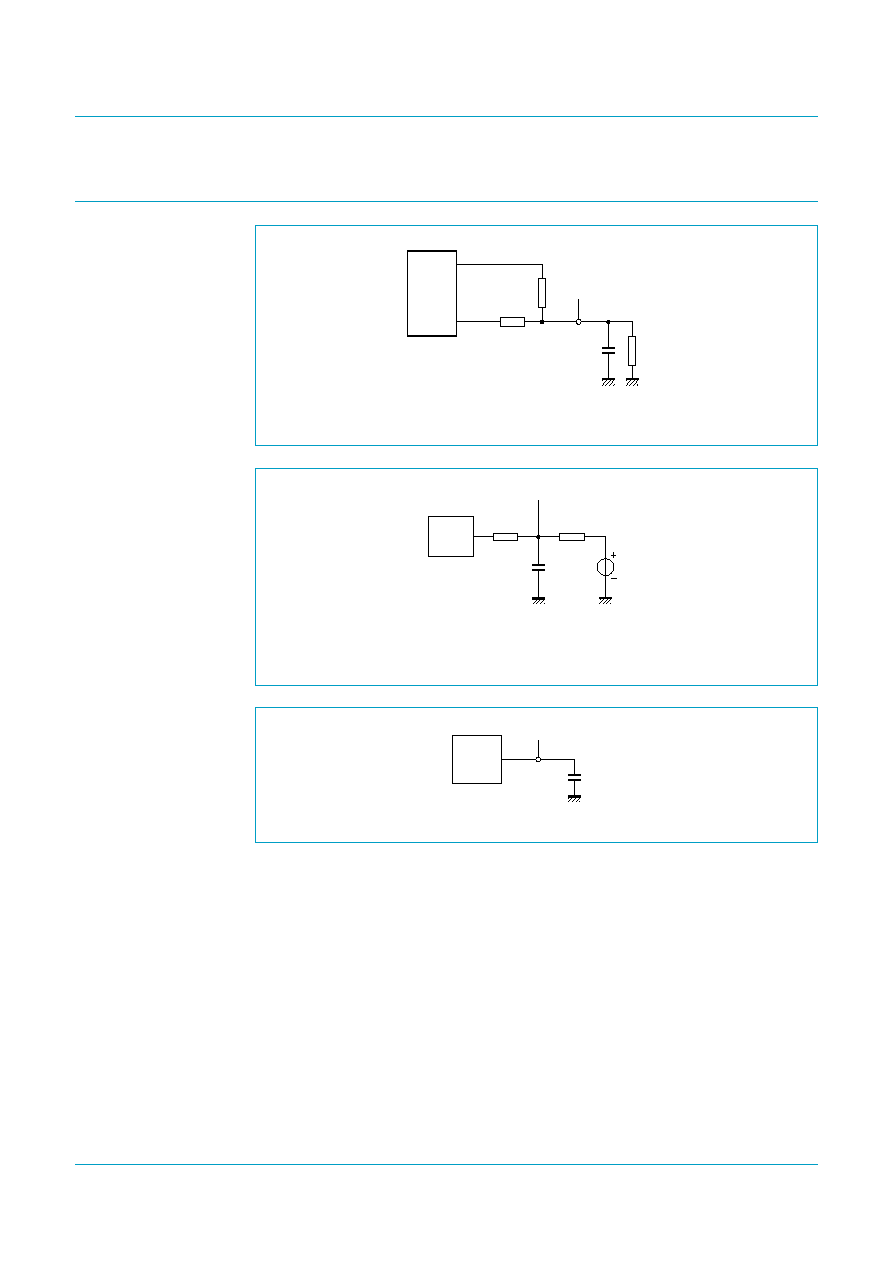
A detailed report on test set-up and results is available on request.
Fig 4.
Human Body ESD test model.
1 M
1500
HIGH VOLTAGE
DC SOURCE
4.7
µ
F
4.7
µ
F
R
C
R
D
V
CC(5.0)
V
reg(3.3)
DEVICE UNDER
TEST
C
S
100 pF
storage
capacitor
charge current
limit resistor
discharge
resistance
GND
A
B
004aaa145

Philips Semiconductors
ISP1102
Advanced USB transceiver
Product data
Rev. 03 -- 02 September 2003
9 of 23
9397 750 11228
© Koninklijke Philips Electronics N.V. 2003. All rights reserved.
9.
Limiting values
[1]
Testing equipment limits measurement to only
±
12 kV. Capacitors needed on V
CC(5.0)
and V
reg(3.3)
(see
Section 8
).
[2]
Equivalent to discharging a 100 pF capacitor via a 1.5 k
resistor (Human Body Model).
10. Recommended operating conditions
11. Static characteristics
Table 9:
Absolute maximum ratings
In accordance with the Absolute Maximum Rating System (IEC 60134).
Symbol
Parameter
Conditions
Min
Max
Unit
V
CC(5.0)
supply voltage
-
0.5
+6.0
V
V
CC(I/O)
I/O supply voltage
-
0.5
+4.6
V
V
I
DC input voltage
-
0.5
V
CC(I/O)
+ 0.5 V
I
lu
latch-up current
V
I
=
-
1.8 to +5.4 V
-
100
mA
V
esd
electrostatic discharge voltage
pins D+, D
-
, V
CC(5.0)
and
GND; I
LI
< 3
µ
A for HBCC
package
[1][2]
-
12000
+12000
V
pins D+, D
-
, V
CC(5.0)
and
GND; I
LI
< 3
µ
A for HVQFN
package
[2]
-
7000
+7000
V
all other pins; I
LI
< 1
µ
A
[2]
-
2000
+2000
V
T
stg
storage temperature
-
40
+125
°
C
Table 10:
Recommended operating conditions
Symbol
Parameter
Conditions
Min
Typ
Max
Unit
V
CC(5.0)
supply voltage
4.0
5.0
5.5
V
V
CC(I/O)
I/O supply voltage
1.65
-
3.6
V
V
I
input voltage
0
-
V
CC(I/O)
V
V
I(AI/O)
input voltage on AI/O pins
pins D+ and D
-
0
-
3.6
V
T
amb
ambient temperature
-
40
-
+85
°
C
Table 11:
Static characteristics: supply pins
V
CC(5.0)
= 4.0 to 5.5 V or V
reg(3.3)
= 3.0 to 3.6 V; V
CC(I/O)
= 1.65 to 3.6 V; V
GND
= 0 V; see
Table 8
for valid voltage level
combinations; T
amb
=
-
40 to +85
°
C; unless otherwise specified.
Symbol
Parameter
Conditions
Min
Typ
Max
Unit
V
reg(3.3)
regulated supply voltage output
internal regulator option;
I
load
300
µ
A
[1][2]
3.0
3.3
3.6
V
I
CC
operating supply current
transmitting and receiving at
12 Mbit/s; C
L
= 50 pF on
pins D+ and D
-
[3]
-
4
8
mA
I
CC(I/O)
operating I/O supply current
transmitting and receiving at
12 Mbit/s
[3]
-
1
2
mA
I
CC(idle)
supply current during full-speed
idle and SE0
idle: V
D+
> 2.7 V, V
D
-
< 0.3 V;
SE0: V
D+
< 0.3 V, V
D
-
< 0.3 V
[4]
-
-
300
µ
A
I
CC(I/O)(static)
static I/O supply current
idle, SE0 or suspend
-
-
20
µ
A

Philips Semiconductors
ISP1102
Advanced USB transceiver
Product data
Rev. 03 -- 02 September 2003
10 of 23
9397 750 11228
© Koninklijke Philips Electronics N.V. 2003. All rights reserved.
[1]
I
load
includes the pull-up resistor current via pin V
pu(3.3)
.
[2]
The minimum voltage is 2.7 V in the suspend mode.
[3]
Maximum value characterized only, not tested in production.
[4]
Excluding any load current and V
pu(3.3)
or V
sw
source current to the 1.5 k
and 15 k
pull-up and pull-down resistors (200
µ
A typ.).
[5]
When V
CC(I/O)
< 2.7 V, the minimum value for V
reg(3.3)th
= 2.0 V for supply present condition.
I
CC(susp)
suspend supply current
SUSPND = HIGH
[4]
-
-
20
µ
A
I
CC(I/O)(sharing)
sharing mode I/O supply current V
CC(5.0)
not connected
-
-
20
µ
A
I
Dx(sharing)
sharing mode load current on
pins D+ and D
-
V
CC(5.0)
not connected;
SOFTCON = LOW;
V
Dx
= 3.6 V
-
-
10
µ
A
V
CC(5.0)th
supply voltage detection
threshold
1.65 V
V
CC(I/O)
3.6 V
supply lost
-
-
3.6
V
supply present
4.1
-
-
V
V
CC(5.0)hys
supply voltage detection
hysteresis
V
CC(I/O)
= 1.8 V
-
70
-
mV
V
CC(I/O)th
I/O supply voltage detection
threshold
V
reg(3.3)
= 2.7 to 3.6 V
supply lost
-
-
0.5
V
supply present
1.4
-
-
V
V
CC(I/O)hys
I/O supply voltage detection
hysteresis
V
reg(3.3)
= 3.3 V
-
0.45
-
V
V
reg(3.3)th
regulated supply voltage
detection threshold
1.65 V
V
CC(I/O)
V
reg(3.3)
;
2.7 V
V
reg(3.3)
3.6 V
supply lost
-
-
0.8
V
supply present
[5]
2.4
-
-
V
V
reg(3.3)hys
regulated supply voltage
detection hysteresis
V
CC(I/O)
= 1.8 V
-
0.45
-
V
Table 11:
Static characteristics: supply pins
...continued
V
CC(5.0)
= 4.0 to 5.5 V or V
reg(3.3)
= 3.0 to 3.6 V; V
CC(I/O)
= 1.65 to 3.6 V; V
GND
= 0 V; see
Table 8
for valid voltage level
combinations; T
amb
=
-
40 to +85
°
C; unless otherwise specified.
Symbol
Parameter
Conditions
Min
Typ
Max
Unit
Table 12:
Static characteristics: digital pins
V
CC(I/O)
= 1.65 to 3.6 V; V
GND
= 0 V; T
amb
=
-
40 to +85
°
C; unless otherwise specified.
Symbol
Parameter
Conditions
Min
Typ
Max
Unit
V
CC(I/O)
= 1.65 to 3.6 V
Input levels
V
IL
LOW-level input voltage
-
-
0.3V
CC(I/O)
V
V
IH
HIGH-level input voltage
0.6V
CC(I/O)
-
-
V
Output levels
V
OL
LOW-level output voltage
I
OL
= 100
µ
A
-
-
0.15
V
I
OL
= 2 mA
-
-
0.4
V
V
OH
HIGH-level output voltage
I
OH
= 100
µ
A
V
CC(I/O)
-
0.15
-
-
V
I
OH
= 2 mA
V
CC(I/O)
-
0.4
-
-
V
Leakage current
I
LI
input leakage current
[1]
-
1
-
+1
µ
A

Philips Semiconductors
ISP1102
Advanced USB transceiver
Product data
Rev. 03 -- 02 September 2003
11 of 23
9397 750 11228
© Koninklijke Philips Electronics N.V. 2003. All rights reserved.
[1]
If V
CC(I/O)
V
reg(3.3)
, then the leakage current will be higher than the specified value.
Capacitance
C
IN
input capacitance
pin to GND
-
-
10
pF
Example 1: V
CC(I/O)
= 1.8 V
±
0.15 V
Input levels
V
IL
LOW-level input voltage
-
-
0.5
V
V
IH
HIGH-level input voltage
1.2
-
-
V
Output levels
V
OL
LOW-level output voltage
I
OL
= 100
µ
A
-
-
0.15
V
I
OL
= 2 mA
-
-
0.4
V
V
OH
HIGH-level output voltage
I
OH
= 100
µ
A
1.5
-
-
V
I
OH
= 2 mA
1.25
-
-
V
Example 2: V
CC(I/O)
= 2.5 V
±
0.2 V
Input levels
V
IL
LOW-level input voltage
-
-
0.7
V
V
IH
HIGH-level input voltage
1.7
-
-
V
Output levels
V
OL
LOW-level output voltage
I
OL
= 100
µ
A
-
-
0.15
V
I
OL
= 2 mA
-
-
0.4
V
V
OH
HIGH-level output voltage
I
OH
= 100
µ
A
2.15
-
-
V
I
OH
= 2 mA
1.9
-
-
V
Example 3: V
CC(I/O)
= 3.3 V
±
0.3 V
Input levels
V
IL
LOW-level input voltage
-
-
0.9
V
V
IH
HIGH-level input voltage
2.15
-
-
V
Output levels
V
OL
LOW-level output voltage
I
OL
= 100
µ
A
-
-
0.15
V
I
OL
= 2 mA
-
-
0.4
V
V
OH
HIGH-level output voltage
I
OH
= 100
µ
A
2.85
-
-
V
I
OH
= 2 mA
2.6
-
-
V
Table 12:
Static characteristics: digital pins
...continued
V
CC(I/O)
= 1.65 to 3.6 V; V
GND
= 0 V; T
amb
=
-
40 to +85
°
C; unless otherwise specified.
Symbol
Parameter
Conditions
Min
Typ
Max
Unit
Table 13:
Static characteristics: analog I/O pins D+ and D
-
V
CC(5.0)
= 4.0 to 5.5 V or V
reg(3.3)
= 3.0 to 3.6 V; V
GND
= 0 V; T
amb
=
-
40 to +85
°
C; unless otherwise specified.
Symbol
Parameter
Conditions
Min
Typ
Max
Unit
Input levels
Differential receiver
V
DI
differential input sensitivity
|
V
I(D+)
-
V
I(D
-
)
|
0.2
-
-
V
V
CM
differential common mode
voltage
includes V
DI
range
0.8
-
2.5
V

Philips Semiconductors
ISP1102
Advanced USB transceiver
Product data
Rev. 03 -- 02 September 2003
12 of 23
9397 750 11228
© Koninklijke Philips Electronics N.V. 2003. All rights reserved.
[1]
V
OH(min)
= V
reg(3.3)
-
0.2 V.
[2]
Includes external resistors of 33
±
1% on both pins D+ and D
-
.
[3]
This voltage is available at pins V
reg(3.3)
and V
pu(3.3)
.
[4]
The minimum voltage is 2.7 V in the suspend mode.
12. Dynamic characteristics
Single-ended receiver
V
IL
LOW-level input voltage
-
-
0.8
V
V
IH
HIGH-level input voltage
2.0
-
-
V
V
hys
hysteresis voltage
0.4
-
0.7
V
Output levels
V
OL
LOW-level output voltage
R
L
= 1.5 k
to 3.6 V
-
-
0.3
V
V
OH
HIGH-level output voltage
R
L
= 15 k
to GND
[1]
2.8
-
3.6
V
Leakage current
I
LZ
OFF-state leakage current
-
1
-
+1
µ
A
Capacitance
C
IN
transceiver capacitance
pin to GND
-
-
20
pF
Resistance
Z
DRV
driver output impedance
steady-state drive
[2]
34
39
44
Z
INP
input impedance
10
-
-
M
R
SW
internal switch resistance at
pin V
pu(3.3)
-
-
10
Termination
V
TERM
termination voltage for
upstream port pull-up (R
pu
)
[3][4]
3.0
-
3.6
V
Table 13:
Static characteristics: analog I/O pins D+ and D
-
...continued
V
CC(5.0)
= 4.0 to 5.5 V or V
reg(3.3)
= 3.0 to 3.6 V; V
GND
= 0 V; T
amb
=
-
40 to +85
°
C; unless otherwise specified.
Symbol
Parameter
Conditions
Min
Typ
Max
Unit
Table 14:
Dynamic characteristics: analog I/O pins D+ and D
-
V
CC(5.0)
= 4.0 to 5.5 V or V
reg(3.3)
= 3.0 to 3.6 V; V
CC(I/O)
= 1.65 to 3.6 V; V
GND
= 0 V; see
Table 8
for valid voltage level
combinations; T
amb
=
-
40 to +85
°
C; unless otherwise specified.
Symbol
Parameter
Conditions
Min
Typ
Max
Unit
Driver characteristics
t
FR
rise time
C
L
= 50 to 125 pF;
10% to 90% of
|
V
OH
-
V
OL
|
;
see
Figure 5
4
-
20
ns
t
FF
fall time
C
L
= 50 to 125 pF;
90% to 10% of
|
V
OH
-
V
OL
|
;
see
Figure 5
4
-
20
ns
FRFM
differential rise/fall time
matching (t
FR
/t
FF
)
excluding the first transition
from Idle state
90
-
111.1
%
V
CRS
output signal crossover
voltage
excluding the first transition
from Idle state; see
Figure 6
[1]
1.3
-
2.0
V

Philips Semiconductors
ISP1102
Advanced USB transceiver
Product data
Rev. 03 -- 02 September 2003
13 of 23
9397 750 11228
© Koninklijke Philips Electronics N.V. 2003. All rights reserved.
[1]
Characterized only, not tested. Limits guaranteed by design.
Driver timing
t
PLH(drv)
driver propagation delay
(VPO, VMO to D+, D
-
)
LOW-to-HIGH; see
Figure 6
and
Figure 9
-
-
18
ns
t
PHL(drv)
driver propagation delay
(VPO, VMO to D+, D
-
)
HIGH-to-LOW; see
Figure 6
and
Figure 9
-
-
18
ns
t
PHZ
driver disable delay
(OE to D+, D
-
)
HIGH-to-OFF; see
Figure 7
and
Figure 10
-
-
15
ns
t
PLZ
driver disable delay
(OE to D+, D
-
)
LOW-to-OFF; see
Figure 7
and
Figure 10
-
-
15
ns
t
PZH
driver enable delay
(OE to D+, D
-
)
OFF-to-HIGH; see
Figure 7
and
Figure 10
-
-
15
ns
t
PZL
driver enable delay
(OE to D+, D
-
)
OFF-to-LOW; see
Figure 7
and
Figure 10
-
-
15
ns
Receiver timings
Differential receiver
t
PLH(rcv)
propagation delay
(D+, D
-
to RCV)
LOW-to-HIGH; see
Figure 8
and
Figure 11
-
-
15
ns
t
PHL(rcv)
propagation delay
(D+, D
-
to RCV)
HIGH-to-LOW; see
Figure 8
and
Figure 11
-
-
15
ns
Single-ended receiver
t
PLH(se)
propagation delay
(D+, D
-
to VP/VPO,
VM/VMO)
LOW-to-HIGH; see
Figure 8
and
Figure 11
-
-
18
ns
t
PHL(se)
propagation delay
(D+, D
-
to VP/VPO,
VM/VMO)
HIGH-to-LOW; see
Figure 8
and
Figure 11
-
-
18
ns
Table 14:
Dynamic characteristics: analog I/O pins D+ and D
-
...continued
V
CC(5.0)
= 4.0 to 5.5 V or V
reg(3.3)
= 3.0 to 3.6 V; V
CC(I/O)
= 1.65 to 3.6 V; V
GND
= 0 V; see
Table 8
for valid voltage level
combinations; T
amb
=
-
40 to +85
°
C; unless otherwise specified.
Symbol
Parameter
Conditions
Min
Typ
Max
Unit
Philips Semiconductors
ISP1102
Advanced USB transceiver
Product data
Rev. 03 -- 02 September 2003
14 of 23
9397 750 11228
© Koninklijke Philips Electronics N.V. 2003. All rights reserved.
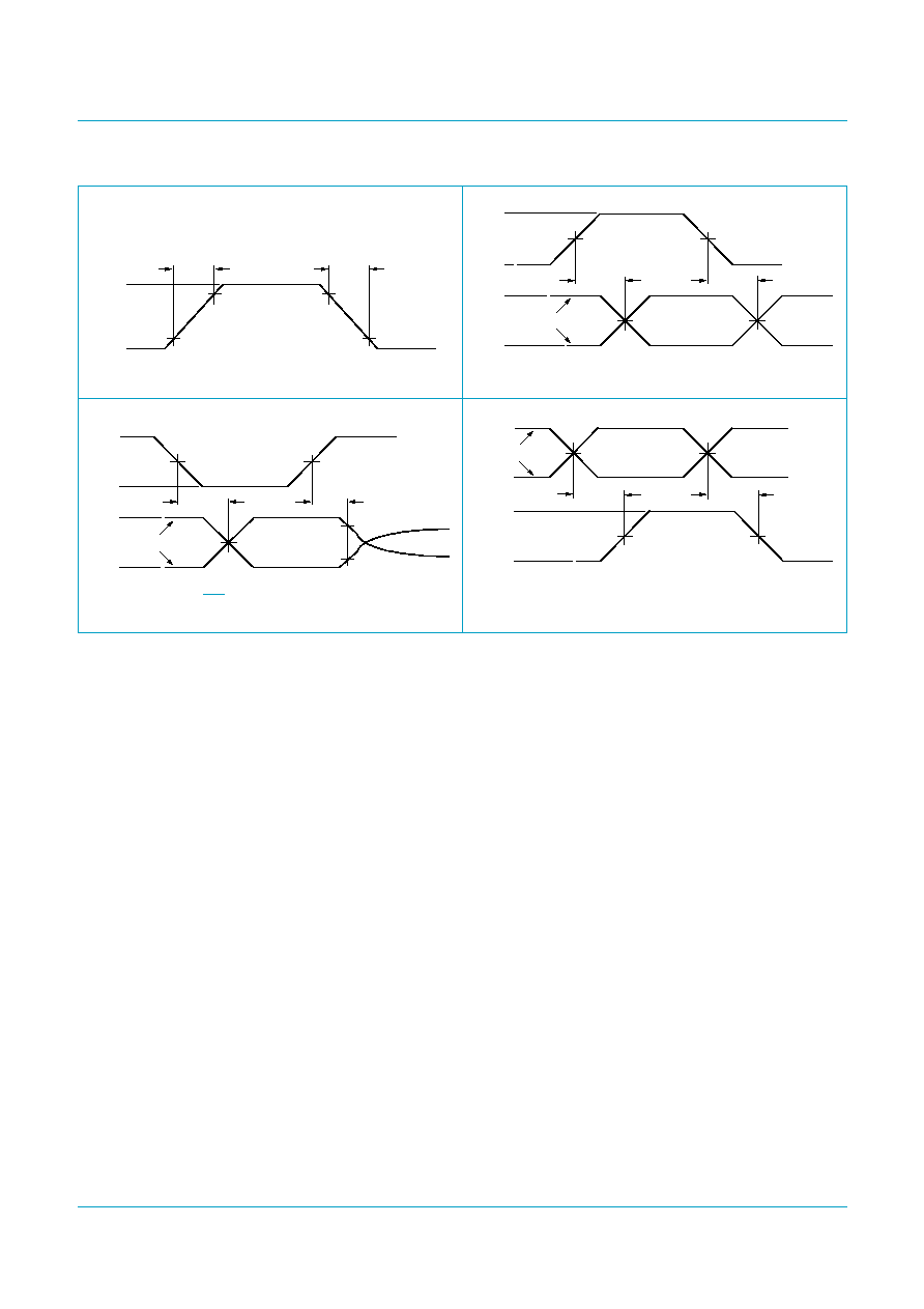
Fig 5.
Rise and fall times.
Fig 6.
Timing of VPO and VMO to D+ and D
-.
Fig 7.
Timing of OE to D+ and D
-
.
Fig 8.
Timing of D+ and D
-
to RCV, VP/VPO and
VM/VMO.
MGS963
VOL
tFR, tLR
tFF, tLF
VOH
90 %
10 %
10 %
90 %
MGS964
VOL
VOH
tPHL(drv)
tPLH(drv)
VCRS
VCRS
0.9 V
0.9 V
1.65 V
0 V
logic input
differential
data lines
MGS966
VOL
VOH
tPZH
tPZL
tPHZ
tPLZ
VOH
-
0.3 V
VOL
+
0.3 V
VCRS
0.9 V
0.9 V
1.65 V
0 V
logic input
differential
data lines
MGS965
VOL
VOH
tPHL(rcv)
tPHL(se)
tPLH(rcv)
tPLH(se)
VCRS
VCRS
0.9 V
0.9 V
2.0 V
0.8 V
logic output
differential
data lines
Philips Semiconductors
ISP1102
Advanced USB transceiver
Product data
Rev. 03 -- 02 September 2003
15 of 23
9397 750 11228
© Koninklijke Philips Electronics N.V. 2003. All rights reserved.
13. Test information
Load capacitance C
L
= 50 pF (minimum or maximum timing)
Fig 9.
Load on pins D+ and D
-
.
V = 0 V for t
PZH
and t
PHZ
V = V
reg(3.3)
for t
PZL
and t
PLZ
Fig 10. Load on pins D+ and D
-
for enable and disable times.
Fig 11. Load on pins VM/VMO, VP/VPO and RCV.
004aaa037
CL
test point
15 k
D
+
/D
-
Vpu(3.3)
1.5 k
33
D.U.T.
test point
V
33
D.U.T.
500
50 pF
MBL142
MGS968
25 pF
test point
D.U.T.
Philips Semiconductors
ISP1102
Advanced USB transceiver
Product data
Rev. 03 -- 02 September 2003
16 of 23
9397 750 11228
© Koninklijke Philips Electronics N.V. 2003. All rights reserved.
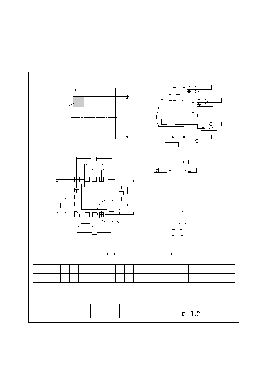
14. Package outline
Fig 12. Package outline HBCC16.
2.5
A
1
b
A
2
UNIT
D
Eh
e1
REFERENCES
OUTLINE
VERSION
EUROPEAN
PROJECTION
ISSUE DATE
01-11-13
03-03-12
IEC
JEDEC
JEITA
mm
0.8
0.10
0.05
0.7
0.6
3.1
2.9
1.45
1.35
3.1
2.9
1.45
1.35
0.33
0.27
DIMENSIONS (mm are the original dimensions)
SOT639-2
MO-217
Dh
0.33
0.27
b1
0.38
0.32
b3
0.38
0.32
b2
2.45
e3
E
0.23
0.17
f
0.5
w
e
y
y1
0.1
0.05
0.2
2.5
e2
2.45
e4
0.08
v
0
2.5
5 mm
scale
SOT639-2
HBCC16: plastic thermal enhanced bottom chip carrier; 16 terminals; body 3 x 3 x 0.65 mm
A
max.
detail X
y
y1 C
e
e
e1
e3
Dh
e4
D
E
X
C
B
A
16
1
13
5
9
e2
1/2 e3
1/2 e4
Eh
A1
A2
A
b2
b1
b3
b
f
terminal 1
index area
A
C
C
B
v
M
w
M
A
C
C
B
v
M
w
M
A
C
C
B
v
M
w
M
A
C
C
B
v
M
w
M
Philips Semiconductors
ISP1102
Advanced USB transceiver
Product data
Rev. 03 -- 02 September 2003
17 of 23
9397 750 11228
© Koninklijke Philips Electronics N.V. 2003. All rights reserved.
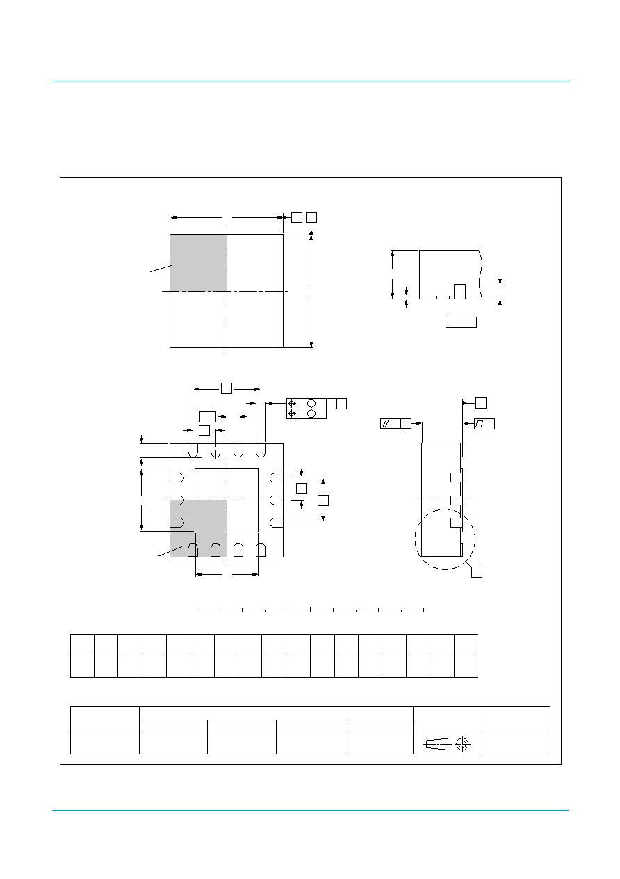
Fig 13. Package outline HVQFN14.
0.5
1
A1
Eh
b
UNIT
y
e
0.2
c
REFERENCES
OUTLINE
VERSION
EUROPEAN
PROJECTION
ISSUE DATE
IEC
JEDEC
JEITA
mm
2.6
2.4
Dh
1.45
1.15
y1
2.6
2.4
1.45
1.15
e1
1.5
e2
1
0.30
0.18
0.05
0.00
0.05
0.1
DIMENSIONS (mm are the original dimensions)
SOT773-1
- - -
- - -
- - -
0.35
0.25
L
0.1
v
0.05
w
0
2.5
5 mm
scale
SOT773-1
HVQFN14: plastic thermal enhanced very thin quad flat package; no leads;
14 terminals; body 2.5 x 2.5 x 0.85 mm
A
(1)
max.
A
A1
c
detail X
y
y1 C
X
D
E
C
B
A
02-07-05
terminal 1
index area
E
(1)
Note
1. Plastic or metal protrusions of 0.075 mm maximum per side are not included.
D
(1)
terminal 1
index area
e
L
Eh
Dh
e
e1
b
4
7
14
11
10
8
3
1
A
C
C
B
v
M
w
M
e2
1/2
e
Philips Semiconductors
ISP1102
Advanced USB transceiver
Product data
Rev. 03 -- 02 September 2003
18 of 23
9397 750 11228
© Koninklijke Philips Electronics N.V. 2003. All rights reserved.
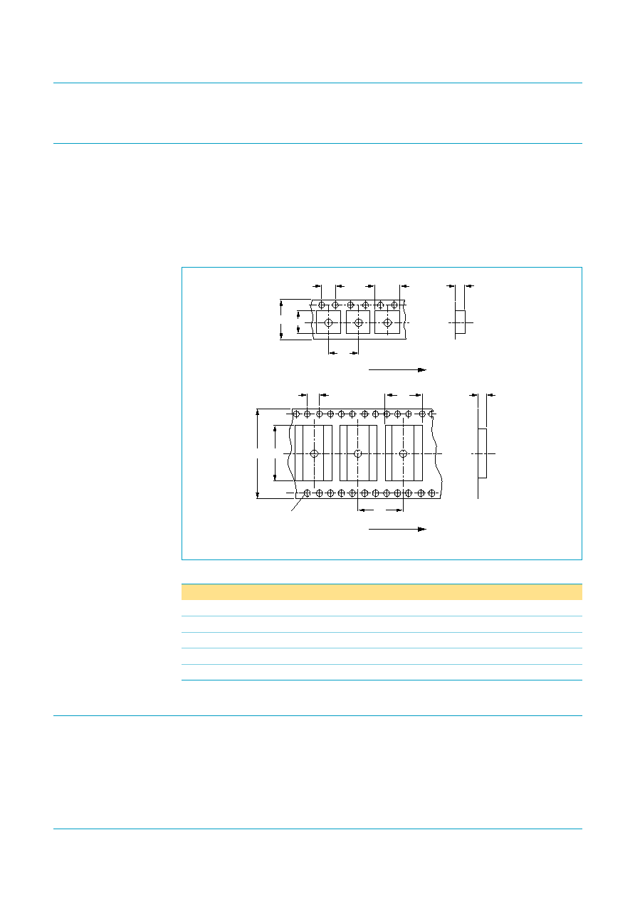
15. Packaging
The ISP1102W (HBCC16 package) is delivered on a Type A carrier tape, see
Figure 14
. The tape dimensions are given in
Table 15
.
The reel diameter is 330 mm. The reel is made of polystyrene (PS) and is not
designed for use in a baking process.
The cumulative tolerance of 10 successive sprocket holes is
±
0.02 mm. The camber
must not exceed 1 mm in 100 mm.
16. Soldering
16.1 Introduction to soldering surface mount packages
This text gives a very brief insight to a complex technology. A more in-depth account
of soldering ICs can be found in our
Data Handbook IC26; Integrated Circuit
Packages (document order number 9398 652 90011).
Fig 14. Carrier tape dimensions.
Table 15:
Type A carrier tape dimensions for the ISP1102W
Dimension
Value
Unit
A0
3.3
mm
B0
3.3
mm
K0
1.1
mm
P1
8.0
mm
W
12.0
±
0.3
mm
idth
MLC338
Type B
Type A
B0
4
W
K0
A0
4
K0
A0
P1
B0
P1
elongated
sprocket hole
direction of feed
W
direction of feed

Philips Semiconductors
ISP1102
Advanced USB transceiver
Product data
Rev. 03 -- 02 September 2003
19 of 23
9397 750 11228
© Koninklijke Philips Electronics N.V. 2003. All rights reserved.
There is no soldering method that is ideal for all IC packages. Wave soldering can still
be used for certain surface mount ICs, but it is not suitable for fine pitch SMDs. In
these situations reflow soldering is recommended. In these situations reflow
soldering is recommended.
16.2 Reflow soldering
Reflow soldering requires solder paste (a suspension of fine solder particles, flux and
binding agent) to be applied to the printed-circuit board by screen printing, stencilling
or pressure-syringe dispensing before package placement. Driven by legislation and
environmental forces the worldwide use of lead-free solder pastes is increasing.
Several methods exist for reflowing; for example, convection or convection/infrared
heating in a conveyor type oven. Throughput times (preheating, soldering and
cooling) vary between 100 and 200 seconds depending on heating method.
Typical reflow peak temperatures range from 215 to 270
°
C depending on solder
paste material. The top-surface temperature of the packages should preferably be
kept:
·
below 220
°
C (SnPb process) or below 245
°
C (Pb-free process)
for all BGA and SSOP-T packages
for packages with a thickness
2.5 mm
for packages with a thickness < 2.5 mm and a volume
350 mm
3
so called
thick/large packages.
·
below 235
°
C (SnPb process) or below 260
°
C (Pb-free process) for packages with
a thickness < 2.5 mm and a volume < 350 mm
3
so called small/thin packages.
Moisture sensitivity precautions, as indicated on packing, must be respected at all
times.
16.3 Wave soldering
Conventional single wave soldering is not recommended for surface mount devices
(SMDs) or printed-circuit boards with a high component density, as solder bridging
and non-wetting can present major problems.
To overcome these problems the double-wave soldering method was specifically
developed.
If wave soldering is used the following conditions must be observed for optimal
results:
·
Use a double-wave soldering method comprising a turbulent wave with high
upward pressure followed by a smooth laminar wave.
·
For packages with leads on two sides and a pitch (e):
larger than or equal to 1.27 mm, the footprint longitudinal axis is preferred to be
parallel to the transport direction of the printed-circuit board;
smaller than 1.27 mm, the footprint longitudinal axis must be parallel to the
transport direction of the printed-circuit board.
The footprint must incorporate solder thieves at the downstream end.

Philips Semiconductors
ISP1102
Advanced USB transceiver
Product data
Rev. 03 -- 02 September 2003
20 of 23
9397 750 11228
© Koninklijke Philips Electronics N.V. 2003. All rights reserved.
·
For packages with leads on four sides, the footprint must be placed at a 45
°
angle
to the transport direction of the printed-circuit board. The footprint must
incorporate solder thieves downstream and at the side corners.
During placement and before soldering, the package must be fixed with a droplet of
adhesive. The adhesive can be applied by screen printing, pin transfer or syringe
dispensing. The package can be soldered after the adhesive is cured.
Typical dwell time of the leads in the wave ranges from 3 to 4 seconds at 250
°
C or
265
°
C, depending on solder material applied, SnPb or Pb-free respectively.
A mildly-activated flux will eliminate the need for removal of corrosive residues in
most applications.
16.4 Manual soldering
Fix the component by first soldering two diagonally-opposite end leads. Use a low
voltage (24 V or less) soldering iron applied to the flat part of the lead. Contact time
must be limited to 10 seconds at up to 300
°
C.
When using a dedicated tool, all other leads can be soldered in one operation within
2 to 5 seconds between 270 and 320
°
C.
16.5 Package related soldering information
[1]
For more detailed information on the BGA packages refer to the
(LF)BGA Application Note
(AN01026); order a copy from your Philips Semiconductors sales office.
[2]
All surface mount (SMD) packages are moisture sensitive. Depending upon the moisture content, the
maximum temperature (with respect to time) and body size of the package, there is a risk that internal
or external package cracks may occur due to vaporization of the moisture in them (the so called
popcorn effect). For details, refer to the Drypack information in the
Data Handbook IC26; Integrated
Circuit Packages; Section: Packing Methods.
[3]
These transparent plastic packages are extremely sensitive to reflow soldering conditions and must
on no account be processed through more than one soldering cycle or subjected to infrared reflow
soldering with peak temperature exceeding 217
°
C
±
10
°
C measured in the atmosphere of the reflow
oven. The package body peak temperature must be kept as low as possible.
[4]
These packages are not suitable for wave soldering. On versions with the heatsink on the bottom
side, the solder cannot penetrate between the printed-circuit board and the heatsink. On versions with
the heatsink on the top side, the solder might be deposited on the heatsink surface.
Table 16:
Suitability of surface mount IC packages for wave and reflow soldering
methods
Package
[1]
Soldering method
Wave
Reflow
[2]
BGA, LBGA, LFBGA, SQFP, SSOP-T
[3]
,
TFBGA, VFBGA
not suitable
suitable
DHVQFN, HBCC, HBGA, HLQFP, HSQFP,
HSOP, HTQFP, HTSSOP, HVQFN, HVSON,
SMS
not suitable
[4]
suitable
PLCC
[5]
, SO, SOJ
suitable
suitable
LQFP, QFP, TQFP
not recommended
[5][6]
suitable
SSOP, TSSOP, VSO, VSSOP
not recommended
[7]
suitable
PMFP
[8]
not suitable
not suitable

Philips Semiconductors
ISP1102
Advanced USB transceiver
Product data
Rev. 03 -- 02 September 2003
21 of 23
9397 750 11228
© Koninklijke Philips Electronics N.V. 2003. All rights reserved.
[5]
If wave soldering is considered, then the package must be placed at a 45
°
angle to the solder wave
direction. The package footprint must incorporate solder thieves downstream and at the side corners.
[6]
Wave soldering is suitable for LQFP, QFP and TQFP packages with a pitch (e) larger than 0.8 mm; it
is definitely not suitable for packages with a pitch (e) equal to or smaller than 0.65 mm.
[7]
Wave soldering is suitable for SSOP and TSSOP packages with a pitch (e) equal to or larger than
0.65 mm; it is definitely not suitable for packages with a pitch (e) equal to or smaller than 0.5 mm.
[8]
Hot bar soldering or manual soldering is suitable for PMFP packages.
17. Revision history
Table 17:
Revision history
Rev Date
CPCN
Description
03
20030902
-
Product data (9397 750 11228)
Modifications:
·
Added HVQFN14 package information
·
Section 2
: updated
·
Added pad details to
Table 2
·
Section 7.3
: updated the first line under Normal mode
·
Table 6
: added a table note
·
Section 8.1
: updated the first paragraph and added a note
·
Table 9
: updated info on V
esd
and added a table note.
02
20030106
-
Product data (9397 750 10397)
01
20000524
-
Objective data

9397 750 11228
Philips Semiconductors
ISP1102
Advanced USB transceiver
© Koninklijke Philips Electronics N.V. 2003. All rights reserved.
Product data
Rev. 03 -- 02 September 2003
22 of 23
Contact information
For additional information, please visit http://www.semiconductors.philips.com.
For sales office addresses, send e-mail to: sales.addresses@www.semiconductors.philips.com.
Fax: +31 40 27 24825
18. Data sheet status
[1]
Please consult the most recently issued data sheet before initiating or completing a design.
[2]
The product status of the device(s) described in this data sheet may have changed since this data sheet was published. The latest information is available on the Internet at
URL http://www.semiconductors.philips.com.
[3]
For data sheets describing multiple type numbers, the highest-level product status determines the data sheet status.
19. Definitions
Short-form specification -- The data in a short-form specification is
extracted from a full data sheet with the same type number and title. For
detailed information see the relevant data sheet or data handbook.
Limiting values definition -- Limiting values given are in accordance with
the Absolute Maximum Rating System (IEC 60134). Stress above one or
more of the limiting values may cause permanent damage to the device.
These are stress ratings only and operation of the device at these or at any
other conditions above those given in the Characteristics sections of the
specification is not implied. Exposure to limiting values for extended periods
may affect device reliability.
Application information -- Applications that are described herein for any
of these products are for illustrative purposes only. Philips Semiconductors
make no representation or warranty that such applications will be suitable for
the specified use without further testing or modification.
20. Disclaimers
Life support -- These products are not designed for use in life support
appliances, devices, or systems where malfunction of these products can
reasonably be expected to result in personal injury. Philips Semiconductors
customers using or selling these products for use in such applications do so
at their own risk and agree to fully indemnify Philips Semiconductors for any
damages resulting from such application.
Right to make changes -- Philips Semiconductors reserves the right to
make changes in the products - including circuits, standard cells, and/or
software - described or contained herein in order to improve design and/or
performance. When the product is in full production (status `Production'),
relevant changes will be communicated via a Customer Product/Process
Change Notification (CPCN). Philips Semiconductors assumes no
responsibility or liability for the use of any of these products, conveys no
licence or title under any patent, copyright, or mask work right to these
products, and makes no representations or warranties that these products are
free from patent, copyright, or mask work right infringement, unless otherwise
specified.
Level
Data sheet status
[1]
Product status
[2][3]
Definition
I
Objective data
Development
This data sheet contains data from the objective specification for product development. Philips
Semiconductors reserves the right to change the specification in any manner without notice.
II
Preliminary data
Qualification
This data sheet contains data from the preliminary specification. Supplementary data will be published
at a later date. Philips Semiconductors reserves the right to change the specification without notice, in
order to improve the design and supply the best possible product.
III
Product data
Production
This data sheet contains data from the product specification. Philips Semiconductors reserves the
right to make changes at any time in order to improve the design, manufacturing and supply. Relevant
changes will be communicated via a Customer Product/Process Change Notification (CPCN).

© Koninklijke Philips Electronics N.V. 2003.
Printed in The Netherlands
All rights are reserved. Reproduction in whole or in part is prohibited without the prior
written consent of the copyright owner.
The information presented in this document does not form part of any quotation or
contract, is believed to be accurate and reliable and may be changed without notice. No
liability will be accepted by the publisher for any consequence of its use. Publication
thereof does not convey nor imply any license under patent- or other industrial or
intellectual property rights.
Date of release: 02 September 2003
Document order number: 9397 750 11228
Contents
Philips Semiconductors
ISP1102
Advanced USB transceiver
1
General description . . . . . . . . . . . . . . . . . . . . . . 1
2
Features . . . . . . . . . . . . . . . . . . . . . . . . . . . . . . . 1
3
Applications . . . . . . . . . . . . . . . . . . . . . . . . . . . . 2
4
Ordering information . . . . . . . . . . . . . . . . . . . . . 2
5
Block diagram . . . . . . . . . . . . . . . . . . . . . . . . . . 2
6
Pinning information . . . . . . . . . . . . . . . . . . . . . . 3
6.1
Pinning . . . . . . . . . . . . . . . . . . . . . . . . . . . . . . . 3
6.2
Pin description . . . . . . . . . . . . . . . . . . . . . . . . . 3
7
Functional description . . . . . . . . . . . . . . . . . . . 5
7.1
Function selection. . . . . . . . . . . . . . . . . . . . . . . 5
7.2
Operating functions. . . . . . . . . . . . . . . . . . . . . . 5
7.3
Power supply configurations . . . . . . . . . . . . . . . 5
7.4
Power supply input options . . . . . . . . . . . . . . . . 7
8
Electrostatic discharge (ESD). . . . . . . . . . . . . . 8
8.1
ESD protection . . . . . . . . . . . . . . . . . . . . . . . . . 8
8.2
ESD test conditions . . . . . . . . . . . . . . . . . . . . . 8
9
Limiting values. . . . . . . . . . . . . . . . . . . . . . . . . . 9
10
Recommended operating conditions. . . . . . . . 9
11
Static characteristics. . . . . . . . . . . . . . . . . . . . . 9
12
Dynamic characteristics . . . . . . . . . . . . . . . . . 12
13
Test information . . . . . . . . . . . . . . . . . . . . . . . . 15
14
Package outline . . . . . . . . . . . . . . . . . . . . . . . . 16
15
Packaging . . . . . . . . . . . . . . . . . . . . . . . . . . . . . 18
16
Soldering . . . . . . . . . . . . . . . . . . . . . . . . . . . . . 18
16.1
Introduction to soldering surface mount
packages . . . . . . . . . . . . . . . . . . . . . . . . . . . . 18
16.2
Reflow soldering . . . . . . . . . . . . . . . . . . . . . . . 19
16.3
Wave soldering . . . . . . . . . . . . . . . . . . . . . . . . 19
16.4
Manual soldering . . . . . . . . . . . . . . . . . . . . . . 20
16.5
Package related soldering information . . . . . . 20
17
Revision history . . . . . . . . . . . . . . . . . . . . . . . . 21
18
Data sheet status . . . . . . . . . . . . . . . . . . . . . . . 22
19
Definitions . . . . . . . . . . . . . . . . . . . . . . . . . . . . 22
20
Disclaimers . . . . . . . . . . . . . . . . . . . . . . . . . . . . 22
Document Outline