
BUK208-50Y; BUK213-50Y
Single channel high-side TOPFETTM
Rev. 02 -- 06 June 2002
Product data
1.
Product profile
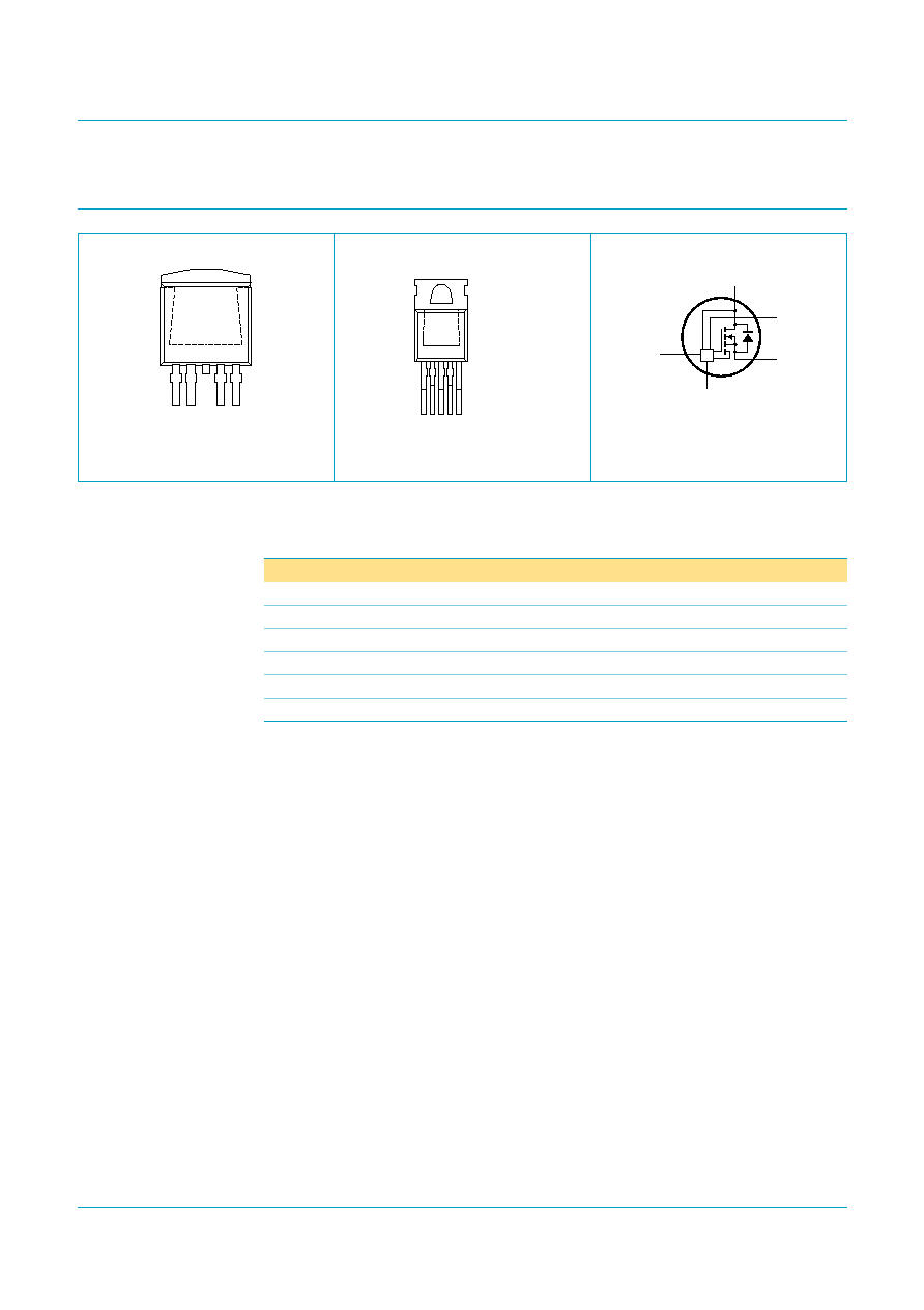
1.1 Description
Monolithic temperature and overload protected single high-side power switch based
on TOPFETTM Trench technology in a 5-pin surface mount or leadform plastic
package.
Product availability:
BUK208-50Y in SOT263B-01
BUK213-50Y in SOT426 (D
2
-PAK).
1.2 Features
1.3 Applications
1.4 Quick reference data
s
Very low quiescent current
s
CMOS logic capability
s
Power TrenchMOSTM
s
Negative load clamping
s
Overtemperature protection
s
Overload protection
s
Over and undervoltage protection
s
ESD protection for all pins
s
Reverse battery protection
s
Diagnostic status indication
s
Low charge pump noise
s
Operating voltage down to 5.5 V
s
Loss of ground protection
s
Current limitation.
s
12 and 24V grounded loads
s
High inrush current loads
s
Inductive loads
s
Replacement for relays and fuses.
Table 1:
Quick reference data
Symbol
Parameter
Min
Max
Unit
R
BLon
on-state resistance at 25
°
C
-
100
m
I
L
continuous load current
-
8.5
A
I
L(nom)
nominal load current (ISO)
3.6
-
A
I
L(lim)
limiting load current
12
24
A
V
BG
operating voltage
5.5
35
V
Philips Semiconductors
BUK208-50Y; BUK213-50Y
Single channel high-side TOPFETTM
Product data
Rev. 02 -- 06 June 2002
2 of 16
9397 750 09384
© Koninklijke Philips Electronics N.V. 2002. All rights reserved.
2.
Pinning information
2.1 Pin description
[1]
It is not possible to make a connection to pin 3 of the SOT426 package.
[2]
The battery is connected to the mounting base.
Fig 1.
Pinning; SOT426 (D
2
-PAK).
Fig 2.
Pinning; SOT263B-01.
Fig 3.
Symbol; (HSS) TOPFET
TM
.
MBL431
1 2
4
3
mb
5
1
5
mb
MBL264
03pa56
I
S
G
B
L
P
Table 2:
Pin description
Symbol
Pin
I/O
Description
G
1
-
circuit common ground
I
2
I
input
B
3
-
[1] [2]
battery
S
4
O
status
L
5
O
load
-
mb
-
[2]
mounting base
Philips Semiconductors
BUK208-50Y; BUK213-50Y
Single channel high-side TOPFETTM
Product data
Rev. 02 -- 06 June 2002
3 of 16
9397 750 09384
© Koninklijke Philips Electronics N.V. 2002. All rights reserved.
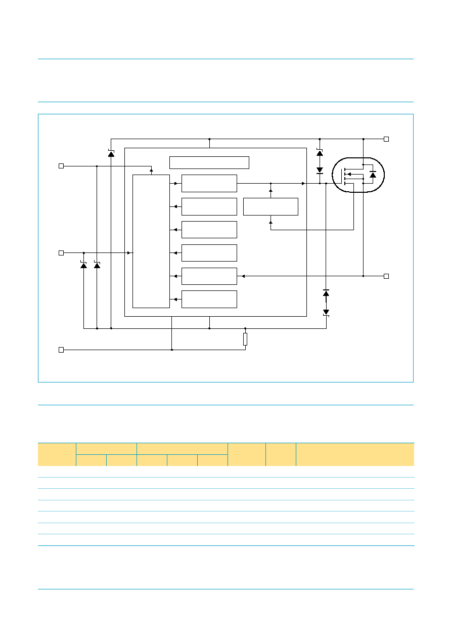
3.
Block diagram
4.
Functional description
[1]
The status will continue to indicate OT (even if the input goes LOW) until the device cools below the reset threshold.
See "Overtemperature protection" characteristics in
Table 6
.
Fig 4.
Elements of the high-side TOPFET switch.
03pa33
RG
input
CONTROL
LOGIC
UNDERVOLTAGE
PROTECTION
OVERVOLTAGE
PROTECTION
LOW CURRENT
DETECT
TEMPERATURE
SENSOR
SHORT CIRCUIT
PROTECTION
CURRENT LIMIT
POWER
MOSFET
load
5
battery
3/mb
CHARGE PUMP
VOLTAGE REGULATOR
2
ground
1
status
4
Table 3:
Truth table
Abbreviations: L = logic LOW; H = logic HIGH; X = don't care; 0 = condition not present; 1 = condition present;
UV = undervoltage; OV = overvoltage; LC = low current or open circuit load; SC = short circuit; OT = overtemperature
[1]
.
Input
Supply
Load
Load
output
Status
Operating mode
UV
OV
LC
SC
OT
L
X
X
X
X
X
OFF
H
off
H
0
0
0
0
0
ON
H
on & normal
H
0
0
1
0
0
ON
L
on & low current detect
H
1
0
X
X
X
OFF
H
supply undervoltage lockout
H
0
1
X
0
0
OFF
H
supply overvoltage shutdown
H
0
0
0
1
X
OFF
L
SC tripped
H
0
0
0
0
1
OFF
L
OT shutdown

Philips Semiconductors
BUK208-50Y; BUK213-50Y
Single channel high-side TOPFETTM
Product data
Rev. 02 -- 06 June 2002
4 of 16
9397 750 09384
© Koninklijke Philips Electronics N.V. 2002. All rights reserved.
5.
Limiting values
[1]
Reverse battery voltage is only allowed with external resistors to limit the input and status currents to a safe value. The connected load
must limit the reverse current. The internal ground resistor limits the reverse battery ground current.
[2]
To limit input current during reverse battery and transient overvoltages.
[3]
To limit status current during reverse battery and transient overvoltages.
6.
Thermal characteristics
Table 4:
Limiting values
In accordance with the Absolute Maximum Rating System (IEC 60134).
Symbol
Parameter
Conditions
Min
Max
Unit
V
BG
continuous supply voltage
-
50
V
I
L
continuous load current
T
mb
112
°
C
-
8.5
A
P
tot
total power dissipation
T
mb
25
°
C
-
48
W
T
stg
storage temperature
-
55
+175
°
C
T
j
junction temperature
-
150
°
C
T
mb
mounting base temperature
during soldering (
10 s)
-
260
°
C
Reverse battery voltage
V
BG
continuous reverse voltage
[1]
-
16
V
V
BG
repetitive reverse voltage
-
32
V
External resistor
R
I
external resistor
[2]
3.3
-
k
R
S
[3]
3.3
-
k
Input current
I
I
continuous current
-
5
+5
mA
I
I
repetitive peak current
0.1; t
p
= 300
µ
s
-
50
+50
mA
Status current
I
S
continuous current
-
5
+5
mA
I
S
repetitive peak current
0.1; t
p
= 300
µ
s
-
50
+50
mA
Inductive load clamping
E
BL(CL)
non-repetitive clamping energy
T
j
= 150
°
C prior to turn-off; I
L
= 2 A
-
100
mJ
Electrostatic discharge
V
esd
electrostatic discharge voltage
Human body model; C = 100 pF;
R = 1.5 k
-
2
kV
Table 5:
Thermal characteristics
Symbol
Parameter
Conditions
Min
Typ
Max
Unit
R
th(j-mb)
thermal resistance from junction to
mounting base
-
2.1
2.6
K/W
R
th(j-a)
thermal resistance from junction to
ambient
mounted on printed circuit board;
minimum footprint; SOT426
-
-
50
K/W

Philips Semiconductors
BUK208-50Y; BUK213-50Y
Single channel high-side TOPFETTM
Product data
Rev. 02 -- 06 June 2002
5 of 16
9397 750 09384
© Koninklijke Philips Electronics N.V. 2002. All rights reserved.
7.
Static characteristics
Table 6:
Static characteristics
Limits are valid for
-
40
°
C
T
mb
+150
°
C and typical values for T
mb
= 25
°
C unless otherwise specified.
Symbol
Parameter
Conditions
Min
Typ
Max
Unit
Clamping voltage
V
BG
battery-ground voltage
I
G
= 1 mA;
Figure 6
50
55
65
V
V
BL
battery-load voltage
I
L
= I
G
= 1 mA
50
55
65
V
V
LG
negative load-ground
I
L
= 10 mA;
Figure 12
and
14
-
18
-
23
-
28
V
V
LG
negative load voltage
I
L
= 2 A; t
p
= 300
µ
s
[1]
-
20
-
25
-
30
V
Supply voltage
V
BG
operating range
battery-ground
5.5
-
35
V
Current
I
B
quiescent current
V
LG
= 0 V;
Figure 10
[2]
T
mb
= 150
°
C
-
-
20
µ
A
T
mb
= 25
°
C
-
0.1
2
µ
A
I
L
off-state load current
V
BL
= V
BG
T
mb
= 150
°
C
-
-
20
µ
A
T
mb
= 25
°
C
-
0.1
1
µ
A
I
G
operating current
Figure 6
-
2
4
mA
I
L(nom)
nominal load current (ISO)
V
BL
= 0.5 V; T
mb
= 85
°
C
[3]
3.6
-
-
A
Resistance
[4]
R
BLon
on-state resistance
9
V
BG
35 V; I
L
= 2 A;
Figure 5
T
mb
= 25
°
C
-
80
100
m
T
mb
= 150
°
C
-
-
200
m
V
BG
= 6 V; I
L
= 2 A
T
mb
= 25
°
C
-
100
125
m
T
mb
= 150
°
C
-
-
250
m
R
G
internal ground resistance
I
G
= 10 mA
95
150
190
Input
[5]
I
I
input current
V
IG
= 5 V
20
90
160
µ
A
V
IG
input clamping voltage
I
I
= 200
µ
A
5.5
7
8.5
V
V
IG(ON)
input turn-on threshold voltage
Figure 9
-
2.4
3
V
V
IG(OFF)
input turn-off threshold voltage
1.5
2.1
-
V
V
IG
input turn-on threshold hysteresis
-
0.3
-
V
I
I(ON)
input turn-on current
V
IG
= 3 V
-
-
100
µ
A
I
I(OFF)
input turn-off current
V
IG
= 1.5 V
10
-
-
µ
A
Low current detection
[6][9]
I
L(LC)
low current detection threshold
T
mb
=
-
40 to +150
°
C
90
-
600
mA
T
mb
= 25
°
C;
Figure 15
150
300
450
mA
I
L(LC)
hysteresis
-
60
-
mA
Undervoltage
[9]
V
BG(UV)
low supply threshold voltage
[7]
2
4.2
5.5
V