Philips Semiconductors
Product specification
Silicon Diffused Power Transistor
BU508AF
GENERAL DESCRIPTION
High voltage, high-speed switching npn transistors in a fully isolated SOT199 envelope, primarily for use in
horizontal deflection circuits of colour television receivers.
QUICK REFERENCE DATA
SYMBOL
PARAMETER
CONDITIONS
TYP.
MAX.
UNIT
V
CESM
Collector-emitter voltage peak value
V
BE
= 0 V
-
1500
V
V
CEO
Collector-emitter voltage (open base)
-
700
V
I
C
Collector current (DC)
-
8
A
I
CM
Collector current peak value
-
15
A
P
tot
Total power dissipation
T
hs
25 �C
-
34
W
V
CEsat
Collector-emitter saturation voltage
I
C
= 4.5 A; I
B
= 1.6 A
-
1.0
V
I
Csat
Collector saturation current
f = 16 kHz
4.5
-
A
t
f
Fall time
I
Csat
= 4.5 A; f = 16kHz
0.7
-
�
s
PINNING - SOT199
PIN CONFIGURATION
SYMBOL
PIN
DESCRIPTION
1
base
2
collector
3
emitter
case isolated
LIMITING VALUES
Limiting values in accordance with the Absolute Maximum Rating System (IEC 134)
SYMBOL
PARAMETER
CONDITIONS
MIN.
MAX.
UNIT
V
CESM
Collector-emitter voltage peak value
V
BE
= 0 V
-
1500
V
V
CEO
Collector-emitter voltage (open base)
-
700
V
I
C
Collector current (DC)
-
8
A
I
CM
Collector current peak value
-
15
A
I
B
Base current (DC)
-
4
A
I
BM
Base current peak value
-
6
A
P
tot
Total power dissipation
T
hs
25 �C
-
34
W
T
stg
Storage temperature
-65
150
�C
T
j
Junction temperature
-
150
�C
THERMAL RESISTANCES
SYMBOL
PARAMETER
CONDITIONS
TYP.
MAX.
UNIT
R
th j-hs
Junction to heatsink
without heatsink compound
-
3.7
K/W
R
th j-hs
Junction to heatsink
with heatsink compound
-
2.8
K/W
R
th j-a
Junction to ambient
in free air
35
-
K/W
1
2
3
case
b
c
e
July 1998
1
Rev 1.200

Philips Semiconductors
Product specification
Silicon Diffused Power Transistor
BU508AF
ISOLATION LIMITING VALUE & CHARACTERISTIC
T
hs
= 25 �C unless otherwise specified
SYMBOL
PARAMETER
CONDITIONS
MIN.
TYP.
MAX.
UNIT
V
isol
Repetitive peak voltage from all
R.H.
65 % ; clean and dustfree
-
2500
V
three terminals to external
heatsink
C
isol
Capacitance from T2 to external f = 1 MHz
-
22
-
pF
heatsink
STATIC CHARACTERISTICS
T
hs
= 25 �C unless otherwise specified
SYMBOL
PARAMETER
CONDITIONS
MIN.
TYP.
MAX.
UNIT
I
CES
Collector cut-off current
1
V
BE
= 0 V; V
CE
= V
CESMmax
-
-
1.0
mA
I
CES
V
BE
= 0 V; V
CE
= V
CESMmax
;
-
-
2.0
mA
T
j
= 125 �C
I
EBO
Emitter cut-off current
V
EB
= 6.0 V; I
C
= 0 A
-
-
10
mA
V
CEOsus
Collector-emitter sustaining voltage
I
B
= 0 A; I
C
= 100 mA;
700
-
-
V
L = 25 mH
V
CEsat
Collector-emitter saturation voltages I
C
= 4.5 A; I
B
= 1.6 A
-
-
1.0
V
V
BEsat
Base-emitter saturation voltage
I
C
= 4.5 A; I
B
= 2 A
-
-
1.1
V
h
FE
DC current gain
I
C
= 100 mA; V
CE
= 5 V
6
13
30
-
DYNAMIC CHARACTERISTICS
T
hs
= 25 �C unless otherwise specified
SYMBOL
PARAMETER
CONDITIONS
TYP.
MAX.
UNIT
f
T
Transition frequency at f = 5 MHz
I
C
= 0.1 A;V
CE
= 5 V
7
-
MHz
C
C
Collector capacitance at f = 1MHz
V
CB
= 10 V
125
-
pF
Switching times (16 kHz line
I
Csat
= 4.5 A;L
c
1 mH;C
fb
= 4 nF
deflection circuit)
I
B(end)
= 1.4 A; L
B
= 6
�
H; -V
BB
= -4 V;
-I
BM
= 2.25 A
t
s
Turn-off storage time
6.5
-
�
s
t
f
Turn-off fall time
0.7
-
�
s
1 Measured with half sine-wave voltage (curve tracer).
July 1998
2
Rev 1.200
Philips Semiconductors
Product specification
Silicon Diffused Power Transistor
BU508AF
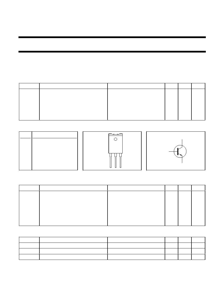
Fig.1. Test circuit for V
CEOsust
.
Fig.2. Oscilloscope display for V
CEOsust
.
Fig.3. Switching times waveforms.
Fig.4. Switching times definitions.
Fig.5. Switching times test circuit.
Fig.6. Typical DC current gain. h
FE
= f (I
C
)
parameter V
CE
+ 50v
100-200R
Horizontal
Vertical
Oscilloscope
1R
6V
30-60 Hz
100R
ICsat
90 %
10 %
tf
ts
IBend
IC
IB
t
t
- IBM
VCE / V
min
VCEOsust
IC / mA
100
200
250
0
+ 150 v nominal
adjust for ICsat
1mH
BY228
12nF
D.U.T.
LB
IBend
-VBB
IC
IB
VCE
ICsat
IBend
64us
26us
20us
t
t
t
TRANSISTOR
DIODE
0.1
1
10
1
10
100
IC/A
h
FE
BU508AD
July 1998
3
Rev 1.200

Philips Semiconductors
Product specification
Silicon Diffused Power Transistor
BU508AF
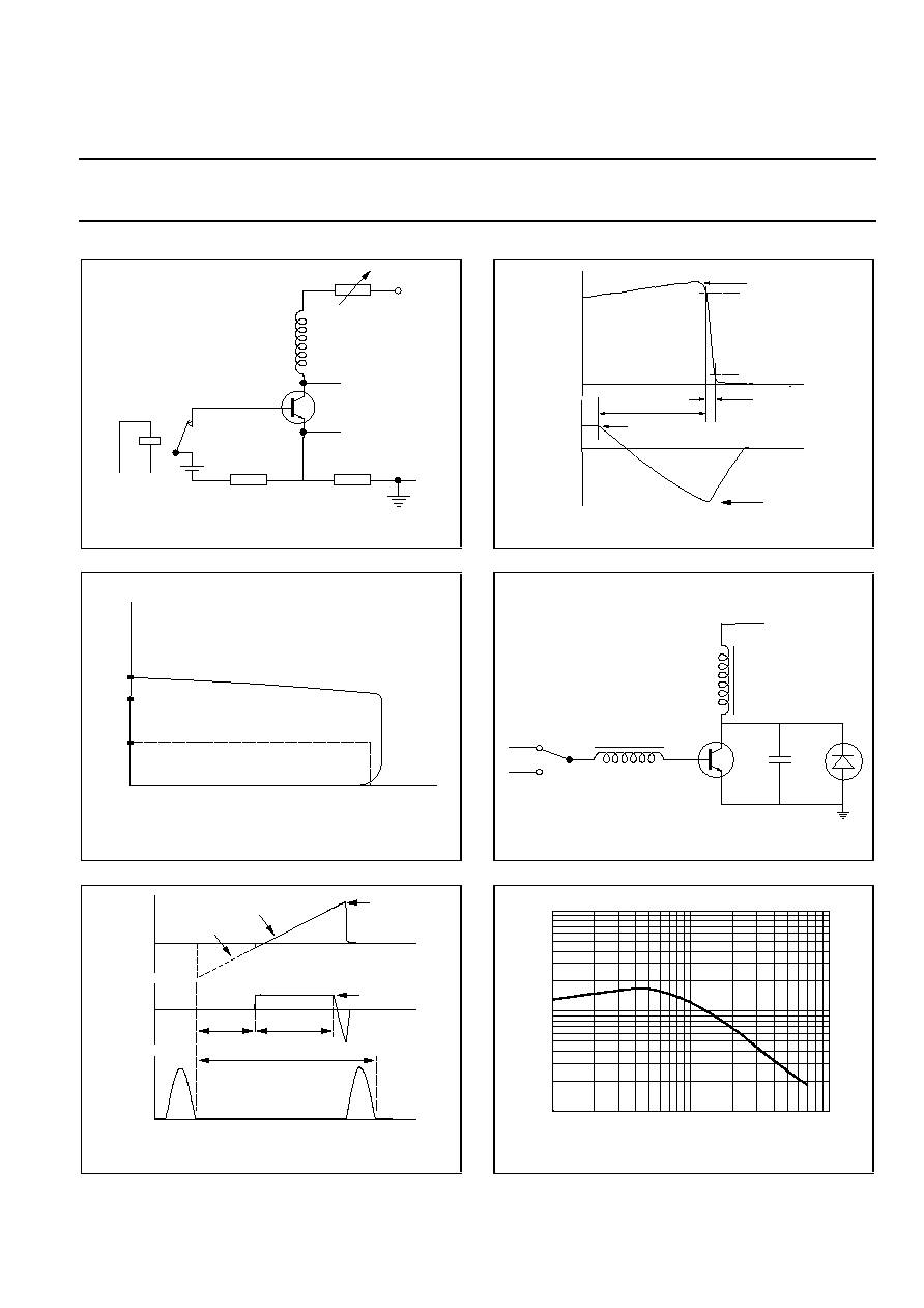
Fig.7. Typical collector-emitter saturation voltage.
V
CE
sat = f (I
C
); parameter I
C
/I
B
Fig.8. Typical base-emitter saturation voltage.
V
BE
sat = f (I
B
); parameter I
C
Fig.9. Typical collector-emitter saturation voltage.
V
CE
sat = f (I
B
); parameter I
C
Fig.10. Transient thermal impedance.
Z
th j-hs
= f(t); parameter D = t
p
/T
Fig.11. Normalised power dissipation.
PD% = 100
P
D
/P
D 25�C
= f (T
hs
)
BU508AD
0.1
1
10
0
0.2
0.4
0.6
0.8
1
IC / A
VCESAT / V
0.1
0.3
0.5
0.7
0.9
1.0E-07
1.0E-05
1E-03
1.0E-01
1.0E+1
0.001
0.01
0.1
1
10
0
0.2
0.1
0.05
0.02
0.5
bu508ax
t / s
Zth K/W
D =
t
p
t
p
T
T
P
t
D
0
1
2
3
4
0.6
0.8
1
1.2
1.4
IC = 6A
IC = 4.5A
IC = 3A
IB / A
VBESAT / V
BU508AD
0
20
40
60
80
100
120
140
Ths / C
PD%
Normalised Power Derating
120
110
100
90
80
70
60
50
40
30
20
10
0
with heatsink compound
BU508AD
0.1
1
10
0.1
1
10
IC = 4.5A
IC = 6A
IC = 3A
VCESAT/V
IB/A
July 1998
4
Rev 1.200
Philips Semiconductors
Product specification
Silicon Diffused Power Transistor
BU508AF
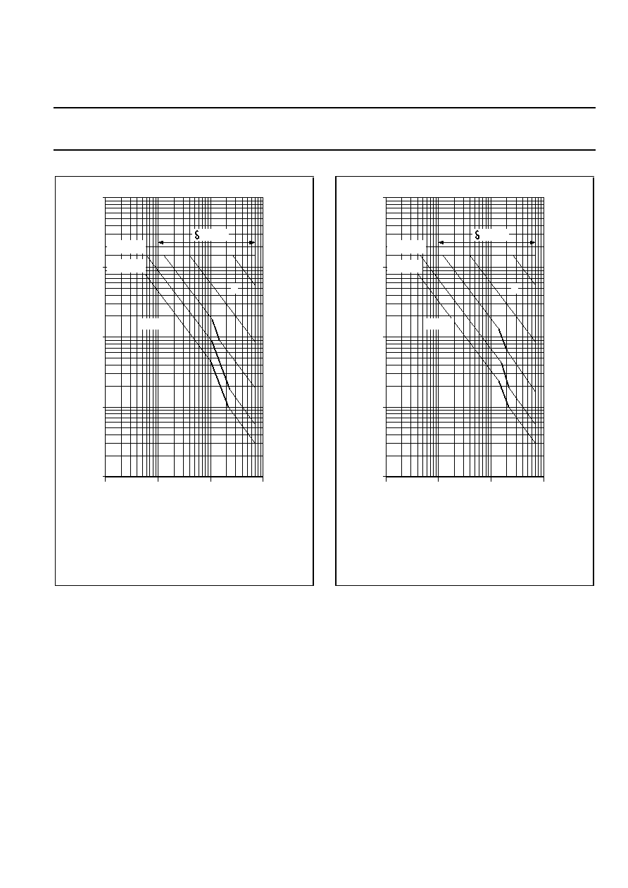
Fig.12. Forward bias safe operating area. T
hs
= 25�C
I
Region of permissible DC operation.
II
Extension for repetitive pulse operation.
NB:
Mounted with heatsink compound and
30
�
5 newton force on the centre of
the envelope.
Fig.13. Forward bias safe operating area. T
hs
= 25�C
I
Region of permissible DC operation.
II
Extension for repetitive pulse operation.
NB:
Mounted without heatsink compound and
30
�
5 newton force on the centre of
the envelope.
1
10
100
1000
100
10
1
0.1
0.01
tp =
10 us
100 us
1 ms
10 ms
DC
IC / A
VCE / V
ICM max
IC max
= 0.01
II
I
Ptot max
1
10
100
1000
100
10
1
0.1
0.01
tp =
10 us
100 us
1 ms
10 ms
DC
IC / A
VCE / V
ICM max
IC max
= 0.01
II
I
Ptot max
July 1998
5
Rev 1.200