
DATA SHEET
Product specification
Supersedes data of April 1995
File under Discrete Semiconductors, SC13b
1997 Jun 20
DISCRETE SEMICONDUCTORS
BST76A
N-channel enhancement mode
vertical D-MOS transistor
1997 Jun 20
2
Philips Semiconductors
Product specification
N-channel enhancement mode
vertical D-MOS transistor
BST76A
FEATURES
·
Direct interface to C-MOS, TTL, etc.
·
High-speed switching
·
No secondary breakdown.
APPLICATIONS
·
Line current interrupter in telephone sets
·
Relay, high-speed and line transformer drivers.
DESCRIPTION
N-channel enhancement mode vertical D-MOS transistor
in a SOT54 (TO-92) variant package.
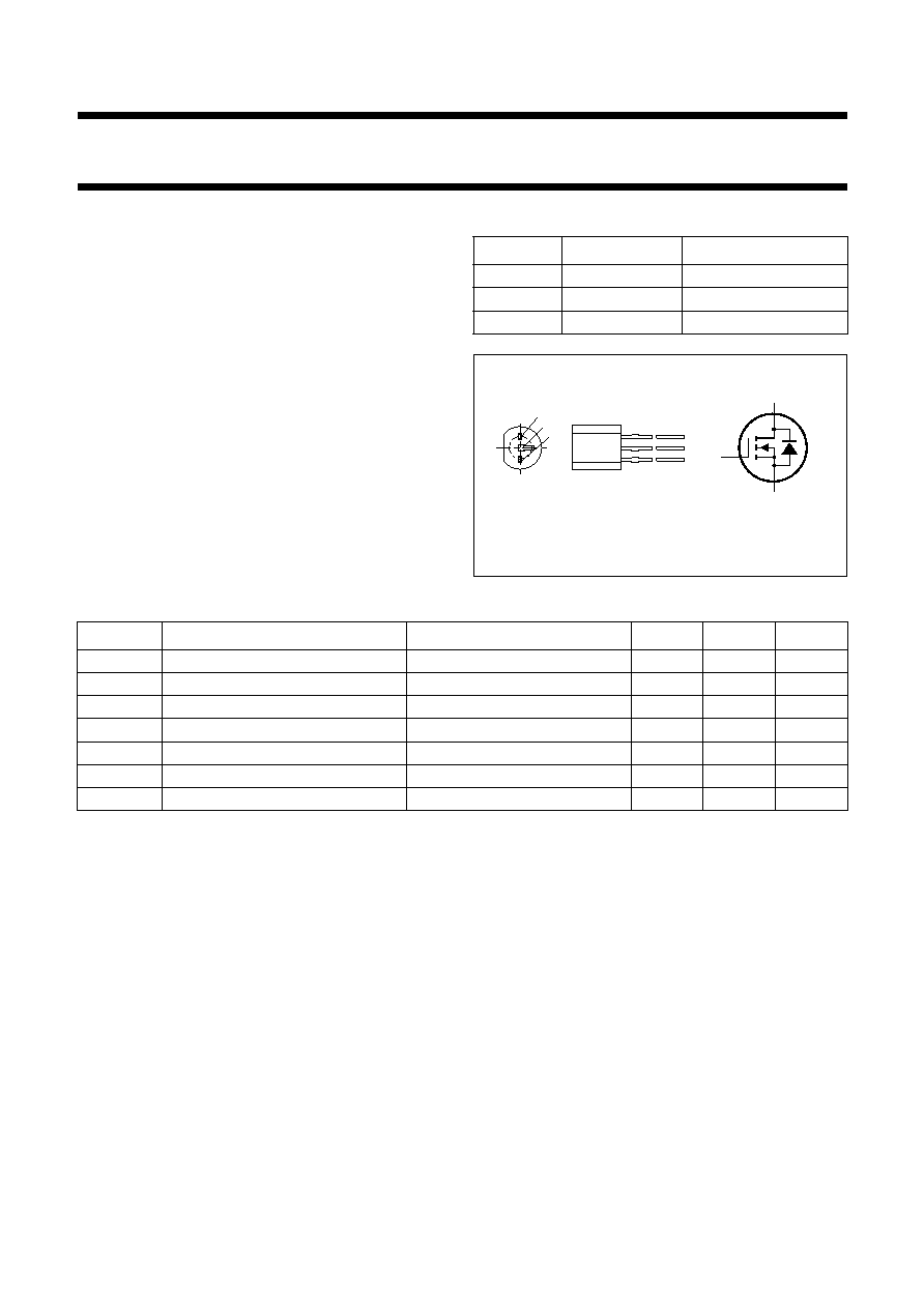
PINNING - SOT54 (TO-92) variant
PIN
SYMBOL
DESCRIPTION
1
s
source
2
g
gate
3
d
drain
Fig.1 Simplified outline and symbol.
handbook, halfpage
1
3
2
MAM146
s
d
g
QUICK REFERENCE DATA
SYMBOL
PARAMETER
CONDITIONS
TYP.
MAX.
UNIT
V
DS
drain-source voltage (DC)
-
180
V
V
DS(SM)
drain-source voltage
non-repetitive peak; t
p
2 mS
-
200
V
V
GSO
gate-source voltage (DC)
open drain
-
±
20
V
I
D
drain current (DC)
-
300
mA
P
tot
total power dissipation
T
amb
25
°
C
-
1
W
R
DSon
drain-source on-state resistance
I
D
= 15 mA; V
GS
= 3 V
7
10
y
fs
forward transfer admittance
I
D
= 300 mA; V
DS
= 15 V
250
-
mS
1997 Jun 20
3
Philips Semiconductors
Product specification
N-channel enhancement mode
vertical D-MOS transistor
BST76A
LIMITING VALUES
In accordance with the Absolute Maximum Rating System (IEC 134).
THERMAL CHARACTERISTICS
Note to the Limiting values and Thermal characteristics
1. Device mounted on a printed-circuit board, maximum lead length 4 mm; mounting pad for drain lead minimum
10 mm
×
10 mm.
CHARACTERISTICS
T
j
= 25
°
C unless otherwise specified.
SYMBOL
PARAMETER
CONDITIONS
MIN.
MAX.
UNIT
V
DS
drain-source voltage (DC)
-
180
V
V
DS(SM)
drain-source voltage
non-repetitive peak; t
p
2 mS
-
200
V
V
GSO
gate-source voltage (DC)
open drain
-
±
20
V
I
D
drain current (DC)
-
300
mA
I
DM
peak drain current
-
800
mA
P
tot
total power dissipation
T
amb
25
°
C; note 1
-
1
W
T
stg
storage temperature
-
65
+150
°
C
T
j
junction temperature
-
150
°
C
SYMBOL
PARAMETER
CONDITIONS
VALUE
UNIT
R
th j-a
thermal resistance from junction to ambient
note 1
125
K/W
SYMBOL
PARAMETER
CONDITIONS
MIN.
TYP.
MAX.
UNIT
V
(BR)DSS
drain-source breakdown voltage
V
GS
= 0; I
D
= 100
µ
A
180
-
-
V
V
GSth
gate-source threshold voltage
V
DS
= V
GS
; I
D
= 100
µ
A
0.7
-
2.4
V
I
DSS
drain-source leakage current
V
DS
= 120 V; V
GS
= 0
-
-
10
µ
A
I
GSS
gate leakage current
V
DS
= 0; V
GS
=
±
20 V
-
-
±
100
nA
R
DSon
drain-source on-state resistance
V
GS
= 3 V; I
D
= 15 mA
-
7
10
V
GS
= 10 V; I
D
= 300 mA
-
6
-
y
fs
forward transfer admittance
I
D
= 300 mA; V
DS
= 15 V
-
250
-
mS
C
iss
input capacitance
V
DS
= 10 V; V
GS
= 0; f = 1 MHz
-
50
65
pF
C
oss
output capacitance
V
DS
= 10 V; V
GS
= 0; f = 1 MHz
-
20
30
pF
C
rss
reverse transfer capacitance
V
DS
= 10 V; V
GS
= 0; f = 1 MHz
-
6
10
pF
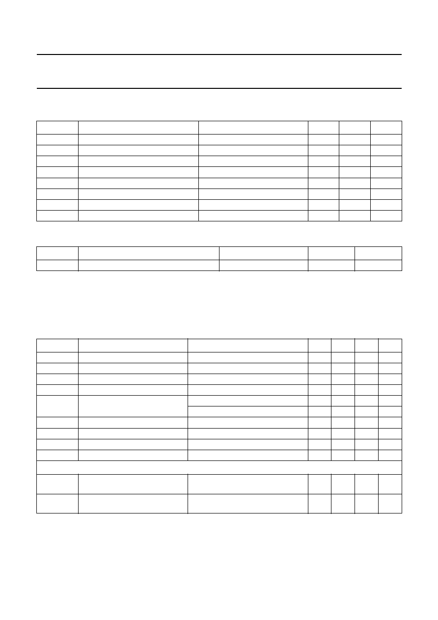
Switching times (see Figs 2 and 3)
t
on
turn-on time
V
GS
= 0 to 10 V; V
DS
= 50 V;
I
D
= 300 mA
-
-
10
ns
t
off
turn-off time
V
GS
= 10 to 0 V; V
DS
= 50 V;
I
D
= 300 mA
-
-
15
ns
1997 Jun 20
4
Philips Semiconductors
Product specification
N-channel enhancement mode
vertical D-MOS transistor
BST76A
Fig.2 Switching times test circuit.
handbook, halfpage
MSA631
50
V = 50 V
DD
I D
10 V
0 V
Fig.3 Input and output waveforms.
handbook, halfpage
MBB692
10 %
90 %
90 %
10 %
t on
t off
OUTPUT
INPUT
Fig.4 Power derating curve.
handbook, halfpage
0
200
0
0.4
0.8
1.2
MLC697
T ( C)
amb
o
50
100
150
Ptot
(W)
Fig.5
Capacitance as a function of drain-source
voltage; typical values.
V
GS
= 0; f = 1 MHz; T
j
= 25
°
C.
(1) C
iss
.
(2) C
oss
.
(3) C
rss
.
handbook, halfpage
0
120
80
40
0
C
(pF)
VDS (V)
10
20
30
MDA168
(1)
(2)
(3)
1997 Jun 20
5
Philips Semiconductors
Product specification
N-channel enhancement mode
vertical D-MOS transistor
BST76A
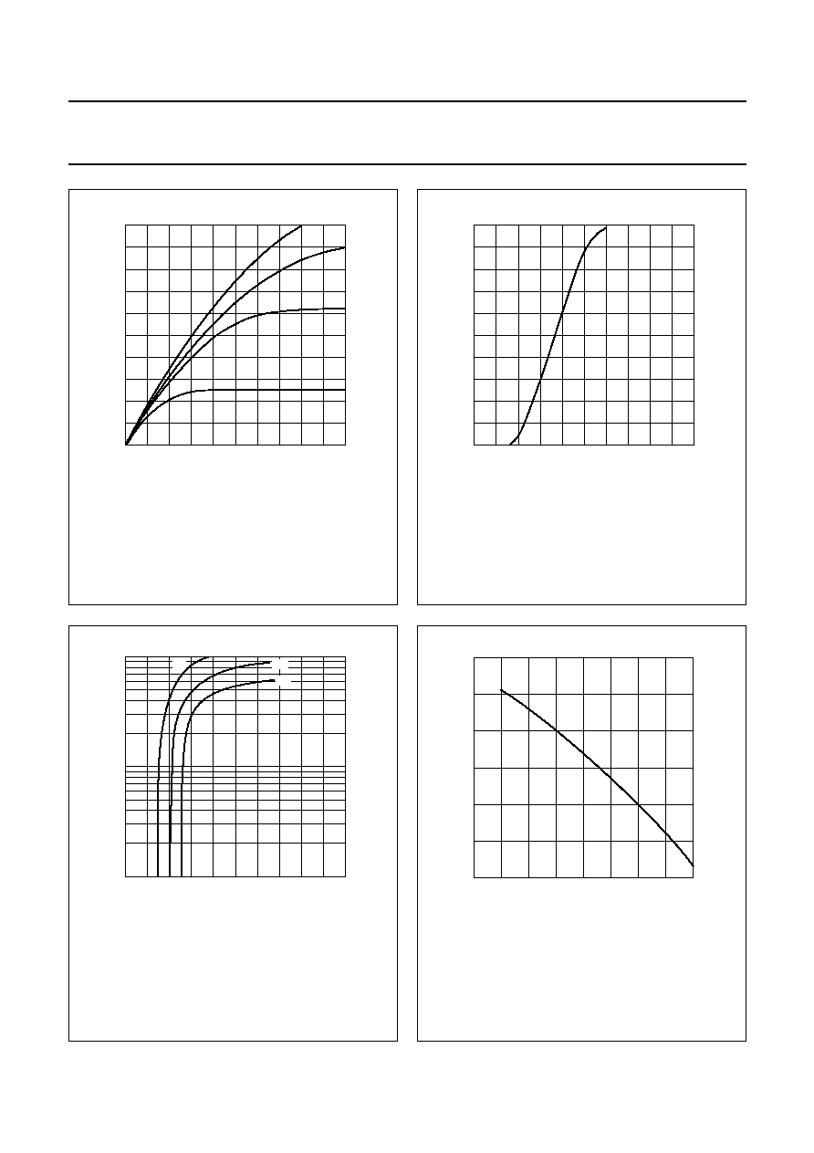
Fig.6 Output characteristics; typical values.
T
j
= 25
°
C.
(1) V
GS
= 10 V.
(2) V
GS
= 5 V.
(3) V
GS
= 4 V.
(4) V
GS
= 3 V.
handbook, halfpage
0
(1)
(2)
(3)
(4)
10
1
0
VDS (V)
ID
(A)
0
.
2
0
.
4
0
.
6
0
.
8
2
4
6
8
MDA164
Fig.7 Transfer characteristic; typical values.
V
DS
= 10 V; T
j
= 25
°
C.
handbook, halfpage
0
10
1
0
VGS (V)
ID
(A)
0
.
2
0
.
4
0
.
6
0
.
8
2
4
6
8
MDA170
Fig.8
Drain current as a function of drain-source
on-state resistance; typical values.
T
j
= 25
°
C.
(1) V
GS
= 10 V.
(2) V
GS
= 5 V.
(3) V
GS
= 4 V.
handbook, halfpage
14
4
ID
(mA)
RDSon (
)
6
8
10
12
10
3
10
2
10
MDA169
(1)
(2)
(3)
Fig.9
Temperature coefficient of gate-source
threshold voltage; typical values.
V
GSth
at 0.1 mA.
k
V
GSth
at T
j
V
GSth
at 25
°
C
--------------------------------------
=
handbook, halfpage
-
50
1.2
1
0.8
0.6
k
0
50
150
100
MDA167
Tj (
o
C)