
DATA SHEET
Product specification
Supersedes data of April 1995
File under Discrete Semiconductors, SC13b
1997 Jun 19
DISCRETE SEMICONDUCTORS
BSS92
P-channel enhancement mode
vertical D-MOS transistor
1997 Jun 19
2
Philips Semiconductors
Product specification
P-channel enhancement mode
vertical D-MOS transistor
BSS92
FEATURES
À
Direct interface to C-MOS, TTL, etc.
À
High-speed switching
À
No secondary breakdown.
APPLICATIONS
À
Line current interrupter in telephony applications
À
Relay, high speed and line transformer drivers.
DESCRIPTION
P-channel enhancement mode vertical D-MOS transistor
in a TO-92 (SOT54) variant package.
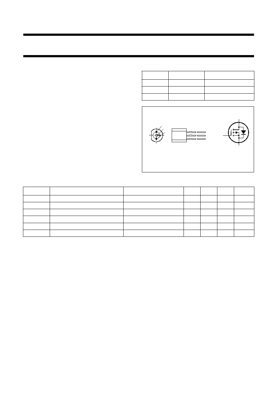
PINNING - TO-92 (SOT54) variant
PIN
SYMBOL
DESCRIPTION
1
g
gate
2
d
drain
3
s
source
Fig.1 Simplified outline and symbol.
handbook, halfpage
s
d
g
MAM144
1
3
2
QUICK REFERENCE DATA
SYMBOL
PARAMETER
CONDITIONS
MIN.
TYP.
MAX.
UNIT
V
DS
drain-source voltage (DC)
-
-
-
240
V
V
GSO
gate-source voltage (DC)
open drain
-
-
▒
20
V
I
D
drain current (DC)
-
-
-
150
mA
R
DSon
drain-source on-state resistance
I
D
=
-
100 mA; V
GS
=
-
10 V
-
10
20
P
tot
total power dissipation
T
amb
25
░
C
-
-
1
W
y
fs
forward transfer admittance
V
DS
=
-
25 V; I
D
=
-
100 mA
60
200
-
mS
1997 Jun 19
3
Philips Semiconductors
Product specification
P-channel enhancement mode
vertical D-MOS transistor
BSS92
LIMITING VALUES
In accordance with the Absolute Maximum Rating System (IEC 134).
THERMAL CHARACTERISTICS
Note to the Limiting values and Thermal characteristics
1. Device mounted on a printed-circuit board, maximum lead length 4 mm; mounting pad for drain lead minimum
10 mm
Î
10 mm.
CHARACTERISTICS
T
j
= 25
░
C unless otherwise specified.
SYMBOL
PARAMETER
CONDITIONS
MIN.
MAX.
UNIT
V
DS
drain-source voltage (DC)
-
-
240
V
V
GSO
gate-source voltage (DC)
open drain
-
▒
20
V
I
D
drain current (DC)
-
-
150
mA
I
DM
peak drain current
-
-
600
mA
P
tot
total power dissipation
T
amb
25
░
C; note 1
-
1
W
T
stg
storage temperature
-
55
+150
░
C
T
j
operating junction temperature
-
150
░
C
SYMBOL
PARAMETER
CONDITIONS
VALUE
UNIT
R
th j-a
thermal resistance from junction to ambient
note 1
125
K/W
SYMBOL
PARAMETER
CONDITIONS
MIN.
TYP.
MAX.
UNIT
V
(BR)DSS
drain-source breakdown voltage
V
GS
= 0; I
D
=
-
250
Á
A
-
240
-
-
V
V
GSth
gate-source threshold voltage
V
DS
= V
GS
; I
D
=
-
1 mA
-
0.8
-
-
2.8
V
I
DSS
drain-source leakage current
V
GS
= 0; V
DS
=
-
60 V
-
-
-
200
nA
V
GS
= 0; V
DS
=
-
200 V
-
-
-
60
Á
A
I
GSS
gate leakage current
V
DS
= 0; V
GS
=
▒
20 V
-
-
▒
100
nA
R
DSon
drain-source on-state resistance
V
GS
=
-
10 V; I
D
=
-
100 mA
-
10
20
y
fs
forward transfer admittance
V
DS
=
-
25 V; I
D
=
-
100 mA
60
200
-
mS
C
iss
input capacitance
V
GS
= 0; V
DS
=
-
25 V; f = 1 MHz
-
65
-
pF
C
oss
output capacitance
V
GS
= 0; V
DS
=
-
25 V; f = 1 MHz
-
20
-
pF
C
rss
reverse transfer capacitance
V
GS
= 0; V
DS
=
-
25 V; f = 1 MHz
-
6
-
pF
Switching times (see Figs 2 and 3)
t
on
turn-on time
V
GS
= 0 to
-
10 V; V
DD
=
-
50 V;
I
D
=
-
250 mA
-
5
-
ns
t
off
turn-off time
V
GS
=
-
10 to 0 V; V
DD
=
-
50 V;
I
D
=
-
250 mA
-
20
-
ns

1997 Jun 19
4
Philips Semiconductors
Product specification
P-channel enhancement mode
vertical D-MOS transistor
BSS92
Fig.2 Switching times test circuit.
handbook, halfpage
MBB689
50
I D
-
10 V
0
V =
-
50 V
DD
Fig.3 Input and output waveforms.
handbook, halfpage
MBB690
10 %
90 %
90 %
10 %
t on
t off
OUTPUT
INPUT
1997 Jun 19
5
Philips Semiconductors
Product specification
P-channel enhancement mode
vertical D-MOS transistor
BSS92
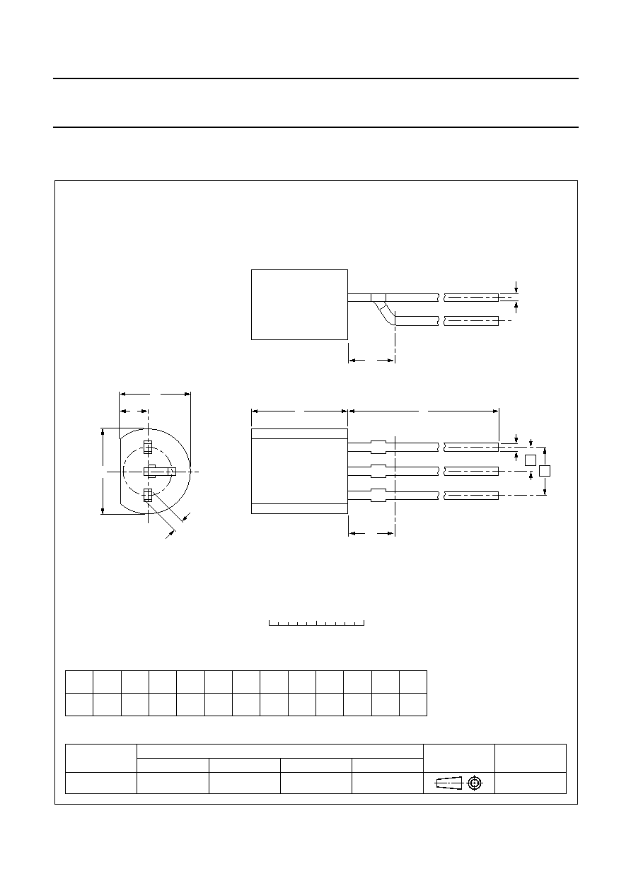
PACKAGE OUTLINE
UNIT
A
REFERENCES
OUTLINE
VERSION
EUROPEAN
PROJECTION
ISSUE DATE
IEC
JEDEC
EIAJ
mm
5.2
5.0
b
0.48
0.40
c
0.45
0.40
D
4.8
4.4
d
1.7
1.4
E
4.2
3.6
L
14.5
12.7
e
2.54
e1
1.27
L1
(1)
max
L2
max
2.5
2.5
b1
0.66
0.56
DIMENSIONS (mm are the original dimensions)
Notes
1. Terminal dimensions within this zone are uncontrolled to allow for flow of plastic and terminal irregularities.
SOT54 variant
TO-92
SC-43
A
L
0
2.5
5 mm
scale
b
c
D
b
1
L1
d
E
Plastic single-ended leaded (through hole) package; 3 leads (on-circle)
SOT54 variant
1
2
3
L2
e1
e
97-04-14