DATA SHEET
Product specification
File under Discrete Semiconductors, SC13b
April 1995
DISCRETE SEMICONDUCTORS
BSP254; BSP254A
P-channel enhancement mode
vertical D-MOS transistor

April 1995
2
Philips Semiconductors
Product specification
P-channel enhancement mode vertical
D-MOS transistor
BSP254; BSP254A
FEATURES
·
Direct interface to C-MOS, TTL,
etc.
·
High-speed switching
·
No secondary breakdown.
DESCRIPTION
P-channel vertical D-MOS transistor
in a TO-92 variant envelope and
intended for use as a line current
interruptor in relay, high-speed and
line transformer drivers.
PINNING - TO-92 variant BSP254
PINNING - TO-92 variant BSP254A
PIN
DESCRIPTION
1
gate
2
drain
3
source
PIN
DESCRIPTION
1
source
2
gate
3
drain
QUICK REFERENCE DATA
SYMBOL
PARAMETER
CONDITIONS
MIN. TYP. MAX. UNIT
V
DS
drain-source
voltage
-
-
-
250
V
V
GSO
gate-source
voltage
open drain
-
-
±
20
V
Y
fs
forward transfer
admittance
I
D
=
-
200 mA;
V
DS
=
-
25V
100
200
-
mS
I
D
drain current (DC)
-
-
-
0.2
A
R
DS(on)
drain-source
on-state resistance
V
GS
=
-
10 V;
I
D
=
-
200 mA
-
10
15
P
tot
total power
dissipation
T
amb
= 25
°
C
-
-
1
W
Fig.1 Simplified outline and symbol.
handbook, halfpage
1
3
2
MAM147
s
d
g

April 1995
3
Philips Semiconductors
Product specification
P-channel enhancement mode vertical
D-MOS transistor
BSP254; BSP254A
LIMITING VALUES
In accordance with the Absolute Maximum System (IEC 134)
THERMAL RESISTANCE
Note
1. Transistor mounted on printed circuit board, maximum lead length 4 mm,
mounting pad for drain lead minimum 10 mm x 10 mm.
SYMBOL
PARAMETER
CONDITIONS
MIN.
MAX.
UNIT
-
V
DS
drain-source voltage
-
250
V
V
GSO
gate-source voltage
open drain
-
20
V
-
I
D
drain current
DC
-
0.2
A
-
I
DM
drain current
peak value
-
0.6
A
P
tot
total power dissipation
T
amb
= 25
°
C (note 1)
-
1
W
T
stg
storage temperature range
-
65
+
150
°
C
T
j
junction temperature
-
150
°
C
SYMBOL
PARAMETER
MAX.
UNIT
R
th j-a
from junction to ambient (note 1)
125
K/W
Fig.2 Power derating curve.
handbook, halfpage
0
1.2
0.8
0.4
0
50
100
200
150
MRC238
Ptot
(W)
Tamb (
°
C)

April 1995
4
Philips Semiconductors
Product specification
P-channel enhancement mode vertical
D-MOS transistor
BSP254; BSP254A
CHARACTERISTICS
T
j
= 25
°
C unless otherwise specified.
Notes
1. Measured at f = 1 MHz;
-
V
DS
= 25 V; V
GS
= 0.
2.
-
V
GS
= 0 to 10 V;
-
I
D
= 250 mA;
-
V
DD
= 50 V.
SYMBOL
PARAMETER
CONDITIONS
MIN.
TYP.
MAX.
UNIT
-
V
(BR)DSS
drain-source breakdown voltage
-
V
GS
= 0
-
I
D
= 10
µ
A
250
-
-
V
-
I
DSS
drain-source leakage current
-
V
DS
= 200 V
V
GS
= 0
-
-
1
µ
A
±
I
GSS
gate-source leakage current
±
V
GS
= 20 V
V
DS
= 0
-
-
100
nA
-
V
GS(th)
gate-source threshold voltage
V
GS
= V
DS
-
I
D
= 1 mA
0.8
-
2.8
V
R
DS(on)
drain-source on-resistance
-
V
GS
= 10 V
-
I
D
= 200 mA;
-
10
15
Y
fs
transfer admittance
-
V
DS
= 25 V
-
I
D
= 200 mA
100
200
-
mS
C
iss
input capacitance
note 1
-
65
90
pF
C
oss
output capacitance
note 1
-
20
30
pF
C
rss
feedback capacitance
note 1
-
6
15
pF
t
on
turn-on time
note 2
-
5
10
ns
t
off
turn-off time
note 2
-
20
30
ns
Fig.3 Switching times test circuit.
handbook, halfpage
MBB689
50
VDD =
-
50 V
ID
0 V
-
10 V
Fig.4 Input and output waveforms.
handbook, halfpage
MBB690
10 %
90 %
90 %
10 %
ton
toff
OUTPUT
INPUT
April 1995
5
Philips Semiconductors
Product specification
P-channel enhancement mode vertical
D-MOS transistor
BSP254; BSP254A
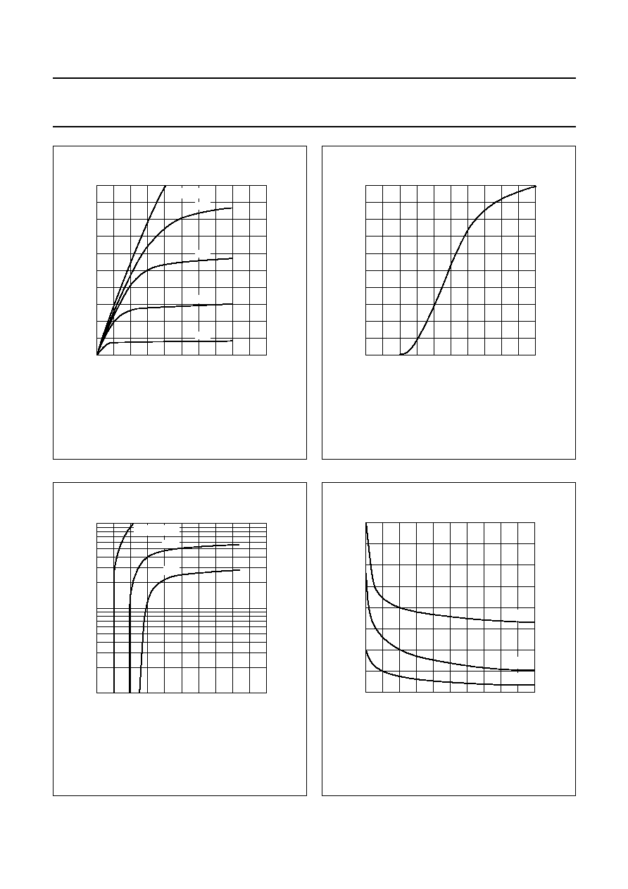
Fig.5 Typical output characteristics; T
j
= 25
°
C.
handbook, halfpage
0
-
25
-
1
0
-
0.2
-
0.4
-
0.6
-
0.8
-
5
-
10
-
15
ID
(A)
-
20
MDA706
VDS (V)
VGS =
-
10 V
-
4 V
-
3 V
-
6 V
-
5 V
Fig.6
Typical transfer characteristic; V
DS
=
-
10 V;
T
j
= 25
°
C.
handbook, halfpage
0
-
10
-
1
0
-
0.2
-
0.4
-
0.6
-
0.8
-
2
-
4
-
6
ID
(A)
-
8
MDA707
VGS (V)
Fig.7
Typical on-resistance as a function of drain
current, T
j
= 25
°
C.
handbook, halfpage
28
8
12
ID
(mA)
RDSon (
)
16
20
24
-
10
3
-
10
2
-
10
MDA708
VGS =
-
10 V
-
5 V
-
4 V
Fig.8
Typical capacitances as a function of
drain-source voltage; V
GS
= 0; f = 1 MHz;
T
j
= 25
°
C.
handbook, halfpage
0
120
160
80
40
0
-
5
-
10
-
25
-
20
-
15
MDA734
C
(pF)
VDS (V)
Crss
Ciss
Coss