Document Outline
- DESCRIPTION
- FEATURES
- PINNING - SOT223
- PIN CONFIGURATION
- QUICK REFERENCE DATA
- RATINGS
- THERMAL RESISTANCE
- CHARACTERISTICS
- PACKAGE OUTLINE
- DEFINITIONS
- LIFE SUPPORT APPLICATIONS
DATA SHEET
Product specification
File under Discrete Semiconductors, SC13b
April 1995
DISCRETE SEMICONDUCTORS
BSP205
P-channel enhancement mode
vertical D-MOS transistor

April 1995
2
Philips Semiconductors
Product specification
P-channel enhancement mode vertical
D-MOS transistor
BSP205
DESCRIPTION
P-channel enhancement mode
vertical D-MOS transistor in a
miniature SOT223 envelope and
intended for use in relay, high-speed
and line-transformer drivers.
FEATURES
·
Very low R
DS(on)
·
Direct interface to C-MOS, TTL,
etc.
·
High-speed switching
·
No secondary breakdown
PINNING - SOT223
1
= gate
2
= drain
3
= source
4
= drain
QUICK REFERENCE DATA
Drain-source voltage
-
V
DS
max.
60 V
Drain current (DC)
-
I
D
max.
275 mA
Drain-source ON-resistance
-
I
D
= 200 mA;
-
V
GS
= 10 V
R
DS(on)
max.
10
Gate threshold voltage
-
V
GS(th)
max.
3.5 V
PIN CONFIGURATION
Marking code
BSP205
Fig.1 Simplified outline and symbol.
handbook, halfpage
MAM121
4
1
2
3
Top view
s
d
g

April 1995
3
Philips Semiconductors
Product specification
P-channel enhancement mode vertical
D-MOS transistor
BSP205
RATINGS
Limiting values in accordance with the Absolute Maximum System (IEC 134)
THERMAL RESISTANCE
Note
1. Device mounted on an epoxy printed-circuit board 40 mm
×
40 mm
×
1.5 mm; mounting pad for the drain lead
min. 6 cm
2
.
Drain-source voltage
-
V
DS
max.
60 V
Gate-source voltage (open drain)
±
V
GSO
max.
20 V
Drain current (DC)
-
I
D
max.
275 mA
Drain current (peak)
-
I
DM
max.
550 mA
Total power dissipation up to T
amb
= 25
°
C (note 1)
P
tot
max.
1.5 W
Storage temperature range
T
stg
-
65 to 150
°
C
Junction temperature
T
j
max.
150
°
C
From junction to ambient (note 1)
R
th j-a
=
83.3 K/W

April 1995
4
Philips Semiconductors
Product specification
P-channel enhancement mode vertical
D-MOS transistor
BSP205
CHARACTERISTICS
T
j
= 25
°
C unless otherwise specified
Drain-source breakdown voltage
-
I
D
= 10
µ
A; V
GS
= 0
-
V
(BR)DSS
min.
60 V
Drain-source leakage current
-
V
DS
= 48 V; V
GS
= 0
-
I
DSS
max.
1.0
µ
A
Gate-source leakage current
±
V
GS
= 20 V; V
DS
= 0
±
I
GSS
max.
100 nA
Gate threshold voltage
min.
max.
1.5
3.5
V
V
-
I
D
= 1 mA; V
DS
= V
GS
-
V
GS(th)
Drain-source ON-resistance
typ.
max.
7.5
10
-
I
D
= 200 mA ;
-
V
GS
= 10 V
R
DS(on)
Transfer admittance
min.
typ.
60
125
mS
mS
-
I
D
= 200 mA;
-
V
DS
= 15 V
Y
fs
Input capacitance at f = 1 MHz;
typ.
max.
30
45
pF
pF
-
V
DS
= 10 V; V
GS
= 0
C
iss
Output capacitance at f = 1 MHz;
typ.
max.
20
30
pF
pF
-
V
DS
= 10 V; V
GS
= 0
C
oss
Feedback capacitance at f = 1 MHz;
typ.
max.
5
10
pF
pF
-
V
DS
= 10 V; V
GS
= 0
C
rss
Switching times (see Figs 2 and 3)
-
I
D
= 200 mA;
-
V
DD
= 50 V;
-
V
GS
= 0 to 10 V
t
on
typ.
max.
3
6
ns
ns
t
off
typ.
max.
10
15
ns
ns
April 1995
5
Philips Semiconductors
Product specification
P-channel enhancement mode vertical
D-MOS transistor
BSP205
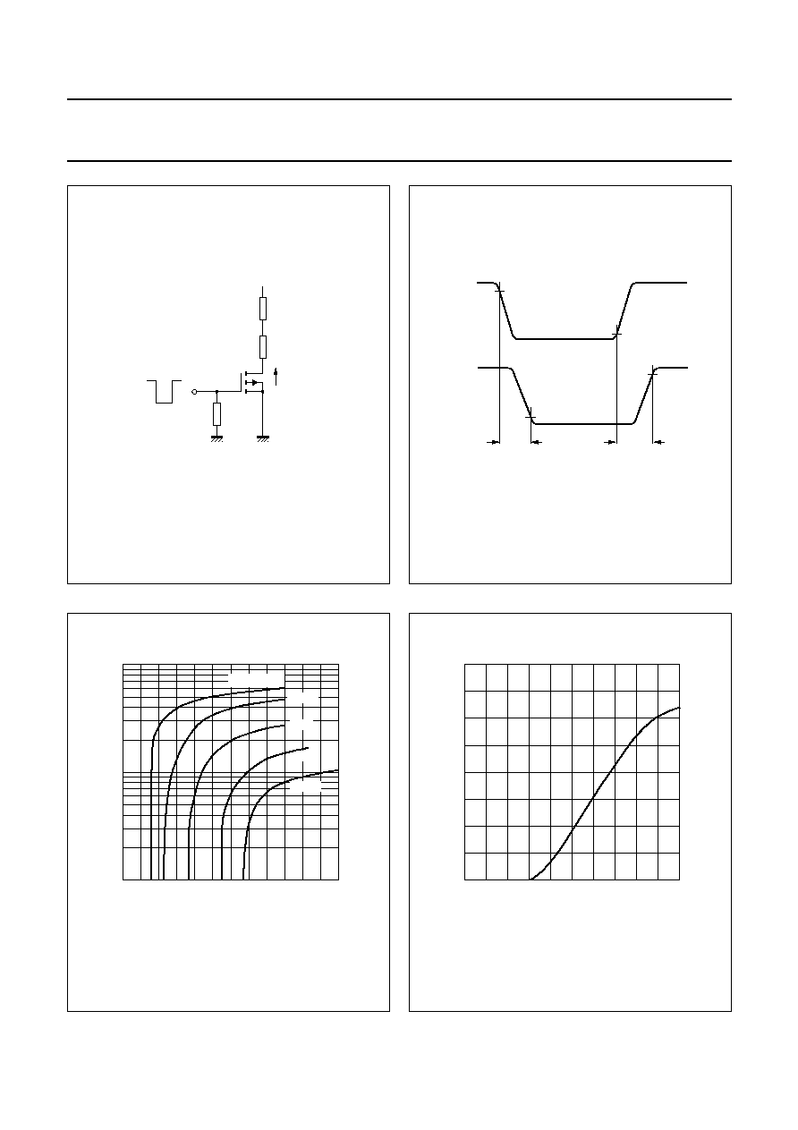
Fig.2 Switching time test circuit.
handbook, halfpage
MBB689
50
VDD =
-
50 V
ID
0 V
-
10 V
Fig.3 Input and output waveforms.
handbook, halfpage
MBB690
10 %
90 %
90 %
10 %
ton
toff
OUTPUT
INPUT
Fig.4
ON-resistance as a function of drain
current; T
j
= 25
°
C; typical values.
handbook, halfpage
18
6
10
8
ID
(mA)
RDSon (
)
12
14
16
-
10
3
-
10
2
-
10
MDA741
VGS =
-
10 V
-
6 V
-
5 V
-
4.5 V
-
7.5 V
Fig.5
Transfer characteristics;
-
V
DS
= 10 V;
T
j
= 25
°
C; typical values.
handbook, halfpage
0
-
0.6
-
0.8
-
0.4
-
0.2
0
-
2
-
4
-
10
-
8
-
6
MDA751
ID
(A)
VGS (V)