
DATA SHEET
Product specification
File under Discrete Semiconductors, SC13b
April 1995
DISCRETE SEMICONDUCTORS
BS108
N-channel enhancement mode
vertical D-MOS transistor

April 1995
2
Philips Semiconductors
Product specification
N-channel enhancement mode vertical
D-MOS transistor
BS108
FEATURES
·
Direct interface to C-MOS, TTL,
etc.
·
High-speed switching
·
No secondary breakdown.
DESCRIPTION
N-channel enhancement mode
vertical D-MOS transistor in a TO-92
envelope, intended for use as a line
current interruptor in telephone sets
and for applications in relay,
high-speed and line transformer
drivers.
PINNING
PIN
DESCRIPTION
1
source
2
gate
3
drain
QUICK REFERENCE DATA
SYMBOL
PARAMETER
MAX.
UNIT
V
DS
drain-source voltage
200
V
I
D
DC drain current
250
mA
R
DS(on)
drain-source on-resistance
8
V
GS(th)
gate-source threshold voltage
1.8
V
Fig.1 Simplified outline (TO-92) and symbol.
handbook, halfpage
1
3
2
MSB033
handbook, 2 columns
s
d
g
MBB076 - 1

April 1995
3
Philips Semiconductors
Product specification
N-channel enhancement mode vertical
D-MOS transistor
BS108
LIMITING VALUES
In accordance with the Absolute Maximum System (IEC 134).
THERMAL RESISTANCE
Note
1. Device mounted on a printed-circuit board, maximum lead length 4 mm; mounting pad for the drain lead minimum
10
×
10 mm
CHARACTERISTICS
T
j
= 25
°
C unless otherwise specified.
SYMBOL
PARAMETER
CONDITIONS
MIN.
MAX.
UNIT
V
DS
drain-source voltage
-
200
V
±
V
GSO
gate-source voltage
open drain
-
20
V
I
D
DC drain current
-
250
mA
I
DM
peak drain current
-
1
A
P
tot
total power dissipation
up to T
amb
= 25
°
C (note 1)
-
1
W
T
stg
storage temperature range
-
65
150
°
C
T
j
junction temperature
-
150
°
C
SYMBOL
PARAMETER
THERMAL RESISTANCE
R
th j-a
from junction to ambient (note 1)
125 K/W
SYMBOL
PARAMETER
CONDITIONS
MIN.
TYP.
MAX. UNIT
V
(BR)DSS
drain-source breakdown voltage
I
D
= 10
µ
A; V
GS
= 0
200
-
-
V
I
DSS
drain-source leakage current
V
DS
= 160 V; V
GS
= 0
-
-
1
µ
A
I
GSS
gate-source leakage current
±
V
GS
= 20 V; V
DS
= 0
-
-
100
nA
V
GS(th)
gate-source threshold voltage
I
D
= 1 mA; V
GS
= V
DS
0.4
-
1.8
V
R
DS(on)
drain-source on-resistance
I
D
= 100 mA; V
GS
= 2.8 V
-
5
8
Y
fs
transfer admittance
I
D
= 300 mA; V
DS
= 25 V
200
400
-
mS
C
iss
input capacitance
V
DS
= 25 V; V
GS
= 0;
f = 1 MHz
-
50
80
pF
C
oss
output capacitance
V
DS
= 25 V; V
GS
= 0;
f = 1 MHz
-
20
30
pF
C
rss
feedback capacitance
V
DS
= 25 V; V
GS
= 0;
f = 1 MHz
-
5
10
pF
Switching times (see Figs 2 and 2)
t
on
turn-on time
I
D
= 250 mA; V
DD
= 50 V;
V
GS
= 0 to 10 V
-
5
10
ns
t
off
turn-off time
I
D
= 250 mA; V
DD
= 50 V;
V
GS
= 0 to 10 V
-
20
30
ns

April 1995
4
Philips Semiconductors
Product specification
N-channel enhancement mode vertical
D-MOS transistor
BS108
Fig.2 Switching times test circuit.
V
DD
= 50 V
handbook, halfpage
MSA631
50
VDD = 50 V
ID
10 V
0 V
Fig.3 Input and output waveforms.
handbook, halfpage
MBB692
10 %
90 %
90 %
10 %
ton
toff
OUTPUT
INPUT
April 1995
5
Philips Semiconductors
Product specification
N-channel enhancement mode vertical
D-MOS transistor
BS108
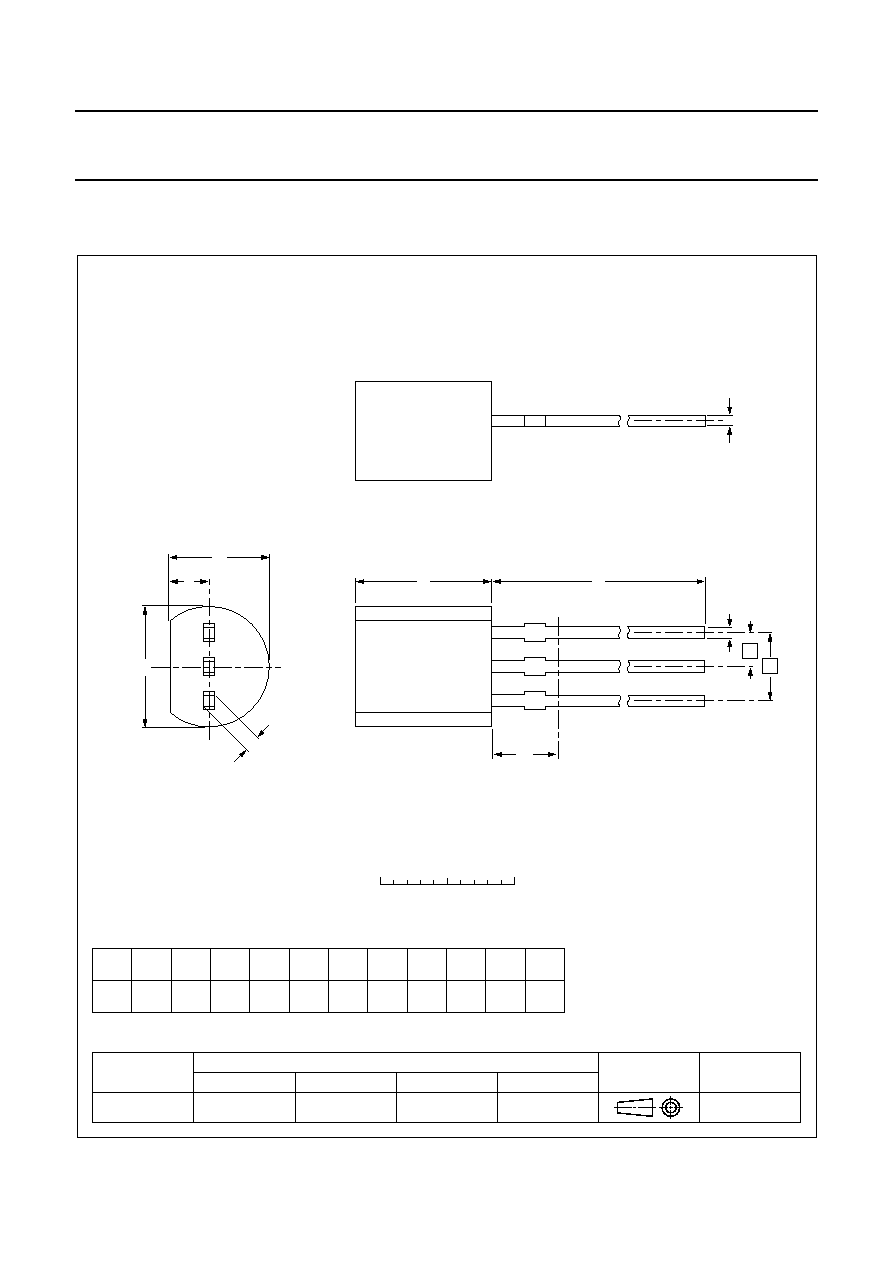
PACKAGE OUTLINE
UNIT
A
REFERENCES
OUTLINE
VERSION
EUROPEAN
PROJECTION
ISSUE DATE
IEC
JEDEC
EIAJ
mm
5.2
5.0
b
0.48
0.40
c
0.45
0.40
D
4.8
4.4
d
1.7
1.4
E
4.2
3.6
L
14.5
12.7
e
2.54
e1
1.27
L1
(1)
2.5
b1
0.66
0.56
DIMENSIONS (mm are the original dimensions)
Note
1. Terminal dimensions within this zone are uncontrolled to allow for flow of plastic and terminal irregularities.
SOT54
TO-92
SC-43
97-02-28
A
L
0
2.5
5 mm
scale
b
c
D
b
1
L1
d
E
Plastic single-ended leaded (through hole) package; 3 leads
SOT54
e1
e
1
2
3