Document Outline
- FEATURES
- DESCRIPTION
- PINNING - SOT115J
- PIN CONFIGURATION
- QUICK REFERENCE DATA
- LIMITING VALUES
- CHARACTERISTICS
- PACKAGE OUTLINE
- DEFINITIONS
- LIFE SUPPORT APPLICATIONS

DATA SHEET
Product specification
Supersedes data of February 1995
File under Discrete Semiconductors, SC16
1997 Apr 15
DISCRETE SEMICONDUCTORS
BGY67
CATV amplifier module

1997 Apr 15
2
Philips Semiconductors
Product specification
CATV amplifier module
BGY67
FEATURES
·
Excellent linearity
·
Extremely low noise
·
Silicon nitride passivation
·
Rugged construction
·
TiPtAu metallized crystals ensure
optimal reliability.
DESCRIPTION
Hybrid amplifier module for CATV
systems operating over a frequency
range of 5 to 200 MHz at a voltage
supply of +24 V (DC). The device is
intended as a reverse amplifier for
use in two way systems.
PINNING - SOT115J
PIN
DESCRIPTION
1
input
2
common
3
common
5
+V
B
7
common
8
common
9
output
PIN CONFIGURATION
Fig.1 Simplified outline.
fpage
7
8
9
2
3
5
1
Side view
MSA319
QUICK REFERENCE DATA
LIMITING VALUES
In accordance with the Absolute Maximum Rating System (IEC 134).
SYMBOL
PARAMETER
CONDITIONS
MIN.
TYP.
MAX.
UNIT
G
p
power gain
f = 10 MHz
21.5
-
22.5
dB
I
tot
total current consumption (DC)
V
B
= +24 V
-
215
230
mA
SYMBOL
PARAMETER
MIN.
MAX.
UNIT
V
i
RF input voltage
-
65
dBmV
T
stg
storage temperature
-
40
+100
°
C
T
mb
mounting base operating temperature
-
20
+90
°
C
1997 Apr 15
3
Philips Semiconductors
Product specification
CATV amplifier module
BGY67
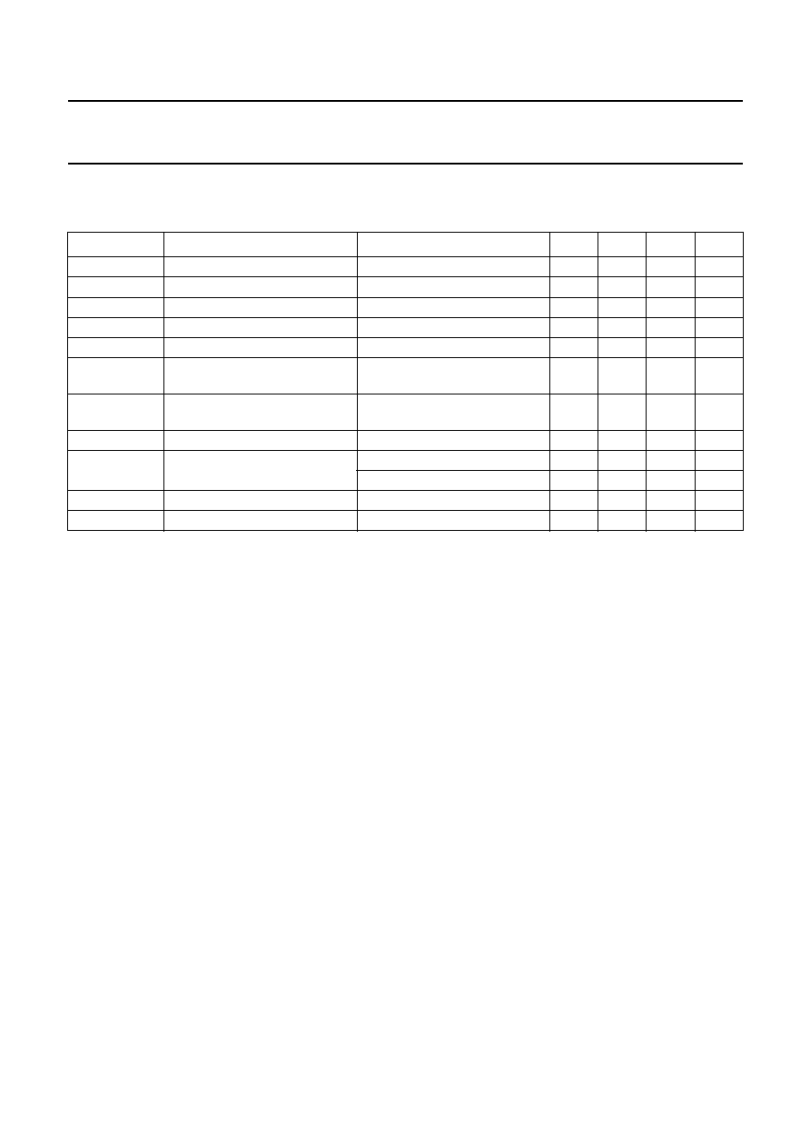
CHARACTERISTICS
Table 1
Bandwidth 5 to 200 MHz; T
mb
= 30
°
C; Z
S
= Z
L
= 75
Notes
1. f
p
= 83.25 MHz; V
p
= 50 dBmV;
f
q
= 109.25 MHz; V
q
= 50 dBmV;
measured at f
p
+ f
q
= 192.5 MHz.
2. Measured according to DIN45004B;
f
p
= 35.25 MHz; V
o
= V
p
;
f
q
= 42.25 MHz; V
q
= V
o
-
6 dB;
f
r
= 44.25 MHz; V
r
= V
o
-
6 dB;
measured at f
p
+ f
q
-
f
r
= 33.25 MHz.
3. Measured according to DIN45004B;
f
p
= 187.25 MHz; V
o
= V
p
;
f
q
= 194.25 MHz; V
q
= V
o
-
6 dB;
f
r
= 196.25 MHz; V
r
= V
o
-
6 dB;
measured at f
p
+ f
q
-
f
r
= 185.25 MHz.
4. The module normally operates at V
B
= +24 V, but is able to withstand supply transients up to +30 V.
SYMBOL
PARAMETER
CONDITIONS
MIN.
TYP.
MAX.
UNIT
G
p
power gain
f = 10 MHz
21.5
-
22.5
dB
SL
slope cable equivalent
f = 5 to 200 MHz
-
0.2
-
+0.5
dB
FL
flatness of frequency response
f = 5 to 200 MHz
-
-
±
0.2
dB
S
11
input return losses
f = 5 to 200 MHz
20
-
-
dB
S
22
output return losses
f = 5 to 200 MHz
20
-
-
dB
CTB
composite triple beat
22 channels flat; V
o
= 50 dBmV;
measured at 175.25 MHz
-
-
-
67
dB
X
mod
cross modulation
22 channels flat; V
o
= 50 dBmV;
measured at 55.25 MHz
-
-
-
60
dB
d
2
second order distortion
V
o
= 50 dBmV; note 1
-
-
-
67
dB
V
o
output voltage
d
im
=
-
60 dB; note 2
67
-
-
dBmV
d
im
=
-
60 dB; note 3
64
-
-
dBmV
F
noise figure
f = 200 MHz
-
-
5.5
dB
I
tot
total current consumption
DC value; V
B
= +24 V; note 4
-
215
230
mA

1997 Apr 15
4
Philips Semiconductors
Product specification
CATV amplifier module
BGY67
PACKAGE OUTLINE
Dimensions in mm.
(1) Screw 6-32 UNC-2A available on request.
(2) Leads gold plated.
Fig.2 SOT115J.
handbook, full pagewidth
1
7 8
20.8
max
4.2
M
0.25
9
0.51
0.38
(2)
(5.08)
2.54
UNC 6-32
(1)
25.4
12.7
27.2 max
3.8
max
8.8
min
9.2
max
8
13.8 max
0.25
2.54
2.4 max
44.8
max
38.1
4.15
3.85
MSA318 - 1
10.2
4.15
3.85
2 3
5

1997 Apr 15
5
Philips Semiconductors
Product specification
CATV amplifier module
BGY67
DEFINITIONS
LIFE SUPPORT APPLICATIONS
These products are not designed for use in life support appliances, devices, or systems where malfunction of these
products can reasonably be expected to result in personal injury. Philips customers using or selling these products for
use in such applications do so at their own risk and agree to fully indemnify Philips for any damages resulting from such
improper use or sale.
Data Sheet Status
Objective specification
This data sheet contains target or goal specifications for product development.
Preliminary specification
This data sheet contains preliminary data; supplementary data may be published later.
Product specification
This data sheet contains final product specifications.
Limiting values
Limiting values given are in accordance with the Absolute Maximum Rating System (IEC 134). Stress above one or
more of the limiting values may cause permanent damage to the device. These are stress ratings only and operation
of the device at these or at any other conditions above those given in the Characteristics sections of the specification
is not implied. Exposure to limiting values for extended periods may affect device reliability.
Application information
Where application information is given, it is advisory and does not form part of the specification.