1.
Product profile
1.1 General description
Silicon Monolithic Microwave Integrated Circuit (MMIC) wideband amplifier with internal
matching circuit in a 6-pin SOT363 SMD plastic package.
1.2 Features
s
Internally matched to 50
s
Good output match to 75
s
32 dB to 34 dB positive sloped gain for Low Noise Block (LNB) application
s
12.9 dBm saturated load power at 1 GHz
s
40 dB isolation
1.3 Applications
s
LNB Intermediate Frequency (IF) amplifiers
s
Cable systems
s
General purpose
1.4 Quick reference data
BGM1014
MMIC wideband amplifier
Rev. 01 -- 11 March 2005
Product data sheet
CAUTION
This device is sensitive to ElectroStatic Discharge (ESD). Therefore care should be taken
during transport and handling.
MSC895
Table 1:
Quick reference data
Symbol
Parameter
Conditions
Min
Typ
Max
Unit
V
S
DC supply voltage
RF input; AC coupled
-
5
6
V
I
S
DC supply current
17
21.0
25
mA
|
s
21
|
2
insertion power gain
f = 1 GHz
31.5
32.3
33.0
dB
NF
noise figure
f = 1 GHz
-
4.2
4.3
dB
P
L(sat)
saturated load power
f = 1 GHz
12.5
12.9
-
dBm

9397 750 14499
© Koninklijke Philips Electronics N.V. 2005. All rights reserved.
Product data sheet
Rev. 01 -- 11 March 2005
2 of 13
Philips Semiconductors
BGM1014
MMIC wideband amplifier
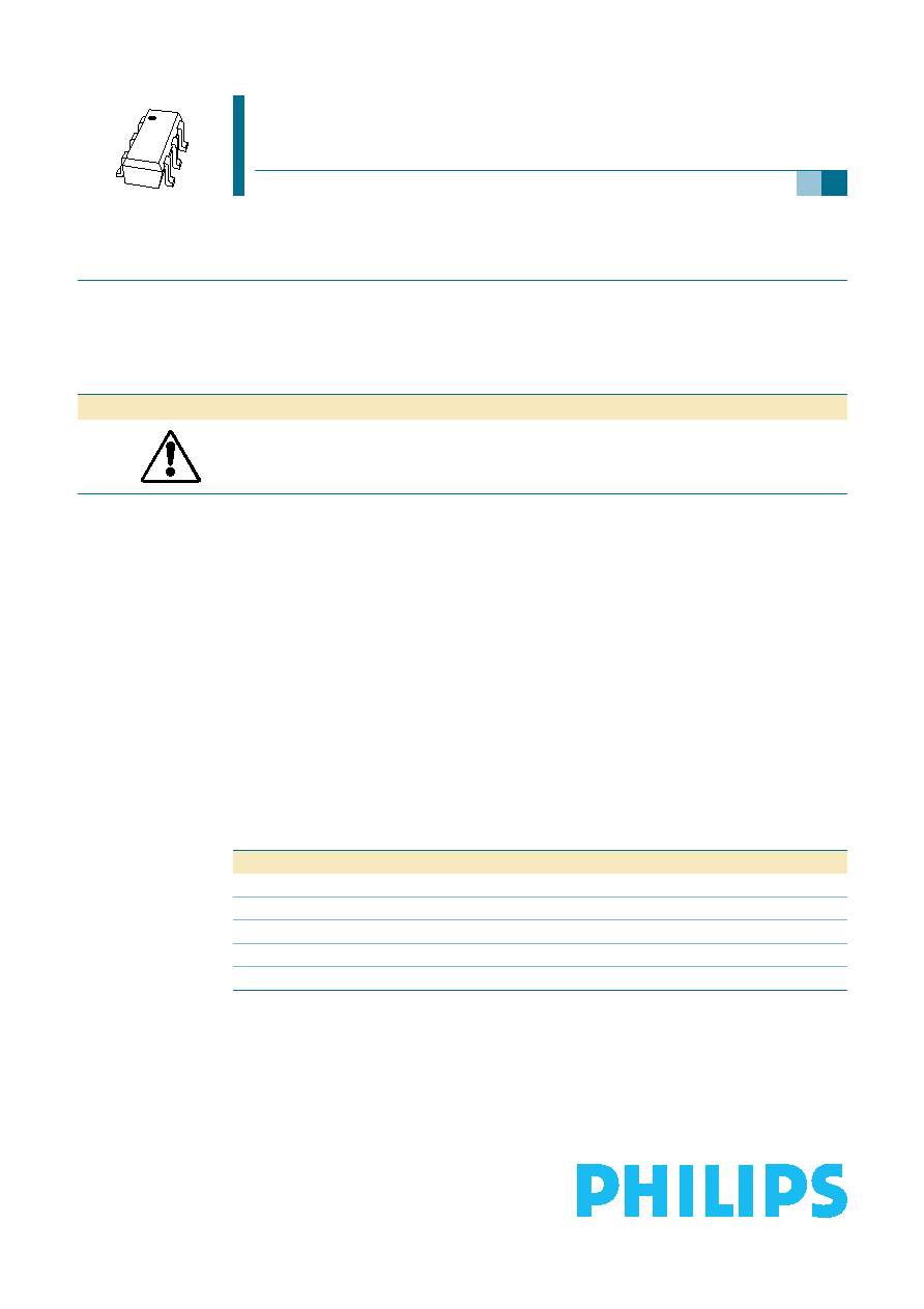
2.
Pinning information
3.
Ordering information
4.
Marking
5.
Limiting values
6.
Recommended operating conditions
Table 2:
Pinning
Pin
Description
Simplified outline
Symbol
1
V
S
2, 5
GND2
3
RF_OUT
4
GND1
6
RF_IN
1
3
2
4
5
6
sym062
1
6
4
2, 5
3
Table 3:
Ordering information
Type number
Package
Name
Description
Version
BGM1014
SC-88
plastic surface mounted package; 6 leads
SOT363
Table 4:
Marking
Type number
Marking code
BGM1014
C5-
Table 5:
Limiting values
In accordance with the Absolute Maximum Rating System (IEC 60134).
Symbol
Parameter
Conditions
Min
Max
Unit
V
S
DC supply voltage
RF input; AC coupled
-
6
V
I
S
supply current
-
30
mA
P
tot
total power dissipation
T
sp
90
°
C
-
200
mW
T
stg
storage temperature
-
65
+150
°
C
T
j
junction temperature
-
150
°
C
P
D
maximum drive power
-
-
10
dBm
Table 6:
Operating conditions
Symbol
Parameter
Conditions
Min
Typ
Max
Unit
V
S
DC supply voltage
4.5
5.0
5.5
V
T
amb
ambient temperature
-
40
+25
+85
°
C

9397 750 14499
© Koninklijke Philips Electronics N.V. 2005. All rights reserved.
Product data sheet
Rev. 01 -- 11 March 2005
3 of 13
Philips Semiconductors
BGM1014
MMIC wideband amplifier
7.
Thermal characteristics
8.
Characteristics
Table 7:
Thermal characteristics
Symbol
Parameter
Conditions
Typ
Unit
R
th(j-sp)
thermal resistance from junction to solder point
P
tot
= 200 mW; T
sp
90
°
C
300
K/W
Table 8:
Characteristics
V
S
= 5 V; I
S
= 21.1 mA; T
j
= 25
°
C; measured on demo board; unless otherwise specified.
Symbol Parameter
Conditions
Min
Typ
Max
Unit
V
S
DC supply voltage
RF input; AC coupled
-
5
6
V
I
S
supply current
17
21.0
25
mA
|
s
21
|
2
insertion power gain
see
Figure 4
f = 100 MHz
29.0
30.0
31.0
dB
f = 1 GHz
31.5
32.3
33.0
dB
f = 1.8 GHz
34.0
35.2
36.5
dB
f = 2.2 GHz
33.0
34.1
35.5
dB
f = 2.6 GHz
29.0
30.5
32.0
dB
f = 3 GHz
25.0
26.4
28.0
dB
|
s
11
|
2
input return loss
f = 1 GHz
11
12.2
-
dB
f = 2.2 GHz
7.5
8.8
-
dB
|
s
22
|
2
output return loss
Z
L
= 50
f = 1 GHz
15
18.9
-
dB
f = 2.2 GHz
12
16.7
-
dB
Z
L
= 75
f = 1 GHz
12
16.8
-
dB
f = 2.2 GHz
12
17.7
-
dB
|
s
12
|
2
isolation
see
Figure 3
f = 1 GHz
40
42
-
dB
f = 2.2 GHz
35
37
-
dB
NF
noise figure
see
Figure 7
f = 1 GHz
-
4.2
4.3
dB
f = 2.2 GHz
-
4.1
4.3
dB
B
bandwidth
3 dB below flat gain at f = 1 GHz
-
2.5
-
GHz
K
stability factor
see
Figure 8
f = 1 GHz
1.5
1.6
-
f = 2.2 GHz
0.9
1.0
-
P
L(sat)
saturated load power
f = 1 GHz
12.5
12.9
-
dBm
f = 2.2 GHz
8.8
9.3
-
dBm
P
L(1dB)
load power at 1 dB gain
compression
f = 1 GHz
10.5
11.2
-
dBm
f = 2.2 GHz
5.0
5.7
-
dBm

9397 750 14499
© Koninklijke Philips Electronics N.V. 2005. All rights reserved.
Product data sheet
Rev. 01 -- 11 March 2005
4 of 13
Philips Semiconductors
BGM1014
MMIC wideband amplifier
IP3
in
input third order intercept point
f = 1 GHz
-
13
-
11.8
-
dBm
f = 2.2 GHz
-
21
-
19
-
dBm
IP3
out
output third order intercept point f = 1 GHz
19.5
20.5
-
dBm
f = 2.2 GHz
14
15.1
-
dBm
IM2
second order intermodulation
distortion
f
0
= 1 GHz; P
L
=
-
10 dBm
36
37
-
dBc
f
0
= 1 GHz; P
L
=
-
5 dBm
33
34
-
dBc
Table 8:
Characteristics
...continued
V
S
= 5 V; I
S
= 21.1 mA; T
j
= 25
°
C; measured on demo board; unless otherwise specified.
Symbol Parameter
Conditions
Min
Typ
Max
Unit
I
S
= 21.1 mA; V
S
= 5 V; P
D
=
-
35 dBm; Z
o
= 50
Fig 1.
Input reflection coefficient (s
11
); typical values
001aac489
90
°
-
90
°
5
0.5
0.2
+
0.2
0
+
2
+
5
-
5
-
2
-
0.2
+
0.5
-
0.5
+
1
-
1
2
1
10
0
0.2
0.6
0.4
0.8
1.0
1.0
-
45
°
-
135
°
45
°
135
°
180
°
0
°
3GHz
100MHz

9397 750 14499
© Koninklijke Philips Electronics N.V. 2005. All rights reserved.
Product data sheet
Rev. 01 -- 11 March 2005
5 of 13
Philips Semiconductors
BGM1014
MMIC wideband amplifier
I
S
= 21.1 mA; V
S
= 5 V; P
D
=
-
35 dBm; Z
o
= 50
Fig 2.
Output reflection coefficient (s
22
); typical values
I
S
= 21.1 mA; V
S
= 5 V; P
D
=
-
35 dBm; Z
o
= 50
P
D
=
-
35 dBm; Z
o
= 50
(1) I
S
= 25.6 mA; V
S
= 5.5 V
(2) I
S
= 21.5 mA; V
S
= 5 V
(3) I
S
= 16.6 mA; V
S
= 4.5 V
Fig 3.
Isolation (
|
s
12
|
2
) as a function of frequency;
typical values
Fig 4.
Insertion gain (
|
s
21
|
2
) as a function of frequency;
typical values
001aac490
90
°
-
90
°
5
0.5
0.2
+
0.2
0
+
2
+
5
-
5
-
2
-
0.2
+
0.5
-
0.5
+
1
-
1
2
1
10
0
0.2
0.6
0.4
0.8
1.0
1.0
-
45
°
-
135
°
45
°
135
°
180
°
0
°
3GHz
100MHz
001aac491
f (MHz)
0
3000
2000
1000
-
30
-
20
-
40
-
10
0
s
12
2
(dB)
-
50
001aac492
f (MHz)
0
3000
2000
1000
30
20
40
50
10
s
21
2
(dB)
(1)
(2)
(3)