
DATA SHEET
Product specification
Supersedes data of October 1992
File under discrete semiconductors, SC14
1995 Sep 18
DISCRETE SEMICONDUCTORS
BFR92AW
NPN 5 GHz wideband transistor
1995 Sep 18
2
Philips Semiconductors
Product specification
NPN 5 GHz wideband transistor
BFR92AW
FEATURES
·
High power gain
·
Gold metallization ensures
excellent reliability
·
SOT323 (S-mini) package.
APPLICATIONS
It is designed for use in RF amplifiers,
mixers and oscillators with signal
frequencies up to 1 GHz.
DESCRIPTION
Silicon NPN transistor encapsulated
in a plastic SOT323 (S-mini) package.
The BFR92AW uses the same crystal
as the SOT23 version, BFR92A.
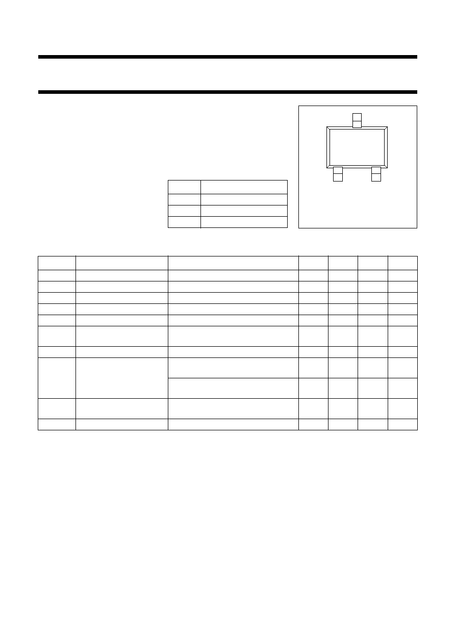
PINNING
PIN
DESCRIPTION
1
base
2
emitter
3
collector
Marking code: P2.
Fig.1 SOT323
handbook, 2 columns
3
1
2
MBC870
Top view
QUICK REFERENCE DATA
Note
1. T
s
is the temperature at the soldering point of the collector pin.
SYMBOL
PARAMETER
CONDITIONS
MIN.
TYP.
MAX.
UNIT
V
CBO
collector-base voltage
open emitter
-
-
20
V
V
CEO
collector-emitter voltage
open base
-
-
15
V
I
C
collector current (DC)
-
-
25
mA
P
tot
total power dissipation
up to T
s
= 93
°
C; note 1
-
-
300
mW
h
FE
current gain
I
C
= 15 mA; V
CE
= 10 V
40
90
-
C
re
feedback capacitance
I
C
= 0; V
CE
= 10 V; f = 1 MHz;
T
amb
= 25
°
C
-
0.35
-
pF
f
T
transition frequency
I
C
= 15 mA; V
CE
= 10 V; f = 500 MHz
3.5
5
-
GHz
G
UM
maximum unilateral power
gain
I
C
= 15 mA; V
CE
= 10 V; f = 1 GHz;
T
amb
= 25
°
C
-
14
-
dB
I
C
= 15 mA; V
CE
= 10 V; f = 2 GHz;
T
amb
= 25
°
C
-
8
-
dB
F
noise figure
I
C
= 5 mA; V
CE
= 10 V; f = 1 GHz;
s
=
opt
-
2
-
dB
T
j
junction temperature
-
-
150
°
C
1995 Sep 18
3
Philips Semiconductors
Product specification
NPN 5 GHz wideband transistor
BFR92AW
LIMITING VALUES
In accordance with the Absolute Maximum System (IEC 134).
THERMAL CHARACTERISTICS
Note to the Limiting values and Thermal characteristics
1. T
s
is the temperature at the soldering point of the collector pin.
SYMBOL
PARAMETER
CONDITIONS
MIN.
MAX.
UNIT
V
CBO
collector-base voltage
open emitter
-
20
V
V
CEO
collector-emitter voltage
open base
-
15
V
V
EBO
emitter-base voltage
open collector
-
2
V
I
C
collector current (DC)
-
25
mA
P
tot
total power dissipation
up to T
s
= 93
°
C; see Fig.2; note 1
-
300
mW
T
stg
storage temperature
-
65
+150
°
C
T
j
junction temperature
-
150
°
C
SYMBOL
PARAMETER
CONDITIONS
VALUE
UNIT
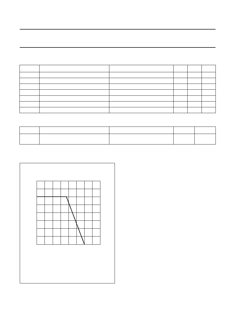
R
th j-s
thermal resistance from junction to
soldering point
up to T
s
= 93
°
C; note 1
190
K/W
Fig.2 Power derating curve
0
50
100
200
200
0
MLB540
150
T ( C)
o
s
Ptot
(mW)
300
400
100
1995 Sep 18
4
Philips Semiconductors
Product specification
NPN 5 GHz wideband transistor
BFR92AW
CHARACTERISTICS
T
j
= 25
°
C (unless otherwise specified).
Note
1. G
UM
is the maximum unilateral power gain, assuming s
12
is zero and
SYMBOL
PARAMETER
CONDITIONS
MIN.
TYP.
MAX.
UNIT
I
CBO
collector leakage current
I
E
= 0; V
CB
= 10 V
-
-
50
nA
h
FE
DC current gain
I
C
= 15 mA; V
CE
= 10 V
40
90
-
C
c
collector capacitance
I
E
= i
e
= 0; V
CB
= 10 V; f = 1 MHz
-
0.6
-
pF
C
e
emitter capacitance
I
C
= i
c
= 0; V
EB
= 0.5 V; f = 1 MHz
-
0.9
-
pF
C
re
feedback capacitance
I
C
= 0; V
CE
= 10 V; f = 1 MHz
-
0.35
-
pF
f
T
transition frequency
I
C
= 15 mA; V
CE
= 10 V; f = 500 MHz
3.5
5
-
GHz
G
UM
maximum unilateral power
gain; note 1
I
C
= 15 mA; V
CE
= 10 V;
f = 1 GHz; T
amb
= 25
°
C
-
14
-
dB
I
C
= 15 mA; V
CE
= 10 V;
f = 2 GHz; T
amb
= 25
°
C
-
8
-
dB
F
noise figure
I
C
= 5 mA; V
CE
= 10 V;
f = 1 GHz;
s
=
opt
-
2
-
dB
I
C
= 5 mA; V
CE
= 10 V;
f = 2 GHz;
s
=
opt
-
3
-
dB
G
UM
10
s
21
2
1
s
11
2
(
)
1
s
22
2
(
)
------------------------------------------------------------ dB.
log
=
1995 Sep 18
5
Philips Semiconductors
Product specification
NPN 5 GHz wideband transistor
BFR92AW
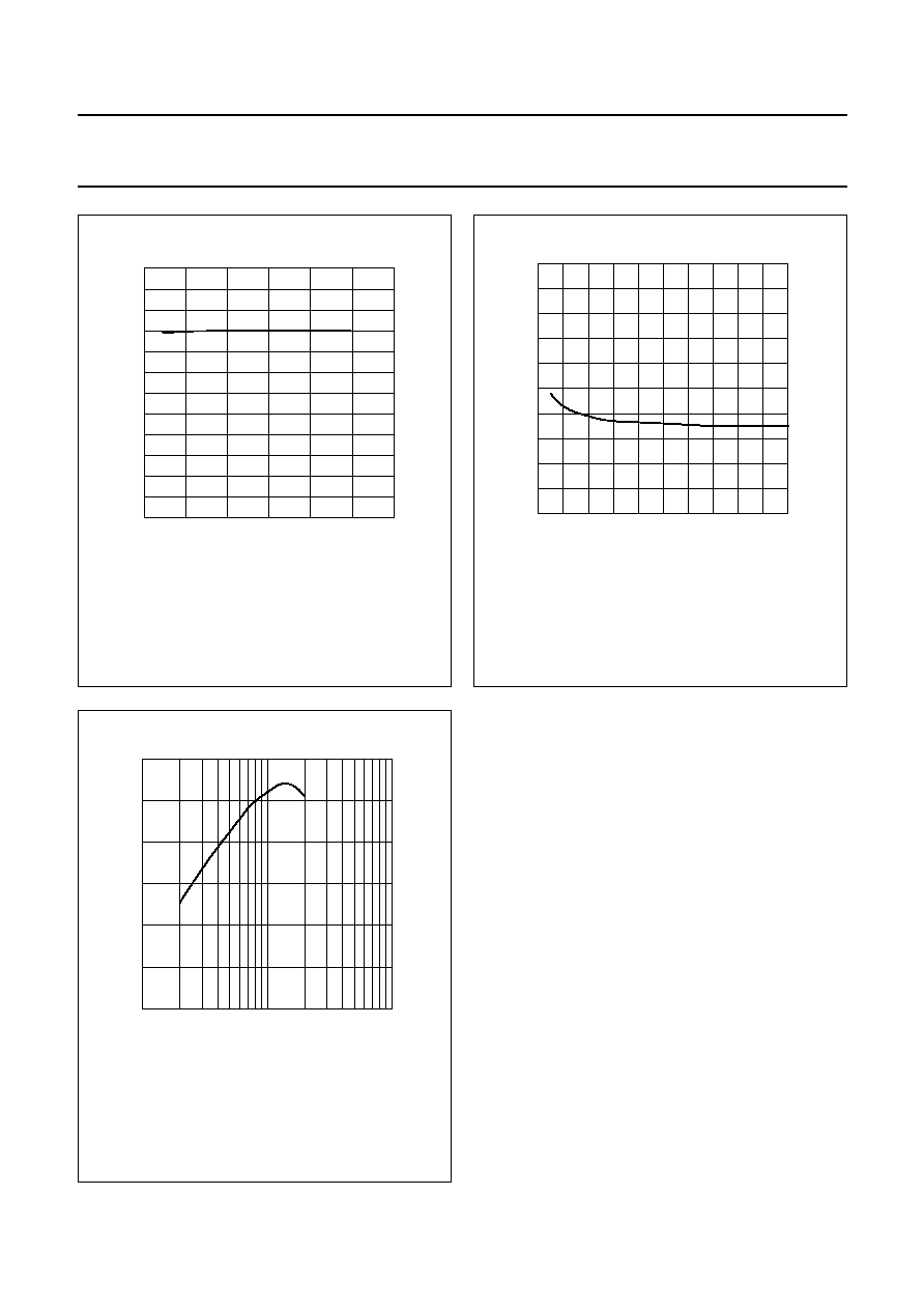
Fig.3
DC current gain as a function of collector
current; typical values.
V
CE
= 10 V.
handbook, halfpage
0
10
20
30
120
0
40
80
MCD074
h FE
I (mA)
C
Fig.4
Feedback capacitance as a function of
collector-base voltage; typical values.
I
C
= 0; f = 1 MHz.
0
1.0
0
20
MGC883
4
8
V (V)
CB
C re
(pF)
0.8
0.6
0.4
0.2
12
16
Fig.5
Transition frequency as a function of
collector current; typical values.
V
CE
= 5 V; f = 500 MHz; T
amb
= 25
°
C.
handbook, halfpage
4
2
0
MGC884
10
1
6
f
T
(GHz)
I (mA)
C
10
2