1999 Apr 26
2
Philips Semiconductors
Product specification
PNP general purpose double transistor
BC857BS
FEATURES
·
Low collector capacitance
·
Low collector-emitter saturation voltage
·
Closely matched current gain
·
Reduces number of components and boardspace
·
No mutual interference between the transistors.
APPLICATIONS
·
General purpose switching and amplification.
DESCRIPTION
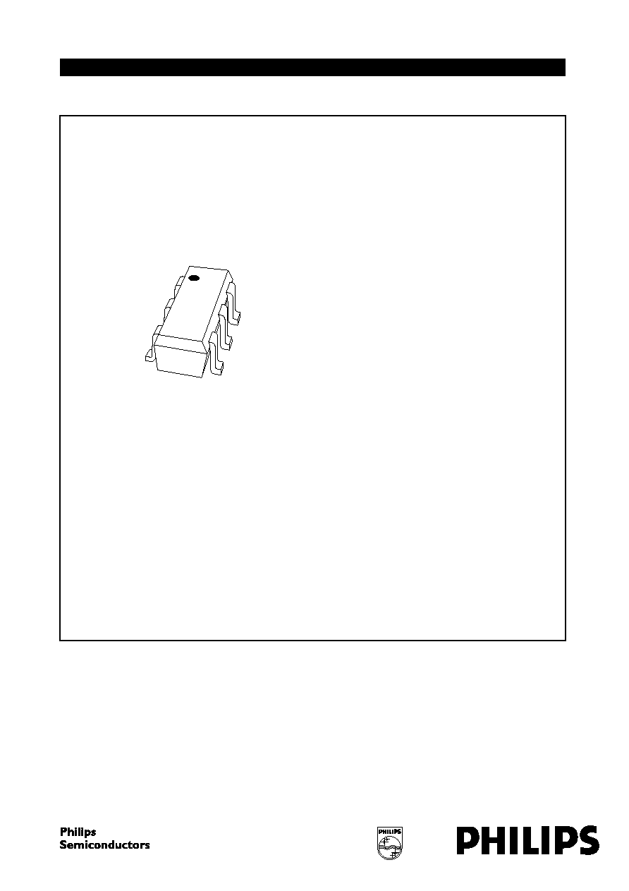
PNP double transistor in an SC-88; SOT363 plastic
package. NPN complement: BC847BS.
MARKING
TYPE NUMBER
MARKING CODE
BC857BS
3Ft
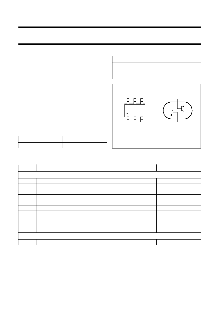
PINNING
PIN
DESCRIPTION
1, 4
emitter
TR1; TR2
2, 5
base
TR1; TR2
6, 3
collector
TR1; TR2
Fig.1
Simplified outline (SC-88; SOT363)
and symbol.
handbook, halfpage
1
3
2
4
5
6
Top view
MAM339
1
3
2
TR1
TR2
6
4
5
LIMITING VALUES
In accordance with the Absolute Maximum Rating System (IEC 134).
Note
1. Device mounted on an FR4 printed-circuit board.
SYMBOL
PARAMETER
CONDITIONS
MIN.
MAX.
UNIT
Per transistor
V
CBO
collector-base voltage
open emitter
-
-
50
V
V
CEO
collector-emitter voltage
open base
-
-
45
V
V
EBO
emitter-base voltage
open collector
-
-
5
V
I
C
collector current (DC)
-
-
100
mA
I
CM
peak collector current
-
-
200
mA
I
BM
peak base current
-
-
200
mA
P
tot
total power dissipation
T
amb
25
°
C
-
200
mW
T
stg
storage temperature
-
65
+150
°
C
T
j
junction temperature
-
150
°
C
T
amb
operating ambient temperature
-
65
+150
°
C
Per device
P
tot
total power dissipation
T
amb
25
°
C; note 1
-
300
mW
1999 Apr 26
3
Philips Semiconductors
Product specification
PNP general purpose double transistor
BC857BS
THERMAL CHARACTERISTICS
Note
1. Device mounted on an FR4 printed-circuit board.
CHARACTERISTICS
T
amb
= 25
°
C unless otherwise specified.
Note
1. Pulse test: t
p
300
µ
s;
0.02.
SYMBOL
PARAMETER
CONDITIONS
VALUE
UNIT
Per device
R
th j-a
thermal resistance from junction to ambient
note 1
416
K/W
SYMBOL
PARAMETER
CONDITIONS
MIN.
TYP.
MAX.
UNIT
Per transistor
I
CBO
collector cut-off current
I
E
= 0; V
CB
=
-
30 V
-
-
-
15
nA
I
E
= 0; V
CB
=
-
30 V; T
j
= 150
°
C
-
-
-
5
µ
A
I
EBO
emitter cut-off current
I
C
= 0; V
EB
=
-
5 V
-
-
-
100
nA
h
FE
DC current gain
I
C
=
-
2 mA; V
CE
=
-
5 V
200
-
450
V
CEsat
collector-emitter saturation
voltage
I
C
=
-
10 mA; I
B
=
-
0.5 mA
-
-
-
100
mV
I
C
=
-
100 mA; I
B
=
-
5 mA; note 1
-
-
-
400
mV
V
BEsat
base-emitter saturation voltage
I
C
=
-
10 mA; I
B
=
-
0.5 mA
-
-
755
-
mV
V
BE
base-emitter voltage
I
C
=
-
2 mA; V
CE
=
-
5 V
-
600
-
655
-
750
mV
C
c
collector capacitance
I
E
= i
e
= 0; V
CB
=
-
10 V; f = 1 MHz
-
-
2.2
pF
C
e
emitter capacitance
I
C
= i
c
= 0; V
EB
=
-
500 mV; f = 1 MHz
-
10
-
pF
f
T
transition frequency
I
C
=
-
10 mA; V
CE
=
-
5 V; f = 100 MHz
100
-
-
MHz
1999 Apr 26
5
Philips Semiconductors
Product specification
PNP general purpose double transistor
BC857BS
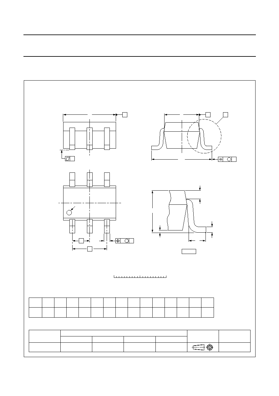
PACKAGE OUTLINE
REFERENCES
OUTLINE
VERSION
EUROPEAN
PROJECTION
ISSUE DATE
IEC
JEDEC
EIAJ
SOT363
SC-88
w
B
M
bp
D
e1
e
pin 1
index
A
A1
Lp
Q
detail X
HE
E
v
M
A
A
B
y
0
1
2 mm
scale
c
X
1
3
2
4
5
6
Plastic surface mounted package; 6 leads
SOT363
UNIT
A1
max
bp
c
D
E
e
1
HE
Lp
Q
y
w
v
mm
0.1
0.30
0.20
2.2
1.8
0.25
0.10
1.35
1.15
0.65
e
1.3
2.2
2.0
0.2
0.1
0.2
DIMENSIONS (mm are the original dimensions)
0.45
0.15
0.25
0.15
A
1.1
0.8
97-02-28