1999 Apr 12
2
Philips Semiconductors
Product specification
NPN general purpose transistors
BC849W; BC850W
FEATURES
·
Low current (max. 100 mA)
·
Low voltage (max. 45 V).
APPLICATIONS
·
Low noise stages in tape recorders, hi-fi amplifiers and
other audio-frequency equipment.
DESCRIPTION
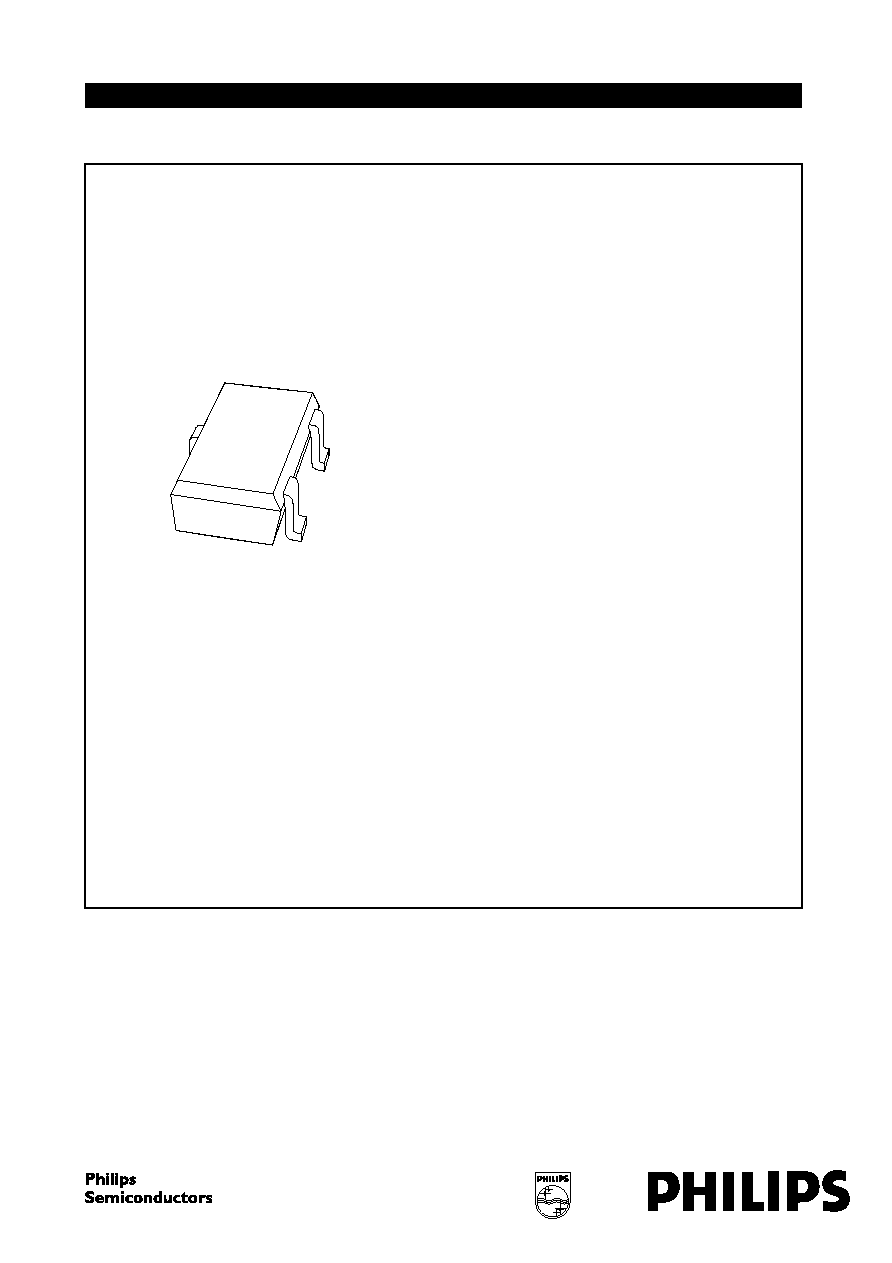
NPN transistor in a SOT323 plastic package.
PNP complements: BC859W and BC860W.
MARKING
Note
1.
= - : Made in Hong Kong.
= t : Made in Malaysia.
TYPE
NUMBER
MARKING
CODE
(1)
TYPE
NUMBER
MARKING
CODE
(1)
BC849BW
2B
BC850BW
2F
BC849CW
2C
BC850CW
2G
PINNING
PIN
DESCRIPTION
1
base
2
emitter
3
collector
Fig.1
Simplified outline (SOT323) and symbol.
handbook, halfpage
2
3
1
MAM062
3
2
1
Top view
LIMITING VALUES
In accordance with the Absolute Maximum Rating System (IEC 134).
Note
1. Transistor mounted on an FR4 printed-circuit board.
SYMBOL
PARAMETER
CONDITIONS
MIN.
MAX.
UNIT
V
CBO
collector-base voltage
open emitter
BC849W
-
30
V
BC850W
-
50
V
V
CEO
collector-emitter voltage
open base
BC849W
-
30
V
BC850W
-
45
V
V
EBO
emitter-base voltage
open collector
-
5
V
I
C
collector current (DC)
-
100
mA
I
CM
peak collector current
-
200
mA
I
BM
peak base current
-
200
mA
P
tot
total power dissipation
T
amb
25
°
C; note 1
-
200
mW
T
stg
storage temperature
-
65
+150
°
C
T
j
junction temperature
-
150
°
C
T
amb
operating ambient temperature
-
65
+150
°
C
1999 Apr 12
3
Philips Semiconductors
Product specification
NPN general purpose transistors
BC849W; BC850W
THERMAL CHARACTERISTICS
Note
1. Transistor mounted on an FR4 printed-circuit board.
CHARACTERISTICS
T
amb
= 25
°
C unless otherwise specified.
Note
1. Pulse test: t
p
300
µ
s;
0.02.
SYMBOL
PARAMETER
CONDITIONS
VALUE
UNIT
R
th j-a
thermal resistance from junction to ambient
note 1
625
K/W
SYMBOL
PARAMETER
CONDITIONS
MIN.
TYP.
MAX.
UNIT
I
CBO
collector cut-off current
I
E
= 0; V
CB
= 30 V
-
-
15
nA
I
E
= 0; V
CB
= 30 V; T
j
= 150
°
C
-
-
5
µ
A
I
EBO
emitter cut-off current
I
C
= 0; V
EB
= 5 V
-
-
100
nA
h
FE
DC current gain
I
C
= 2 mA; V
CE
= 5 V; see Figs 2 and 3
BC849BW; BC850BW
200
-
450
BC849CW; BC850CW
420
-
800
V
CEsat
collector-emitter saturation
voltage
I
C
= 10 mA; I
B
= 0.5 mA
-
-
250
mV
I
C
= 100 mA; I
B
= 5 mA; note 1
-
-
600
mV
V
BE
base-emitter voltage
I
C
= 2 mA; V
CE
= 5 V
580
-
700
mV
I
C
= 10 mA; V
CE
= 5 V
-
-
770
mV
C
c
collector capacitance
I
E
= i
e
= 0; V
CB
= 10 V; f = 1 MHz
-
-
3
pF
C
e
emitter capacitance
I
C
= i
c
= 0; V
EB
= 500 mV; f = 1 MHz
-
11
-
pF
f
T
transition frequency
I
C
= 10 mA; V
CE
= 5 V; f = 100 MHz
100
-
-
MHz
F
noise figure
I
C
= 200
µ
A; V
CE
= 5 V; R
S
= 2 k
;
f = 10 Hz to 15.7 kHz
-
-
4
dB
I
C
= 200
µ
A; V
CE
= 5 V; R
S
= 2 k
;
f = 1 kHz; B = 200 Hz
-
-
4
dB

1999 Apr 12
4
Philips Semiconductors
Product specification
NPN general purpose transistors
BC849W; BC850W
Fig.2 DC current gain; typical values.
handbook, full pagewidth
0
300
100
200
MBH724
10
-
2
10
-
1
hFE
1
IC (mA)
10
10
3
10
2
VCE = 5 V
BC849BW; BC850BW.
Fig.3 DC current gain; typical values.
handbook, full pagewidth
0
600
200
400
MBH725
10
-
2
10
-
1
hFE
1
IC (mA)
10
10
3
10
2
VCE = 5 V
BC849CW; BC850CW.
1999 Apr 12
5
Philips Semiconductors
Product specification
NPN general purpose transistors
BC849W; BC850W
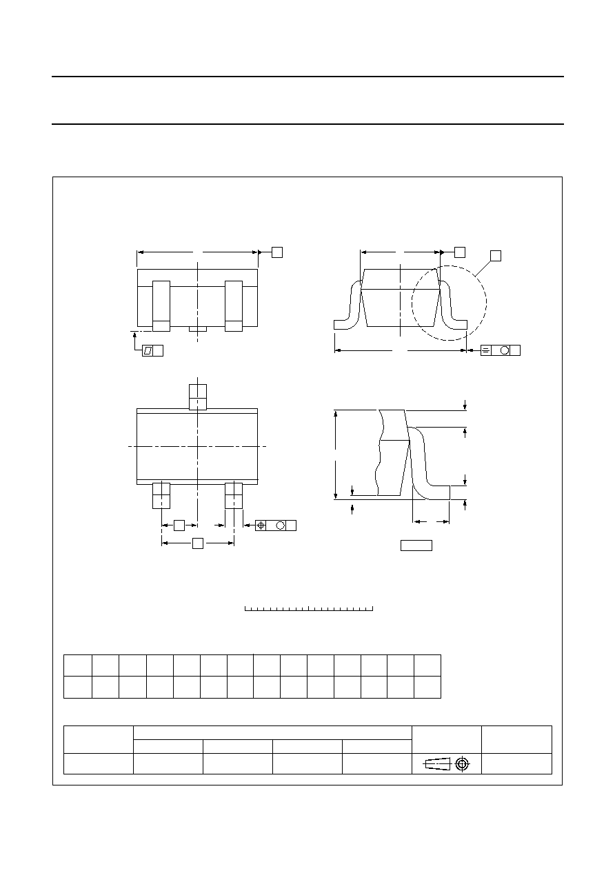
PACKAGE OUTLINE
UNIT
A1
max
bp
c
D
E
e1
HE
Lp
Q
w
v
REFERENCES
OUTLINE
VERSION
EUROPEAN
PROJECTION
ISSUE DATE
IEC
JEDEC
EIAJ
mm
0.1
1.1
0.8
0.4
0.3
0.25
0.10
2.2
1.8
1.35
1.15
0.65
e
1.3
2.2
2.0
0.23
0.13
0.2
0.2
DIMENSIONS (mm are the original dimensions)
0.45
0.15
SOT323
SC-70
w
M
bp
D
e1
e
A
B
A1
Lp
Q
detail X
c
HE
E
v
M
A
A
B
y
0
1
2 mm
scale
A
X
1
2
3
Plastic surface mounted package; 3 leads
SOT323
97-02-28