DATA SHEET
Product specification
Supersedes data of 1998 Jan 21
1998 Oct 30
DISCRETE SEMICONDUCTORS
BAT120 series
Schottky barrier double diodes
halfpage
M3D087
1998 Oct 30
2
Philips Semiconductors
Product specification
Schottky barrier double diodes
BAT120 series
FEATURES
·
Low switching losses
·
Capability of absorbing very high
surge current
·
Fast recovery time
·
Guard ring protected
·
Plastic SMD package.
APPLICATIONS
·
Low power switched-mode power
supplies
·
Rectification
·
Polarity protection.
DESCRIPTION
Planar Schottky barrier double diodes
encapsulated in a SOT223 plastic
SMD package
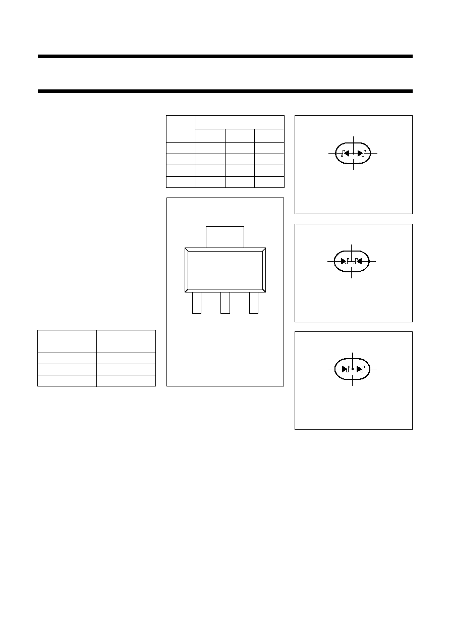
PINNING
PIN
BAT120
A
C
S
1
k
1
a
1
a
1
2
n.c.
n.c.
n.c.
3
k
2
a
2
k
2
4
a
1
, a
2
k
1
, k
2
k
1
, a
2
Fig.1
Simplified outline
(SOT223) and pin
configuration.
age
4
1
2
3
MSB002 - 1
Top view
Fig.2
BAT120A diode
configuration (symbol).
page
MGL171
1
3
2 n.c.
4
Fig.3
BAT120C diode
configuration (symbol).
page
MGL172
1
3
2 n.c.
4
Fig.4
BAT120S diode
configuration (symbol).
page
MGL173
1
3
4
2 n.c.
MARKING
TYPE NUMBER
MARKING
CODE
BAT120A
AT120A
BAT120C
AT120C
BAT120S
AT120S

1998 Oct 30
3
Philips Semiconductors
Product specification
Schottky barrier double diodes
BAT120 series
LIMITING VALUES
In accordance with the Absolute Maximum Rating System (IEC 134).
ELECTRICAL CHARACTERISTICS
T
amb
= 25
°
C unless otherwise specified.
Note
1. Pulse test: t
p
= 300
µ
s;
= 0.02.
THERMAL CHARACTERISTICS
Note
1. Refer to SOT223 standard mounting conditions.
SYMBOL
PARAMETER
CONDITIONS
MIN.
MAX.
UNIT
Per diode
V
R
continuous reverse voltage
-
25
V
I
F
continuous forward current
-
1
A
I
FSM
non-repetitive peak forward current
t
p
<
10 ms; half sinewave;
JEDEC method
-
10
A
I
RSM
non-repetitive peak reverse current
t
p
= 100
µ
s
-
0.5
A
T
stg
storage temperature
-
65
+150
°
C
T
j
junction temperature
-
125
°
C
T
amb
operating ambient temperature
-
65
+125
°
C
SYMBOL
PARAMETER
CONDITIONS
TYP.
MAX.
UNIT
Per diode
V
F
forward voltage
see Fig.5
I
F
= 100 mA
260
300
mV
I
F
= 1 A
400
450
mV
I
R
reverse current
V
R
= 20 V; note 1; see Fig.6
80
500
µ
A
V
R
= 25 V; note 1; see Fig.6
-
1
mA
V
R
= 20 V; T
j
= 100
°
C; note 1
-
10
mA
C
d
diode capacitance
f = 1 MHz; V
R
= 4 V; see Fig.7
100
-
pF
SYMBOL
PARAMETER
CONDITIONS
VALUE
UNIT
R
th j-a
thermal resistance from junction to ambient
note 1
100
K/W
1998 Oct 30
4
Philips Semiconductors
Product specification
Schottky barrier double diodes
BAT120 series
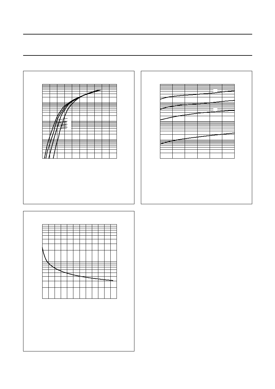
GRAPHICAL DATA
(1) T
amb
= 125
°
C.
(2) T
amb
= 100
°
C.
(3) T
amb
= 75
°
C.
(4) T
amb
= 25
°
C.
Fig.5
Forward current as a function of forward
voltage; typical values.
handbook, halfpage
1.0
VF (V)
IF
(mA)
0
0.2
0.4
0.6
0.8
10
4
10
3
10
2
10
1
MBK572
(1)
(2)
(3)
(4)
(1) T
amb
= 125
°
C.
(2) T
amb
= 100
°
C.
(3) T
amb
= 75
°
C.
(4) T
amb
= 25
°
C.
Fig.6
Reverse current as a function of reverse
voltage; typical values.
handbook, halfpage
30
VR (V)
IR
(mA)
0
10
20
10
4
10
3
10
2
10
1
MBK573
(1)
(2)
(3)
(4)
Fig.7
Diode capacitance as a function of reverse
voltage; typical values.
f = 1 MHz; T
amb
= 25
°
C.
handbook, halfpage
30
VR (V)
Cd
(pF)
0
10
20
10
3
10
2
10
MBK571
1998 Oct 30
5
Philips Semiconductors
Product specification
Schottky barrier double diodes
BAT120 series
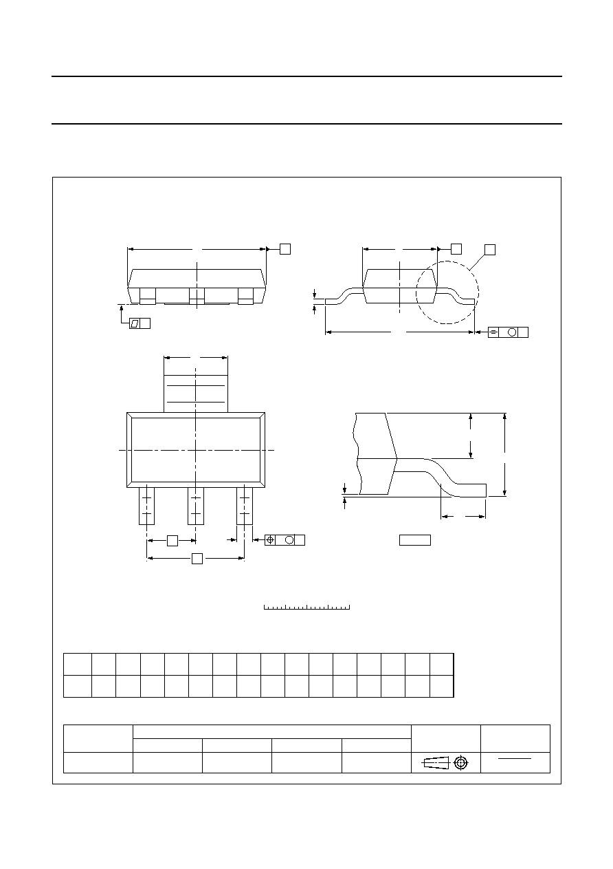
PACKAGE OUTLINE
UNIT
A
1
b
p
c
D
E
e
1
H
E
L
p
Q
y
w
v
REFERENCES
OUTLINE
VERSION
EUROPEAN
PROJECTION
ISSUE DATE
IEC
JEDEC
EIAJ
mm
0.10
0.01
1.8
1.5
0.80
0.60
b
1
3.1
2.9
0.32
0.22
6.7
6.3
3.7
3.3
2.3
e
4.6
7.3
6.7
1.1
0.7
0.95
0.85
0.1
0.1
0.2
DIMENSIONS (mm are the original dimensions)
SOT223
96-11-11
97-02-28
w
M
b
p
D
b
1
e
1
e
A
A
1
L
p
Q
detail X
H
E
E
v
M
A
A
B
B
c
y
0
2
4 mm
scale
A
X
1
3
2
4
Plastic surface mounted package; collector pad for good heat transfer; 4 leads
SOT223