Philips Semiconductors
Product specification
74LVT16500A
3.3V 18-bit universal bus transceiver (3-State)
2
1998 Feb 19
853-1789 18989
FEATURES
À
18-bit bidirectional bus interface
À
3-State buffers
À
Output capability: +64mA/-32mA
À
TTL input and output switching levels
À
Input and output interface capability to systems at 5V supply
À
Bus-hold data inputs eliminate the need for external pull-up
resistors to hold unused inputs
À
Live insertion/extraction permitted
À
Power-up reset
À
Power-up 3-State
À
No bus current loading when output is tied to 5V bus
À
Negative edge-triggered clock inputs
À
Latch-up protection exceeds 500mA per JEDEC JC40.2 Std 17
À
ESD protection exceeds 2000V per MIL STD 883 Method 3015
and 200V per Machine Model
DESCRIPTION
The 74LVT16500A is a high-performance BiCMOS product
designed for V
CC
operation at 3.3V.
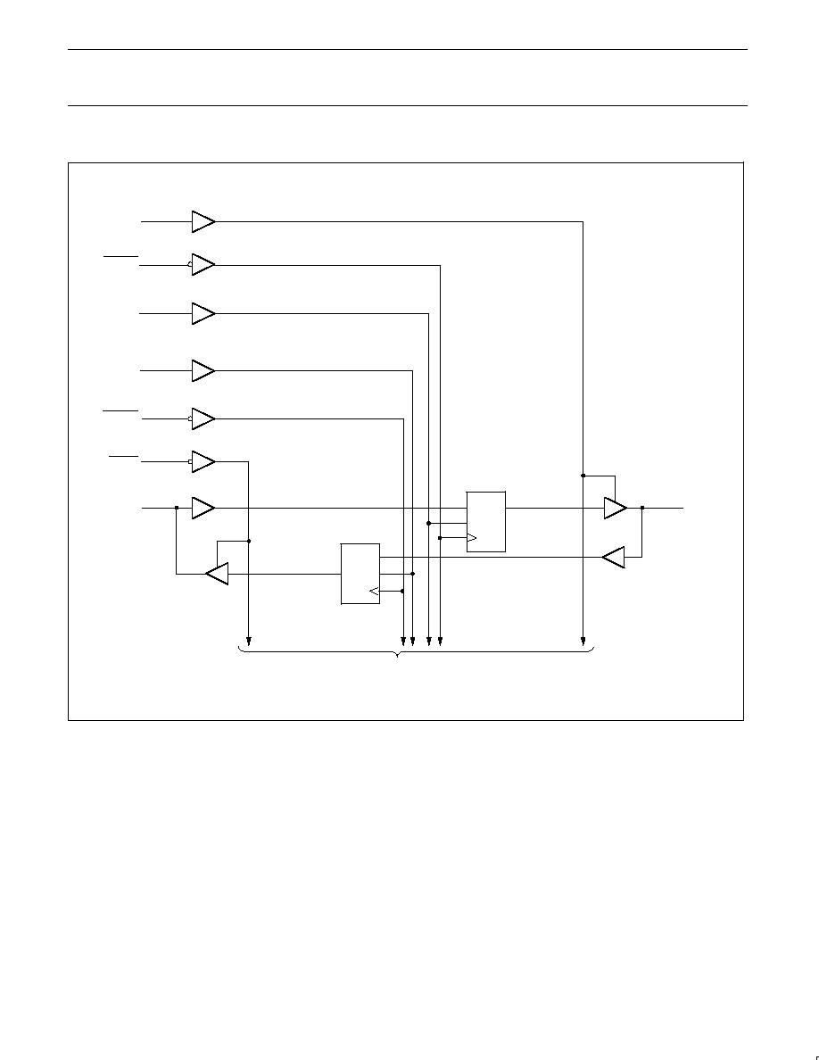
This device is an 18-bit universal transceiver featuring non-inverting
3-State bus compatible outputs in both send and receive directions.
Data flow in each direction is controlled by output enable (OEAB and
OEBA), latch enable (LEAB and LEBA), and clock (CPAB and
CPBA) inputs. For A-to-B data flow, the device operates in the
transparent mode when LEAB is High. When LEAB is Low, the A
data is latched if CPAB is held at a High or Low logic level. If LEAB
is Low, the A-bus data is stored in the latch/flip-flop on the
High-to-Low transition of CPAB. When OEAB is High, the outputs
are active. When OEAB is Low, the outputs are in the
high-impedance state.
Data flow for B-to-A is similar to that of A-to-B but uses OEBA,
LEBA and CPBA. The output enables are complimentary (OEAB is
active High, and OEBA is active Low).
Active bus-hold circuitry is provided to hold unused or floating data
inputs at a valid logic level.
QUICK REFERENCE DATA
SYMBOL
PARAMETER
CONDITIONS
T
amb
= 25
░
C
TYPICAL
UNIT
t
PLH
t
PHL
Propagation delay
An to Bn or Bn to An
C
L
= 50pF;
V
CC
= 3.3V
1.9
ns
C
IN
Input capacitance (Control pins)
V
I
= 0V or 3.0V
3
pF
C
I/O
I/O pin capacitance
Outputs disabled; V
I/O
= 0V or 3.0V
9
pF
I
CCZ
Total supply current
Outputs disabled; V
CC
= 3.6V
70
Á
A
ORDERING INFORMATION
PACKAGES
TEMPERATURE RANGE
OUTSIDE NORTH AMERICA
NORTH AMERICA
DWG NUMBER
56-Pin Plastic SSOP Type III
¡40
░
C to +85
░
C
74LVT16500A DL
VT16500A DL
SOT371-1
56-Pin Plastic TSSOP Type II
¡40
░
C to +85
░
C
74LVT16500A DGG
VT16500A DGG
SOT364-1
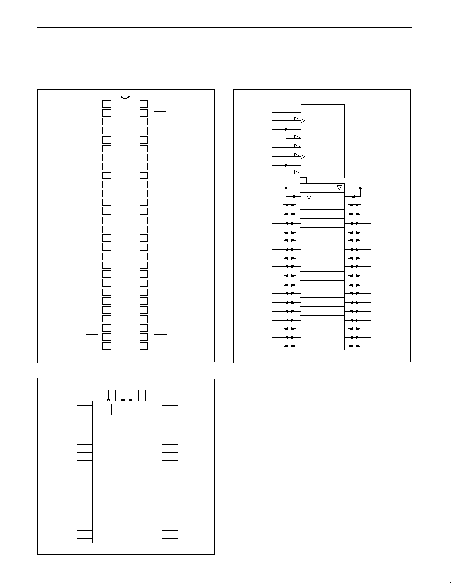
PIN DESCRIPTION
PIN NUMBER
SYMBOL
NAME AND FUNCTION
1
OEAB
A-to-B Output enable input
27
OEBA
B-to-A Output enable input (active low)
2, 28
LEAB/LEBA
A-to-B/B-to-A Latch enable input
55,30
CPAB/CPBA
A-to-B/B-to-A Clock input (active falling edge)
3, 5, 6, 8, 9, 10, 12, 13, 14, 15,
16, 17, 19, 20, 21, 23, 24, 26
A0-A17
Data inputs/outputs (A side)
54, 52, 51, 49, 48, 47, 45, 44, 43,
42, 41, 40, 38, 37, 36, 34, 33, 31
B0-B17
Data inputs/outputs (B side)
4, 11, 18, 25, 32, 39, 46, 53
GND
Ground (0V)
7, 22, 35, 50
V
CC
Positive supply voltage