1999 Sep 01
2
Philips Semiconductors
Product specification
32-bit bus transceiver with direction pin;
5 V tolerant; 3-state
74LVC32245A;
74LVCH32245A
FEATURES
·
5 V tolerant inputs/outputs for interfacing with 5 V logic
·
Wide supply voltage range of 1.2 to 3.6 V
·
Complies with JEDEC standard no. 8-1A
·
CMOS low power consumption
·
MULTIBYTE
TM
flow-trough standard pin-out architecture
·
Low inductance multiple power and ground pins for
minimum noise and ground bounce
·
Direct interface with TTL levels
·
Bus hold on data inputs (74LVCH32245A only)
·
Typical output ground bounce voltage:
V
OLP
< 0.8 V at V
CC
= 3.3 V; T
amb
= 25
°
C
·
Typical output V
OH
undershoot voltage:
V
OHV
> 2 V at V
CC
= 3.3 V; T
amb
= 25
°
C
·
Power-off disabled outputs, permitting live insertion
·
Plastic fine-pitch ball grid array package.
DESCRIPTION
The 74LVC(H)32245A is a high-performance, low-power,
low-voltage, Si-gate CMOS device, superior to most
advanced CMOS compatible TTL families. Inputs can be
driven from either 3.3 or 5 V devices. In 3-state operation,
outputs can handle 5 V. These features allow the use of
these devices in a mixed 3.3 and 5 V environment.
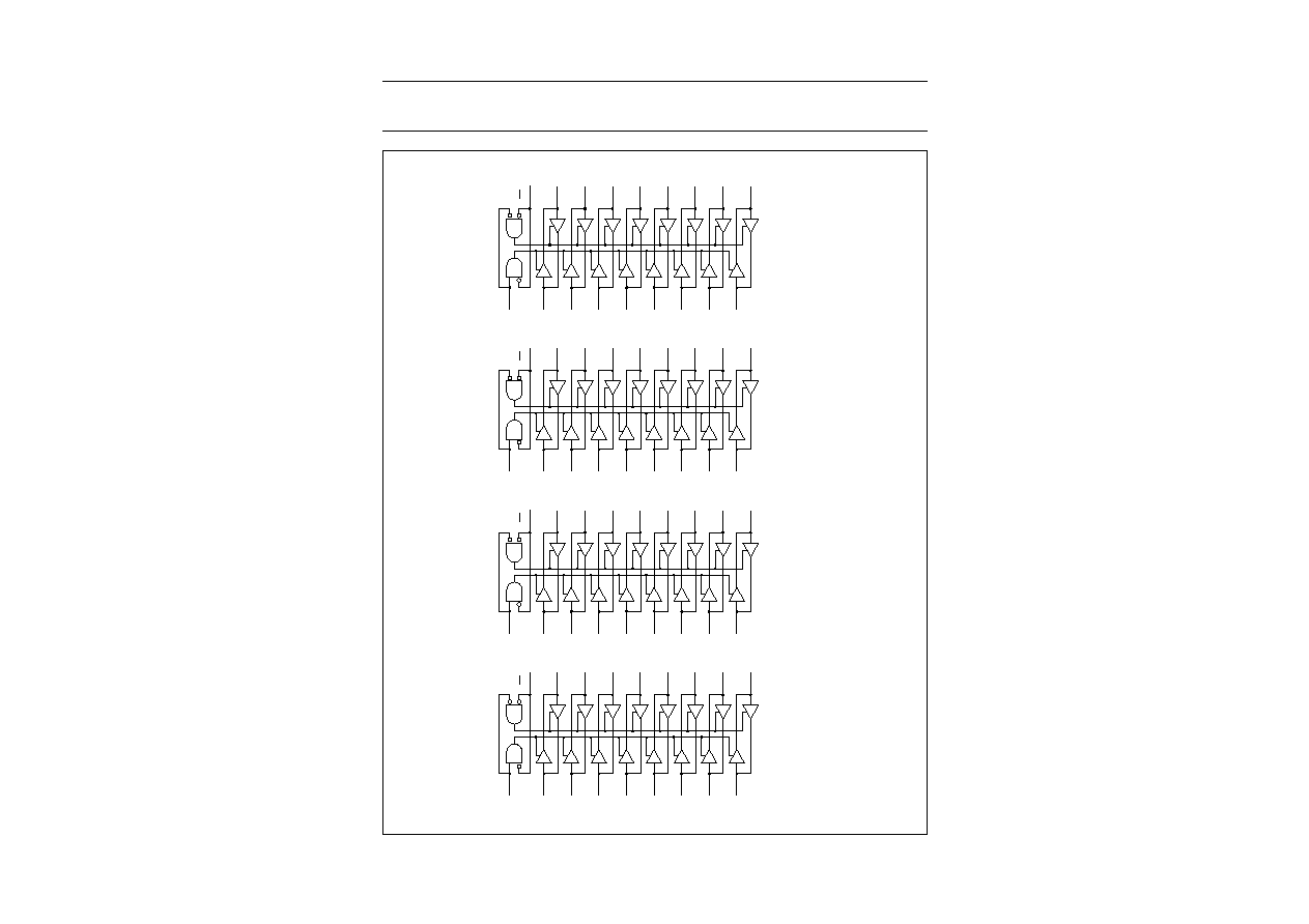
The 74LVC(H)32245A is a 32-bit transceiver featuring
non-inverting 3-state bus compatible outputs in both send
and receive directions. The 74LVC(H)32245A features two
output enable (nOE) inputs for easy cascading and two
send or receive (nDIR) inputs for direction control. nOE
controls the outputs so that the buses are effectively
isolated.
To ensure the high-impedance state during power-up or
power-down, input nOE should be tied to V
CC
through a
pull-up resistor; the minimum value of the resistor is
determined by the current-sinking capability of the driver.
The 74LVCH32245A bus hold data inputs eliminates the
need for external pull-up resistors to hold unused or
floating data inputs at a valid logic level (see Fig.2).
QUICK REFERENCE DATA
Ground = 0 V; T
amb
= 25
°
C; t
r
= t
f
2.5 ns.
Note
1. C
PD
is used to determine the dynamic power dissipation (P
D
in
µ
W).
P
D
= C
PD
×
V
CC
2
×
f
i
+
(C
L
×
V
CC
2
×
f
o
) where:
f
i
= input frequency in MHz;
f
o
= output frequency in MHz;
C
L
= output load capacitance in pF;
V
CC
= supply voltage in Volts;
(C
L
×
V
CC
2
×
f
o
) = sum of the outputs.
SYMBOL
PARAMETER
CONDITIONS
TYPICAL
UNIT
t
PHL
/t
PLH
propagation delay
nA
n
to nB
n
; nB
n
to nA
n
C
L
= 50 pF; V
CC
= 3.3 V
3.0
ns
C
I
input capacitance
5.0
pF
C
I/O
input/output capacitance
10
pF
C
PD
power dissipation capacitance per
buffer
V
I
= GND to V
CC
; note 1
30
pF
1999 Sep 01
3
Philips Semiconductors
Product specification
32-bit bus transceiver with direction pin;
5 V tolerant; 3-state
74LVC32245A;
74LVCH32245A
FUNCTION TABLE
See note 1.
Note
1. H = HIGH voltage level;
L = LOW voltage level;
X = don't care;
Z = high-impedance OFF-state.
ORDERING INFORMATION
PINNING
INPUT
OUTPUT
nOE
nDIR
nA
n
nB
n
L
L
A = B
inputs
L
H
inputs
B = A
H
X
Z
Z
TYPE NUMBER
PACKAGES
TEMPERATURE RANGE
PINS
PACKAGE
MATERIAL
CODE
74LVC32245AEC
-
40 to +85
°
C
96
LFBGA96
plastic
SOT536-1
74LVCH32245AEC
96
LFBGA96
plastic
SOT536-1
SYMBOL
DESCRIPTION
nDIR
direction control
nOE
output enable input (active LOW)
nA
n
data inputs/outputs
nB
n
data inputs/outputs
GND
ground (0 V)
V
CC
DC supply voltage
1999 Sep 01
4
Philips Semiconductors
Product specification
32-bit bus transceiver with direction pin;
5 V tolerant; 3-state
74LVC32245A;
74LVCH32245A
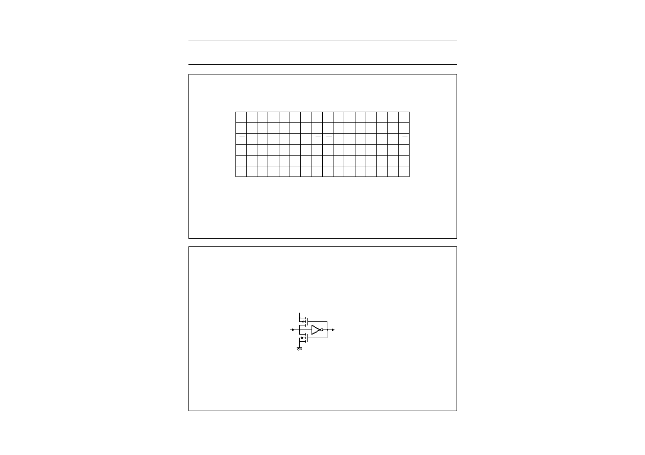
Fig.1 Pin configuration.
handbook, full pagewidth
MNA475
1A1 1A3 1A5 1A7 2A1 2A3 2A5 2A6 3A1 3A3 3A5 3A7 4A1 4A3 4A5 4A6
1A0 1A2 1A4 1A6 2A0 2A2 2A4 2A7 3A0 3A2 3A4 3A6 4A0 4A2 4A4 4A7
1B0 1B2 1B4 1B6 2B0 2B2 2B4 2B7 3B0 3B2 3B4 3B6 4B0 4B2 4B4 4B7
1B1 1B3 1B5 1B7 2B1 2B3 2B51 2B6 3B1 3B3 3B5 3B7 4B1 4B3 4B5 4B6
1OE
2OE 3OE
GND
GND GND
GND
4OE
VCC
VCC
GND
GND GND
GND
VCC
VCC
1DIR
6
5
2
1
4
3
2DIR 3DIR
GND
GND GND
GND
4DIR
VCC
VCC
GND
GND GND
GND
VCC
VCC
A
H
J
B
D
E
G
T
C
F
K
M
N
R
L
P
Fig.2 Bus hold circuit.
handbook, halfpage
MNA473
VCC
data
input
to internal circuit