2003 Feb 24
2
Philips Semiconductors
Product specification
Quad 2-input AND gate
74LVC08A
FEATURES
·
5 V tolerant inputs for interfacing with 5 V logic
·
Wide supply voltage range from 1.2 to 3.6 V
·
CMOS low power consumption
·
Direct interface with TTL levels
·
Inputs accept voltages up to 5.5 V
·
Complies with JEDEC standard no. 8-1A
·
ESD protection:
HBM EIA/JESD22-A114-A exceeds 2000 V
MM EIA/JESD22-A115-A exceeds 200 V.
·
Specified from
-
40 to +85
°
C and
-
40 to +125
°
C.
DESCRIPTION
The 74LVC08A is a high-performance, low-power,
low-voltage, Si-gate CMOS device, superior to most
advanced CMOS compatible TTL families.
Inputs can be driven from either 3.3 or 5 V devices. This
feature allows the use of these devices as translators in a
mixed 3.3 and 5 V environment.
The 74LVC08A provides the 2-input AND function.
QUICK REFERENCE DATA
GND = 0 V; T
amb
= 25
°
C; t
r
= t
f
2.5 ns.
Notes
1. C
PD
is used to determine the dynamic power dissipation (P
D
in
µ
W).
P
D
= C
PD
×
V
CC
2
×
f
i
×
N +
(C
L
×
V
CC
2
×
f
o
) where:
f
i
= input frequency in MHz;
f
o
= output frequency in MHz;
C
L
= output load capacitance in pF;
V
CC
= supply voltage in Volts;
N = total switching outputs;
(C
L
×
V
CC
2
×
f
o
) = sum of the outputs.
2. The condition is V
I
= GND to V
CC
.
ORDERING INFORMATION
SYMBOL
PARAMETER
CONDITIONS
TYPICAL
UNIT
t
PHL
/t
PLH
propagation delay nA, nB to nY
C
L
= 50 pF; V
CC
= 3.3 V
2.1
ns
C
I
input capacitance
4.0
pF
C
PD
power dissipation capacitance per gate
V
CC
= 3.3 V;
notes 1 and 2
10
pF
TYPE NUMBER
PACKAGE
TEMPERATURE RANGE
PINS
PACKAGE
MATERIAL
CODE
74LVC08AD
-
40 to +125
°
C
14
SO14
plastic
SOT108-1
74LVC08ADB
-
40 to +125
°
C
14
SSOP14
plastic
SOT337-1
74LVC08APW
-
40 to +125
°
C
14
TSSOP14
plastic
SOT402-1
74LVC08ABQ
-
40 to +125
°
C
14
DHVQFN14
plastic
SOT762-1
2003 Feb 24
4
Philips Semiconductors
Product specification
Quad 2-input AND gate
74LVC08A
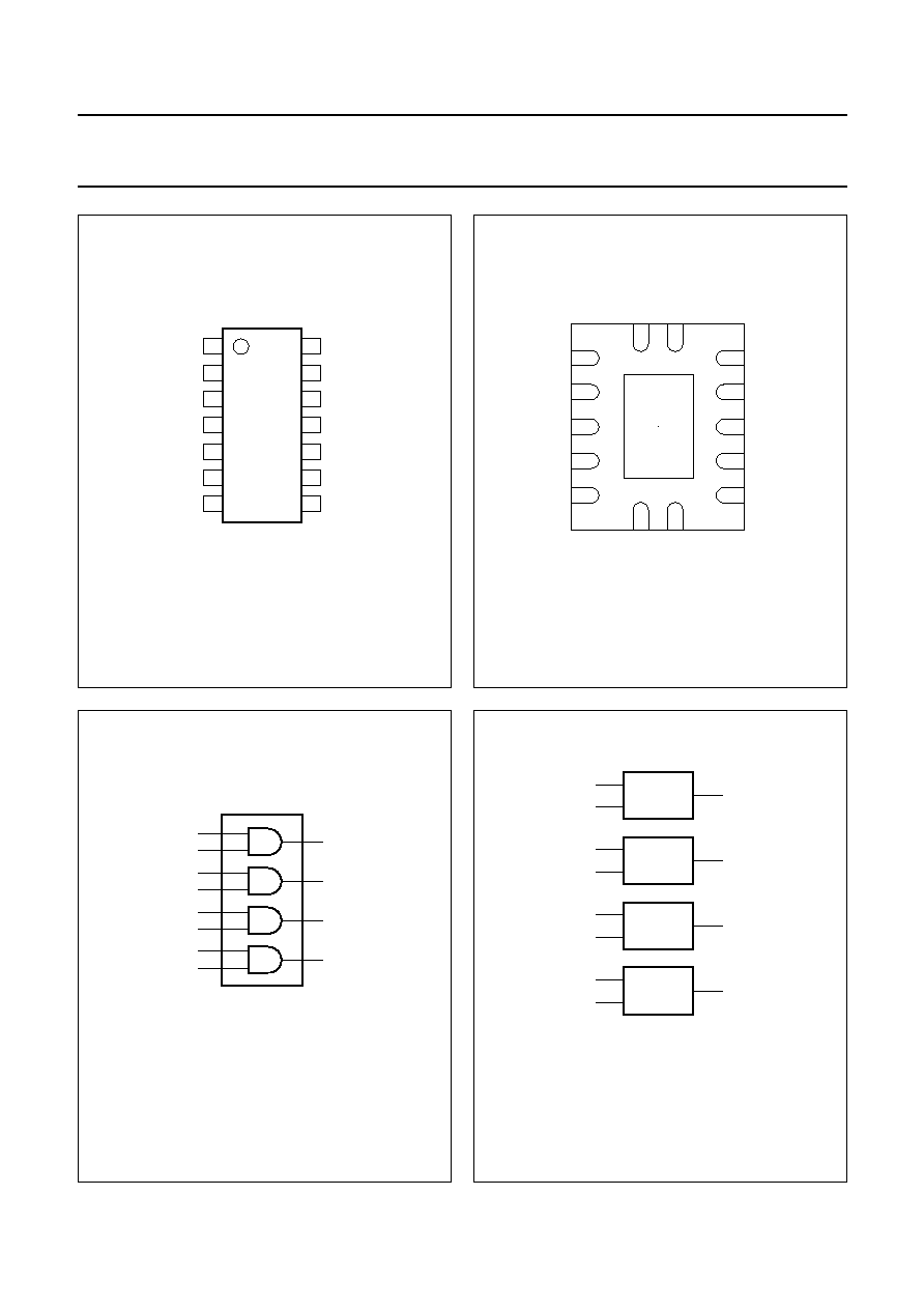
handbook, halfpage
MNA220
08
1
2
3
4
5
6
7
8
14
13
12
11
10
9
1A
1B
1Y
2A
2B
2Y
GND
3Y
3A
3B
4Y
4A
4B
VCC
Fig.1 Pin configuration SO14 and (T)SSOP14.
handbook, halfpage
1
14
GND
(1)
1A
VCC
7
2
3
4
5
6
1B
1Y
2A
2B
2Y
13
12
11
10
9
4B
4A
4Y
3B
3A
8
GND
Top view
3Y
MCE183
(1) The die substrate is attached to this pad using conductive die
attach material. It can not be used as a supply pin or input.
Fig.2 Pin configuration DHVQFN14.
handbook, halfpage
MNA222
1A
1B
1Y
2
1
3
2A
2B
2Y
5
4
6
3A
3B
3Y
10
9
8
4A
4B
4Y
13
12
11
Fig.3 Logic symbol.
handbook, halfpage
MNA223
3
&
&
&
&
2
1
6
5
4
8
10
9
11
13
12
Fig.4 Logic symbol (IEEE/IEC).