Document Outline
- FEATURES
- DESCRIPTION
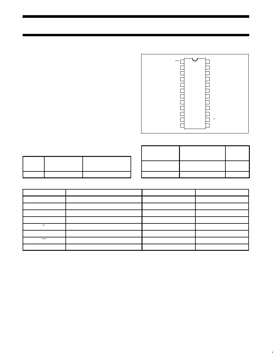
- PIN CONFIGURATION
- ORDERING INFORMATION
- INPUT AND OUTPUT LOADING AND FAN-OUT TABLE
- LOGIC SYMBOL
- IEC/IEEE SYMBOL
- TYPICAL TIMING DIAGRAM
- LOGIC DIAGRAM
- FUNCTION TABLE
- ABSOLUTE MAXIMUM RATINGS
- RECOMMENDED OPERATING CONDITIONS
- DC ELECTRICAL CHARACTERISTICS
- AC ELECTRICAL CHARACTERISTICS
- AC SETUP REQUIREMENTS
- AC WAVEFORMS
- TEST CIRCUIT AND WAVEFORMS
Philips Semiconductors
Product specification
74F835
8-bit shift register with 2:1 mux-in,
latched "B" inputs, and serial out
1
1990 Jan 08
8530615 99490
FEATURES
·
Specifically designed for Video applications
·
Combines the 74F373, two 74F157s, and the 74F166 functions in
one package
·
Interleaved loading with 2:1 mux
·
Dual 8-bit parallel inputs
·
Transparent latch on all "B" inputs
·
Guaranteed serial shift frequency to 100MHz
·
Expandable to 16-bits or more with serial input
DESCRIPTION
The 74F835 is a high speed 8-bit parallel/serial-in, serial-out shift
register whose parallel inputs have been connected to an internal
octal two-to-one multiplexer with all the "B" inputs connected to an
octal latch.
This 24-pin part is specifically designed for video bit shifting, where
interleaved loading is desired and parts count is critical. It is useful in
any design where a 2:1 mux input with a transparent latch is
needed.
TYPE
TYPICAL f
MAX
TYPICAL
SUPPLY CURRENT
(TOTAL)
74F835
150MHz
45mA
PIN CONFIGURATION
1
2
3
4
5
6
7
8
9
10
11
12
13
14
15
16
17
18
19
20
21
22
23
24
PE
CP
D4A
D4B
D5A
D5B
D6A
D6B
D7A
D7B
Q7
V
CC
D3B
D3A
D2B
D2A
D1B
D1A
D0A
D0B
DS
SA/B
LE
GND
SF01355
ORDERING INFORMATION
DESCRIPTION
COMMERCIAL RANGE
V
CC
= 5V
±
10%,
T
amb
= 0
°
C to +70
°
C
PACKAGE
DRAWING
NUMBER
24-pin plastic
Slim DIP (300 mil)
N74F835N
SOT222-1
24-pin plastic SOL
N74F835D
SOT137-1
INPUT AND OUTPUT LOADING AND FAN-OUT TABLE
PINS
DESCRIPTION
74F (U.L.) HIGH/LOW
LOAD VALUE HIGH/LOW
D0A D7A
Parallel data inputs
1.0/1.0
20
µ
A/0.6mA
D0B D7B
Latched Parallel data inputs
1.0/1.0
20
µ
A/0.6mA
DS
Serial data input
1.0/1.0
20
µ
A/0.6mA
CP
Shift Register Clock input (active rising edge)
1.0/1.0
20
µ
A/0.6mA
SA/B
Mux Select
1.0/1.0
20
µ
A/0.6mA
LE
Latch Enable input (for B inputs)
1.0/1.0
20
µ
A/0.6mA
PE
Parallel Enable input
1.0/1.0
20
µ
A/0.6mA
Q7
Output
50/33
1.0mA/20mA
NOTE: One (1.0) FAST unit load is defined as: 20
µ
A in the High state and 0.6mA in the Low state.
Philips Semiconductors
Product specification
74F835
8-bit shift register with 2:1 mux-in,
latched "B" inputs, and serial out
1990 Jan 08
2
LOGIC SYMBOL
2
1
13
14
CP
PE
LE
SA/B
15 16 17 18 19 20 21 22 23
3
4
5
6
7
8
9 10
11
Q7
DS
D0A
D0B
D1A
D1B
V
CC
= PIN 24
GND = PIN 12
SF01356
D2A
D2B
D3A
D3B
D4A
D4B
D5A
D5B
D6A
D6B
D7A
D7B
IEC/IEEE SYMBOL
SF01357
2
C1
SRG 8
MUX
1
M4
13
EN3
14
G2
15
1,4
16
1, 2, 3, 4
17
1, 2, 3, 4
18
19
20
21
22
23
3
4
5
6
7
8
9
10
11
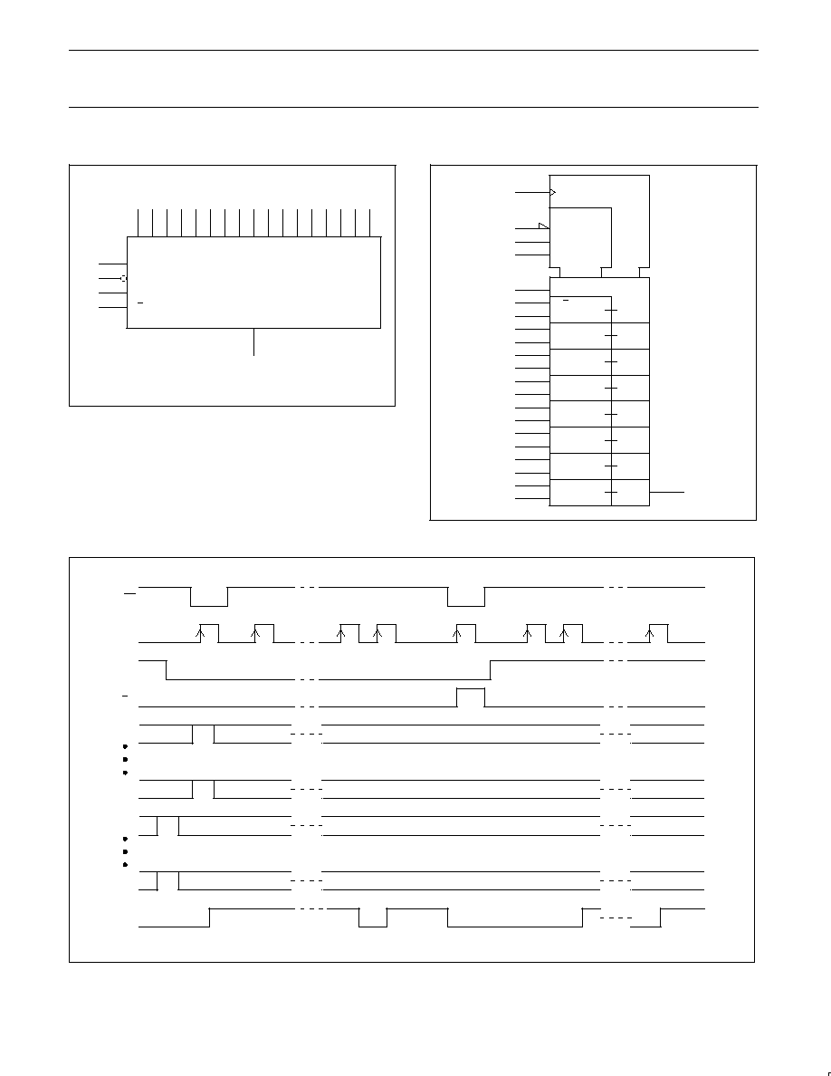
TYPICAL TIMING DIAGRAM
SET B
UNLOAD
B LATCH
SHIFT B
SHIFT A
LOAD A
LOAD B LATCH
PE
CP
LE
SA/B
ÉÉÉÉ
ÉÉÉÉ
ÉÉÉÉ
ÉÉÉÉ
ÉÉÉÉ
ÉÉÉÉ
ÉÉÉÉ
ÉÉÉÉ
ÉÉÉÉÉÉÉÉÉÉÉÉÉÉ
ÉÉÉÉÉÉÉÉÉÉÉÉÉÉ
ÉÉÉÉÉÉÉÉÉÉÉÉÉÉ
ÉÉÉÉÉÉÉÉÉÉÉÉÉÉ
ÉÉÉÉ
ÉÉÉÉ
ÉÉÉÉ
ÉÉÉÉ
ÉÉÉÉ
ÉÉÉÉ
ÉÉÉÉ
ÉÉÉÉ
ÉÉÉÉ
ÉÉÉÉ
ÉÉÉÉ
ÉÉÉÉ
ÉÉÉÉÉÉÉÉÉÉÉÉÉÉ
ÉÉÉÉÉÉÉÉÉÉÉÉÉÉ
ÉÉÉÉÉÉÉÉÉÉÉÉÉÉ
ÉÉÉÉÉÉÉÉÉÉÉÉÉÉ
ÉÉÉÉ
ÉÉÉÉ
ÉÉÉÉ
ÉÉÉÉ
ÉÉÉÉÉÉ
ÉÉÉÉÉÉ
ÉÉÉÉÉÉ
ÉÉÉÉÉÉ
ÉÉÉÉÉÉÉÉÉÉÉÉÉÉ
ÉÉÉÉÉÉÉÉÉÉÉÉÉÉ
ÉÉÉÉÉÉÉÉÉÉÉÉÉÉ
ÉÉÉÉÉÉÉÉÉÉÉÉÉÉ
ÉÉÉÉ
ÉÉÉÉ
ÉÉÉÉ
ÉÉÉÉ
ÉÉÉÉÉÉ
ÉÉÉÉÉÉ
ÉÉÉÉÉÉ
ÉÉÉÉÉÉ
ÉÉ
ÉÉ
ÉÉ
ÉÉ
ÉÉÉÉÉÉÉÉÉÉÉÉÉÉ
ÉÉÉÉÉÉÉÉÉÉÉÉÉÉ
ÉÉÉÉÉÉÉÉÉÉÉÉÉÉ
ÉÉÉÉÉÉÉÉÉÉÉÉÉÉ
ÉÉÉÉ
ÉÉÉÉ
ÉÉÉÉ
ÉÉÉÉ
D0A
D7A
D0B
D7B
ÉÉ
ÉÉ
ÉÉ
ÉÉ
Q7
q7A
q6A
q1A
q0A
q7B
q6B
q5B
q0B
SF01359

Philips Semiconductors
Product specification
74F835
8-bit shift register with 2:1 mux-in,
latched "B" inputs, and serial out
1990 Jan 08
3
LOGIC DIAGRAM
V
CC
= PIN 24
GND = PIN 12
D
Q
CP
D
Q
CP
D
Q
CP
D
Q
CP
D
Q
CP
D
Q
CP
D
Q
CP
D
Q
CP
11
Q7
D
E
Q
D
E
Q
D
E
Q
D
E
Q
D
E
Q
D
E
Q
D
E
Q
D
E
Q
16
17
18
19
20
21
22
23
3
4
5
6
7
8
9
10
D0A
D0B
D1A
D1B
D2A
D2B
D3A
D3B
D4A
D4B
D5A
D5B
D6A
D6B
D7A
D7B
LE
13
14
1
15
2
SA/B
PE
DS
CP
SF01358
FUNCTION TABLE
OPERATING
MODE
INPUTS
INTERNAL
OUTPUT
OPERATING
MODE
INPUTS
B
LATCH
SERIAL REGISTER
OUTPUT
MODE
PE
CP
LE
SA/B
DnA
DnB
DS
B
LATCH
Q0
Q16
Q7
Parallel load
A data
L
X
L
h
X
X
X
H
H
H
Parallel load
A data
L
X
L
l
X
X
X
L
L
L
Latch B data
X
X
L
X
X
h
X
H
X
X
X
Latch B data
X
X
L
X
X
l
X
L
X
X
X
Parallel load B data
(from Latch)
L
L
H
X
X
X
h
H
H
H
Parallel load B data
(from Latch)
L
L
H
X
X
X
l
L
L
L
Parallel load B data
(Transparent Mode)
L
H
H
X
h
X
h
H
H
H
Parallel load B data
(Transparent Mode)
L
H
H
X
l
X
l
L
L
L
Serial Shift
H
X
X
X
X
h
X
H
qn1
q6
Serial Shift
H
X
X
X
X
l
X
L
qn1
q6
H = High voltage level
L
= Low voltage level
h
= High voltage level one setup time prior to the Low-to-High clock transition
l
= Low voltage level one setup time prior to the Low-to-High clock transition
X = Don't care
qn = Lower case letters indicate the state of the referenced flop cell one cycle prior to the Low-to-High clock transition
= Low-to-High clock transition

Philips Semiconductors
Product specification
74F835
8-bit shift register with 2:1 mux-in,
latched "B" inputs, and serial out
1990 Jan 08
4
ABSOLUTE MAXIMUM RATINGS
(Operation beyond the limits set forth in this table may impair the useful life of the device.
Unless otherwise noted these limits are over the operating free-air temperature range.)
SYMBOL
PARAMETER
RATING
UNIT
V
CC
Supply voltage
0.5 to +7.0
V
V
IN
Input voltage
0.5 to +7.0
V
I
IN
Input current
30 to +5
mA
V
OUT
Voltage applied to output in High output state
0.5 to V
CC
V
I
OUT
Current applied to output in Low output state
40
mA
T
amb
Operating free-air temperature range
0 to +70
°
C
T
stg
Storage temperature range
65 to +150
°
C
RECOMMENDED OPERATING CONDITIONS
SYMBOL
PARAMETER
LIMITS
UNIT
SYMBOL
PARAMETER
MIN
NOM
MAX
UNIT
V
CC
Supply voltage
4.5
5.0
5.5
V
V
IH
High-level input voltage
2.0
V
V
IL
Low-level input voltage
0.8
V
I
IK
Input clamp current
18
mA
I
OH
High-level output current
1
mA
I
OL
Low-level output current
20
mA
T
amb
Operating free-air temperature range
0
+70
°
C
DC ELECTRICAL CHARACTERISTICS
(Over recommended operating free-air temperature range unless otherwise noted.)
SYMBOL
PARAMETER
TEST CONDITIONS
1
LIMITS
UNIT
SYMBOL
PARAMETER
TEST CONDITIONS
1
MIN
TYP
2
MAX
UNIT
V
OH
High-level output voltage
V
CC
= MIN, V
IL
= MAX
V
IH
= MIN, I
OH
= MAX
±
10% V
CC
2.5
V
V
OH
High-level output voltage
V
CC
= MIN, V
IL
= MAX
V
IH
= MIN, I
OH
= MAX
±
5% V
CC
2.7
3.4
V
V
OL
Low-level output voltage
V
CC
= MIN, V
IL
= MAX
V
IH
= MIN, I
OH
L= MAX
±
10% V
CC
0.30
0.50
V
V
OL
Low-level output voltage
V
CC
= MIN, V
IL
= MAX
V
IH
= MIN, I
OH
L= MAX
±
5% V
CC
0.30
0.50
V
V
IK
Input clamp voltage
V
CC
= MIN, I
I
= I
IK
0.73
1.2
V
I
I
Input current at maximum input voltage
V
CC
= MAX, V
I
= 7.0V
100
µ
A
I
IH
High-level input current
V
CC
= MAX, V
I
= 2.7V
20
µ
A
I
IL
Low-level input current
V
CC
= MAX, V
I
= 0.5V
0.6
mA
I
OS
Short circuit output current
3
V
CC
= MAX
60
150
mA
I
CC
Supply current (total)
V
CC
= MAX
45
65
mA
NOTES:
1. For conditions shown as MIN or MAX, use the appropriate value specified under recommended operating conditions for the applicable type.
2. All typical values are at V
CC
= 5V. T
amb
= 25
°
C.
3. Not more than one output should be shorted at a time. For testing I
OS
, the use of high-speed test apparatus and/or sample-and-hold
techniques are preferable in order to minimize internal heating and more accurately reflect operational values. Otherwise, prolonged shorting
of a High output may raise the chip temperature well above normal and thereby cause invalid readings in other tests. In any sequence of
parameter tests, I
OS
tests should be performed last.

Philips Semiconductors
Product specification
74F835
8-bit shift register with 2:1 mux-in,
latched "B" inputs, and serial out
1990 Jan 08
5
AC ELECTRICAL CHARACTERISTICS
SYMBOL
PARAMETER
TEST
CONDITION
LIMITS
UNIT
SYMBOL
PARAMETER
TEST
CONDITION
T
amb
= +25
°
C
V
CC
= +5.0V
C
L
= 50pF, R
L
= 500
T
amb
= 0
°
C to +70
°
C
V
CC
= +5.0V
±
10%
C
L
= 50pF, R
L
= 500
UNIT
MIN
TYP
MAX
MIN
MAX
f
MAX
Maximum clock frequency
Waveform 1
130
150
100
MHz
t
PLH
t
PHL
Propagation delay
CP to Q7 (Load)
Waveform 1
5.0
5.0
7.0
7.0
9.5
9.5
5.0
5.0
10.0
10.0
ns
t
PLH
t
PHL
Propagation delay
CP to Q7 (Shift)
Waveform 1
5.0
5.0
7.0
7.0
9.5
9.5
5.0
5.0
10.0
10.0
ns
AC SETUP REQUIREMENTS
SYMBOL
PARAMETER
TEST
CONDITION
LIMITS
UNIT
SYMBOL
PARAMETER
TEST
CONDITION
T
amb
= +25
°
C
V
CC
= +5.0V
C
L
= 50pF, R
L
= 500
T
amb
= 0
°
C to +70
°
C
V
CC
= +5.0V
±
10%
C
L
= 50pF, R
L
= 500
UNIT
MIN
TYP
MAX
MIN
MAX
t
s
(H)
t
s
(L)
Setup time
DnA or DnB to CP
Waveform 2
3.5
3.5
3.5
3.5
ns
t
h
(H)
t
h
(L)
Hold time
DnA or DnB to CP
Waveform 2
1.0
1.0
1.5
1.5
ns
t
s
(H)
t
s
(L)
Setup time
DS to CP
Waveform 2
1.0
1.0
1.5
1.5
ns
t
h
(H)
t
h
(L)
Hold time
DS to CP
Waveform 2
2.0
2.0
2.5
2.5
ns
t
s
(H)
t
s
(L)
Setup time
PE to CP
Waveform 2
3.5
3.5
4.0
4.0
ns
t
h
(H)
t
h
(L)
Hold time
PE to CP
Waveform 2
0.0
0.0
0.0
0.0
ns
t
s
(H)
t
s
(L)
Setup time
DnB to LE
Waveform 2
0.0
0.0
0.0
0.0
ns
t
h
(H)
t
h
(L)
Hold time
DnB to LE
Waveform 2
3.0
3.0
4.0
4.0
ns
t
s
(H)
t
s
(L)
Setup time
SA/B to CP
Waveform 2
4.5
4.5
5.0
5.0
ns
t
h
(H)
t
h
(L)
Hold time
SA/B to CP
Waveform 2
0.0
0.0
0.0
0.0
ns
t
w
(H)
t
w
(L)
clock pulse width,
High or Low
Waveform 1
4.5
4.5
5.5
5.0
ns
t
w
(H)
Latch Enable pulse width,
High
Waveform 1
4.5
5.0
ns