1999 Nov 23
2
Philips Semiconductors
Product specification
16-bit transceiver/register with dual enable; 3-state
74ALVCH16652
FEATURES
·
In accordance with JEDEC standard no. 8-1A
·
CMOS low power consumption
·
MULTIBYTE
TM
flow-through pin-out architecture
·
Low inductance, multiple supply and ground pins for
minimum noise and ground bounce
·
Direct interface with TTL levels
·
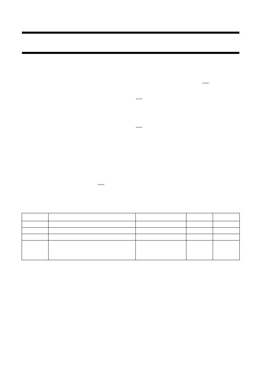
All data inputs have bus hold
·
Output drive capability 50
transmission lines at 85
°
C
·
Current drive
±
24 mA at 3.0 V.
DESCRIPTION
The 74ALVCH16652 consists of 16 non-inverting bus
transceiver circuits with 3-state outputs, D-type flip-flops
and control circuitry arranged for multiplexed transmission
of data directly from the data bus or from the internal
storage registers.
Data on the `A' or `B', or both buses, will be stored in the
internal registers, at the appropriate clock inputs
(nCP
AB
or nCP
BA
) regardless of the select inputs (nS
AB
and nS
BA
) or output enable (nOE
AB
and nOE
BA
) control
inputs.
Depending on the select inputs nS
AB
and nS
BA
data can
directly go from input to output (real-time mode) or data
can be controlled by the clock (storage mode), when OE
inputs permit this operating mode.
The output enable inputs nOE
AB
and nOE
BA
determine the
operation mode of the transceiver. When nOE
AB
is LOW,
no data transmission from nB
n
to nA
n
is possible and when
nOE
BA
is HIGH, no data transmission from nB
n
to nA
n
is
possible.
When nS
AB
and nS
BA
are in the real-time transfer mode, it
is also possible to store data without using the internal
D-type flip-flops by simultaneously enabling nOE
AB
and
nOE
BA
. In this configuration each output reinforces its
input.
Active bus hold circuitry is provided to hold unused or
floating data inputs at a valid logic level.
QUICK REFERENCE DATA
Ground = 0; T
amb
= 25
°
C; t
r
= t
f
= 2.5 ns.
Notes
1. C
PD
is used to determine the dynamic power dissipation (P
D
in
µ
W).
P
D
= C
PD
×
V
CC
2
×
f
i
+
(C
L
×
V
CC
2
×
f
o
) where:
f
i
= input frequency in MHz;
C
L
= output load capacitance in pF;
f
o
= output frequency in MHz;
V
CC
= supply voltage in Volts;
(C
L
×
V
CC
2
×
f
o
) = sum of outputs.
2. The condition is V
I
= GND to V
CC
.
SYMBOL
PARAMETER
CONDITIONS
TYPICAL
UNIT
t
PHL
/t
PLH
propagation delay nA
n
, nB
n
to nB
n
, nA
n
C
L
= 50 pF; V
CC
= 3.3 V
2.6
ns
f
max
maximum clock frequency
350
MHz
C
I
input capacitance
4.0
pF
C
PD
power dissipation capacitance per latch
notes 1 and 2
outputs enabled
22
pF
outputs disabled
4.0
pF
1999 Nov 23
3
Philips Semiconductors
Product specification
16-bit transceiver/register with dual enable; 3-state
74ALVCH16652
FUNCTION TABLE
See note 1.
Notes
1. H = HIGH voltage level;
L = LOW voltage level;
X = don't care;
= LOW-to-HIGH.
2. The data output functions may be enabled or disabled by various signals at the nOE
AB
and nOE
BA
inputs. Data input
functions are always enabled, i.e., data at the bus inputs will be stored on every LOW-to-HIGH transition on the clock
inputs.
INPUTS
DATA I/O
FUNCTION
nOE
AB
nOE
BA
nCP
AB
nCP
BA
nS
AB
nS
BA
nA
0
to nA
7
nB
0
to nB
7
L
L
H
H
H or L
H or L
X
X
X
X
input
input
isolation store A and B data
X
H
H
H
H or L
X
L
X
X
input
input
unspecified
(2)
output
store A, hold B
store A in both registers
L
L
X
L
H or L
X
X
X
L
unspecified
(2)
output
input
input
hold A, store B
store B in both registers
L
L
L
L
X
X
X
H or L
X
X
L
H
output
input
real-time B data to A bus
stored B data to A bus
H
H
H
H
X
H or L
X
X
L
H
X
X
input
output
real-time A data to B bus
stored A data to B bus
H
L
H or L
H or L
H
H
output
output
stored A data to B bus and
stored B data to A bus
1999 Nov 23
4
Philips Semiconductors
Product specification
16-bit transceiver/register with dual enable; 3-state
74ALVCH16652
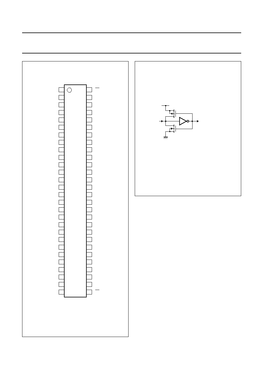
ORDERING INFORMATION
PINNING
OUTSIDE NORTH
AMERICA
NORTH
AMERICA
PACKAGE
TEMPERATURE
RANGE
PINS
PACKAGE
MATERIAL
CODE
74ALVCH16652DGG
ACH16652 DGG
-
40 to +85
°
C
56
TSSOP
plastic
SOT364-1
PIN
SYMBOL
DESCRIPTION
1 and 28
1OE
AB
, 2OE
AB
output enable A-to-B
2 and 27
1CP
AB
, 2CP
AB
clock input A-to-B
3 and 26
1S
AB
, 2S
AB
select input A-to-B
5, 6, 8, 9, 10, 12, 13 and 14
1A
0
to 1A
7
`1A' data inputs/outputs
4, 11, 18, 25, 32, 39, 46 and 53
GND
ground (0 V)
7, 22, 35, 50
V
CC
positive supply voltage
15, 16, 17, 19, 20, 21, 23 and 24
2A
0
to 2A
7
`2A' data inputs/outputs
29 and 56
2OE
BA
, 1OE
BA
output enable B-to-A
30 and 55
2CP
BA
, 1CP
BA
clock input B-to-A
31 and 54
2S
BA
, 1S
BA
select input B-to-A
33, 34, 36, 37, 38, 40, 41 and 42
2B
0
to 2B
7
`2B' data inputs/outputs
43, 44, 45, 47, 48, 49, 51 and 52
1B
7
to 1B
0
`1B' data inputs/outputs